

Page 1

INTEGRATED CIRCUITS
DATA SH EET
PCF84CxxxA family
8-bit microcontrollers
Product specification
Supersedes data of May 1994
File under Integrated Circuits, IC14
1996 Nov 22
Page 2

Philips Semiconductors Product specification
8-bit microcontrollers PCF84CxxxA family
CONTENTS
1 INTRODUCTION
2 FEATURES
3 GENERAL DESCRIPTION
4 BLOCK DIAGRAM
5 PINNING INFORMATION
5.1 Pinning
5.2 Pin description
6 FUNCTIONAL DESCRIPTION
6.1 Central processing unit
6.2 Program memory
6.3 Data memory
6.3.1 Working registers
6.3.2 Program Counter stack
6.4 Program Counter
6.5 Program Status Word
6.6 Interrupts
6.6.1 External interrupt
6.6.2 I2C-bus/Derivative interrupt
6.6.3 Timer/event counter interrupt
6.7 Timer/event counter 1
6.7.1 Test 1/count input (T1)
6.8 Parallel ports
6.9 I2C-bus interface
6.9.1 Data shift register (S0)
6.9.2 Address register (S0’)
6.9.3 Clock control register (S2)
6.9.4 Status Register (S1)
6.10 Timing
6.11 Oscillator
6.12 Reset
6.12.1 Passive external reset
6.12.2 Active external reset
6.12.3 Internal reset
6.12.4 Reset state
6.13 Reduced power modes
6.13.2 Stop mode
6.14 Derivative logic
7 INSTRUCTION SET
7.1 Instruction map
8 DEFINITIONS
9 LIFE SUPPORT APPLICATIONS
10 PURCHASE OF PHILIPS I2C COMPONENTS
1996 Nov 22 2
Page 3

Philips Semiconductors Product specification
8-bit microcontrollers PCF84CxxxA family
1 INTRODUCTION
This data sheet describes the shared properties of the
PCF84CxxxA family of microcontrollers. The family
currently consists of:
• PCF84C00
• PCF84C12A; 22A; 42A
• PCF84C21A; 41A; 81A
• PCF84C85A
• PCF84C122; 222; 422; 622; 822
• PCF84C44x; 64x; 84x
• PCF84C846.
For a particular microcontroller, this data sheet should be
read in conjunction with the individual data sheet of the
specific device. Data sheets can be found in
Handbook IC14, “8048-based 8-bit microcontrollers”
The PCD33xxA family of microcontrollers has similar
characteristics to the PCF84CxxxA family, but with lower
minimum operating voltage, DTMF/modem/musical tone
generation and (for most devices) on-chip EEPROM. This
family should be considered for telecom-specific
applications. Please refer to the
sheet.
“PCD33xxA family”
“Data
.
data
3 GENERAL DESCRIPTION
The PCF84CxxxA family of microcontrollers provide up to
8 kbytes of program memory and up to 256 bytes of RAM.
All devices include flexible I/O ports, an 8-bit
programmable timer/event counter and a choice of
single-level vectored interrupts. Most devices feature
2
C-bus compatibility. The instruction set is based on that
I
of the well-known MAB8048. Some of the devices have
functional equivalents in the MAB84xx family of NMOS
controllers. Where the lower power consumption and
higher speed of CMOS provide advantages, the
PCF84CxxxA devices can be used as direct replacements
for their MAB84xx equivalents.
A range of prototyping devices with external program
memory and ‘Piggy-backs’, as well as emulation probes
and prototyping systems are available.
2 FEATURES
• 8-bit CPU, ROM, RAM, I/O all in one package
• Up to 8 kbytes ROM
• Up to 256 bytes RAM
• Over 100 instructions (based on MAB8048) all of
1 or 2 cycles
• 8 or more quasi-bidirectional I/O port lines
• 8-bit programmable timer/event counter 1
• 2 or 3 single-level vectored interrupts: external,
timer/event counter, (I
• Two test inputs, one of which also serves as the external
interrupt input
• I2C-bus serial data interface (most devices)
• Derivative logic (most devices)
• Power-on-reset, Stop and Idle modes
• Supply voltage range: 2.5 to 6 V
• Clock frequency: 1 to 16 MHz
• Operating temperature: −40 to +85 °C
• Manufactured in silicon gate CMOS process.
2
C-bus/derivative)
1996 Nov 22 3
Page 4
Philips Semiconductors Product specification
8-bit microcontrollers PCF84CxxxA family
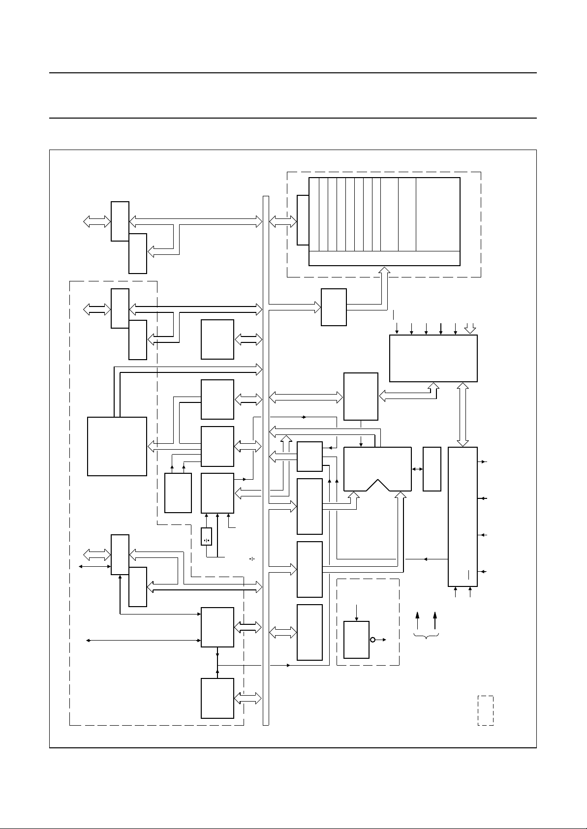
4 BLOCK DIAGRAM
MBA283 - 2
P0.7 to P0.0
P1.7 to P1.0
P2.2 to P2.0
3
SDA/P2.3
SCLK
PORT 0
BUFFER
PORT 0
PORT 1
BUFFER
PORT 1
UP TO
8 kbytes
DECODE
RESIDENT ROM
PORT 2
BUFFER
PORT 2
DATACLOCK
FLIP-FLOPS
FLIP-FLOPS
FLIP-FLOPS
13
BANK
MEMORY
FLIP-FLOPS
WORD
STATUS
PROGRAM
LOWER
COUNTER
PROGRAM
HIGHER
COUNTER
PROGRAM
EVENT
TIMER/
COUNTER
32
C-BUS
2
I
INTERFACE
(8)
(5)
Timer
interrupt
(8)
T1
FREQ.
CLOCK
INTERNAL
8
30
848 858878 8
REGISTER 0
REGISTER 1
REGISTER 2
MULTIPLEXER
RAM
ADDRESS
RUPT
LOGIC
INTER -
(8)
REGISTER 2
TEMPORARY
(8)
REGISTER 1
TEMPORARY
(8)
ACCUMULATOR
REGISTER 3
REGISTER 4
REGISTER 5
REGISTER 6
DECOD
REGISTER
&
REGISTER
INSTRUCTION
LOGIC UNIT
ARITHMETIC
POR
V
ON
RESET
POWER
REGISTER 7
8-LEVEL STACK
OPTIONAL SECOND
(VARIABLE LENGTH)
E
INT / T0
DECODER
RESET
DATA STORE
REGISTER BANK
FLAG
CARRY
T1
TIMER
LOGIC
BRANCH
CONDITIONAL
(8)
ADJUST
DECIMAL
external
interrupt
GND
SS
VDDV
POWER
SUPPLY
UP TO 256 bytes
RESIDENT RAM ARRAY
TEST
ACC
ACC BIT
XTAL 2XTAL 1RESETINT / T0
XTAL
OSCILLATOR
CONTROL & TIMING
STOP
INITIALIZE
INTERRUPT
IDLE
handbook, full pagewidth
Fig.1 Block diagram.
LOGIC
DERIVATIVE
SIO / derivative
1996 Nov 22 4
= type dependent
interrupt
Page 5

Philips Semiconductors Product specification
8-bit microcontrollers PCF84CxxxA family
5 PINNING INFORMATION
5.1 Pinning
For individual pinning configurations consult the data
5.2 Pin description
Table 1 describes the common functions of the devices.
For full details of pin descriptions consult the data sheet of
the specific device.
sheet of the specific device.
Table 1 Common functions
SYMBOL TYPE DESCRIPTION
V
SS
V
DD
P ground
P positive supply voltage
XTAL1 I crystal oscillator/external clock input
XTAL2 O crystal oscillator output
RESET I Reset input
INT/T0 I Interrupt/Test 0 input
T1 I Test 1/count input of 8-bit timer/event counter 1
P0.0 to P0.7 I/O Port 0: quasi-bidirectional I/O lines
P1.0 to P1.7 I/O Port 1: quasi-bidirectional I/O lines
P2.0 to P2.2 I/O Port 2: quasi-bidirectional I/O lines
2
SDA/P2.3 I/O bidirectional data line of the I
SCLK I/O bidirectional clock line of the I
C-bus interface/Port 2: quasi-bidirectional I/O line
2
C-bus interface
1996 Nov 22 5
Page 6

Philips Semiconductors Product specification
8-bit microcontrollers PCF84CxxxA family
6 FUNCTIONAL DESCRIPTION
6.1 Central processing unit
The PCF84CxxxA family provides an instruction set with
arithmetic, logic, branching, input/output and control
facilities. Special highlights are the instructions for BCD
arithmetic, nibble handling, conditional branches, loop
control (DJNZ) and table look-up (MOVP).
Code and execution efficiency is achieved by using a
maximum of two bytes and two execution cycles per
instruction (see Chapter 7).
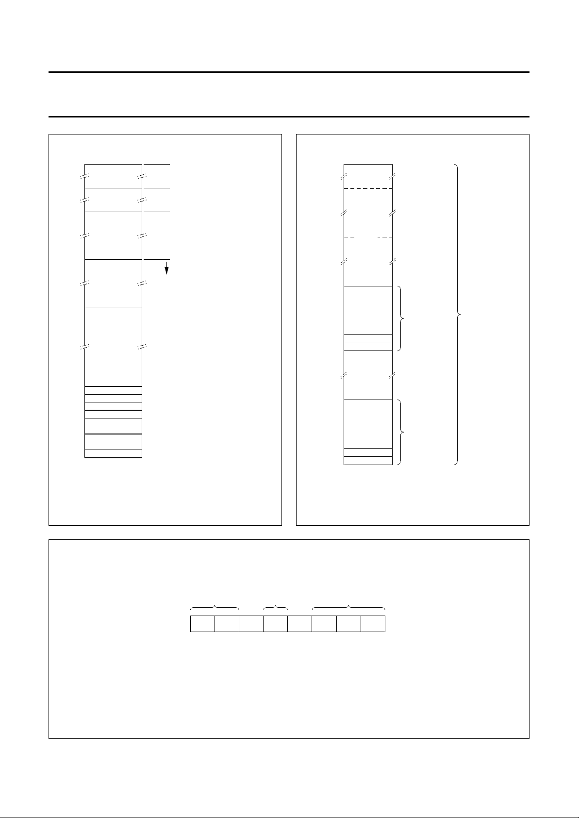
6.2 Program memory
The program memory consists of up to 8 kbytes of
read-only memory (ROM). Each location is directly
addressable by the Program Counter. The program
memory is mask-programmed at the factory. Figure 2
illustrates the program memory map.
Four program memory locations are of special importance:
• Location 0: first instruction to be executed after the
processor is reset
• Location 3: first instruction of an external interrupt
INT/T0) routine
(
• Location 5: first instruction of a I2C-bus/derivative
interrupt routine
• Location 7: first instruction of a timer/event counter
interrupt routine.
Only 11 bits of the 13-bit Program Counter function as a
counter. The two most significant bits can only be preset.
The program memory is therefore, structured into banks of
2 kbytes. Transfer of control to other memory banks is
performed by unconditional branches (JMP) or subroutine
calls (CALL) when another memory bank has been
pre-selected (by SEL MB instruction).
Each program memory bank is further divided into 8 pages
of 256 bytes. Indirect (JMPP) and conditional branches
cannot cross page boundaries.
6.3 Data memory
Data memory consists of up to 256 bytes of random
access memory (RAM). All locations are indirectly
addressable using RAM pointer registers. Up to
16 register locations are directly addressable. Data
memory also includes an 8-level Program Counter stack
addressed by a 3-bit Stack Pointer. All RAM locations
make efficient program loop counters if used with the
decrement register and test instruction (DJNZ). Figure 3
illustrates the data memory map.
6.3.1 W
Locations 0 to 7 are working registers. They are
accessible by efficient one byte/one cycle instructions,
thus making these locations suitable for frequently
accessed intermediate results.
As an alternative to locations 0 to 7, locations 24 to 31
may be used as working registers. Register bank selection
is made by SEL RB0/RB1 instructions. Register bank 1
may be used as an extension of register bank 0, as an
alternative register bank for interrupt service or as general
purpose data memory.
The first two locations of each bank (R0, R1, R0’ and R1’)
serve as RAM pointers that indirectly address all RAM
locations.
6.3.2 P
Locations 8 to 23 may be used as an 8-level Program
Counter stack reserving 2 locations per level, or as
general purpose RAM. The stack (see Fig.5) saves return
addresses and status during interrupt or subroutine
servicing. Nesting of subroutines and/or interrupts is
permitted up to 8-levels deep.
The 3-bit Stack Pointer always points to the next free stack
level. Following device reset, the Stack Pointer points to
level 0 (locations 8 and 9). On each subroutine call (CALL)
or interrupt, the contents of the Program Counter and
bits 4, 6 and 7 of the Program Status Word are transferred
to the level indicated by the Stack Pointer. The Stack
Pointer increments and points to the next free level.
Overflow from level 7 to level 0 occurs after nesting eight
levels deep. Further subroutine calls and/or interrupts
must not occur at this stage since this would result in loss
of program content; overriding level 0 content.
Return from interrupt must be performed by the RETR
instruction, which decrements the Stack Pointer and
restores the Program Counter and Program Status Word,
valid before the interrupt occurred. Return from subroutine
should be performed by the RET instruction. In contrast to
RETR, RET does not restore the Program Status Word.
As a general rule, the use of RETR in conjunction with a
subroutine call is not recommended. The use of RETR
must also be avoided with subroutines called from
interrupt routines because it prematurely terminates the
interrupt state (see Section 6.6).
ORKING REGISTERS
ROGRAM COUNTER STACK
1996 Nov 22 6
Page 7
Philips Semiconductors Product specification
8-bit microcontrollers PCF84CxxxA family
8191
handbook, halfpage
6143
4095
2048
2047
1024
1023
8
7
6
5
4
3
2
1
0
SEL MB3
SEL MB2
SEL MB1
SEL MB0
location 7: timer/event counter interrupt
vector
location 5: SIO/derivative interrupt
vector
location 3: external interrupt vector
location 0: reset vector
MBA284
255
128
127
64
63
32
31
25
24
23
8
7
1
0
USER
RAM
BANK 1
WORKING
REGISTERS
8 x 8
R1'
R0'
8-LEVEL
STACK
or
USER RAM
16 x 8
BANK 0
WORKING
REGISTERS
8 x 8
R1
R0
MLA616
directly
addressable
when Bank 1
is selected
directly
addressable
when Bank 0
is selected
addressed
indirectly
through pointers
R0, R1, R0', R1'
Fig.2 Program memory map. Fig.3 Data memory map.
saved in
handbook, halfpage
the stack
ACCY
76543
MSB LSB
1
saved in
the stack
RBS PS
Fig.4 Program Status Word.
1996 Nov 22 7
stack pointer
SP
SP1SP
2
21
0
0
MLA617
Page 8
Philips Semiconductors Product specification
8-bit microcontrollers PCF84CxxxA family
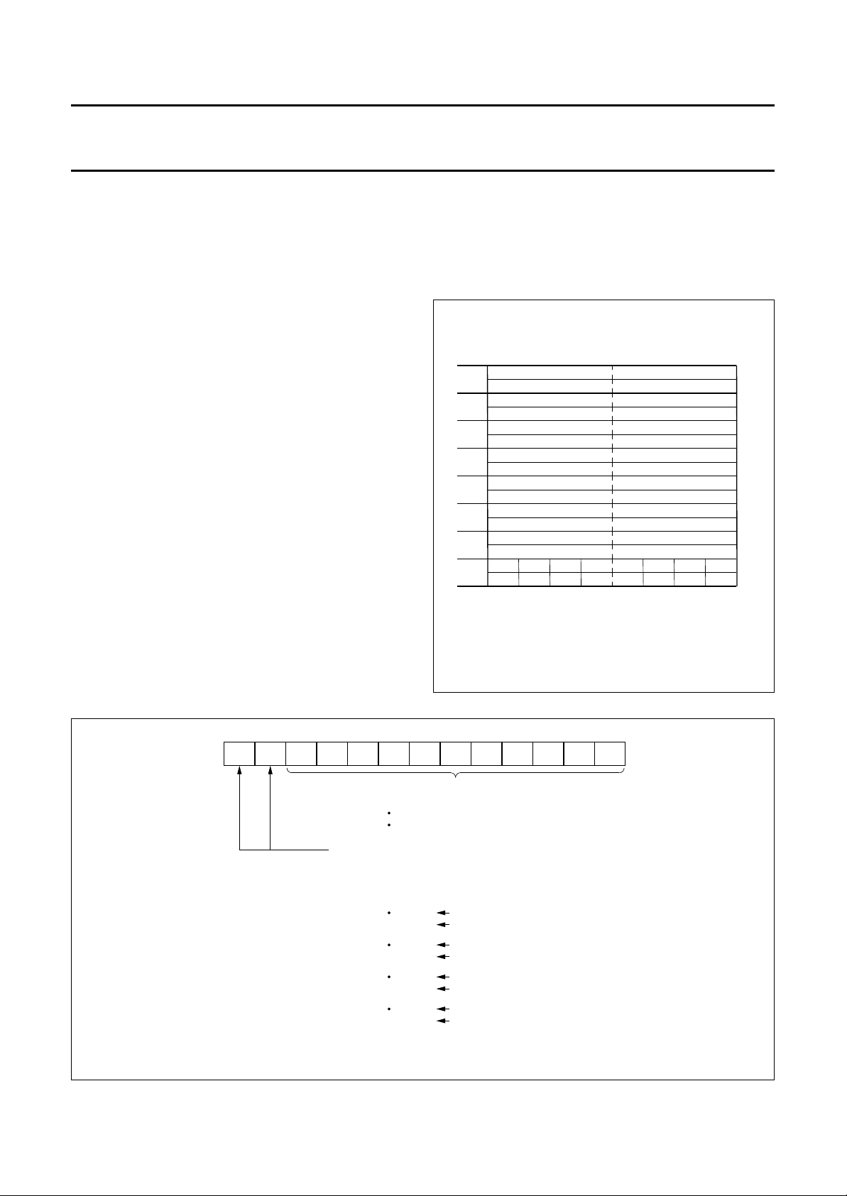
6.4 Program Counter
The 13-bit Program Counter is able to address up to
8 kbytes of ROM (see Fig.6). 11 bits (PC0 to PC10) are
auto-incrementing. The two most significant bits
(PC11 and PC12) must be changed under program
control by SEL MB followed by a JMP or CALL instruction.
6.5 Program Status Word
The Program Status Word (PSW) is an 8-bit register in the
CPU which stores information about the current status of
the microcontroller (see Fig.4).
The PSW bits are:
• Bits 0 to 2: Stack Pointer bits (SP0, SP1, SP2)
• Bit 3: timer Prescaler Select (PS); 0 = modulo-32,
1 = modulo-1 (no prescaling)
• Bit 4: working Register Bank Select (RBS);
0 = register bank 0, 1 = register bank 1
• Bit 5: not used (fixed at 1)
• Bit 6: Auxiliary Carry (AC); half-carry bit generated by an
ADD instruction and used by the decimal adjust
instruction DA A
• Bit 7: Carry (CY); the carry flag indicates that the
previous operation resulted in an overflow of the
Accumulator.
interrupts. Bit 3 can be controlled by MOV PSW, A and
bit 4 by SEL RB instructions. Bit 6 is set and cleared as a
side-effect of ADD and ADDC instructions. Bit 7 is affected
by ADD, ADDC, DA, RLC, RRC, CLR C and CPL C
instructions.
PC
10
DATA MEMORY
LOCATION
PC
PC
PC
8
9
LSB
MEA030
23
22
21
20
19
18
17
16
15
14
13
12
11
10
9
8
STACK
POINTER
handbook, halfpage
111
110
101
100
011
010
001
000
PSW
MSB
7PC6PC5PC4PC3PC2PC1PC0
PCPSW
7
12
6
PSW
PC
11
4
All bits can be read using the MOV A, PSW instruction.
Bits 0, 1 and 2 are affected by CALL, RET, RETR and
handbook, full pagewidth
PC12PC11PC10PC9PC8PC7PC6PC5PC4PC3PC2PC1PC
JMP or CALL instructions transfer the
contents of internal flipflop MBFF0 to PC
and MBBF1 to PC
Fig.6 Program Counter.
Fig.5 Program Counter Stack.
Conventional Program Counter
counts 000H to 7FFH
overflows 7FFH to 000H
(MBFF0) 0 by SELMB0
(MBFF1) 0
(MBFF0) 0 by SELMB1
(MBFF1) 0
(MBFF0) 0 by SELMB2
(MBFF1) 0
(MBFF0) 0 by SELMB3
(MBFF1) 0
0
11
12
MLA694
1996 Nov 22 8
Page 9

Philips Semiconductors Product specification
8-bit microcontrollers PCF84CxxxA family
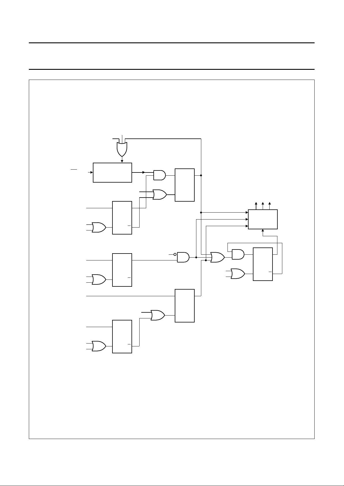
6.6 Interrupts
External, I2C-bus/derivative and timer/event counter
interrupts are handled by the PCF84CxxxA family.
The interrupt mechanism is single level, i.e. an executing
interrupt routine cannot be pre-empted unless by reset.
Further interrupt requests are latched. If several interrupt
requests are detected simultaneously, they are honoured
according to their priority:
• External interrupt (highest priority)
• I2C-bus/derivative interrupt
• Timer/event counter interrupt (lowest priority).
An interrupt request is only sensed if the corresponding
enable flag is set (see Fig.7). When the request is
honoured, the contents of the Program Counter and bits
4, 6 and 7 of the Program Status Word are saved on the
Program Counter stack. The Program Counter is loaded
with the appropriate interrupt vector, thereby indicating the
beginning of the interrupt routine. Since the Accumulator is
not automatically saved, it must be saved and restored by
user software. The interrupt routine must be terminated by
the RETR (return and restore) instruction. At least one
instruction of the main program will then be executed
before another interrupt routine is entered. To avoid
erroneous real-time programs, a few words of caution:
• While the interrupt is in progress, the two most
significant bits of the Program Counter are frozen at
zero. Thus, interrupt routines and subroutines called
from interrupt routines must reside entirely in bank 0.
• The SEL MB instruction must not be used in interrupt
routines and in subroutines called from interrupt
routines. Otherwise, the changed contents of MBFF0
and MBFF1 (see Fig.6) may lead to erroneous JMP and
CALL destinations after return from interrupt.
• Subroutines and nested subroutines called from the
interrupt routine must all end with RET since RETR
clears the Interrupt In Progress flag (IIP), as a side-effect
(see Figs 7 and 8). Further pending interrupts would
then interfere with the interrupt routine in progress.
6.6.1 E
XTERNAL INTERRUPT
A HIGH-to-LOW transition on the INT/T0 pin is latched in
the digital filter/latch if the LOW state exceeds 7 clock
periods after a HIGH state of more than 4 clock periods.
If the external interrupt is enabled the External Interrupt
Flag (EIF) is also asserted, thus constituting a valid
external interrupt request. As soon as the IIP is clear,
indicating that no interrupt routine is in progress, the
external interrupt is invoked by a forced CALL to
location 3. The EIF is simultaneously cleared (see
Figs 7 and 8). The interrupt routine may acknowledge the
interrupt via port lines. Execution of a DIS I (disable
external interrupt) instruction cancels a stored interrupt
request by clearing both the digital filter/latch and the EIF.
6.6.1.1 Interrupt/Test 0 (INT/T0)
The INT/T0 input has two purposes:
• External interrupt input
• Test 0 input.
When used as a Test 0 input (external interrupt disabled)
the conditional branch instruction JT0 will cause a jump if
INT/T0 = 1. The conditional branch instruction JNT0 will
also cause a jump if
INT/T0 = 0. If INT/T0 is not used, it
must be tied to VDD or VSS.
6.6.2 I
2
C-BUS/DERIVATIVE INTERRUPT
The I2C-bus/derivative interrupt is shared between the
I2C-bus interface (if available) and the derivative logic (if
available). Software polling may be necessary to
determine the origin of a request.
An interrupt condition in the I2C-bus interface and/or the
derivative logic will pull the PIN line LOW. If the
I2C-bus/derivative interrupt is enabled and no interrupt
routine is in progress, the I2C-bus/derivative interrupt
routine will be invoked by a forced CALL to program
memory location 5. The I2C-bus/derivative interrupt
routine must include instructions that will remove the
cause of the I2C-bus/derivative interrupt and thus reset
PIN to its inactive HIGH state (for further details see
Section 6.9). For derivative interrupts, consult the data
sheet of the specific device.
6.6.3 T
IMER/EVENT COUNTER INTERRUPT
If the timer/event counter interrupt is enabled, a
timer/event counter 1 overflow sets the Timer Interrupt
Flag (TIF). As soon as IIP is clear, meaning that no
interrupt routine is in progress, the timer/event counter
interrupt routine is invoked by a forced CALL to program
memory location 7. The TIF is simultaneously cleared (see
Figs 7 and 8). Execution of a DIS TCNTI (disable
timer/event counter interrupt) instruction cancels a stored
interrupt request by clearing TIF.
The timer/event counter interrupt may also be used to
simulate a second external interrupt. After an enable
timer/event counter interrupt (EN TCNTI), the counter
mode is enabled by a STRT CNT instruction which loads
FFH (the state preceding overflow) into the counter.
A positive edge on the T1 pin will overflow the counter and
set TIF.
1996 Nov 22 9
Page 10
Philips Semiconductors Product specification
8-bit microcontrollers PCF84CxxxA family
RESET
handbook, full pagewidth
DIS I
CLEAR
INT / T0
EN I
DIS I
RESET
EN SI
DIS SI
RESET
TIMER
OVERFLOW
EN
TCNT I
DIS
TCNT I
RESET
DIGITAL
FILTER / LATCH
CLEAR EIF
SQ
EI
ENABLE
R
SQ
SI
ENABLE
R
CLEAR TIF
SQ
TI
ENABLE
R
Q
Q
Q
PIN
SQ
EIF
R
SQ
TIF
R
MBA285 - 1
RETR
RESET
CALL EI / CLEAR EIF
CALL SI
CALL TI / CLEAR TIF
INTERRUPT
VECTOR
LOGIC
SQ
IIP
R
Q
Fig.7 Simplified interrupt logic schematic (the R input overrules the S input for all flags).
1996 Nov 22 10
Page 11
Philips Semiconductors Product specification
8-bit microcontrollers PCF84CxxxA family
handbook, full pagewidth
RESET
FETCH
INSTRUCTION
RETR?
Y
CLEAR IIP
AND RETURN
TO MAIN PROGRAM
N
EN I?
OR
EN TCNT I?
OR
EN SI?
Y
ENABLE
RELEVANT
INTERRUPT
TIMER
OVERFLOW?
N
INT / TO
N
EIF
SET?
N
Y
Y
Y
DIS I?
Y
DISABLE EI
CLEAR FILTER
LATCH AND EIF
SET TF
TI
ENABLED?
N
N
DIS SI?
DISABLE
Y
SET FILTER
NN
DIS
TCNT I?
Y
SI
SET TIF
LATCH
Y
DISABLE TI
AND CLEAR
TIF
EXECUTE
INSTRUCTION
N
FILTER
LATCH
SET?
Y
SET?
PIN = 0?
TIF SET?
Y
N
IIP
N
YN
IIP
SET?
Y
N
N
Y
N
SI
ENABLED?
SET IIP
CLEAR TIF
CALL 007 CALL 005
ENABLED
Y
SET IIP
YN
EI
SET EIF
CLEAR FILTER
LATCH
SET IIP
CLEAR EIF
CALL 003
MLA695
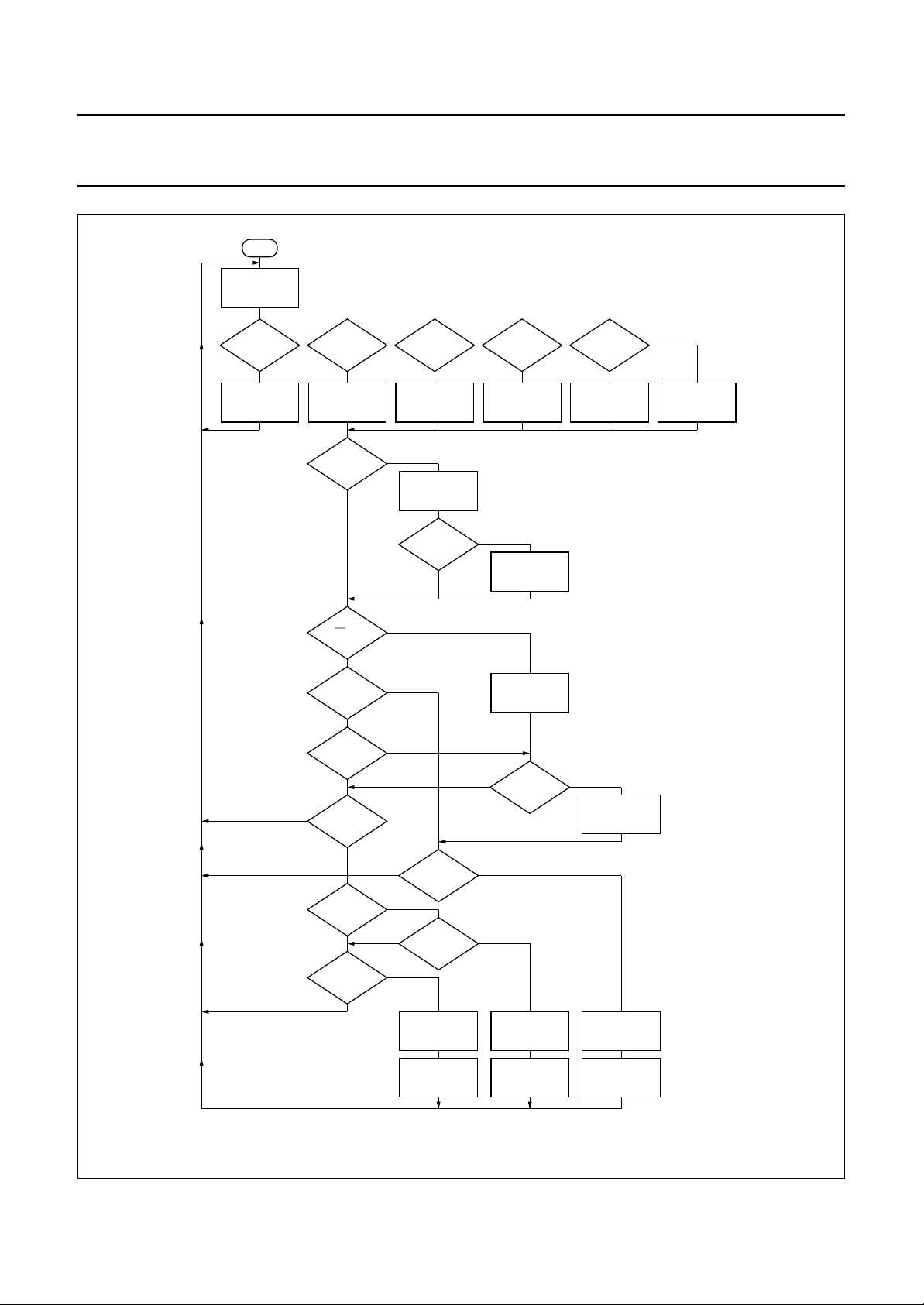
Fig.8 Flow chart illustrating CPU control in the presence of interrupts.
1996 Nov 22 11
Page 12
Philips Semiconductors Product specification
8-bit microcontrollers PCF84CxxxA family
6.7 Timer/event counter 1
An internal 8-bit up counter is provided. The counter can
be preset and read by the MOV T, A and MOV A, T
instructions.
When the counter is to be used in the timer mode,
a STRT T (start timer) instruction must be executed.
Depending on the PS bit in the Program Status Word,
the counter will increment every machine cycle (PS = 1,
1
⁄30× f
) or every 32 machine cycles (PS = 0,1⁄
xtal
960
× f
xtal
STRT T clears the prescaler (see Fig.9) which is not
otherwise accessible.
To count external events a STRT CNT (start event
counter) instruction must be executed. A LOW-to-HIGH
transition on pin T1 is counted if the HIGH state exceeds
4 clock periods after a LOW state of more than 4 clock
periods. The maximum count rate is one increment per
machine cycle (
⁄30× f
xtal
).
1
The timer mode and the event counter mode are both
inhibited after reset or by executing a STOP TCNT (stop
timer/event counter) instruction (see Fig.9).
In both the timer and in event counter modes, overflow has
two effects:
• If the timer/event counter interrupt is enabled TIF is
asserted thereby generating a timer/event counter
interrupt request (see Section 6.6).
• The Timer Flag (TF) is set. TF can be tested by
conditional branch instructions JTF (jump if TF = 1) or
JNTF (jump if TF = 0). The JTF and JNTF instruction, as
).
a side-effect, reset TF. The only other way to clear TF is
to reset the microcontroller.
6.7.1 TEST 1/COUNT INPUT (T1)
The T1 input has two purposes:
• Count input of 8-bit timer/event counter 1 (see
Section 6.7)
• Test 1 input.
When used as a Test 1 input the conditional branch
instruction JT1 will cause a jump if T1 = 1. The conditional
branch instruction JNT1 will also cause a jump if T1 = 0.
If T1 is not used, it must be tied to VDD or VSS.
handbook, full pagewidth
T1
f
30
xtal
PS = 1 PS = 0
EDGE
DETECTOR
A: STRT T
B: STRT CNT
C: STOP TCNT
STRT T
CLEAR
PRESCALER
.
.
32
MOV T, A
MOV A, T
A
B
C
8-BIT
TIMER /
EVENT
COUNTER
CLEAR
RESET
Fig.9 Timer/event counter 1.
timer overflow
RESET
SQ
R
SQ
R
JTF, JNTF
TIF
TF
interrupt
logic
conditional
branch logic
MBA294
1996 Nov 22 12
Page 13

Philips Semiconductors Product specification
8-bit microcontrollers PCF84CxxxA family
6.8 Parallel ports
Three standard quasi-bidirectional I/O ports are defined:
• Port 0: parallel port of 8 lines (P0.0 to P0.7)
• Port 1: parallel port of 8 lines (P1.0 to P1.7)
• Port 2: parallel port of 4 lines (P2.0 to P2.2, SDA/P2.3).
Several members of the PCF84CxxxA family provide all
20 port lines. The eight Port 0 lines (P0.0 to P0.7) are
available as a minimum. In addition to the standard ports,
many PCF84CxxxA microcontrollers offer a variety of
derivative ports. Please consult the data sheet of the
specific device.
In general, all parallel ports can be used as either inputs or
outputs. Output data written to a port is latched and
remains unchanged until rewritten. If the port is used as an
input, the external data is not latched and must remain
stable until it is accessed by the CPU.
The standard port configuration is illustrated in Fig.11.
When a logic 0 is written to the master/slave flip-flop, TR2
and TR3 are both in the OFF condition. TR1 turns ON and
drives the output to V
When a logic 1 is written to the master/slave flip-flop, TR1
turns OFF. TR2 and TR3 both turn ON driving the output
rapidly to VDD. TR2 remains in the ON condition for the
duration of the write pulse only. The constant current
source is responsible for keeping the output line high.
Sufficient source current is available for a TTL load HIGH
level; the line can, however, be overridden by an external
device. This is used when the port line serves as an input,
but it may also be useful for wired-OR applications. In the
latter case, unnecessary current through external devices
is avoided since repeated logic 1 write operations will not
activate TR2. The booster transistor TR2 is only asserted
during a LOW-to-HIGH transition of the master/slave
flip-flop. If the port line is to be used as an input, a logic 1
should first be stored in the master/slave flip-flop to turn
TR1 OFF.
Access to Ports 0, 1 and 2 is provided by the parallel
input/output instructions IN, OUTL, ANL and ORL.
IN inputs port data to the Accumulator. OUTL outputs
Accumulator data to the port. ANL and ORL are used for
data manipulation in the port flip-flop. In contrast to Ports
0, 1 and 2, derivative ports are accessed by the derivative
input/output instructions MOV, ANL and ORL. ANL and
ORL are used for data manipulation in the port flip-flop.
MOV is used for all data transfers between port and
Accumulator. The source data for the Accumulator can be
loaded from either the port line or the port flip-flop.
Two derivative addresses are therefore provided per port
(see Table 2).
SS
.
All standard and derivative port accesses are performed
by two-cycle instructions. Their instruction timing is shown
in Fig.11. For input, data on port lines is sensed during
timeslots 3 and 4 of machine cycle 2 (see Sections 6.10
and 6.11). For output, the data change occurs in
timeslot 7. For OUTL, data changes during machine
cycle 1. For ANL, ORL and MOV Dx, A, data changes
during machine cycle 2.
Table 2 Derivative port address pair
ADDRESS TYPE ACCESS
8-bit line address R derivative port line
8-bit flip-flop address R/W derivative port flip-flop
Three mask-programmable options for port output
configuration are available:
Option 1 Standard Port; quasi-bidirectional I/O with
switched pull-up current source of 100 µA (typ.)
and p-channel booster transistor TR2. TR2 is
only active for 1 clock cycle during
LOW-to-HIGH transitions (see Fig.11).
Option 2 Open-drain; quasi-bidirectional I/O with only an
n-channel open drain output. Application as an
output requires connection of an external pull-up
resistor (see Fig.12). If unused, an option 2
output should be tied to V
input path from floating, thereby avoiding
undesirable current flow through input stages.
Option 3 Push-pull; drive capability of the output will be
5 mA (typ.) at VDD= 3 V in both polarities. Since
short circuit currents would flow during input,
push-pull lines must only be used as outputs
(see Fig.13).
If available, SDA/P2.3 is shared between the I2C-bus
interface and the parallel Port 2. Therefore, only the
open-drain configuration is permitted for SDA/P2.3.
For the remaining standard port lines (P0.0 to P2.2), all
three options are generally available.
Besides port output mask options, the port flip-flop state,
after reset, may be specified for each individual port line
(except SDA/P2.3). Usually the ‘set option’ will be
selected, which avoids short-circuits for ports intended as
inputs. However, there may be cases in which the port
should output a logic zero after reset. The user may then
specify the ‘reset option’ for certain port lines.
. This keeps the
SS
1996 Nov 22 13
Page 14

Philips Semiconductors Product specification
8-bit microcontrollers PCF84CxxxA family
handbook, full pagewidth
time slot
P0, P1, P2, Dx
P0, P1, P2
P0, P1, P2, Dx
cycle 1
1234567891012345678910
DATA OUT
DATA
IN
cycle 2
DATA OUT
MLA615
Fig.10 Input /output timing of standard and derivative ports.
IN A, P
p
OUTL P , A
p
ANL P , #data, ORL P , #data
ANL Dx, A, ORL Dx, A
MOV Dx, A (flip-flop address)
pp
handbook, full pagewidth
WRITE PULSE
OUTL / ORL / ANL / MOV
DATA BUS
D
MQ
MASTER
ORL / ANL / MOV
D
SLAVE
SQ
SQ
IN / MOV
Fig.11 Standard output with switched current source.
1996 Nov 22 14
TR2
TR1
V
constant
current
TR3
V
SS
source
100 µA typ.
MLA696
DD
I/O PORT
LINE
Page 15

Philips Semiconductors Product specification
8-bit microcontrollers PCF84CxxxA family
handbook, full pagewidth
WRITE PULSE
OUTL / ORL / ANL
DATA BUS
D
MQ
MASTER
ORL / ANL
D
SLAVE
Fig.12 Open drain output.
SQ
SQ
IN
TR1
V
DD
V
SS
MLA697
I/O PORT
LINE
handbook, full pagewidth
WRITE PULSE
OUTL / ORL / ANL
DATA BUS
D
MQ
MASTER
ORL / ANL
D
SLAVE
Fig.13 Push-pull output.
1996 Nov 22 15
SQ
V
TR2
TR1
V
SS
IN
DD
I/O PORT
LINE
MLA698
Page 16

Philips Semiconductors Product specification
8-bit microcontrollers PCF84CxxxA family
6.9 I2C-bus interface
Many members of the PCF84CxxxA family have a serial
I/O interface - the I2C-bus or ‘Inter-Integrated Circuit Bus’.
This two-line serial bus extends the microcontroller
capabilities when implemented with the powerful I2C-bus
devices. Details of these devices can be found in
Handbook IC12, I2C Peripherals”
.
“Data
Microcontrollers that do not have a I2C-bus interface can
simulate it by software, by using port pins. However, such
microcontrollers must continuously monitor the serial bus.
As well as degrading the maximum data transfer rate, this
approach may also consume significant processing and
memory resources.
If available, however, the I2C-bus interface detects the
valid 7-bit I2C-bus address of the device, transfers serial
data and provides data conversion to and from parallel
format, all without disrupting program execution. When a
complete byte has been transferred, an interrupt is
requested by which the next data byte can be written to or
read out of the I2C-bus interface. The I2C-bus interface
also facilitates the implementation of multimaster systems
in which two or more microcontrollers communicate via the
same I2C-bus. An automatic arbitration procedure
resolves bus conflicts.
The I2C-bus consists of a bidirectional clock line (SCL) and
a bidirectional data line (SDA). Whereas SCL uses the
dedicated pin SCLK, SDA and Port line P2.3 share the pin,
SDA/P2.3. When the I2C-bus interface is enabled,
SDA/P2.3 is disabled as a port line. Input signals on SCLK
and SDA are filtered for enhanced noise immunity. When
used as outputs, SCLK and SDA/P2.3 require an external
pull-up resistor because they are open drain. If unused,
SCLK and SDA/P2.3 should be tied to VSS (see
Section 6.8, Option 2, Open-drain output).
Communication between CPU and I2C-bus interface is
handled through the four I2C-bus interface registers S0,
S0’, S1 and S2 (see Fig.14).
6.9.1 D
ATA SHIFT REGISTER (S0)
The data shift register converts serial data to a parallel
format and vice versa. The leading bit of a serial transfer
corresponds to the most significant bit of the parallel word.
An interrupt request is issued after transfer of a complete
byte and after detection of the valid I2C-bus address.
Register S0 is read by MOV A, S0. It is written by
MOV S0, A or MOV S0, #data if the ESO (Enable Serial
I/O) bit in the Status Register (S1) is set.
6.9.2 A
DDRESS REGISTER (S0’)
The address register contains the 7-bit I2C-bus address of
the device and the ALS (Always Selected) bit. When ALS
is zero, which is the recommended mode of operation, bus
transfers are ignored unless the valid device address
immediately follows the start condition. Besides the stored
7-bit address, the ‘general call address’ (pre-defined as
zero) is also acceptable as a valid address. If ALS is set,
however, any transfer on the bus will be stored in the data
shift register.
The address register S0’ is write-only. It can be written by
MOV S0, A and MOV S0, #data if the ESO (Enable Serial
I/O) bit in the Status Register (S1) is zero.
6.9.3 C
The Clock Control Register defines the frequency of f
LOCK CONTROL REGISTER (S2)
SCLK
as the microcontroller clock frequency divided by an
integer (see Table 3). It also defines ASC (Asymmetrical
Clock) and ACK (Acknowledge).
If ASC = 1, the generated SCLK has a duty cycle of
approximately 75%. The asymmetrical clock limits the
I2C-bus transmission rate to below 55 kHz. Divisors 39, 45
and 51 are not allowed if ASC = 1. However, an SCLK duty
cycle of approximately 50% results if ASC = 0. This
permits I2C-bus transmission rates of up to 100 kHz.
All divisors of Table 3 are available. It is, therefore,
recommended to select ASC = 0.
A detailed description of the I2C-bus specification, with
applications, is given in the brochure
how to use it”
. This brochure may be ordered using the
code 9398 393 40011. Data handbook IC12,
Peripherals”
also contains this information, and data on all
“The I2C-bus and
“I2C
current I2C-bus slave devices.
1996 Nov 22 16
For the normal I2C-bus protocol ACK must be set. After
each byte transfer an extra SCLK pulse is generated
during which the receiver may acknowledge reception.
If ACK is zero, no acknowledge phase is available. This
mode is temporarily used when a master/receiver refuses
the acknowledgement in order to signal an end of
transmission to the slave transmitter (see Section 6.9.4.9).
The Clock Control Register (S2) is write-only. It can be
written by MOV S2, A and MOV S2, #data.
Page 17

Philips Semiconductors Product specification
8-bit microcontrollers PCF84CxxxA family
book, full pagewidth
SDA/P2.3
SCLK
DIGITAL FILTER
DIGITAL FILTER
ADDRESS REGISTER S0'
A6 A5 A4 A3 A2 A1 A0 ALS
MSB
DATA SHIFT REGISTER S0
MSB
ARBITRATION
AND
SYNCHRONIZATION
LOGIC
CLOCK CONTROL REGISTER S2
X ACK ASC CC4 CC3 CC2 CC1 CC0
MSB
STATUS REGISTER S1
MSB
7
ADDRESS COMPARATOR
7
CLOCK
GENERATOR
ESO
PINBBTRXMST
AASAL AD0
8
LSB
D0D1D2D3D4D5D6D7
8
LSB
8
8
LSB
8
BC0
BC1BC2
LRB
LSB
MLA699
INTERNAL BUS
8
Fig.14 Block diagram of the I2C-bus interface.
1996 Nov 22 17
Page 18

Philips Semiconductors Product specification
8-bit microcontrollers PCF84CxxxA family
Table 3 f
CC4 TO CC0
(HEX)
0A 171 20.9 58.5 93.6
0B 195 18.4 51.3 82.1
0C 243 14.7 41.2 65.8
0D 291 12.3 34.4 55.0
0E 339 10.6 29.5 47.2
0F 387 9.2 25.8 41.3
1A 2691 1.3 3.7 5.9
1B 3075 1.2 3.3 5.2
1C 3843 0.9 2.6 4.2
1D 4611 0.8 2.2 3.5
1E 5379 0.7 1.9 3.0
1F 6147 0.6 1.6 2.6
as defined by Clock Control Register (S2)
SCLK
f
(kHz) at
f
DIVISOR
xtal
(Division Factor)
f
= 3.58 MHz f
xtal
SCLK
= 10 MHz f
xtal
= 16 MHz
xtal
00 forbidden −−−
01 39 91.8 256.4
02 45 79.5 222.2
03 51 70.2 196.1
04 63 56.8 158.7
05 75 47.7 133.3
06 87 41.1 114.9
07 99 36.2 101.0
(1)
(1)
(1)
(1)
(1)
(1)
(1)
08 123 29.1 81.3 130.1
09 147 4.4 68.0 108.8
410.3
355.6
313.7
254.0
213.3
183.9
161.6
(1)
(1)
(1)
(1)
(1)
(1)
(1)
(1)
(1)
10 483 7.4 20.7 33.1
11 579 6.2 17.3 27.6
12 675 5.3 14.8 23.7
13 771 4.6 13.0 20.8
14 963 3.7 10.4 16.6
15 1155 3.1 8.7 13.9
16 1347 2.7 7.4 11.9
17 1539 2.3 6.5 10.4
18 1923 1.9 5.2 8.3
19 2307 1.6 4.3 6.9
Note
1. Not permitted; maximum f
= 100 kHz in I2C-bus systems.
SCLK
1996 Nov 22 18
Page 19

Philips Semiconductors Product specification
8-bit microcontrollers PCF84CxxxA family
6.9.4 STATUS REGISTER (S1)
The Status Register controls the I2C-bus interface and
provides feedback concerning on-going bus transfers.
Register S1 can be accessed by MOV A, S1; MOV S1, A
and MOV S1, #data. The lower nibble of the Status
Register is twofold: control bits BC0, BC1, BC2 and ESO
can only be written, whereas feedback bits LRB, AD0, AAS
and AL can only be read. Table 4 describes the status bits.
The status bits interact in intricate ways with each other.
This must be kept in mind when an I2C-bus application is
programmed.
6.9.4.1 Master bit (MST) and Transmitter bit (TRX)
MST and TRX together define the state of the I2C-bus
interface. When not engaged in a bus transfer MST and
TRX should always be at zero, the slave/receiver state
(see Fig.15). Return to this state is always performed by
software. If the previous state was the master state, the
transition (to slave/receiver by MOV1, #D8H) involves a
stop condition which, as a consequence, clears both MST
and TRX.
The transition to the master/transmitter state is also a
programmed event. However, transitions to the
master/receiver and the slave/transmitter states occur
automatically if ALS = 0 (standard I2C-bus protocol).
A slave/receiver becomes a slave/transmitter if R/W = 1 in
its valid address (following the start condition). A
master/transmitter becomes a master/receiver if R/W=1
in the transmitted address.
6.9.4.2 Pending Interrupt Not bit (PIN)
If MST = 1 or, if ALS = 1, PIN is set to zero after every byte
transfer. Conversely, PIN becomes zero when a valid
address is detected and after each byte of the following
transfer. In addition, the serial interrupt request, PIN = 0
initiates ‘clock synchronization’, i.e. the SCLK line is pulled
to VSS as long as PIN = 0. With this feature a slave may
slow down a master, thus providing time to read the Data
Register (in the case of a slave/receiver) or to write to the
data register (in the case of a slave/transmitter). PIN is
cancelled by an access to register S0 or by explicitly
setting PIN to one.
If the I2C-bus/derivative interrupt is disabled, the I2C-bus
interface may be serviced by testing PIN directly in user
software.
6.9.4.3 Bus Busy bit (BB)
The Bus Busy bit (BB) is controlled by the I2C-bus
interface or by software in the bus master to generate the
start and stop conditions. When a master clears BB (by
MOV S1, #D8H), the I2C-bus interface automatically
clears MST and TRX, thereby returning to the
slave/receiver state (see Fig.15). If BB = 1, write access to
S1 is inhibited, except for the master or an addressed
slave. Should BB be inadvertently set by excessive noise
on the bus, the deadlock can be resolved by two
consecutive MOV S1, #18H, the first of which just clears
BB.
When a slave/transmitter detects an end of transmission
(signalled by the lack of an acknowledgment from the
master receiver), it has to access S1 in order to cancel PIN
and to become slave/receiver. However, BB should
remain set. This is reflected by MOV S1, #38H as
illustrated in Fig.15. With PIN = 1, ‘clock synchronization’
terminates, enabling the master to generate the stop
condition.
A start condition must only be generated when BB = 0;
otherwise the I
arbitration has been lost (see Section 6.9.4.4).
2
C-bus interface will respond as if bus
6.9.4.4 Arbitration Lost bit (AL)
The AL bit is set by the I2C-bus interface when it loses a
bus arbitration in the master/transmitter mode. MST and
TRX are cleared simultaneously to enable the interface,
now in slave/receiver mode, to determine if it is validly
addressed by the device that won the arbitration. PIN is
activated when the byte transfer is complete. AL will be
cleared when the serial interrupt is cancelled.
6.9.4.5 Addressed As Slave bit (AAS)
AAS is set by the I2C-bus interface following a start
condition when the valid address is detected (ALS = 0 in
register S0’) or when the first byte is received (ALS = 1 in
register S0’). AAS is cleared when the serial interrupt is
cancelled.
6.9.4.6 Address Zero bit (AD0)
AD0 is set, independently of ALS, by the I2C-bus interface
when byte 00H, the 'general call' address, is detected
following a start condition. AD0 is cleared after a repeated
start or a stop condition.
1996 Nov 22 19
Page 20

Philips Semiconductors Product specification
8-bit microcontrollers PCF84CxxxA family
6.9.4.7 Last Received Bit (LRB)
LRB corresponds to the last bit transferred. If ACK = 1,
LRB contains the acknowledgement bit. It remains valid as
long as PIN = 0.
6.9.4.8 Enable Serial I/O bit (ESO)
When ESO = 0 access to register S0' is enabled. SCLK is
in the high-impedance state and SDA/P2.3 is available as
a normal port line.
When ESO = 1 the I2C-bus interface and access to
register S0 is enabled. Only when ESO = 1 may the other
bits of register S1 be changed. SCLK and SDA/P2.3 are
enabled as serial clock and data lines, respectively.
To avoid bus deadlock, ESO must be set to zero prior to
the execution of the STOP instruction.
Table 4 Overview of Status Register bits
BIT NAME TYPE DESCRIPTION
MST Master R/W MST = 0: slave (SCLK input).
MST = 1: master (SCLK output).
TRX Transmitter TRX = 0: receiver (SDA/P2.3 input.
TRX = 1: transmitter (SDA/P2.3 output).
BB Bus Busy R/W BB = 0: bus inactive (R)/generates stop condition (W).
BB = 1: bus busy (R)/generates start condition (W).
PIN Pending Interrupt Not R/W PIN = 0: serial interrupt pending (after byte transfer, valid address or
lost arbitration). SCLK line forced to V
PIN = 1: no serial interrupt pending.
ESO Enable Serial Output W ESO = 0: I
ESO = 1: I2C-bus interface enabled write access to S0 possible.
BC0 to
BC2
AL Arbitration Lost R Set: when a bus conflict is lost.
AAS Addressed As Slave R Set: following a start condition if valid address is detected (ALS = 0)
AD0 Address zero R Set: following a start condition if byte 00H (‘general call’ address) is
LRB Last Received Bit R Set or Reset depending on the value of the last bit transferred,
Bit Counter 0 to 2 W 3-bit binary value of 0 to 7, counting down the number of bits
transferred (0 used for complete byte).
Reset: when corresponding serial interrupt (PIN) is cancelled.
or if first byte is received (ALS = 1).
Reset: when corresponding serial interrupt (PIN) is cancelled.
detected.
Reset: after a repeated start or a stop condition.
acknowledgement bit if ACK = 1.
6.9.4.9 Bit Counter bits (BC0, BC1 and BC2)
The bit counter bits BC0, BC1 and BC2 should all be at
zero for normal I2C-bus operation. The bit counter is
always cleared by a start condition. Therefore, all eight bits
of the first byte are transferred.
If a non-zero bit counter value is chosen, it is only valid for
one register S0 transfer since the counter decrements to
zero. An important use of the bit counter arises when a
master/receiver signals an end of transmission by sending
a negative acknowledge after the last byte received. To do
this, the last byte is received with bit ACK = 0 in
register S2. The negative acknowledge is then issued by
setting the bit counter to one and ‘receiving’ one bit from
the HIGH level available on the SDA line.
The slave/transmitter interprets the same signals as a
negative acknowledgement.
.
SS
2
C-bus interface disabled/write access to S0' possible.
1996 Nov 22 20
Page 21

Philips Semiconductors Product specification
8-bit microcontrollers PCF84CxxxA family
handbook, full pagewidth
SLAVE
TRANSMITTER
MOV SI, #38H(R/W = 1) and (ALS = 0)
SLAVE
RECEIVER
MOV SI, #D8H MOV SI, #F8H
MOV SI, #D8H
MASTER
RECEIVER
(R/W = 1) and (ALS = 0)
Fig.15 State diagram of the I2C-bus interface.
6.10 Timing
Every machine cycle consists of 10 time slots which are
again subdivided into 3 clock periods each (see Fig.16).
Permitted clock frequencies range from 1 MHz to a
maximum, which is a function of the supply voltage.
At VDD≥ 4.5 V, a 16 MHz maximum clock frequency is
guaranteed.
handbook, full pagewidth
1 2 3 4 5 6 7 8 9 10
machine cycle
MASTER
TRANSMITTER
programmed transition
automatic transition
MBA298 - 1
The clock signal may be internally generated by an on-chip
oscillator. Alternatively, an external clock may be applied
to pin XTAL1. In this configuration, a short circuit with an
internal pull-up transistor on XTAL1 may occur while the
oscillator is inhibited (see Section 6.11). Care should be
taken to avoid excessive current flow.
10 time slots
30 clock periods
Fig.16 Timing of a machine cycle.
1996 Nov 22 21
MBA296
Page 22

Philips Semiconductors Product specification
8-bit microcontrollers PCF84CxxxA family
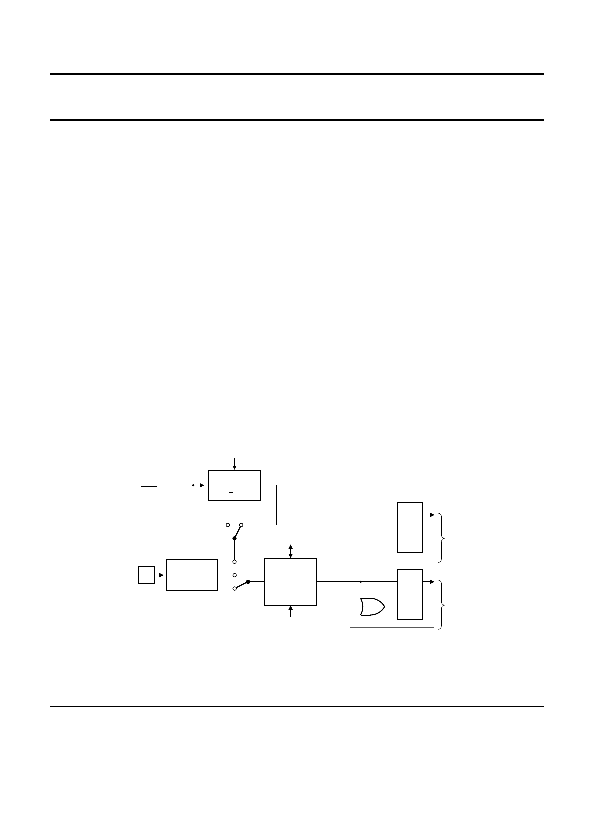
6.11 Oscillator
The on-chip oscillator basically consists of an inverter
stage which includes a feedback resistor and load
capacitors (see Fig.17). In most applications, a quartz
crystal will be connected between XTAL1 and XTAL2.
Alternatively, a ceramic resonator or an inductor may be
used as a timing element.
When the supply voltage drops below the power-on
reference level, the oscillator is inhibited. The internal
oscillator can also be inhibited by the STOP instruction
under software control (see Section 6.13.2 ).
The transconductance (g
) of the inverter stage can be
m
mask-programmed, thereby optimizing the oscillator for a
specific frequency and resonator. Three standard
transconductance options, referred to as LOW, MEDIUM
and HIGH, can be specified by the user.
With C1=C2= 10 pF on-chip, external capacitors are not
required for quartz oscillators. However, for adequate
frequency stability, PXE resonators need external
capacitors in the order of the static resonator capacitance
C0, such as external C1=C2= 30 to 100 pF.
C1 C2
XTAL1 XTAL2
inhibit
g
m
C
R
F
F
MLA614
Oscillator start-up time depends mainly on the external
timing element. The start-up time of a quartz crystal is
several milliseconds because of the narrow crystal
bandwidth. For proper oscillator start-up, the
transconductance (gm) of the inverter stage must fulfil
relationship (1); shown below.
Table 5 Notation to relationship (see Figs 17 and 18)
SYMBOL DEFINITION
R
C
R
R
R
C
C
resonator series resistance
X
static resonator capacitance
0
resonator loss resistance
0
R0 // R
P
F
L
F
F
feedback resistor
C1 × C2/(C1 + C2) (load capacitance)
parasitic feedback capacitance (typically
2 pF on-chip, external value depends on
printed-circuit board wiring)
ω 2πf
4.2 RXω2CLC0C
osc
2
1
++()
+ g
-------
F
R
P
<<
------------------------------------------------------------------
m
C1 C2×
R
XC0CF
+()
handbook, halfpage
2
1
+
--------------
2
ω
Fig.17 Oscillator with integrated elements.
R
MBA295 - 1
symbol
C
0
Fig.18 Crystal unit equivalent circuit.
R
P
C
X
L
X
0
R
X
(1)
1996 Nov 22 22
Page 23

Philips Semiconductors Product specification
8-bit microcontrollers PCF84CxxxA family
6.12 Reset
To ensure proper start-up, the microcontroller must be
initialized to a defined starting condition. The device
executes the first instruction 1866 clock cycles after the
falling edge of the internal reset.
6.12.1 P
ASSIVE EXTERNAL RESET
A passive reset is generated by the RC circuit illustrated in
Fig.19. While VDD rises, the discharged C
keeps the
reset
RESET pin near the VDD level. When VDD crosses the
power-on reference level (V
) the power-on reset circuit
ref
generates a reset pulse of approximately 50 µs. This pulse
is without effect since it feeds into the reset signal forced
by the one on the RESET pin. The f
dependent
xtal
minimum VDD must be reached before the voltage on
RESET drops below V
lower bound for C
= 0.7VDD. This translates into a
IH
resetRreset
equal to twice the rise time of
VDD (for linearly rising VDD) or eight times the time constant
of VDD (for exponentially rising VDD). The internal diode
rapidly discharges C
when VDD falls off, ensuring
reset
reliable reset even after short interruptions of supply
voltage. To avoid overload of the internal diode, an
external diode should be added in parallel if
C
> 2.2 µF.
reset
6.12.2 A
CTIVE EXTERNAL RESET
An active reset can be generated by driving the RESET pin
HIGH from an external logic device. Such an active reset
pulse should not fall off before VDD has reached its
f
dependent minimum operating value.
xtal
handbook, full pagewidth
C
reset
R
reset
100 kΩ
V
DD
RESET
V
POR
POWER-ON-RESET
Fig.19 Passive external reset
internal reset
≈ 50 µs
oscillator inhibit
MLA700
1996 Nov 22 23
Page 24

Philips Semiconductors Product specification
8-bit microcontrollers PCF84CxxxA family
6.12.3 INTERNAL RESET
In systems where VDD reaches its f
operating value before the clock f
dependent minimum
xtal
is applied, reset can
xtal
be performed without external components. This condition
is generally fulfilled with quartz and PXE resonators since
oscillator start-up takes several milliseconds. Besides,
rapid power-up is usually available in battery-powered
systems.
If the internal power-on reset is used the RESET pin
should be connected to VSS. When VDD increases above
the power-on reference level V
, the power-on-reset
ref
circuit generates a reset pulse of approximately 50 µs.
This pulse guarantees proper initialization under the
conditions defined above.
The power-on reference level V
is a mask option.
ref
The user can select a reference voltage between 1.2 V
and 3.6 V in discrete steps of 100 mV. The accuracy of the
reference voltage is ±500 mV for the V
3.0 V and ±800 mV for the V
The chosen V
should have sufficient margin regarding
ref
range 3.1 V to 3.6 V.
ref
range 1.2 V to
ref
the minimum intended VDD.
A mask option without an internal power-on reset circuit is
also available. It is recommended if the user does not
intend to use the internal power-on-reset circuit. In this
case, the supply current requirements in Stop mode
(see Section 6.13.2) will reduce to the level of leakage
currents, i.e. virtually zero at ambient temperature.
6.12.4 R
ESET STATE
After a reset, the device state is characterized as follows:
• Program Counter 0
• Memory bank 0
• Register bank 0 - Stack Pointer 0 (location pair 8 and 9)
• All interrupts disabled
• Timer/event counter 1 stopped and cleared
• Timer prescaler modulo-32 (PS = 0)
• Timer flag cleared
• All port flip-flops (except SDA/P2.3) set to 1 (set option)
or 0 (reset option) as selected by the user
• SDA/P2.3 is high-impedance with the port flip-flop set
to 1
• SCLK is high-impedance
2
C-bus interface disabled (ESO = 0) and in
• I
slave/receiver mode (S0, S0’, S1 and S2 cleared except
for PIN = 1)
• Idle and Stop modes cancelled.
1996 Nov 22 24
Page 25

Philips Semiconductors Product specification
8-bit microcontrollers PCF84CxxxA family
6.13 Reduced power modes
6.13.1 I
DLE MODE
The Idle mode is very useful in low-power applications.
When all computational tasks are completed, the device
can be put into standby instead of into a busy waiting loop.
Nevertheless, the device is on the alert and ready to
respond rapidly to any interrupt.
The microcontroller enters the Idle mode via the IDLE
instruction. In the Idle mode, all activity is halted except for
the oscillator, the timer/event counter 1 and the I2C-bus
interface (if available).
The microcontroller leaves the Idle mode when an enabled
interrupt occurs. The interrupt routine is executed before
operation resumes with the instruction following the IDLE
opcode.
handbook, full pagewidth
normal mode
PROGRAM
FLOW
IDLE
Idle mode
For timer/event counter interrupts and I
2
C-bus/derivative
interrupts, termination of the Idle mode is straightforward.
However, care must be taken when the Idle mode is left by
the external interrupt since INT/T0 is negative-edge
responding. If INT/T0 was LOW prior to entering the Idle
mode, it must be taken HIGH before the negative edge can
be generated. Figure 20 specifies the exact timing for
leaving the Idle mode via the external interrupt INT/T0.
If no interrupt is enabled, the Idle mode can only be
terminated by an active signal on the RESET pin. A normal
reset sequence is executed (see Fig.20).
program counter =
0 or 003H
normal mode
XTAL2
INT/T0
or
RESET
clock
periods
t
RESET
1 µs
clock
periods
clock
periods
1866
clock periods
760
4
Fig.20 Entering and leaving the Idle mode.
(PC) = 0003H
(PC) = 0000H
MLA702
1996 Nov 22 25
Page 26

Philips Semiconductors Product specification
8-bit microcontrollers PCF84CxxxA family
6.13.2 STOP MODE
The Stop mode allows very low-power applications. When
all computational tasks are completed, the device can be
almost completely shut off by stopping its oscillator. In
contrast to the Idle mode, the device is not ready to
respond rapidly to any interrupt.
The microcontroller enters the Stop mode via the STOP
instruction. The oscillator is switched off. All internal states
and I/O levels are maintained.
The microcontroller leaves the Stop mode by a LOW level
INT/T0 or a reset. In the latter case, a normal reset
on
sequence is executed (see Fig.21).
handbook, full pagewidth
normal mode
PROGRAM
FLOW
XTAL2
STOP
In contrast to the Idle mode and the external interrupt
mechanism, the microcontroller responds to a LOW level
INT/T0 rather than to a negative edge. IfINT/T0 is LOW
on
when the STOP instruction is executed, the Stop mode will
not be entered.
A negative edge on INT/T0 continues program execution
after a 1866 clock cycle delay, which ensures proper
oscillator start-up. If the external interrupt is enabled, the
device executes the instruction following the STOP
opcode before diverting to the interrupt routine. If the
external interrupt is disabled, program execution continues
with the instructions following the STOP opcode (see
Fig.21).
normal modeStop mode
INT/T0
or
RESET
t
INT
1 µs
1866
clock
periods
t
RESET
1 µs
don't care
1866
clock
periods
Fig.21 Entering and leaving the Stop mode.
(PC) = address
following STOP
(PC) = 0000H
MLA701
1996 Nov 22 26
Page 27

Philips Semiconductors Product specification
8-bit microcontrollers PCF84CxxxA family
6.14 Derivative logic
Derivative logic is provided with many members of the
PCF84CxxxA family. The detailed description of the
derivative circuitry is given in the data sheet of the specific
device. In this section, the shared principles of derivative
logic are briefly reviewed.
Derivative registers are accessed over the internal bus.
The derivative registers are write-only, read-only or
handbook, full pagewidth
8
DERIVATIVE ADDRESS REGISTER
DECODER
8
8
DERIVATIVE WRITE REGISTER
DERIVATIVE READ REGISTER
read/write (see Fig.22). They are addressed through the
derivative address register when the derivative
input/output instructions (MOV A, Dx; MOV Dx, A;
ANL Dx, A and ORL Dx, A) are executed.
Derivative interrupts share the line PIN with the I
interrupt (if available). When the derivative interrupt
routine is executed, the PIN line must be de-activated by
software.
8
256
PIN
DERIVATIVE
INTERRUPT
LOGIC
2
C-bus
8
DERIVATIVE READ / WRITE REGISTER
INTERNAL
BUS
MBA297
Fig.22 Block diagram of derivative logic.
Table 6 Summary of mask options
FEATURE OPTION DESCRIPTION
ROM any mix of instructions program; size restricted by ROM size (see Tables 7 and 8)
Ports option 1 standard output (see Fig.11)
option 2 open drain output (see Fig.12)
option 3 push-pull output (see Fig.13)
set flip-flop at logic 1 after reset
reset flip-flop at logic 0 after reset
Oscillator g
mL
g
mM
g
mH
LOW transconductance
MEDIUM transconductance
HIGH transconductance
1996 Nov 22 27
Page 28

Philips Semiconductors Product specification
8-bit microcontrollers PCF84CxxxA family
7 INSTRUCTION SET
The PCF84CxxxA instruction set consists of over 100 one and two-byte instructions. Program code efficiency is high
because all RAM locations and all ROM locations on a 256-byte page require only a single-byte address. Table 8 lists
the symbols that are used in Table 7 and the Instruction map is shown in Section 7.1.
Table 7 PCF84CxxxA family instruction set
MNEMONIC
OPCODE
(HEX)
BYTES/
CYCLES
DESCRIPTION FUNCTION NOTES
ACCUMULATOR
ADD A, Rr
ADD A, @Rr
ADD A, #data
ADDC A, Rr
ADDC A, @Rr
(1)
6<8 + r> 1/1 Add register contents to A (A)←(A) + (Rr) r = 0 to 7
(1)
6r 1/1 Add RAM data, addressed by Rr, to A (A)←(A) + ((Rr)) r = 0, 1
(1)
03 data 2/2 Add immediate data to A (A)←(A) + data
(1)
7<8 + r> 1/1 Add carry and register contents to A (A)←(A) + (Rr) + (C) r = 0 to 7
(1)
7r 1/1 Add carry and RAM data, addressed by
(A)←(A) + ((Rr)) + (C) r = 0, 1
Rr, to A
(1)
ADDC A, #data
13 data 2/2 Add carry and immediate data to A (A)←(A) + data + (C)
ANL A, Rr 5<8 + r> 1/1 AND Rr with A (A)←(A) AND (Rr) r = 0 to 7
ANL A, @Rr 5r 1/1 AND RAM data addressed by Rr, with A (A)←(A) AND ((Rr)) r = 0, 1
ANL A, #data 53 data 2/2 AND immediate data with A (A)←(A) AND data
ORL A, Rr 4<8 + r> 1/1 OR Rr with A (A)←(A) OR (Rr) r = 0 to 7
ORL A, @Rr 4r 1/1 OR RAM data, addressed by Rr, with A (A)←(A) OR ((Rr)) r = 0, 1
ORL A, #data 43 data 2/2 OR immediate data with A (A)←(A) OR data)
XRL A, Rr D<8 +r> 1/1 XOR Rr with A (A)←(A) XOR (Rr) r = 0 to 7
XRL A, @Rr Dr 1/1 XOR RAM data, addressed by Rr, with A (A)←(A) XOR ((Rr)) r = 0, 1
XRL A, #data D3 data 2/2 XOR immediate data with A (A)←(A) XOR data)
INC A 17 1/1 Increment A by 1 (A)←(A) + 1
DEC A 07 1/1 Decrement A by 1 (A)←(A) − 1
CLR A 27 1/1 Clear A to zero (A)←0
CPL A 37 1/1 One’s complement A (A)←NOT(A)
RL A E7 1/1 Rotate A left (A
n +1
)←(An),
n = 0 to 6
(A0)←(A7)
RLC A
(2)
F7 1/1 Rotate A left through carry (A
n +1
)←(An),
n = 0 to 6
(A0)←(C), (C)←(A7)
RR A 77 1/1 Rotate A right (A
)←(A
n
n +1
),
n = 0 to 6
(A7)←(A0)
RRC A
(2)
67 1/1 Rotate A right through carry (An)←(A
n + 1
),
n = 0 to 6
(A7)←(C), (C)←(A0)
DA A
(2)
57 1/1 Decimal adjust A (A)←(A) + 06H if
AC = 1 or (A
0-3
)>9;
(A)←(A) + 60H if
(A
)>9
4-7
SWAP A
(2)
47 1/1 Swap nibbles of A (A
4-7
)↔(A
0-3
)
1996 Nov 22 28
Page 29

Philips Semiconductors Product specification
8-bit microcontrollers PCF84CxxxA family
MNEMONIC
OPCODE
(HEX)
BYTES/
CYCLES
DESCRIPTION FUNCTION NOTES
DATA MOVES
MOV A, Rr F<8 + r> 1/1 Move register contents to A (A)←(Rr) r = 0 to 7
MOV A, @Rr Fr 1/1 Move RAM data addressed by Rr, to A (A)←((Rr)) r = 0, 1
MOV A, #data 23 data 2/2 Move immediate data to A (A)←data
MOV Rr, A A<8 + r> 1/1 Move Accumulator contents to register (Rr)←(A) r = 0 to 7
MOV@Rr, A Ar 1/1 Move Accumulator contents to RAM
((Rr))←(A) r = 0, 1
location addressed by Rr
MOV Rr, #data B<8 + r>
2/2 Move immediate data to Rr (Rr)←data r = 0 to 7
data
MOV @Rr, #data Br data 2/2 Move immediate data to RAM location
((R0))←data r = 0, 1
addressed by Rr
XCH A, Rr 2<8 + r> 1/1 Exchange A contents with Rr (A)↔(Rr) r = 0 to 7
XCH A, @Rr 2r 1/1 Exchange Accumulator contents with
(A)↔((Rr)) r = 0, 1
RAM data addressed by Rr
XCHD A, @Rr 3r 1/1 Exchange lower nibbles of A and RAM
(A
)↔((Rr
0-3
)) r = 0, 1
0-3
data addressed by Rr
MOV A, PSW C7 1/1 Move PSW contents to Accumulator (A)←(PSW)
(3)
MOV PSW, A
MOV P A, @A A3 1/2 Move indirectly addressed data in
D7 1/1 Move Accumulator bit 3 to PSW3 (PS) (PS)←(A3)
)←(A),
(PC
0-7
current page to A
(A)←((PC))
CARRY FLAG
(2)
CLR C
CPL C
(2)
97 1/1 Clear carry bit (C)←0
A7 1/1 Complement carry bit (C)←NOT(C)
REGISTER
INC Rr 1<8 + r> 1/1 Increment register by 1 (Rr)←(Rr) + 1 r = 0 to 7
INC @Rr 1r 1/1 Increment RAM data, addressed by Rr,
((Rr))←((Rr)) + 1 r = 0, 1
by 1
DEC Rr C<8 + r> 1/1 Decrement register by 1 (Rr)←(Rr) − 1 r = 0 to 7
DEC @Rr Cr 1/1 Decrement RAM data addressed by Rr,
((Rr))←((Rr)) − 1 r = 0, 1
by 1
1996 Nov 22 29
Page 30

Philips Semiconductors Product specification
8-bit microcontrollers PCF84CxxxA family
MNEMONIC
OPCODE
(HEX)
BYTES/
CYCLES
DESCRIPTION FUNCTION NOTES
BRANCH
JMP addr <2n>4
addr
2/2 Unconditional jump within a 2 kbyte
bank
(PC
(PC
(PC
8-10
)←addr
0-7
11-12
)←n
)←
(MBFF0-1)
JMPP @A B3 1/2 Indirect jump within a page (PC
DJZN Rr, addr E<8 + r>
addr
2/2 Decrement Rr by 1 and jump if not zero
to addr
DJNZ @Rr, addr Er 2/2 Decrement RAM data, addressed by Rr,
by 1 and jump if not zero to addr
JBb addr <2b + 1>
2/2 Jump to addr if Accumulator bit b = 1 If (A
2 addr
)←((A))
0-7
(Rr)←(Rr) − 1;
if (Rr) not zero, then
)←addr
(PC
0-7
((Rr))←((Rr)) − 1;
if ((Rr)) not zero, then
(PC
)←addr
0-7
) = 1, then
b
(PC
)←addr
0-7
JC addr F6 addr 2/2 Jump to addr if C = 1 If (C) = 1, then
)←addr
(PC
0-7
JNC addr E6 addr 2/2 Jump to addr if C = 0 If (C) = 0, then
)←addr
(PC
0-7
JZ addr C6 addr 2/2 Jump to addr if A = 0 If (A) = 0,
)←addr
(PC
0-7
JNZ addr 96 addr 2/2 Jump to addr if A is NOT zero If (A) ≠ 0, then
)←addr
(PC
0-7
JT0 addr 36 addr 2/2 Jump to addr if T0 = 1 If T0 = 1, then
)←addr
(PC
0-7
JNT0 addr 26 addr 2/2 Jump to addr if T0 = 0 If T0 = 0, then
)←addr
(PC
0-7
JT1 addr 56 addr 2/2 Jump to addr if T1 = 1 If T1 = 1, then
)←addr
(PC
0-7
JNT1 addr 46 addr 2/2 Jump to addr if T1 = 0 If T0 = 0, then
)←addr
(PC
0-7
JTF addr
JNTF addr
(4)
(4)
16 addr 2/2 Jump to addr if Timer Flag = 1 If TF = 1, then
(PC
)←addr
0-7
06 addr 2/2 Jump to addr if Timer Flag = 0 If T0 = 0, then
(PC
)←addr
0-7
n = 0 to 7
r=0to7
r=0to1
b = 0 to 7
1996 Nov 22 30
Page 31

Philips Semiconductors Product specification
8-bit microcontrollers PCF84CxxxA family
MNEMONIC
OPCODE
(HEX)
BYTES/
CYCLES
DESCRIPTION FUNCTION NOTES
TIMER/EVENT COUNTER
MOV A,T 42 1/1 Move timer/event counter contents to A (A)←(T)
MOV T, A 62 1/1 Move A contents to timer/event counter (T)←(A)
STRT CNT 45 1/1 Start event counter
STRT T 55 1/1 Start timer
STOP TCNT 65 1/1 Stop timer/event counter
EN TCNTI 25 1/1 Enable timer/event counter interrupt
DIS TCNTI 35 1/1 Disable timer/event counter interrupt
CONTROL
EN I 05 1/1 Enable external (chip enable) interrupt
DIS I 15 1/1 Disable external (chip enable) interrupt
SEL RB0
SEL RB1
SEL MB0
(5)
(5)
(10)
C5 1/1 Select register bank 0 (RBS)←0
D5 1/1 Select register bank 1 (RBS)←1
E5 1/1 Select program memory bank 0 (MBFF0)←0,
(MBFF1)←0
SEL MB1
(10)
F5 1/1 Select program memory bank 1 (MBFF0)←1,
(MBFF1)←0
SEL MB2
(10)
A5 1/1 Select program memory bank 2 (MBFF0)←0,
(MBFF1)←1
SEL MB3
(10)
B5 1/1 Select program memory bank 3 (MBFF0)←1,
(MBFF1)←1
STOP 22 1/1 Enter Stop mode
IDLE 01 1/1 Enter Idle mode
SUBROUTINE
CALL addr
(6)
<2n + 1>
2/2 Jump to subroutine ((SP))←(PC)
4addr
(6)
RET
RETR
(6)
83 1/2 Return from subroutine (SP)←(SP) − 1,
93 1/2 Return from interrupt and restore bits 4,
6 and 7 of PSW
1996 Nov 22 31
(PSW
4,6,7
),
(SP)←(SP) + 1,
(PC
(PC
(PC
)←n,
8-10
)←addr,
0-7
11-12
)
←(MBFF0-1)
(PC)←((SP))
(SP)←(SP) − 1,
(PSW
4,6,7
) +
(PC)←((SP))
n = 0 to 7
Page 32

Philips Semiconductors Product specification
8-bit microcontrollers PCF84CxxxA family
MNEMONIC
OPCODE
(HEX)
BYTES/
CYCLES
DESCRIPTION FUNCTION NOTES
PARALLEL INPUT/OUTPUT
IN A, P0 08 1/2 Input Port 0 data to Accumulator (A)←(P0)
IN A, P1 09 1/2 Input Port 1 data to Accumulator (A)←(P1)
IN A, P2
(7)
0A 1/2 Input Port 2 data to Accumulator (A)←(P2)
OUTL P0, A 38 1/2 Output A data to Port 0 (P0)←(A)
OUTL P1, A 39 1/2 Output A data to Port 1 (P1)←(A)
OUTL P2, A 3A 1/2 Output A data to Port 2 (P2)←(A)
ANL P0, #data 98 data 2/2 AND Port 0 data with immediate data (P0)←(P0) AND data
ANL P1, #data 99 data 2/2 AND Port 1 data with immediate data (P1)←(P1) AND data
ANL P2, #data 9A data 2/2 AND Port 2 data with immediate data (P2)←(P2) AND data
ORL P0, #data 88 data 2/2 OR Port 0 data with immediate data (P0)←(P0) OR data
ORL P1, #data 89 data 2/2 OR Port 1 data with immediate data (P1)←(P1) OR data
ORL P2, #data 8A data 2/2 OR Port 2 data with immediate data (P2)←(P2) OR data
DERIVATIVE INPUT/OUTPUT
MOV A, Dx
MOV Dx, A
ANL Dx, A
ORL Dx, A
(8)
(8)
(8)
(8)
SERIAL INPUT/OUTPUT (I
MOV A, S0 0C 1/2 Move I
MOV A, S1
(9)
MOV S0, A 3C 1/2 Move A contents to I
MOV S1, A
(9)
MOV S2, A 3E 1/2 Move A contents to I
MOV S0, #data 9C data 2/2 Move immediate data to I
8C direct 2/2 Move derivative register contents to A (A)←(Dx) x = 0 to
8D direct 2/2 Move A contents to derivative register (Dx)←(A) x = 0 to
8E direct 2/2 AND derivative register with A (Dx)←(Dx) AND (A) x = 0 to
8F direct 2/2 OR derivative register with A (Dx)←(Dx) OR (A) x = 0 to
2
C-bus operations)
2
C-bus register 0 contents to A (A)←(S0)
0D 1/2 Move I2C-bus register 1 contents to A (A)←(S1)
2
C-bus register 0 (S0)←(A)
3D 1/2 Move A contents to I2C-bus register 1 (S1)←(A)
2
C-bus register 2 (S2)←(A)
2
C-bus register0(S0)←data
255
255
255
255
MOV S1, #data
MOV S2, #data 9E data 2/2 Move immediate data to I
(9)
9D data 2/2 Move immediate data toI2C-bus register1(S1)←data
2
C-bus register2(S2)←data
EN SI 85 1/1 Enable serial I/O interrupt
DIS SI 95 1/1 Disable serial I/O interrupt
NOP 00 1/1 No operation (PC
(PC
1996 Nov 22 32
0-10
0-10
)←
) + 1
Page 33

Philips Semiconductors Product specification
8-bit microcontrollers PCF84CxxxA family
Notes to Table 7
1. PSW CY, AC affected.
2. PSW CY affected.
3. PSW PS affected.
4. Execution of a JTF or JNTF instruction resets the Timer Flag (TF).
5. PSW RBS affected.
6. PSW SP0, SP1 and SP2, affected.
7. (A) = 0000, P2.3, P2.2, P2.1 and P2.0.
8. For more information on the derivative I/O instructions of a particular microcontroller, consult the specific
microcontroller data sheet.
9. (S1) has a different meaning for read and write operations. See Section 6.9.4.
10. SEL MB instructions may not be used within interrupt routines.
1996 Nov 22 33
Page 34

Philips Semiconductors Product specification
8-bit microcontrollers PCF84CxxxA family
Table 8 Definitions of symbols used in Table 7
SYMBOL DESCRIPTION
A Accumulator
AC auxiliary (half) carry
addr program memory address
Bb bit designation (b = 0 to 7)
CE/T0 CE/T0 input
CY carry bit
Dx mnemonic derivative register
data 8-bit number or expression
MB0 program memory bank 0
MB1 program memory bank 1
MB2 program memory bank 2
MB3 program memory bank 3
MBFF0 memory bank flip-flop 0
MBFF1 memory bank flip-flop 1
PC Program Counter
PS timer prescaler select
PSW Program Status Word
RB0 register bank 0
RB1 register bank 1
RBS register bank select
Rr register designation (r = 0 to 7)
SPn Stack Pointer (n = 0, 1 or 2)
T Timer 1
T1 T1 input
TF Timer Flag
x derivative register address (x = 0 to 255)
(X) contents of X
((X)) contents of location addressed by X
← is replaced by
↔ is exchanged with
# immediate data prefix
@ indirect address prefix
* hexadecimal; 8...F selects R0...R7
& hexadecimal; 0, 2, 4, 6, 8, A, C, E
selects page 0...7 in JMP,
i.e. (PC
% hexadecimal; 1, 3, 5, 7, 9, B, D, F
selects page 0...7 in CALL,
i.e. (PC
selects bit b = 0...7 in JBb,
i.e. b = &
8-10
8-10
1-3
)←&
)←&
1-3
1-3
1996 Nov 22 34
Page 35

Philips Semiconductors Product specification
8-bit microcontrollers PCF84CxxxA family
7.1 Instruction map
handbook, full pagewidth
first hexadecimal character of opcode second hexadecimal character of opcode
0123456789ABCDEF
NOP IDLE
0
INC @ Rr
1
01
XCH A, @Rr
2
0
XCHD A, @Rr
3
0
ORL A, @Rr
4
0
ANL A, @Rr
5
0
ADD A, @Rr
6
01
ADDC A, @Rr
7
0
8
9
MOV @ Rr,A
A
0
MOV @Rr, #data
B
0
DEC @Rr
C
0
XRL A, @Rr
D
01
DJNZ @ Rr,addr
E
01
MOV A, @Rr
F
01
STOP
1
1
1
1
addr
1
1
1
1
JB0
addr
JB1
addr
MOV
A, T
JB2
addr
MOV
T, A
JB3
JB4
addr
JB5
addr
JB6
addr
JB7
addr
ADD
A, #data
ADDC
A,#data
MOV
A, #data
A, #data
A, #data
RETR
MOVP
A,@A
JMPP
A,#data
ORL
ANL
RET
@A
XRL
JMP
page 0
CALL
page 0
JMP
page 1
CALL
page 1
JMP
page 2
CALL
page 2
JMP
page 3
CALL
page 3
JMP
page 4
CALL
page 4
JMP
page 5
CALL
page 5
JMP
page 6
CALL
page 6
JMP
page 7
CALL
page 7
EN I
DIS I
EN
TCNTI
DIS
TCNTI
STRT
CNT
STRT
T
STOP
TCNT
EN
SI
DIS
SI
SEL
MB2
SEL
MB3
SEL
RB0
SEL
RB1
SEL
MB0
SEL
MB1
JNTF
addr
JTF
addr
JNT0
addr
JT0
addr
JNT1
addr
JT1
addr
JNZ
addr
JZ
addr
JNC
addr
JC
addr
DEC A
INC A
CLR A
CPL A
SWAP
A
DA A
RRC A
RR A
CLR C
CPL C
MOV
A,PSW
MOV
PSW,A
RL A
RLC A
IN A,Pp MOV A,Sn
0
12
0
1
0
1
OUTL Pp,A
0
1
0
1
0
1
0
1
0
1
ORL Pp,#data
0
1
ANL Pp,#data MOV Sn,#data
1
0
0
1
0
1
0
1
0
1
0
1
01
34567
2
34567
2
2
2
34567
2
34567
2
34567
34567
2
2
2
2
345
MOV Rr,#data
2
34567
3
2
2
3
2
3
2
34
01
INC Rr
XCH A,Rr
01 2
ORL A,Rr
ANL A,Rr
ADD A,Rr
ADDC A,Rr
MOV
A,Dx
01 2
MOV Rr,A
DEC Rr
45
XRL A,Rr
4
DJNZ Rr,addr
4
MOV A,Rr
MOV Sn,A
MOV
Dx,A
5
5
56
6
67
6
6
ANL
Dx,A
ORL
Dx,A
7
7
7
7
MBA281
1996 Nov 22 35
Page 36

Philips Semiconductors Product specification
8-bit microcontrollers PCF84CxxxA family
8 DEFINITIONS
Data sheet status
Objective specification This data sheet contains target or goal specifications for product development.
Preliminary specification This data sheet contains preliminary data; supplementary data may be published later.
Product specification This data sheet contains final product specifications.
Limiting values
Limiting values given are in accordance with the Absolute Maximum Rating System (IEC 134). Stress above one or
more of the limiting values may cause permanent damage to the device. These are stress ratings only and operation
of the device at these or at any other conditions above those given in the Characteristics sections of the specification
is not implied. Exposure to limiting values for extended periods may affect device reliability.
Application information
Where application information is given, it is advisory and does not form part of the specification.
9 LIFE SUPPORT APPLICATIONS
These products are not designed for use in life support appliances, devices, or systems where malfunction of these
products can reasonably be expected to result in personal injury. Philips customers using or selling these products for
use in such applications do so at their own risk and agree to fully indemnify Philips for any damages resulting from such
improper use or sale.
10 PURCHASE OF PHILIPS I
Purchase of Philips I
components in the I2C system provided the system conforms to the I2C specification defined by
Philips. This specification can be ordered using the code 9398 393 40011.
2
C COMPONENTS
2
C components conveys a license under the Philips’ I2C patent to use the
1996 Nov 22 36
Page 37

Philips Semiconductors Product specification
8-bit microcontrollers PCF84CxxxA family
NOTES
1996 Nov 22 37
Page 38

Philips Semiconductors Product specification
8-bit microcontrollers PCF84CxxxA family
NOTES
1996 Nov 22 38
Page 39

Philips Semiconductors Product specification
8-bit microcontrollers PCF84CxxxA family
NOTES
1996 Nov 22 39
Page 40

Philips Semiconductors – a worldwide company
Argentina: see South America
Australia: 34 Waterloo Road, NORTH RYDE, NSW 2113,
Tel. +61 2 9805 4455, Fax. +61 2 9805 4466
Austria: Computerstr. 6, A-1101 WIEN, P.O. Box 213,
Tel. +43 1 60 101, Fax. +43 1 60 101 1210
Belarus: Hotel Minsk Business Center, Bld. 3, r. 1211, Volodarski Str. 6,
220050 MINSK, Tel. +375 172 200 733, Fax. +375 172 200 773
Belgium: see The Netherlands
Brazil: see South America
Bulgaria: Philips Bulgaria Ltd., Energoproject, 15th floor,
51 James Bourchier Blvd., 1407 SOFIA,
Tel. +359 2 689 211, Fax. +359 2 689 102
Canada: PHILIPS SEMICONDUCTORS/COMPONENTS,
Tel. +1 800 234 7381
China/Hong Kong: 501 Hong Kong Industrial Technology Centre,
72 Tat Chee Avenue, Kowloon Tong, HONG KONG,
Tel. +852 2319 7888, Fax. +852 2319 7700
Colombia: see South America
Czech Republic: see Austria
Denmark: Prags Boulevard 80, PB 1919, DK-2300 COPENHAGEN S,
Tel. +45 32 88 2636, Fax. +45 31 57 1949
Finland: Sinikalliontie 3, FIN-02630 ESPOO,
Tel. +358 9 615800, Fax. +358 9 61580/xxx
France: 4 Rue du Port-aux-Vins, BP317, 92156 SURESNES Cedex,
Tel. +33 1 40 99 6161, Fax. +33 1 40 99 6427
Germany: Hammerbrookstraße 69, D-20097 HAMBURG,
Tel. +49 40 23 53 60, Fax. +49 40 23 536 300
Greece: No. 15, 25th March Street, GR 17778 TAVROS/ATHENS,
Tel. +30 1 4894 339/239, Fax. +30 1 4814 240
Hungary: see Austria
India: Philips INDIA Ltd, Shivsagar Estate, A Block, Dr. Annie Besant Rd.
Worli, MUMBAI 400 018, Tel. +91 22 4938 541, Fax. +91 22 4938 722
Indonesia: see Singapore
Ireland: Newstead, Clonskeagh, DUBLIN 14,
Tel. +353 1 7640 000, Fax. +353 1 7640 200
Israel: RAPAC Electronics, 7 Kehilat Saloniki St, TEL AVIV 61180,
Tel. +972 3 645 0444, Fax. +972 3 649 1007
Italy: PHILIPS SEMICONDUCTORS, Piazza IV Novembre 3,
20124 MILANO, Tel. +39 2 6752 2531, Fax. +39 2 6752 2557
Japan: Philips Bldg 13-37, Kohnan 2-chome, Minato-ku, TOKYO 108,
Tel. +81 3 3740 5130, Fax. +81 3 3740 5077
Korea: Philips House, 260-199 Itaewon-dong, Yongsan-ku, SEOUL,
Tel. +82 2 709 1412, Fax. +82 2 709 1415
Malaysia: No. 76 Jalan Universiti, 46200 PETALING JAYA, SELANGOR,
Tel. +60 3 750 5214, Fax. +60 3 757 4880
Mexico: 5900 Gateway East, Suite 200, EL PASO, TEXAS 79905,
Tel. +9-5 800 234 7381
Middle East: see Italy
Netherlands: Postbus 90050, 5600 PB EINDHOVEN, Bldg. VB,
Tel. +31 40 27 82785, Fax. +31 40 27 88399
New Zealand: 2 Wagener Place, C.P.O. Box 1041, AUCKLAND,
Tel. +64 9 849 4160, Fax. +64 9 849 7811
Norway: Box 1, Manglerud 0612, OSLO,
Tel. +47 22 74 8000, Fax. +47 22 74 8341
Philippines: Philips Semiconductors Philippines Inc.,
106 Valero St. Salcedo Village, P.O. Box 2108 MCC, MAKATI,
Metro MANILA, Tel. +63 2 816 6380, Fax. +63 2 817 3474
Poland: Ul. Lukiska 10, PL 04-123 WARSZAWA,
Tel. +48 22 612 2831, Fax. +48 22 612 2327
Portugal: see Spain
Romania: see Italy
Russia: Philips Russia, Ul. Usatcheva 35A, 119048 MOSCOW,
Tel. +7 095 247 9145, Fax. +7 095 247 9144
Singapore: Lorong 1, Toa Payoh, SINGAPORE 1231,
Tel. +65 350 2538, Fax. +65 251 6500
Slovakia: see Austria
Slovenia: see Italy
South Africa: S.A. PHILIPS Pty Ltd., 195-215 Main Road Martindale,
2092 JOHANNESBURG, P.O. Box 7430 Johannesburg 2000,
Tel. +27 11 470 5911, Fax. +27 11 470 5494
South America: Rua do Rocio 220, 5th floor, Suite 51,
04552-903 São Paulo, SÃO PAULO - SP, Brazil,
Tel. +55 11 821 2333, Fax. +55 11 829 1849
Spain: Balmes 22, 08007 BARCELONA,
Tel. +34 3 301 6312, Fax. +34 3 301 4107
Sweden: Kottbygatan 7, Akalla, S-16485 STOCKHOLM,
Tel. +46 8 632 2000, Fax. +46 8 632 2745
Switzerland: Allmendstrasse 140, CH-8027 ZÜRICH,
Tel. +41 1 488 2686, Fax. +41 1 481 7730
Taiwan: PHILIPS TAIWAN Ltd., 23-30F, 66,
Chung Hsiao West Road, Sec. 1, P.O. Box 22978,
TAIPEI 100, Tel. +886 2 382 4443, Fax. +886 2 382 4444
Thailand: PHILIPS ELECTRONICS (THAILAND) Ltd.,
209/2 Sanpavuth-Bangna Road Prakanong, BANGKOK 10260,
Tel. +66 2 745 4090, Fax. +66 2 398 0793
Turkey: Talatpasa Cad. No. 5, 80640 GÜLTEPE/ISTANBUL,
Tel. +90 212 279 2770, Fax. +90 212 282 6707
Ukraine: PHILIPS UKRAINE, 4 Patrice Lumumba str., Building B, Floor 7,
252042 KIEV, Tel. +380 44 264 2776, Fax. +380 44 268 0461
United Kingdom: Philips Semiconductors Ltd., 276 Bath Road, Hayes,
MIDDLESEX UB3 5BX, Tel. +44 181 730 5000, Fax. +44 181 754 8421
United States: 811 East Arques Avenue, SUNNYVALE, CA 94088-3409,
Tel. +1 800 234 7381
Uruguay: see South America
Vietnam: see Singapore
Yugoslavia: PHILIPS, Trg N. Pasica 5/v, 11000 BEOGRAD,
Tel. +381 11 625 344, Fax.+381 11 635 777
For all other countries apply to: Philips Semiconductors, Marketing & Sales Communications,
Building BE-p, P.O. Box 218, 5600 MD EINDHOVEN, The Netherlands, Fax. +31 40 27 24825
© Philips Electronics N.V. 1996 SCA52
All rights are reserved. Reproduction in whole or in part is prohibited without the prior written consent of the copyright owner.
The information presented in this document does not form part of any quotation or contract, is believed to be accurate and reliable and may be changed
without notice. No liability will be accepted by the publisher for any consequence of its use. Publication thereof does not convey nor imply any license
under patent- or other industrial or intellectual property rights.
Internet: http://www.semiconductors.philips.com
Printed in The Netherlands 457021/1200/03/pp40 Date of release: 1996 Nov 22 Document order number: 9397 750 01087
 Loading...