

Page 1

INTEGRATED CIRCUITS
DATA SH EET
PCF5078
Power amplifier controller for GSM
and PCN systems
Product specification
File under Integrated Circuits, IC17
1999 Apr 12
Page 2
Philips Semiconductors Product specification
Power amplifier controller for GSM and
PCF5078
PCN systems
FEATURES
• Compatible with baseband interface family PCF5073x
• Two power sensor inputs
• Temperature compensation of sensor signal
• Active filter for DAC input
• Power Amplifier (PA) protection against mismatching
• Bias current source for detector diodes
• Generation of pre-bias level for PA at start of burst
(home position)
• Possibility to adapt home position by external
components
• Applicable for a wide range of silicon and GaAs power
amplifiers.
QUICK REFERENCE DATA
SYMBOL PARAMETER MIN. TYP. MAX. UNIT
V
DD
I
DD(tot)
T
amb
supply voltage 2.4 3.6 5.0 V
total supply current −−6mA
operating ambient temperature −40 − +85 °C
APPLICATIONS
• Global System for Mobile communication (GSM)
• Personal Communications Network (PCN) systems.
GENERAL DESCRIPTION
This CMOS device integrates an amplifier for the detected
RF voltage from the sensor, an integrator and an active
filter to build a PA control loop for cellular systems with a
small amount of passive components.
ORDERING INFORMATION
TYPE
NUMBER
PCF5078T TSSOP8 plastic thin shrink small outline package; 8 leads; body width 3.0 mm SOT505-1
NAME DESCRIPTION VERSION
PACKAGE
1999 Apr 12 2
Page 3
Philips Semiconductors Product specification
Power amplifier controller for GSM and
PCN systems
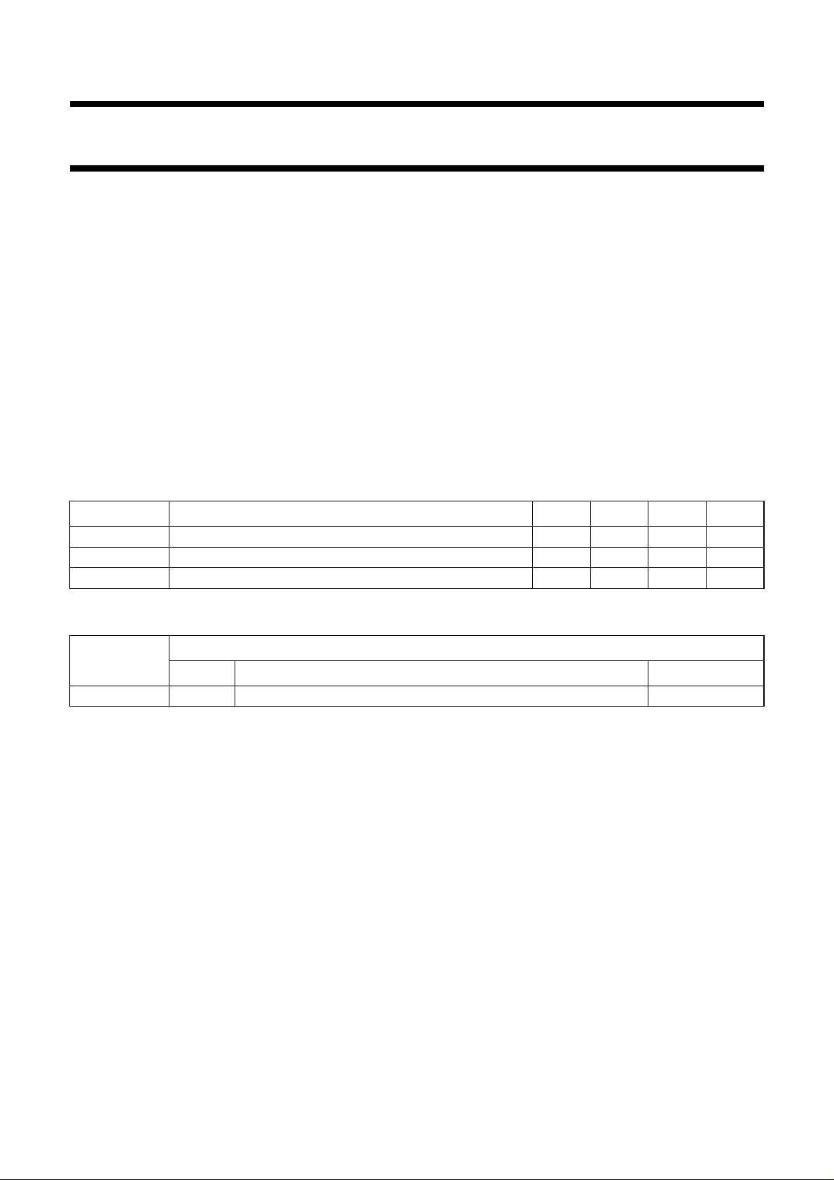
BLOCK DIAGRAM
handbook, full pagewidth
antenna
VS2 VS1 VC
3421
C1
6 pF
C2
6 pF
30 µA
V
V
DD
DD
C3
5 pF
56 7
SS
VDAC
VHOME
RF
PA
sensor
D1 D2
30 µA
V
S1
C4
10 pF
OP1
R6
15 kΩ
R3
50 kΩ
S5
PCF5078
V
DD
8
V
DD
R1
20 kΩ
10 µA
V
home
VINT
VDAC
PCF5078
R2
1 kΩ
V
S1
S2S2S3S3S4S4S5
CONTROL
LOGIC
DD
10 µA
V
prebias
R4
6 kΩ
MGS193
OP4
V
DD
AUXDAC3
PCF5073x
Fig.1 Block diagram.
1999 Apr 12 3
Page 4

Philips Semiconductors Product specification
Power amplifier controller for GSM and
PCN systems
PINNING
SYMBOL PIN DESCRIPTION
VC 1 PA control output voltage
VINT 2 negative integrator input
VS1 3 sensor signal input 1
VS2 4 sensor signal input 2
V
SS
VDAC 6 DAC input voltage
VHOME 7 home position input voltage
V
DD
handbook, halfpage
5 ground supply
8 supply voltage
VC
1
VINT VHOME
2
PCF5078
3
VS1
4
VS2
MGS194
8
7
6
5
V
DD
VDAC
V
SS
Fig.2 Pin configuration.
PCF5078
An external Digital-to-Analog Converter (DAC) with10-bit
resolution is necessary to control the loop e.g. the
AUXDAC3 of the baseband interface family PCF5073x.
An integrated active filter smooths the voltage steps of the
DAC and avoids a feedthrough of the DAC harmonics into
the modulation spectra of the PA.
The DAC signal and the sensor signal are added by
operational amplifier OP1. The voltage difference of both
signals is integrated by operational amplifier OP4, which
provides the PA control voltage on pin VC. The integration
is performed by means of an external capacitance C
connected between pins VINT and VC.
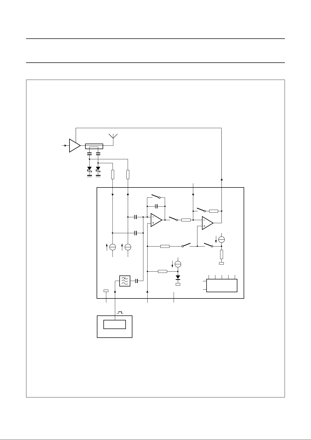
The shape of the rising and falling power burst edges can
be determined by means of the DAC voltage (see Fig.3).
Power-down mode
During the not used time slots in Time Division Multiple
Access (TDMA) systems, the PCF5078 must be turned off
by switching off the supply voltage on pin V
DD
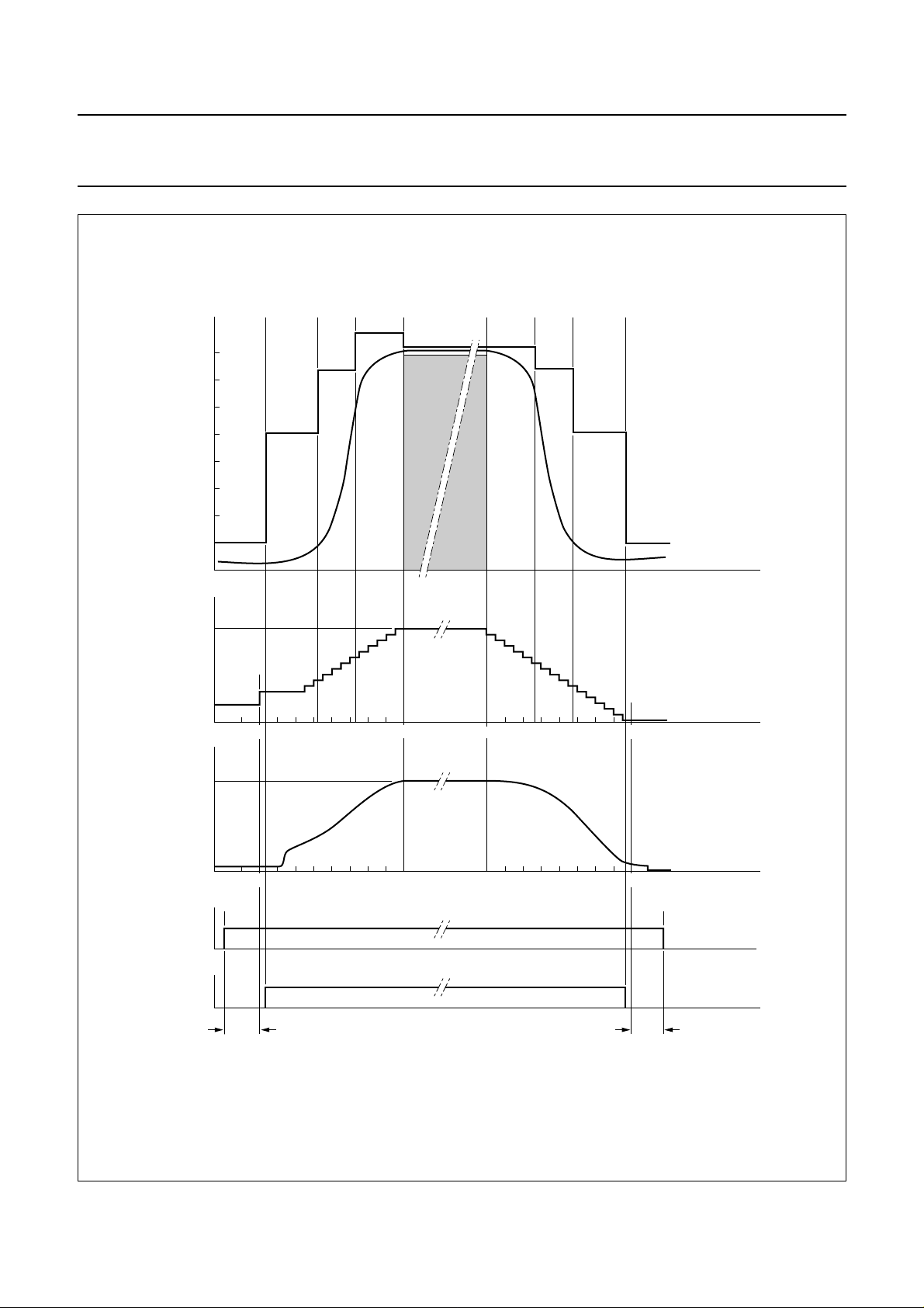
Initial conditions and start-up
The PCF5078 has been designed to operate in bursts as
required in TDMA systems. For each time slot to be
transmitted it must be powered-up by switching on the
supply voltage. This allows a proper initialization of
switches S1 to S5.
VINT
.
FUNCTIONAL DESCRIPTION
General
The PCF5078 integrates an amplifier for the detected RF
voltage from the sensor, an integrator and an active filter
to build a PA control loop with a small amount of passive
components.
The sensor amplifier is able to amplify signals from a RF
power detector in a range of −20 to +15 dBm. This
complies to the PA output power range of GSM and PCN
systems when a directional coupler with 20 dB attenuation
is used.
The Schottky diode for power detection (sensor) is biased
by an integrated current source of 30 µA. Variations of the
forward voltage of the diodes with the temperature have no
influence on the measured signal, because they are
cancelled by sampling around the switched capacitor
operational amplifier OP1 (see Fig.1).
During start-up switches S1, S2 and S3 are closed and
switches S4 and S5 are opened (see Fig.4).
The forward voltages on the Schottky diodes are sampled
on capacitors C1 and C2, respectively, because switch S1
is closed. Moreover, the control voltage on pin VC is
initially forced to pre-bias level V
prebias
because
switches S2 and S3 are closed and switch S4 is opened.
Switch S1 is opened after a fixed time the supply voltage
has been switched on and then the circuit is ready. This
time is defined on-chip and can be maximum 45 µs. Once
switch S1 is open, a ramp signal with a minimum
amplitude of 25 mV applied on pin VDAC determines
opening of switch S3 and closing of switch S4 with a delay
of maximum 3 µs with respect to the start of the ramp.
After opening switch S3, the control voltage on pin VC
rises in a fixed amount of time to the home position level
so biasing the PA to the beginning of the active range of its
control curve. Switch S2 remains closed during this typical
time of 2 µs. When switch S2 is opened, switch S5 is
closed allowing the transfer of any signal coming from
amplifier OP1.
1999 Apr 12 4
Page 5

Philips Semiconductors Product specification
Power amplifier controller for GSM and
PCN systems
After this preset, the control voltage is free to increase
according to the control loop if RF input is present
(see Fig.3).
For higher DAC ramp steps the delay time of opening
switch S3 (and closing switch S4) is reduced. On the
contrary, the delay time between opening switch S2 with
respect to opening switch S3 (and closing switch S4)
remains unchanged.
For a correct start-up it is required that the rising time of the
supply voltage is maximum 20 µs.
End of a burst
For a proper down ramp, the final value of the DAC input
voltage should be below the value at the beginning of the
burst and so be able to really shut-off the PA (see Fig.5).
This means the code programmed for the last bit of the
DAC down ramp (CODE
initial value of the up ramp (CODE
last code must be maintained until the supply voltage has
been switched off.
When the voltage on pin VC is detected to be lower than
V
to V
opening switches S4 and S5.
a built-in mechanism forces the voltage on pin VC
VHOME
by closing switches S1, S2 and S3 and by
prebias
) has to be lower than the
END
). Moreover, the
START
PCF5078
PA protection against mismatching
A second sensor amplified input is integrated into the
PCF5078 for measuring the reflected wave of the
directional coupler. The signal is added to the measured
RF power signal (see Fig.3). When mismatching at the
output of the PA occurs the power is reduced. A high
Voltage Standing W ave Ratio (VSWR) at the output of the
PA often occurs in systems where the PA is connected to
the antenna via switches with low attenuation instead of
using a duplex filter.
Home position voltage
A forward voltage of an on-chip silicon diode is provided as
the default home position voltage V
matches the requirements at the control input of most PAs
and exhibits the same temperature coefficient.
However, if another value is needed for a certain PA the
level can be adjusted by connecting external components
to pin VHOME (see Figs 10 and 11). The home position
voltage can be set between 200 and 1000 mV when using
a capacitor of 50 pF connected between pins VINT
and VC.
. This voltage
home
For proper operation, the supply voltage should be
switched off at least 15 µs later with respect to the end of
the down ramp on pin VDAC.
1999 Apr 12 5
Page 6
Philips Semiconductors Product specification
Power amplifier controller for GSM and
PCN systems
handbook, full pagewidth
0
RF
out
(dBc)
−10
−20
−30
−40
−50
−60
−70
V
VDAC
<0.9V
−80
DD
−28 −18 −10 0
+543 +553 +561 +571
PCF5078
time (µs)
CODE
START
<0.9V
V
prebias
V
V
RF
VC
DD
DD
CODE
END
1614121086420
1614121086420
in
32
3028262422201816
3028262422201816
DAC bits at 560 kHz
32
DAC bits at 560 kHz
>15 µs>45 µs
time
time
MGS197
Fig.3 Timing diagram.
1999 Apr 12 6
Page 7

Philips Semiconductors Product specification
Power amplifier controller for GSM and
PCN systems
handbook, full pagewidth
CODE
V
V
VDAC
START
closed
S1
opened
DD
<20 µs
<45 µs
>25 µs
>25 mV
0
<3 µs
PCF5078
time
42
6 . . .
DAC bits at 560 kHz
time
closed
opened
closed
opened
closed
opened
closed
opened
V
VHOME
V
prebias
S3
time
S4
time
S2
time
S5
2 µs
V
VC
MGS195
time
time
Fig.4 Initialization and start of a burst diagram.
1999 Apr 12 7
Page 8

Philips Semiconductors Product specification
Power amplifier controller for GSM and
PCN systems
handbook, full pagewidth
CODE
END
< CODE
V
V
VDAC
START
closed
DD
PCF5078
time
3028. . . 26
32
≥15 µs
DAC bits at 560 kHz
S1, S2, S3
opened
closed
S4, S5
opened
V
VC
V
VHOME
V
prebias
<12 µs
MGS196
time
time
time
Fig.5 End of a burst diagram.
1999 Apr 12 8
Page 9

Philips Semiconductors Product specification
Power amplifier controller for GSM and
PCF5078
PCN systems
LIMITING VALUES
In accordance with the Absolute Maximum Rating System (IEC 134).
SYMBOL PARAMETER MIN. MAX. UNIT
V
DD
V
n
I
n
P
tot
T
stg
T
amb
CHARACTERISTICS
V
= 2.4 to 5 V; T
DD
SYMBOL PARAMETER CONDITIONS MIN. TYP. MAX. UNIT
Supply
V
DD
I
DD(tot)
Sensor input voltage
V
I(n)
Bias current source
I
bias
TC
bias
supply voltage 2.4 6.0 V
DC voltage on
pins VS2 and VS2 −3.0 +6.0 V
all other pins −0.5 +6.0 V
DC current on any signal pin −10 +10 mA
total power dissipation − 315 mW
storage temperature −65 +150 °C
operating ambient temperature −40 +85 °C
= −40 to +85 °C; see Fig.1; unless otherwise specified.
amb
supply voltage 2.4 3.6 5.0 V
total supply current −−6mA
input voltage on pins VS1 and VS2 −3 − V
DD
V
detector diode bias current no input signal;
T
=25°C; see Fig.7
amb
V
=2.4V 172839µA
DD
V
=5.0V 213345µA
DD
temperature coefficient of bias current
− 0.07 −µA/K
source
Home position voltage
V
TC
home
home
internal home position voltage T
temperature coefficient of internal home
amb
position voltage source
R3 resistor for internal home position
voltage
V
I(VHOME)
home position input voltage 200 − 1000
Low pass filter for DAC signal (3rd-order Bessel)
f
3dB
corner frequency 70 100 130 kHz
1999 Apr 12 9
=25°C 0.550 0.600 0.650 V
−−2.1 − mV/K
− 50 − kΩ
(1)
mV
Page 10

Philips Semiconductors Product specification
Power amplifier controller for GSM and
PCF5078
PCN systems
SYMBOL PARAMETER CONDITIONS MIN. TYP. MAX. UNIT
Integrator (OP4)
B
G
PSRR power supply rejection ratio at 217 Hz; V
SR
pos
SR
neg
V
O(min)
V
O(max)
Capacitors C1, C2, C3 and C4
M matching ratio accuracy between
Notes
1. For C
2. Guaranteed by design.
3. Slew rates are measured between 10% and 90% of output voltage level with an load of approximately 40 pF to
ground.
gain bandwidth CL= 120 pF; note 2 − 4 − MHz
DD
=3V;
50 55 − dB
note 2
positive slew rate VDD= 3 V; note 3 3.5 4.5 − V/µs
negative slew rate VDD= 3 V; note 3 3.5 4.5 − V/µs
minimum output voltage T
=25°C; see Fig.8 −−0.2 V
amb
maximum output voltage RL= 700 Ω; see Fig.6 0.85VDD−−V
− 1 − %
capacitances
= 50 pF.
VINT
6.5
handbook, halfpage
I
L
(mA)
5.5
4.5
3.5
2.5
23 54
MGS200
VDD (V)
Fig.6 Minimum load current as a function of the
supply voltage.
33
handbook, halfpage
I
bias
(µA)
31
29
27
T
amb
2
=25°C.
354
VDD (V)
Fig.7 Typical bias current as a function of the
supply voltage.
MGS198
1999 Apr 12 10
Page 11

Philips Semiconductors Product specification
Power amplifier controller for GSM and
PCN systems
1.0
handbook, halfpage
TC
(mV/K)
0.8
0.6
0.4
0.2
23 54
MGS199
VDD (V)
PCF5078
Fig.8 Temperature coefficient of the minimum
output voltage as a function of the supply
voltage.
APPLICATION INFORMATION
handbook, full pagewidth
antenna
D1
sensor
D2
R2
1 kΩ
R1
1 kΩ
PA
C1
<50 pF
RF
VC
VINT
VS1
VS2
1
2
PCF5078
3
4
8
7
6
5
V
DD
VHOME
VDAC
V
SS
C2
C3
2.2 to 10 nF
22 to 82 pF
0.2 to 2.5 V
AUXDAC3
Fig.9 Application diagram for mobile station with PA protection against mismatching.
1999 Apr 12 11
PCF5073x
MGS201
Page 12

Philips Semiconductors Product specification
Power amplifier controller for GSM and
PCN systems
ndbook, halfpage
V
home
VOLTAGE
GENERATION
(1) C=22to82pF.
V
(2) R
VHOME
-------------------------------------------V
–
homeVVHOME
R3
50 kΩ
PCF5078
MGS204
VHOME
7
R3×=
V
VHOME
(1)
C
(2)
R
ndbook, halfpage
V
VOLTAGE
GENERATION
(1) C=22to82pF.
(2) R
VDDV
-------------------------------------------V
VHOMEVhome
home
–
50 kΩ
PCF5078
VHOME
–
R3
MGS203
R3×=
7
VHOME
PCF5078
V
DD
(2)
R
V
VHOME
(1)
C
Fig.10 Suggested method to force externally
V
handbook, halfpage
VHOME<Vhome
PCF5078
.
VC
1
700 Ω
120 pF
MGS202
Fig.11 Suggested method to force externally
V
VHOME>Vhome
.
Fig.12 Typical output load on pin VC.
1999 Apr 12 12
Page 13

This text is here in white to force landscape pages to be rotated correctly when browsing through the pdf in the Acrobat reader.This text is here in
_white to force landscape pages to be rotated correctly when browsing through the pdf in the Acrobat reader.This text is here inThis text is here in
white to force landscape pages to be rotated correctly when browsing through the pdf in the Acrobat reader. white to force landscape pages to be ...
1999 Apr 12 13
BGY241
IC1
1234 5
RFOUTVSVCRFIN
GND
handbook, full pagewidth
Philips Semiconductors Product specification
Power amplifier controller for GSM and
PCN systems
RF
in
V
BATT
C11
330 µF
C5
39 pF
(1) D1 and D2: type BAT62_03W
R1
1 kΩR71 kΩ
D1
(1)
C13
27 pF
5
8
7
6
5
GND
V
VHOME
VDAC
V
P2
3
P4
4
DD
SS
AUXDAC3
of
PCF5073x
39 pF
R3
47 Ω
C7
C8
68 pF
2
(1)
D2
1
32
C20
68 nF
TR1
BC858
1
TXON
R16
2.2 kΩ
RF
C16
6.8 µF
out
VOUT
BYPASS
C1
1 µF
4
3
TK11230
IC5
5
GND
2
GND
V
BATT
VIN
6
R23
100
kΩ
CTL
1
MGS205
C18
1 µF
P1
COUPLER
VC
P3
R9
1.5 kΩ
1
2
3
4
1
6
2
GND
PCF5078
HY1
C6
39 pF
2
1
VINT
VS1
VS2
PCF5078
Fig.13 Application example of PCF5078.
Page 14

Philips Semiconductors Product specification
Power amplifier controller for GSM and
PCN systems
PACKAGE OUTLINE
TSSOP8: plastic thin shrink small outline package; 8 leads; body width 3 mm
D
y
Z
8
c
5
E
H
E
PCF5078
SOT505-1
A
X
v M
A
A
pin 1 index
14
e
DIMENSIONS (mm are the original dimensions)
A
A
A
UNIT
max.
mm
1.10
Notes
1. Plastic or metal protrusions of 0.15 mm maximum per side are not included.
2. Plastic or metal protrusions of 0.25 mm maximum per side are not included.
OUTLINE
VERSION
SOT505-1
1
0.15
0.05
A3b
2
0.95
0.25
0.80
IEC JEDEC EIAJ
p
0.45
0.25
w M
b
p
(1)E(2)
ceD
0.28
3.10
0.15
3.10
2.90
2.90
REFERENCES
2.5 5 mm0
scale
0.65
2
A
1
LH
E
5.10
4.70
detail X
L
p
0.70
0.40
L
(A3)
L
p
EUROPEAN
PROJECTION
θ
wyv
0.1 0.10.10.94
A
(1)
θ
Z
0.70
6°
0.35
0°
ISSUE DATE
99-04-09
1999 Apr 12 14
Page 15

Philips Semiconductors Product specification
Power amplifier controller for GSM and
PCN systems
SOLDERING
Introduction to soldering surface mount packages
This text gives a very brief insight to a complex technology.
A more in-depth account of soldering ICs can be found in
our
“Data Handbook IC26; Integrated Circuit Packages”
(document order number 9398 652 90011).
There is no soldering method that is ideal for all surface
mount IC packages. Wave soldering is not always suitable
for surface mount ICs, or for printed-circuit boards with
high population densities. In these situations reflow
soldering is often used.
Reflow soldering
Reflow soldering requires solder paste (a suspension of
fine solder particles, flux and binding agent) to be applied
to the printed-circuit board by screen printing, stencilling or
pressure-syringe dispensing before package placement.
Several methods exist for reflowing; for example,
infrared/convection heating in a conveyor type oven.
Throughput times (preheating, soldering and cooling) vary
between 100 and 200 seconds depending on heating
method.
Typical reflow peak temperatures range from
215 to 250 °C. The top-surface temperature of the
packages should preferable be kept below 230 °C.
Wave soldering
Conventional single wave soldering is not recommended
for surface mount devices (SMDs) or printed-circuit boards
with a high component density, as solder bridging and
non-wetting can present major problems.
To overcome these problems the double-wave soldering
method was specifically developed.
PCF5078
If wave soldering is used the following conditions must be
observed for optimal results:
• Use a double-wave soldering method comprising a
turbulent wave with high upward pressure followed by a
smooth laminar wave.
• For packages with leads on two sides and a pitch (e):
– larger than or equal to 1.27 mm, the footprint
longitudinal axis is preferred to be parallel to the
transport direction of the printed-circuit board;
– smaller than 1.27 mm, the footprint longitudinal axis
must be parallel to the transport direction of the
printed-circuit board.
The footprint must incorporate solder thieves at the
downstream end.
• For packages with leads on four sides, the footprint must
be placed at a 45° angle to the transport direction of the
printed-circuit board. The footprint must incorporate
solder thieves downstream and at the side corners.
During placement and before soldering, the package must
be fixed with a droplet of adhesive. The adhesive can be
applied by screen printing, pin transfer or syringe
dispensing. The package can be soldered after the
adhesive is cured.
Typical dwell time is 4 seconds at 250 °C.
A mildly-activated flux will eliminate the need for removal
of corrosive residues in most applications.
Manual soldering
Fix the component by first soldering two
diagonally-opposite end leads. Use a low voltage (24 V or
less) soldering iron applied to the flat part of the lead.
Contact time must be limited to 10 seconds at up to
300 °C.
When using a dedicated tool, all other leads can be
soldered in one operation within 2 to 5 seconds between
270 and 320 °C.
1999 Apr 12 15
Page 16

Philips Semiconductors Product specification
Power amplifier controller for GSM and
PCF5078
PCN systems
Suitability of surface mount IC packages for wave and reflow soldering methods
PACKAGE
BGA, SQFP not suitable suitable
HLQFP, HSQFP, HSOP, HTSSOP, SMS not suitable
(3)
PLCC
LQFP, QFP, TQFP not recommended
SSOP, TSSOP, VSO not recommended
Notes
1. All surface mount (SMD) packages are moisture sensitive. Depending upon the moisture content, the maximum
2. These packages are not suitable for wave soldering as a solder joint between the printed-circuit board and heatsink
3. If wave soldering is considered, then the package must be placed at a 45° angle to the solder wave direction.
4. Wave soldering is only suitable for LQFP, TQFP and QFP packages with a pitch (e) equal to or larger than 0.8 mm;
5. Wave soldering is only suitable for SSOP and TSSOP packages with a pitch (e) equal to or larger than 0.65 mm; it is
, SO, SOJ suitable suitable
temperature (with respect to time) and body size of the package, there is a risk that internal or external package
cracks may occur due to vaporization of the moisture in them (the so called popcorn effect). For details, refer to the
Drypack information in the
(at bottom version) can not be achieved, and as solder may stick to the heatsink (on top version).
The package footprint must incorporate solder thieves downstream and at the side corners.
it is definitely not suitable for packages with a pitch (e) equal to or smaller than 0.65 mm.
definitely not suitable for packages with a pitch (e) equal to or smaller than 0.5 mm.
“Data Handbook IC26; Integrated Circuit Packages; Section: Packing Methods”
WAVE REFLOW
(2)
(3)(4)
(5)
SOLDERING METHOD
(1)
suitable
suitable
suitable
.
DEFINITIONS
Data sheet status
Objective specification This data sheet contains target or goal specifications for product development.
Preliminary specification This data sheet contains preliminary data; supplementary data may be published later.
Product specification This data sheet contains final product specifications.
Limiting values
Limiting values given are in accordance with the Absolute Maximum Rating System (IEC 134). Stress above one or
more of the limiting values may cause permanent damage to the device. These are stress ratings only and operation
of the device at these or at any other conditions above those given in the Characteristics sections of the specification
is not implied. Exposure to limiting values for extended periods may affect device reliability.
Application information
Where application information is given, it is advisory and does not form part of the specification.
LIFE SUPPORT APPLICATIONS
These products are not designed for use in life support appliances, devices, or systems where malfunction of these
products can reasonably be expected to result in personal injury. Philips customers using or selling these products for
use in such applications do so at their own risk and agree to fully indemnify Philips for any damages resulting from such
improper use or sale.
1999 Apr 12 16
Page 17

Philips Semiconductors Product specification
Power amplifier controller for GSM and
PCN systems
NOTES
PCF5078
1999 Apr 12 17
Page 18

Philips Semiconductors Product specification
Power amplifier controller for GSM and
PCN systems
NOTES
PCF5078
1999 Apr 12 18
Page 19

Philips Semiconductors Product specification
Power amplifier controller for GSM and
PCN systems
NOTES
PCF5078
1999 Apr 12 19
Page 20

Philips Semiconductors – a worldwide company
Argentina: see South America
Australia: 34 Waterloo Road, NORTH RYDE, NSW 2113,
Tel. +61 2 9805 4455, Fax. +61 2 9805 4466
Austria: Computerstr. 6, A-1101 WIEN, P.O. Box 213,
Tel. +43 1 60 101 1248, Fax. +43 1 60 101 1210
Belarus: Hotel Minsk Business Center, Bld. 3, r. 1211, Volodarski Str. 6,
220050 MINSK, Tel. +375 172 20 0733, Fax. +375 172 20 0773
Belgium: see The Netherlands
Brazil: seeSouth America
Bulgaria: Philips Bulgaria Ltd., Energoproject, 15thfloor,
51 James Bourchier Blvd., 1407 SOFIA,
Tel. +359 2 68 9211, Fax. +359 2 68 9102
Canada: PHILIPS SEMICONDUCTORS/COMPONENTS,
Tel. +1 800 234 7381, Fax. +1 800 943 0087
China/Hong Kong: 501 Hong Kong Industrial Technology Centre,
72 Tat Chee Avenue, Kowloon Tong, HONG KONG,
Tel. +852 2319 7888, Fax. +852 2319 7700
Colombia: see South America
Czech Republic: see Austria
Denmark: Sydhavnsgade 23, 1780 COPENHAGEN V,
Tel. +45 33 29 3333, Fax. +45 33 29 3905
Finland: Sinikalliontie 3, FIN-02630 ESPOO,
Tel. +358 9 615 800, Fax. +358 9 6158 0920
France: 51 Rue Carnot, BP317, 92156 SURESNES Cedex,
Tel. +33 1 4099 6161, Fax. +33 1 4099 6427
Germany: Hammerbrookstraße 69, D-20097 HAMBURG,
Tel. +49 40 2353 60, Fax. +49 40 2353 6300
Hungary: seeAustria
India: Philips INDIA Ltd, Band Box Building, 2nd floor,
254-D, Dr. Annie Besant Road, Worli, MUMBAI 400 025,
Tel. +91 22 493 8541, Fax. +91 22 493 0966
Indonesia: PT Philips Development Corporation, Semiconductors Division,
Gedung Philips, Jl. Buncit Raya Kav.99-100, JAKARTA 12510,
Tel. +62 21 794 0040 ext. 2501, Fax. +62 21 794 0080
Ireland: Newstead, Clonskeagh, DUBLIN 14,
Tel. +353 1 7640 000, Fax. +353 1 7640 200
Israel: RAPAC Electronics, 7 Kehilat Saloniki St, PO Box 18053,
TEL AVIV 61180, Tel. +972 3 645 0444, Fax. +972 3 649 1007
Italy: PHILIPS SEMICONDUCTORS, Piazza IV Novembre 3,
20124 MILANO, Tel. +39 2 6752 2531, Fax. +39 2 6752 2557
Japan: Philips Bldg 13-37, Kohnan 2-chome, Minato-ku,
TOKYO 108-8507, Tel. +81 3 3740 5130, Fax. +81 3 3740 5077
Korea: Philips House, 260-199 Itaewon-dong, Yongsan-ku, SEOUL,
Tel. +82 2 709 1412, Fax. +82 2 709 1415
Malaysia: No. 76 Jalan Universiti, 46200 PETALING JAYA, SELANGOR,
Tel. +60 3 750 5214, Fax. +60 3 757 4880
Mexico: 5900 Gateway East, Suite 200, EL PASO, TEXAS 79905,
Tel. +9-5 800 234 7381, Fax +9-5 800 943 0087
Middle East: see Italy
Netherlands: Postbus 90050, 5600PB EINDHOVEN, Bldg. VB,
Tel. +31 40 27 82785, Fax. +31 40 27 88399
New Zealand: 2 Wagener Place, C.P.O. Box 1041, AUCKLAND,
Tel. +64 9 849 4160, Fax. +64 9 849 7811
Norway: Box 1, Manglerud 0612, OSLO,
Tel. +47 22 74 8000, Fax. +47 22 74 8341
Pakistan: see Singapore
Philippines: Philips Semiconductors Philippines Inc.,
106 Valero St. Salcedo Village, P.O. Box 2108 MCC, MAKATI,
Metro MANILA, Tel. +63 2 816 6380, Fax. +63 2 817 3474
Poland: Ul. Lukiska 10, PL 04-123 WARSZAWA,
Tel. +48 22 612 2831, Fax. +48 22 612 2327
Portugal: see Spain
Romania: see Italy
Russia: Philips Russia, Ul. Usatcheva 35A, 119048 MOSCOW,
Tel. +7 095 755 6918, Fax. +7 095 755 6919
Singapore: Lorong 1, Toa Payoh, SINGAPORE 319762,
Tel. +65 350 2538, Fax. +65 251 6500
Slovakia: see Austria
Slovenia: see Italy
South Africa: S.A. PHILIPS Pty Ltd., 195-215 Main Road Martindale,
2092 JOHANNESBURG, P.O. Box 7430 Johannesburg 2000,
Tel. +27 11 470 5911, Fax. +27 11 470 5494
South America: Al. Vicente Pinzon, 173, 6th floor,
04547-130 SÃO PAULO, SP, Brazil,
Tel. +55 11 821 2333, Fax. +55 11 821 2382
Spain: Balmes 22, 08007 BARCELONA,
Tel. +34 93 301 6312, Fax. +34 93 301 4107
Sweden: Kottbygatan 7, Akalla, S-16485 STOCKHOLM,
Tel. +46 8 5985 2000, Fax. +46 8 5985 2745
Switzerland: Allmendstrasse 140, CH-8027 ZÜRICH,
Tel. +41 1 488 2741 Fax. +41 1 488 3263
Taiwan: Philips Semiconductors, 6F, No. 96, Chien Kuo N. Rd., Sec. 1,
TAIPEI, Taiwan Tel. +886 2 2134 2886, Fax. +886 2 2134 2874
Thailand: PHILIPS ELECTRONICS (THAILAND) Ltd.,
209/2 Sanpavuth-Bangna Road Prakanong, BANGKOK 10260,
Tel. +66 2 745 4090, Fax. +66 2 398 0793
Turkey: Talatpasa Cad. No. 5, 80640 GÜLTEPE/ISTANBUL,
Tel. +90 212 279 2770, Fax. +90 212 282 6707
Ukraine: PHILIPS UKRAINE, 4 Patrice Lumumba str., Building B, Floor 7,
252042 KIEV, Tel. +380 44 264 2776, Fax. +380 44 268 0461
United Kingdom: Philips Semiconductors Ltd., 276 Bath Road, Hayes,
MIDDLESEX UB3 5BX, Tel. +44 181 730 5000, Fax. +44 181 754 8421
United States: 811 East Arques Avenue, SUNNYVALE, CA 94088-3409,
Tel. +1 800 234 7381, Fax. +1 800 943 0087
Uruguay: see South America
Vietnam: see Singapore
Yugoslavia: PHILIPS, Trg N. Pasica 5/v, 11000 BEOGRAD,
Tel. +381 11 62 5344, Fax.+381 11 63 5777
For all other countries apply to: Philips Semiconductors,
International Marketing & Sales Communications, Building BE-p, P.O. Box 218,
5600 MD EINDHOVEN, The Netherlands, Fax. +31 40 27 24825
© Philips Electronics N.V. 1999 SCA63
All rights are reserved. Reproduction in whole or in part is prohibited without the prior written consent of the copyright owner.
The information presented in this document does not form part of any quotation or contract, is believed to be accurate and reliable and may be changed
without notice. No liability will be accepted by the publisher for any consequence of its use. Publication thereof does not convey nor imply any license
under patent- or other industrial or intellectual property rights.
Internet: http://www.semiconductors.philips.com
Printed in The Netherlands 465008/00/01/pp20 Date of release: 1999 Apr 12 Document order number: 9397 750 04997
 Loading...