

Page 1

DATA SH EET
Objective specification
File under Integrated Circuits, IC17
1999 May 03
INTEGRATED CIRCUITS
PCF50732
Baseband and audio interface for
GSM
Page 2

1999 May 03 2
Philips Semiconductors Objective specification
Baseband and audio interface for GSM PCF50732
CONTENTS
1 FEATURES
2 APPLICATIONS
3 GENERAL DESCRIPTION
4 ORDERING INFORMATION
5 QUICK REFERENCE DATA
6 BLOCK DIAGRAM
7 PINNING
8 FUNCTIONAL DESCRIPTION
8.1 General
8.2 Baseband and voice band reference voltages
9 BASEBAND CODEC
9.1 Baseband transmit path
9.2 Baseband receive path
9.3 Baseband Serial Interface (BSI)
10 VOICE BAND CODEC
10.1 Voice band receive path
10.2 Voice band transmit path
10.3 Voice band digital circuitry
11 AUXILIARY FUNCTIONS
11.1 Automatic Gain Control (AGC): AUXDAC1
11.2 Automatic Frequency Control (AFC):
AUXDAC2
11.3 Power ramping: AUXDAC3
11.4 Auxiliary analog-to-digital converter (AUXADC)
12 CONTROL SERIAL INTERFACE (CSI)
12.1 The serial interface
12.2 Control Serial Interface (CSI) timing
characteristics
12.3 Control register block
13 VOICE BAND SIGNAL PROCESSOR (VSP)
13.1 Hardware description
13.2 VSP assembler language
13.3 Descriptions of the VSP instruction set
13.4 The assembler/emulator
14 LIMITING VALUES
15 THERMAL CHARACTERISTICS
16 DC CHARACTERISTICS
17 AC CHARACTERISTICS
18 FUNCTIONAL CHARACTERISTICS
18.1 Baseband transmit (BSI to TXI/Q)
18.2 Baseband receive (RXI/Q to BSI)
18.3 Voice band transmit (microphone to ASI)
18.4 Voice band receive (ASI to earphone)
18.5 Auxiliary digital-to-analog converters
18.6 Auxiliary analog-to-digital converters:
AUXADC1, AUXADC2, AUXADC3 and
AUXADC4
18.7 Typical total current consumption
18.8 Typical output loads
19 APPLICATION INFORMATION
19.1 Wake-up procedure from Sleep mode
19.2 Microphone input connection and test set-up
20 PACKAGE OUTLINES
21 SOLDERING
21.1 Introduction to soldering surface mount
packages
21.2 Reflow soldering
21.3 Wave soldering
21.4 Manual soldering
21.5 Suitability of surface mount IC packages for
wave and reflow soldering methods
22 DEFINITIONS
23 LIFE SUPPORT APPLICATIONS
Page 3

1999 May 03 3
Philips Semiconductors Objective specification
Baseband and audio interface for GSM PCF50732
1 FEATURES
• Low power and low voltage device in 0.25 micron
CMOS technology; supply voltage: analog 2.7 V
(typical) and digital 1.5 V (typical)
• Compatible with GSM phase 2 and DCS1800
recommendations
• Complete in-phase and quadrature component interface
paths between the Digital Signal Processor (DSP) and
RF circuitry
• Complete linear PCM CODEC for audio signal
conversion between earphone/microphone and DSP
• Four auxiliary analog inputs for measurement purposes
(e.g. battery monitoring)
• Three auxiliary analog outputs for control purposes
(i.e. AFC, AGC and power ramping control)
• Separate baseband, audio and control serial interfaces
• Voice band Signal Processor (VSP) for flexible audio
data processing.
2 APPLICATIONS
The CMOS integrated circuit PCF50732, Baseband and
audio interface for GSM, is dedicated to wireless
telephone handsets conforming to the GSM
recommendations phases 1 and 2, DCS1800 and
PCS1900.
3 GENERAL DESCRIPTION
The baseband CODEC is a complete interface circuit
between the RF part in a mobile communication handset
and the Digital Signal Processor (DSP). It consists of three
parts:
• The receive path, which transforms the quadrature
signals from the RF (I/Q) to digital signals
• The transmit path, which transforms a bitstream to
analog quadrature signals for the RF devices
• The digital Baseband Serial Interface (BSI), which
exchanges baseband data between the PCF50732 and
the digital signal processor. The interface also includes
signals to power-up and power-down the baseband
transmit (TX) and receive (RX) paths.
The voice band CODEC is a complete analog front-end
circuit. It consists of four parts:
• The receive path, which converts a digital signal to an
analog signal for an earpiece, an external loudspeaker
or a buzzer
• The transmit path, which receives the analog external
signal from a microphone and converts it into a digital
signal
• The Voice band Signal Processor (VSP), which filters
the voice band data
• The digital Audio Serial Interface (ASI), which
connects the digital linear PCM signals of the receive
and transmit paths to an external DSP. The voice band
data is coded in 16-bit linear PCM twos complement
words.
The auxiliary Analog-to-Digital Converter (ADC)
section consists of four input channels specified for battery
management applications.
The auxiliary Digital-to-Analog Converter (DAC)
section consists of three DACs for Automatic Gain Control
(AGC), for Automatic Frequency Control (AFC) and for
power ramping.
The Control Serial Interface (CSI) is used to program a
set of control registers, to store the power amplifier
ramping characteristics into the dedicated RAM and to
transmit auxiliary ADC values to the DSP. It also controls
switches, modes and power status of the different parts of
the IC.
4 ORDERING INFORMATION
TYPE NUMBER
PACKAGE
NAME DESCRIPTION VERSION
PCF50732H LQFP48 plastic low profile quad flat package; 48 leads; body 7 × 7 × 1.4 mm SOT313-2
Page 4
1999 May 03 4
Philips Semiconductors Objective specification
Baseband and audio interface for GSM PCF50732
5 QUICK REFERENCE DATA
Note
1. Without load on audio outputs EARP, EARN, AUXSP and BUZ.
SYMBOL PARAMETER CONDITIONS MIN. TYP. MAX. UNIT
V
DDD
digital supply voltage 1.0 1.5 2.75 V
V
DDA
analog supply voltage V
DDA
≥ V
DDD
2.5 2.7 2.75 V
I
DDA
analog supply current V
DDD
= 1.5 V; V
DDA
= 2.7 V;
RXON active
− 3.5 − mA
P
av
average power consumption V
DDD
= 1.5 V; V
DDA
= 2.7 V; note 1 − 15 − mW
I
stb(tot)
total standby current − 10 −µA
f
clk
master clock frequency − 13.0 − MHz
T
amb
operating ambient temperature −40 +27 +85 °C
Page 5
1999 May 03 5
Philips Semiconductors Objective specification
Baseband and audio interface for GSM PCF50732
6 BLOCK DIAGRAM
Fig.1 Block diagram.
handbook, full pagewidth
BSI
OUTPUT
AMPLIFIER
IRAM
OUTPUT
AMPLIFIER
ASI
CSI
AUXDAC1
8-BIT
AUXDAC2
12-BIT
DAC3
CTL
64 × 10-BIT
SRAM
DIGITAL
FILTER
ADC
ADC
10-BIT
DAC
10-BIT
DAC
LP
LP
GMSK
MODULATOR
CLOCK
GENERATOR
19
16
17
15
TXON
BIEN
BDIO
BIOCLK
18
20
BOEN
RXON
13
9
10
11
12
14
4
3
2
1
6
AUXST
CCLK
CEN
CDI
CDO
AMPCTRL
ACLK
AFS
ADI
ADO
MCLK
5
RESET
23
24
21
22
27
28
29
32
31
40
41
38
46
45
44
REFERENCE
VOLTAGES AND
CURRENTS
36
V
ref
QP
QN
IP
IN
AUXADC1
AUXADC2
AUXADC3
30
AUXADC4
AUXDAC2
AUXDAC3
10-BIT
33
AUXDAC3
AUXDAC1
MICP
MICN
AUXMICP
39
AUXMICN
EARP
EARN
AUXSP
OUTPUT
AMPLIFIER
43
BUZ
82642
48
35
V
SSDVSSA(bb)VSSA(vb)VSSA(vbo)VSSA(ref)
7
V
DDD
25
V
DDA(bb)
37
V
DDA(vb)
47
V
DDA(vbo)
34
V
DDA(ref)
PCF50732
M
U
X
M
U
X
MGR988
2
10
12
8
10
10
2
MICADC
EARDAC
1 MHz
DECIMATION
FILTER
VOICE BAND
SIGNAL
PROCESSOR
NOISE
SHAPER
Page 6

1999 May 03 6
Philips Semiconductors Objective specification
Baseband and audio interface for GSM PCF50732
7 PINNING
SYMBOL
PIN
DESCRIPTION
NR. TYPE
(1)
ACTIVE
LEVEL
ACTIVE
EDGE
I
DD
ADO 1 O/TS −−1.5 mA audio digital interface PCM data output to DSP
ADI 2 I −−−audio digital interface PCM data input from DSP
AFS 3 I − rising − audio digital interface PCM frame synchronization signal
from DSP
ACLK 4 I − rising − audio digital interface PCM clock signal from DSP
RESET 5 I LOW −−asynchronous reset input
MCLK 6 I − rising − low-swing master clock input; f
clk
= 13 MHz; integrated
capacitive coupling
V
DDD
7P −−−digital power supply
V
SSD
8G −−−digital ground
CCLK 9 I − falling − control bus clock input from DSP
CEN 10 I LOW −−control bus data enable from DSP
CDI 11 I −−−control bus data input from DSP
CDO 12 O/TS −−1.5 mA control bus data output to DSP
AUXST 13 I HIGH −−status control signal for activation of AUXDAC1,
AUXDAC2 and MCLK input
AMPCTRL 14 O −−1.5 mA general purpose output pin
BIOCLK 15 O/TS −−3 mA baseband interface data clock
BIEN 16 O LOW − 1.5 mA baseband transmit interface data enable signal
BDIO 17 I/O −−1.5 mA baseband interface data I/O from/to DSP
BOEN 18 O LOW − 1.5 mA baseband receive interface data enable signal
TXON 19 I HIGH −−baseband transmit path activation signal
RXON 20 I HIGH −−baseband receive path activation signal
IP 21 I/O −−−(I) baseband differential positive input/output to IF circuit
IN 22 I/O −−−(I) baseband differential negative input/output to
IF circuit
QP 23 I/O −−−(Q) baseband differential positive input/output to
IF circuit
QN 24 I/O −−−(Q) baseband differential negative input/output to
IF circuit
V
DDA(bb)
25 P −−−baseband power supply (analog)
V
SSA(bb)
26 G −−−baseband ground (analog)
AUXADC1 27 I −−−auxiliary ADC input 1 for battery voltage measurement
AUXADC2 28 I −−−auxiliary ADC input 2
AUXADC3 29 I −−−auxiliary ADC input 3
AUXADC4 30 I −−−auxiliary ADC input 4
AUXDAC1 31 O −−−auxiliary DAC output for AGC; max. load 50 pF // 2 kΩ
AUXDAC2 32 O −−−auxiliary DAC output for AFC; max. load 50 pF // 10 kΩ
Page 7
1999 May 03 7
Philips Semiconductors Objective specification
Baseband and audio interface for GSM PCF50732
Note
1. O/TS = 3-state output.
AUXDAC3 33 O −−−auxiliary DAC output for power ramping; maximum load
50 pF, ±600 µA
V
DDA(ref)
34 P −−−reference voltage power supply (analog)
V
SSA(ref)
35 G −−−reference voltage ground (analog)
V
ref
36 I/O −−−band gap reference voltage noise decoupling
V
DDA(vb)
37 P −−−voice band voltage power supply
AUXMICP 38 I −−−auxiliary microphone differential positive input
AUXMICN 39 I −−−auxiliary microphone differential negative input
MICP 40 I −−−microphone differential positive input
MICN 41 I −−−microphone differential negative input
V
SSA(vb)
42 G −−−voice band ground
BUZ 43 O −−−buzzer output
AUXSP 44 O −−−auxiliary speaker output
EARN 45 O −−−earphone differential negative output
EARP 46 O −−−earphone differential positive output
V
DDA(vbo)
47 P −−−voice band output buffer voltage power supply (analog)
V
SSA(vbo)
48 G −−−voice band output buffer ground (analog)
SYMBOL
PIN
DESCRIPTION
NR. TYPE
(1)
ACTIVE
LEVEL
ACTIVE
EDGE
I
DD
Page 8
1999 May 03 8
Philips Semiconductors Objective specification
Baseband and audio interface for GSM PCF50732
Fig.2 Pin configuration.
handbook, full pagewidth
1
2
3
4
5
6
7
8
9
10
11
36
35
34
33
32
31
30
29
28
27
26
13
14
15
16
17
18
19
20
21
22
23
48
47
46
45
44
43
42
41
40
39
38
12
24 37
25
PCF50732
MGR989
V
ref
V
SSA(ref)
V
DDA(ref)
AUXDAC2
AUXDAC1
AUXADC4
AUXADC2
AUXADC1
V
SSA(bb)
V
DDA(bb)
AUXDAC3
AUXADC3
V
DDA(vbo)
EARP
EARN
AUXSP
BUZ
V
SSA(vb)
MICP
AUXMICN
AUXMICP
V
DDA(vb)
V
SSA(vbo)
MICN
ADO
ADI
AFS
ACLK
MCLK
V
SSD
CCLK
CDI
CDO
V
DDD
CEN
AMPCTRL
BIOCLK
BIEN
BDIO
BOEN
TXON
RXON
IN
QP
QN
AUXST
IP
RESET
Page 9

1999 May 03 9
Philips Semiconductors Objective specification
Baseband and audio interface for GSM PCF50732
8 FUNCTIONAL DESCRIPTION
This chapter gives a brief overview of the device.
The detailed functional description can be found in the
following chapters:
Chapter 9 “Baseband CODEC”
Chapter 10 “Voice band CODEC”
Chapter 11 “Auxiliary functions”
Chapter 12 “Control Serial Interface (CSI)”
Chapter 13 “Voice band Signal Processor (VSP)”.
8.1 General
As low power consumption in mobile telephones is a very
important issue, all the circuit parts in the PCF50732 can
be powered-on/off either by means of the external signals
AUXST, TXON or RXON, or by programming the
respective register bits in the Control Serial Interface
(CSI).
The most important signal for the digital and analog circuit
functions in the PCF50732 is the DAC enable signal
AUXST, which allows to activate AUXDAC1 (AGC) and
AUXDAC2 (AFC), as well as the low-swing master clock
input MCLK. AUXST must be active (HIGH) and V
DDA
must be stable (see also Section 18.1) to allow the
master clock to access different circuit parts after a reset
(RESET active). AUXDAC1 and AUXDAC2 are only
activated if their related power-on bit is set. AUXDAC1 is
default off, AUXDAC2 is default on.
RESET must be active during at least 3 MCLK cycles, with
AUXST active, to ensure a correct initialisation of all the
digital circuitry of the PCF50732. Since RESET is
asynchronous even small spikes of a few nanoseconds
can cause partial resets.
For power supply noise interference reduction, a pair of
power supply and ground pins are provided for the:
• Baseband analog: V
DDA(bb)/VSSA(bb)
• Voice band analog: V
DDA(vb)/VSSA(vb)
• Voice band output drivers: V
DDA(vbo)/VSSA(vbo)
• DC reference voltages and currents: V
DDA(ref)/VSSA(ref)
• Digital circuitry: V
DDD/VSSD
.
All VSS pins are connected internally. V
DDD
is the digital
supply. V
DDA(bb)
, V
DDA(vb)
, V
DDA(vbo)
, and V
DDA(ref)
are
analog supplies, and are referred to as V
DDA
throughout
this document. These analog supplies must be connected
externally.
8.2 Baseband and voice band reference voltages
The reference voltage V
ref
is generated on-chip by a band
gap voltage reference circuit and is available at pin V
ref
.
As V
ref
is used as reference for most of the internal analog
circuitry, noise must be kept as low as possible by
connecting an external decoupling capacitor at this pin.
The voltage at V
ref
is buffered to generate the baseband
and voice band reference voltage V
ref
as well as internal
references for the different functions, such as the auxiliary
and the transmit DACs.
9 BASEBAND CODEC
The baseband CODEC is a complete interface circuit
between the RF part in a mobile communication handset
and the digital signal processor. It consists of three parts:
• The transmit path, which converts a bitstream to
analog quadrature signals for the RF devices
• The receive path, which transforms the quadrature
signals of the IF chip (I/Q) to digital signals
• The digital baseband serial interface, which
exchanges baseband data between the PCF50732 and
the DSP. The interface also includes signals to
power-up and power-down the baseband transmit
(TX) and receive (RX) paths.
9.1 Baseband transmit path
The baseband transmit path consists of three parts:
• GMSK modulator: generation of a Gaussian Minimum
Shift Keying (GMSK) signal
• 10-bit DACs: digital-to-analog converters for the
I and Q components of the GMSK signal
• Low-pass filters: analog reconstruction low-pass filters
for the output of the DACs.
The requirements of the transmit path of a GSM terminal
are given by
“GSM recommendation 05.05”
:
• Phase RMS error <5°
• Phase peak error <20°
• Amplitude error < ±1 dB.
Nevertheless the performance of the PCF50732 is far
better than these figures indicate; see Section 18.1.
Page 10

1999 May 03 10
Philips Semiconductors Objective specification
Baseband and audio interface for GSM PCF50732
9.1.1 GMSK MODULATOR
The input signal of the GMSK modulator is a bitstream
coming from the baseband serial interface, with a
sampling frequency of 270.833 kHz. Typically 148 bits are
modulated during a normal burst, and 88 bits during an
access burst. Using this bitstream, the GMSK modulator
generates digital I and Q components as described in
“GSM recommendation 05.04”
.
This is done in three steps:
1. First the incoming bitstream is differentially encoded
by an EXOR operation on the actual bit and the
previous bit
2. The instantaneous phase (ϕ) is calculated using a
gaussian filter with an impulse response of 4 taps
3. A look-up table provides the cosine (I component) and
the sine values (Q component) of the phase (ϕ).
The look-up table also interpolates the signal to a
16 times higher frequency (4.333 MHz).
9.1.2 10-
BIT DACS
The two 10-bit DACs are working at a sampling rate of
4.3333 MHz. They convert the digital I and Q components
of the GMSK modulator to differential analog
I and Q signals.
9.1.3 L
OW-PASS FILTER
The analog output signals of the DACs are filtered by
analog reconstruction low-pass filters.
These filters remove high frequency components of the
DAC output signals and attenuate components around the
4.3333 MHz sampling frequency. The low-pass filters
have a cut-off frequency of approximately 300 kHz, with
very linear phase behaviour in the pass band.
9.2 Baseband receive path
The baseband receive path consists of two parts:
• Receive ADC: Σ∆ analog-to-digital converters
• Decimation filter: digital decimation filters for I and Q.
The baseband receive section can be switched between
two modes of operation:
• ZIF (zero IF) mode for radio sections, which convert the
receive signal down to baseband. In this mode the ADC
is sampled at 6.5 MHz, the decimation filter samples
down by a factor of 24 with a pass band as specified in
Fig.3. The serial interface output BDIO delivers
2 × 12-bit values for I and Q components at
270.833 kHz.
• NZIF (near zero IF) mode for radio sections, which
converts the receive signal down to a centre frequency
of 100 kHz. In this mode the ADC is sampled at 13 MHz,
the decimation filter samples down by a factor of 24 with
a pass band as specified in Fig.3. The serial interface
output BDIO delivers 2 × 12-bit values for I and Q
components at 541.667 kHz.
9.2.1 R
ECEIVE ADC
The receive ADCs are Σ∆ analog-to-digital converters that
convert differential input signals into1-bit data streams with
a sampling frequency of 6.5 or 13 MHz.
9.2.2 D
IGITAL DECIMATION FILTER
Digital filtering is required for:
• Suppression of out-of-band noise produced by the
Σ∆ ADC
• Decimation of the sampling rate (6.5 or 13 MHz) by 24
• System level filtering.
The digital filtering is performed by a digital FIR filter with a
group delay for this running average filter of approximately
23 or 11.5 µs respectively. The filter uses twos
complement arithmetic.
Page 11
1999 May 03 11
Philips Semiconductors Objective specification
Baseband and audio interface for GSM PCF50732
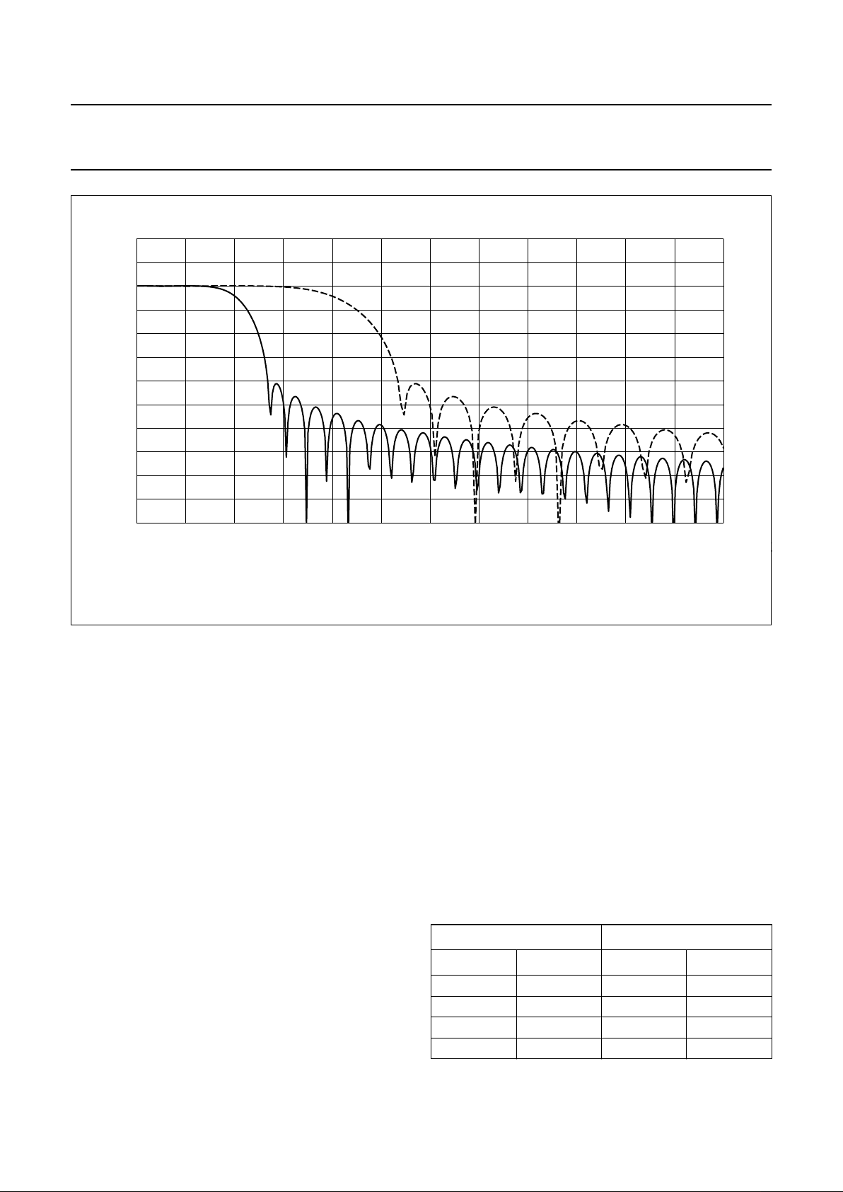
Fig.3 Transfer functions for the baseband receive filter.
3
handbook, full pagewidth
600500
f (kHz)
20
0
gain
(dB)
100 200 300 400
−20
−40
−60
−80
−100
0
MBL025
ZIF
NZIF
9.3 Baseband Serial Interface (BSI)
9.3.1 O
VERVIEW
The digital part of the baseband consists of a receive
section and a transmit section. The receive section is a
FIR filter that reduces the 6.5 MHz (13 MHz for
NZIF mode) bitstream from the sigma-delta converters
into 2 × 12-bit values at 270.833 kHz (541.667 kHz for
NZIF mode).
The transmit section converts the 270.833 kHz data
stream from the DSP into a GMSK signal sampled at
4.333 MHz. The 10-bit I and Q signals are then fed into
two 10-bit DACs. The power ramping signal is also
generated by the transmit section with the 10-bit
AUXDAC3 block.
9.3.2 T
RANSMIT PATH BLOCK DESCRIPTION
9.3.2.1 Transmit serial interface
The power-up of the BSI transmit path is controlled via the
TXON pin. When TXON is pulled HIGH, the transmit path
recovers from power-down. The MCLK/48 = 270.833 kHz
output signal BIOCLK is activated. When the BIEN0 period
has elapsed the output signal BIEN goes LOW and the bits
to be transmitted are clocked out of the DSP.
BIEN0 must be at least 10 quarterbits long to allow settling
of the analog filters. Bits are clocked out of the DSP by the
falling edge and clocked into the PCF50732 by the rising
edge of BIOCLK. After the BIEN1 period has elapsed,
BIEN is set HIGH again and transmission from the DSP
ends. Logic 1s are modulated whenever BIEN is HIGH
and the baseband transmit (BBTX) block is active. Values
for BIEN0 and BIEN1 can be set in the Burst control
register.
Figure 5 shows the timing for the BSI data transmission.
In power-down the de-asserted value of BIOCLK is high-Z
and BIEN is HIGH. Typical connection to the system DSP
is defined in Table 1.
Table 1 Connection of BSI transmit signals to
PCF5087X
PCF50732 PCF5087X
PIN I/O PIN I/O
TXON I RFSIG[y] O
BDIO I/O SIOXD I/O
BIEN O SOXEN_N I
BIOCLK O SIOXCLK I
Page 12

1999 May 03 12
Philips Semiconductors Objective specification
Baseband and audio interface for GSM PCF50732
9.3.2.2 Power ramping controller
The PCF50732 fully supports all multislot modes which do
not require full duplex operation or more than two
consecutive transmit bursts. In this specification double
burst mode is used for all supported multislot modes while
single burst mode supports the normal GSM modes.
The power ramping controller drives the power amplifier
output envelope.
In each transmit (TX) burst one ramp-up and one
ramp-down will be carried out. In multislot mode one
intermediate ramp will be carried out in addition to ramp-up
and ramp-down. Each ramp consists of 16 discrete step
values that are sent to the DAC3. Each step’s duration is
2 quarterbits which translates into 8-bit long ramps.
The DAC3 output is in 3-state whenever it is powered
down. The ramping step values are stored in a 64 × 10-bit
RAM as shown in Table 2.
In order to initialize AUXDAC3 it is necessary to write into
the RAM all 32 (or 48 in multislot mode) DAC3 output
values. Filling the RAM is normally done by writing a
logic 0 to the address sub-register of the Burst control
register, after which 32 or 48 values, depending on
multislot mode, can be written into the data sub-register of
the Burst control register. Writing to the DAC3 RAM is only
possible when the DAC3 is powered off.
Total number of CSI-accesses is therefore 33 for a normal
burst and 49 for a double burst.
An autoincrement feature will store these data into the
correct RAM positions.
The value after power-up of DAC3 will always be equal to
the value of RAM location 47.
AUXDAC3 timing is controlled by the Burst control
register. This contains the following sub-registers:
• The RU register containing the delay in number of
quarterbit cycles from the assertion of TXON to the start
of the power-up ramping; default value is 0
• The RM register containing the delay in number of
quarterbit cycles from the assertion of TXON to the start
of the intermediate power ramp; default value is 0. RM
is only used in case of multislot mode
• The RD register containing the delay in number of
quarterbit cycles from the assertion of TXON to the start
of the power-down ramping; default value is 0
• DAC3 burst RAM address register
• DAC3 burst RAM data register
• Single/double burst mode register: normal mode or
multislot mode selection flag.
After TXON goes HIGH and a time equal to RU quarterbit
periods has elapsed, power ramp-up is done.
After a time period equal to RD quarterbits has elapsed
power ramp-down is initiated.
The AUXDAC3 output is also shown in Fig.4.
Values for RU (ramp-up) and RD (ramp-down) can be set
in the Burst control register of the control serial interface.
RD must be greater than RU + 32. RU and RD range
from 0 to 4000 QB (quarterbit). The register offers the
possibility to enter codes up to 4095.
The GMSK modulator is active for a period of 2 clock
cycles after the ramp-down or for the length of the TXON
burst, whichever is longer.
Multislot (high speed switched data mode) can be selected
by setting the appropriate bit in the Burst control register.
In multislot mode an intermediate ramping step is done.
This intermediate step is started after a time period equal
to RM quarterbits has elapsed. A value for RM
(intermediate ramp) is also set using the Burst control
register. The following conditions must be true:
RU + 32 < RM and RM + 32 < RD.
Table 2 AUXDAC3 RAM contents
Table 3 Power ramping timing characteristics
Note
1. QB: Quarterbit, usually referred to the time needed for
one quarter of a GSM baseband bit, i.e. a frequency of
1
⁄12× 13 MHz.
RAM ADDRESS DATA
0 to 15 ramp-up data
16 to 31 intermediate ramp data
32 to 47 ramp-down data
48 to 64 not used
SYMBOL VALUE COMMENTS
(1)
t
0
12t
1
one quarterbit (QB)
t
ru
RU register 0 to 4000 QB
t
im
RM register RU + 32 to 4000 QB
t
rd
RD register RM + 32 to 4000 QB
t
rup
, t
rim
, t
rdo
32t
0
8 bits; 32 QB
Page 13
1999 May 03 13
Philips Semiconductors Objective specification
Baseband and audio interface for GSM PCF50732
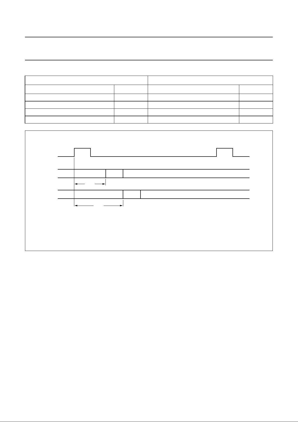
Fig.4 Power ramping timing characteristics (multislot mode).
(1) APE_DAC3: Analog Power Enable signal for the AUXDAC3.
andbook, full pagewidth
MGR995
t
rup
t
rim
t
rdo
RU RM RD
t
ru
AUXDAC3
TXON
APE_DAC3
(1)
ADDRESS
AUXDAC3
RAM
0
15 15 31
31 47154747
31
47
t
im
t
rd
9.3.3 RECEIVER PATH BLOCK DESCRIPTION
9.3.3.1 Receive serial interface
The baseband serial interface sends the digital signal of
the receive path to a digital signal processor. It also takes
the digital bitstream from the digital signal processor and
transmits it via the baseband CODEC.
The baseband reception and transmission are active in
bursts. A normal burst has a length of 548 µs. The frame
rate of bursts is 4.615 ms. Using a normal traffic channel,
one burst for each frame is transmitted and two bursts are
received. To save as much power as possible, the transmit
path and the receive path of the PCF50732 are in
power-up mode only during the transmission or reception
bursts respectively.
The power-up of the receive section is controlled via the
RXON pin or RXON bit. When RXON is driven HIGH, the
receive section recovers from power-down and the output
clock BIOCLK is activated. After a settling delay of 52 µs
(ZIF mode, analog circuitry + decimation filter settling
time), BOEN goes LOW to transfer the first 12-bit
I and Q words. The settling time is only 26 µs in NZIF
mode.
Bits are clocked out of the PCF50732 by the falling edge,
and clocked into the DSP by the rising edge of BIOCLK.
In normal bursts 148 I/Q pairs are read from the
PCF50732.
When RXON goes LOW, the last pair of I and Q values will
be sampled and transferred to the baseband processor
(both I and Q components). BIOCLK stops after additional
16 BIOCLK cycles. The receive path is powered down
again. In power-down the BIOCLK output is put in 3-state
and the BOEN output is HIGH.
The output format is 2 × 12-bit I/Q (twos complement).
Transmission occurs MSB first, I followed by Q. The serial
clock signal BIOCLK will run at 6.5 MHz, or 13 MHz in the
NZIF mode. Figure 6 shows the timing of the BSI data
reception.
An automatic offset compensation mechanism is provided
in order to achieve the required performance. This
mechanism will short the receive (RX) inputs internally and
measure the resulting offset value. This offset value will be
subtracted from all subsequent I/Q output words.
The offset inherent to the device can thereby be reduced
to a few millivolts. Default value for both I- and Q-offset is
zero.
Page 14

1999 May 03 14
Philips Semiconductors Objective specification
Baseband and audio interface for GSM PCF50732
Offset compensation measurement can be done on three
channels separately: baseband receive I channel,
baseband receive Q channel and AUXADC channel. All
AUXADC channels use the same offset compensation
value. Starting an offset measurement is done by writing a
logic 1 into the offset trigger register for each channel that
needs calibration. If the value ‘7’ (decimal) is written into
the offset trigger register offsets will be measured for I, Q
and AUXADC channels.
Offsets can also be read or written directly. Each offset
measurement is implemented internally as an AUXADC
measurement and takes approximately 100 µs.
Offsets from −256 up to 255 can be compensated.
Table 4 Connection of BSI receive signals to the
PCF5087X
PCF50732 PCF5087X
PIN I/O PIN I/O
RXON I RFSIG[z] O
BDIO I/O SIOXD I/O
BOEN O SIXEN_N I
BIOCLK O SIOXCLK I
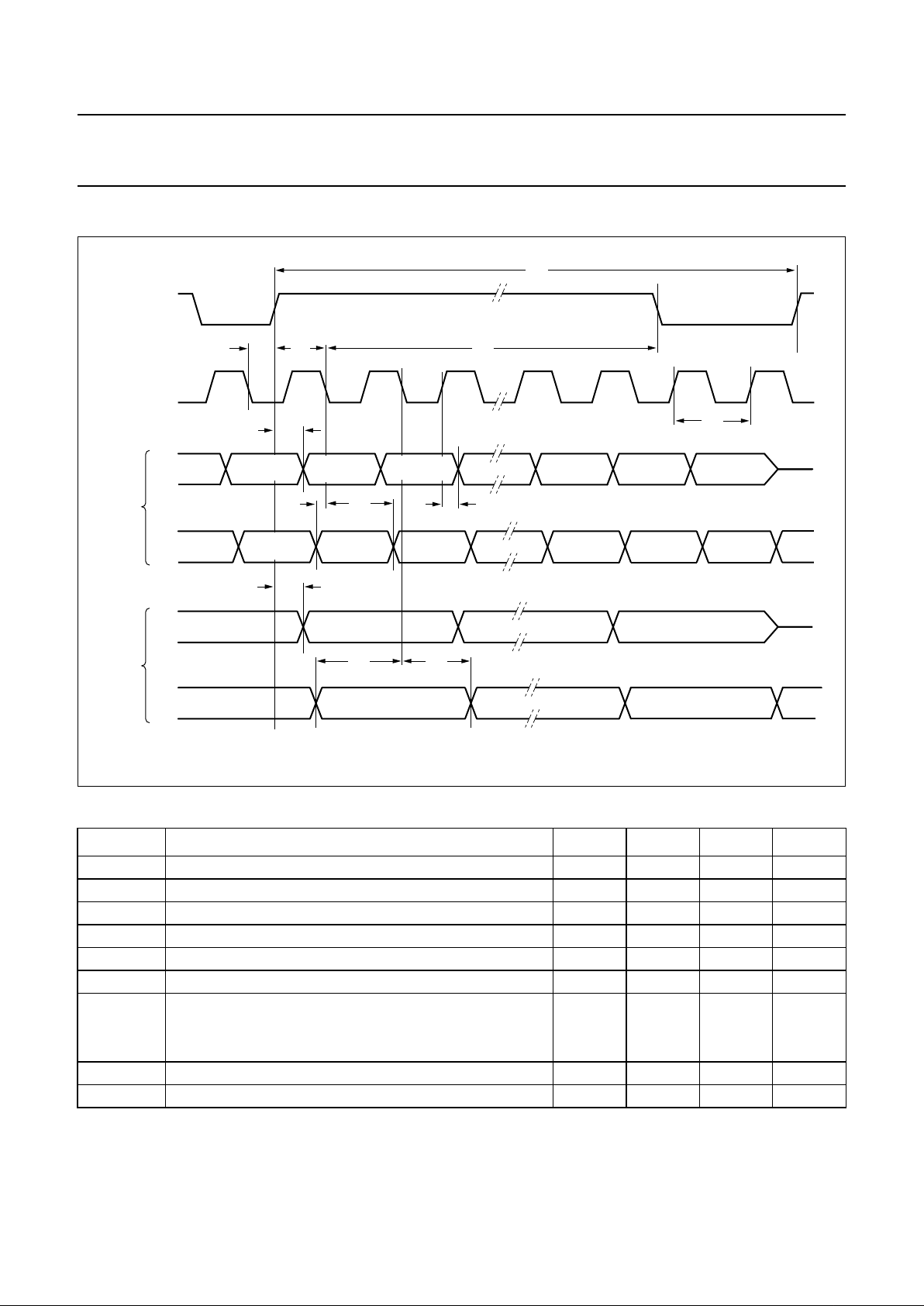
9.3.4 BASEBAND SERIAL INTERFACE (BSI) TIMING CHARACTERISTICS
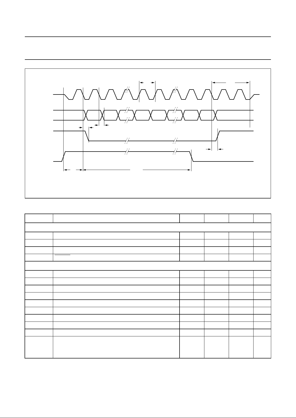
handbook, full pagewidth
MGR990
t
39
t
9
t
10
d.c.
(2)
logic 1s
logic 1s
data
data
data
data
d.c. d.c. B(0) B(n)B(1)
t
6
t
7
t
42
t
44
t
40
ramp-up
32 QB
intermediate ramp
32 QB
trail
2 BIOCLK
clocks
ramp-down
32 QB
t
43
high-Zhigh-Z
high-Zhigh-Z
BIOCLK
AUXDAC3
TXI/Q
(1)
BDIO
BIEN
TXON
t
5
Fig.5 Timing of the baseband serial interface transmit path; for the timing values see Table 5
(1) TXI/Q = transmit I or Q.
(2) d.c. = don’t care; will be overwritten with logic 1.
Page 15
1999 May 03 15
Philips Semiconductors Objective specification
Baseband and audio interface for GSM PCF50732
Table 5 BSI timing characteristics
SYMBOL PARAMETER MIN. TYP. MAX. UNIT
Master clock
t
1
MCLK cycle time − 76.9 − ns
t
2
MCLK LOW time 30
1
⁄2t
1
− ns
t
3
MCLK HIGH time 30
1
⁄2t
1
− ns
t
4
RESET LOW time 3t
1
−−ns
Baseband Serial Interface (BSI) transmit path (see Fig.5)
t
5
BIEN0 value 10 − 511 QB
t
6
BIEN1 value t
5
− 4000 QB
t
7
BIOCLK cycle time − 48t
1
− ns
t
9
data set-up time 20 −−ns
t
10
data hold time 20 −−ns
t
39
BIOCLK active after TXON rising edge −−t
1
ns
t
40
analog TX and GMSK power-up time −−17.4 QB
t
42
ramp-up value 0 − 3940 QB
t
43
intermediate ramp value 32 + t
42
− 3980 QB
t
44
ramp-down value
normal mode 32 + t
42
− 4020 QB
double burst mode 32 + t
43
− 4020 QB
Fig.6 Timing of the baseband serial interface receive path; for the timing values see Table 5.
handbook, full pagewidth
MGR991
t
14
t
13
I11 I0 Q11 Q0
t
15
t
11
548 µs
t
12
16t
1
high-Zhigh-Z
BIOCLK
BDIO
BOEN
RXON
Page 16

1999 May 03 16
Philips Semiconductors Objective specification
Baseband and audio interface for GSM PCF50732
Baseband Serial Interface (BSI) receive path (see Fig.6)
t
11
analog power-up and filter settling time
ZIF mode − 52 −µs
NZIF mode − 26 −µs
t
12
BIOCLK cycle time
ZIF mode − 2t
1
− ns
NZIF mode − t
1
− ns
t
13
BOEN LOW after falling clock edge −−15 ns
t
14
BIOCLK falling edge to data valid −−15 ns
t
15
BOEN HIGH after falling clock edge −−15 ns
SYMBOL PARAMETER MIN. TYP. MAX. UNIT
10 VOICE BAND CODEC
The voice band CODEC is a complete analog front-end
circuit. It consists of three parts:
• The receive path, which converts a digital linear PCM
signal to an analog signal for an earpiece, an external
loudspeaker or a buzzer
• The transmit path, which receives an analog signal
from a microphone or an auxiliary input and converts it
into a digital linear PCM signal
• The digital Audio Serial Interface (ASI), which
connects the digital linear PCM signals of the receive
and transmit paths to a digital signal processor.
Various functions and characteristics of the voice band
CODEC can be selected by programming the
corresponding control registers in the Control register
block (see also Tables 11, 22, 23, 24 and 25).
10.1 Voice band receive path
The voice band receive path consists of the following
parts:
• The receive part of the voice band signal processor
• NOISE SHAPER: 3rd order digital Σ∆ modulator,
generates a bit stream at 1 MHz to drive the EARDAC
• EARDAC: digital-to-analog converter including
low-pass filter for high frequency noise content of noise
shaper
• EARAMP: amplifier for an earpiece
• AUXAMP: amplifier for an auxiliary loudspeaker
• BUZAMP: amplifier for a buzzer output.
Linearity of receiver equipment (to earpiece) at
EARPGA = 0 dB and a volume control (VOLPGA and
EARAMP or AUXAMP) of−12 dB, signal-to-total harmonic
distortion ratio according to
“GSM recommendation
II.11.10 V.4.16.1”
.
10.1.1 RXVOL
RXVOL controls the volume of the voice band receive
path. In conjunction with EARAMP, AUXAMP and
BUZAMP it allows a gain variation from +6 to −30 dB in
64 steps; see Table 25. RXVOL also provides a mute
selection of the three outputs EARP/EARN, AUXSP and
BUZ respectively. At
RESET the volume is automatically
set to −12 dB.
10.1.2 RXPGA
RXPGA controls the gain of the voice band receive path
within a range of −24 to +12 dB in 64 steps for calibration
purposes.
10.1.3 RXFILTER
RXFILTER is a digital band-pass filter with a pass band
from 300 to 3400 Hz. It is realized by a programmable
structure (voice band signal processor).
10.1.4 EARDAC
EARDAC is a DAC operating at a sampling frequency of
1 MHz. It converts the bitstream input to a sampled
differential analog signal and low-pass filters the output
signal at the same time.
Page 17

1999 May 03 17
Philips Semiconductors Objective specification
Baseband and audio interface for GSM PCF50732
10.1.5 EARAMP
EARAMP is an amplifier, capable of driving a standard
earpiece with a minimum impedance of 8 Ω in
single-ended mode or 16 Ω in differential mode.
10.1.6 AUXAMP
AUXAMP is an amplifier for connection to an external
loudspeaker amplifier of minimum 8 Ω (hands-free car kit).
An‘auxiliary speaker external amplifier control’ output
pin (AMPCTRL) can be used to switch on/off an external
amplifier (hands-free car kit). The status of AMPCTRL is
programmable via the Control Serial Interface; its default
value is on.
10.1.7 BUZAMP
BUZAMP is an amplifier for connection to an external
buzzer of minimum 8 Ω. It has the same output
characteristics as the AUXAMP and can hence be used as
a second auxiliary output amplifier. It is switched on/off by
a dedicated control bit in the Control register block.
10.2 Voice band transmit path
The voice band transmit path consists of the following
parts:
• MICMUX: microphone input multiplexer
• MICADC: Σ∆ analog-to-digital converter
• DECIMATOR: decimates the incoming bit stream from
1 MHz to 40 kHz
• TXFILTER: band-pass filter for the digital transmit signal
and down-sampling
• TXPGA/LIM: fine-programmable gain for calibration,
limiter
• SidePGA: voice band sidetone programmable gain
amplifier.
Linearity of transmitter equipment, signal-to-total harmonic
distortion ratio according to
“GSM recommendation
II.11.10 V.4.16.1”
.
10.2.1 MICMUX
MICMUX is used to select between a differential signal at
pins MICP/MICN and a differential signal at pins
AUXMICP/AUXMICN.
Values are specified for a standard electret microphone
with a sensitivity of −64 ±3 dB for high gain or for an
external microphone with an amplifier sensitivity of
−26 ±3 dB (0 dB ≡ 1 V/0.1 Pa = 1 V/µbar; at 1 kHz).
10.2.2 MICADC
MICADC is a Σ∆ A/D converter which generates a 1 MHz
bitstream.
10.2.3 DECIMATOR
AND TXFILTER
The DECIMATOR is a digital filter, which performs a signal
processing to a lower sampling rate at the output
compared to the input.
The bitstream with a sampling frequency of 1 MHz is
low-pass filtered and down-sampled to 40 kHz by a FIR
filter.
A digital high-pass filter and a digital low-pass filter (both
IIR filters) process the 14-bit input samples to achieve a
band-pass with a pass band from 300 to 3400 Hz. These
filters run on the on-chip voice band signal processor (see
Fig.7). It’s program is down-loaded into the instruction
memory (IRAM) via the CSI (see Table 26).
The output of the TXFILTER is down-sampled to a
sampling frequency of 8 kHz with a word length of 16 bits.
10.2.4 TXPGA
TXPGA adapts the analog signals coming from MICMUX
within a range of−30 to +6 dB. It is designed for calibration
purposes.
10.2.5 SIDEPGA
SidePGA loops part of the voice band transmit signal back
into the receive path. There are 64 gain steps from mute to
+6 dB.
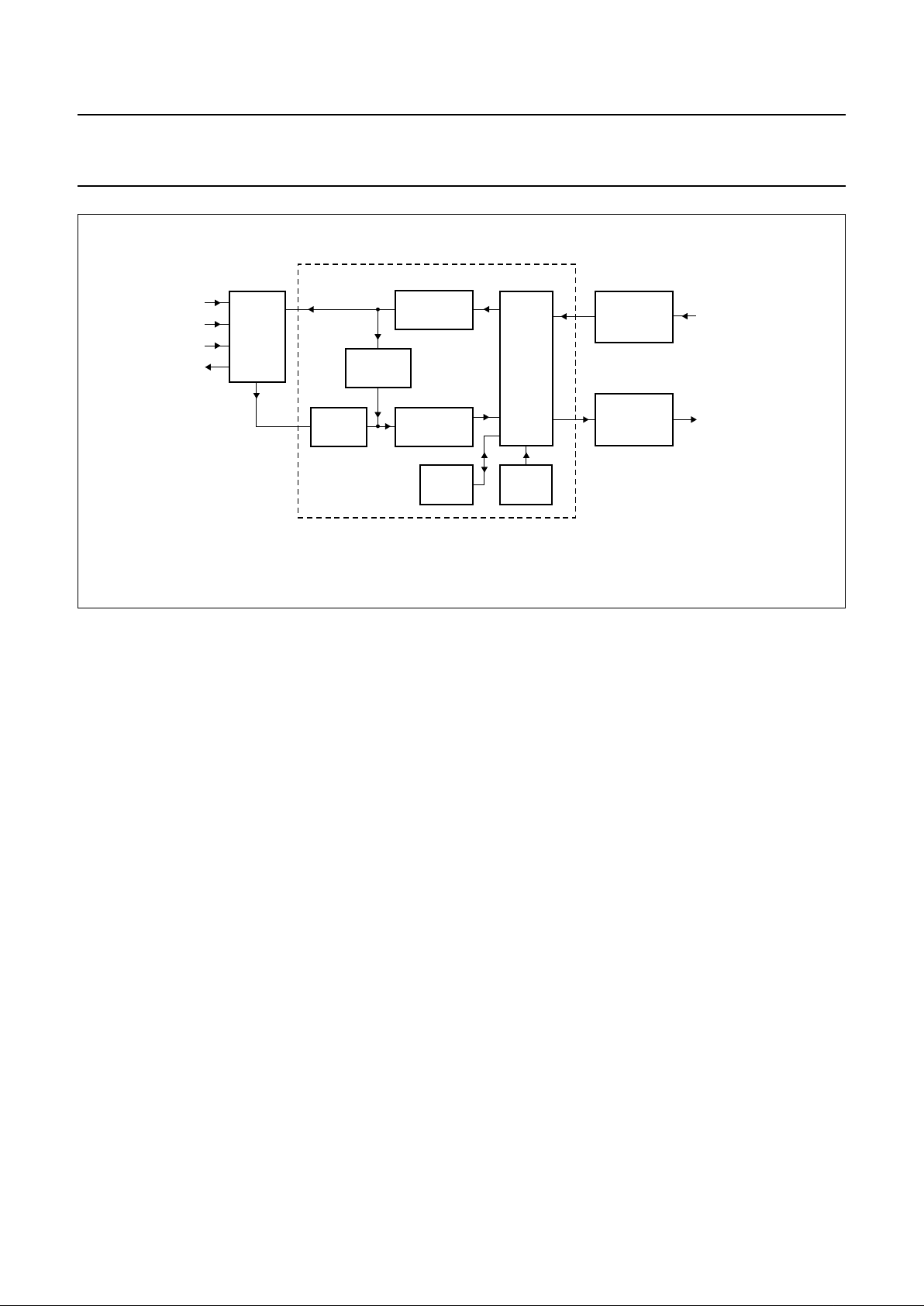
10.3 Voice band digital circuitry
The voice band digital circuitry is responsible for
converting a 16-bit PCM signal at 8 kHz sample rate to and
from a 1-bit 1 MHz signal. It also contains a band-pass
filter for 300 to 3400 Hz and a sidetone engine. Various
volume settings are calculated inside this block. Figure 7
shows the block diagram of the voice band signal
processor.
Page 18
1999 May 03 18
Philips Semiconductors Objective specification
Baseband and audio interface for GSM PCF50732
Fig.7 Block diagram of the voice band signal processor.
handbook, full pagewidth
MGR992
DECIMATOR
16-bit, 8 kHz
1-bit, 1 MHz
ASI
ADI
ACLK
AFS
ADO
RX_BS
(receive bitstream)
TX_BS
(transmit bitstream)
RX/TX
FILTER
VOICE BAND SIGNAL PROCESSOR
TXPGA/LIM
RXPGA/LIM
RXVOL
SidePGA
RRAM IRAM
NOISE
SHAPER
10.3.1 VOLUME CONTROL BLOCK
The volume control block contains the RXPGA, SidePGA,
TXPGA and both limiter blocks. The possible settings can
be found in the description of the CSI block. All digital
volume control blocks, i.e. RXPGA, SidePGA, and
TXPGA, will allow settings from +6 to −30 dB and mute in
64 steps. However, not all combinations of settings for
these blocks will be meaningful. The limiter will always clip
signals with overflow to the maximum or minimum
allowable value.
10.3.2 A
UDIO SERIAL INTERFACE (ASI) BLOCK
The ASI is the voice band serial interface which provides
the connection for the exchange of PCM data in both
receive and transmit directions, between the baseband
digital signal processor and the PCF50732. The data is
coded in 16-bit linear PCM twos complement words.
A frame start is defined by the first falling edge of ACLK
after a rising AFS. This first falling edge is used to clock in
the first data bit on both the baseband and the DSP device.
Data on pin ADI is clocked in (MSB first) on the falling edge
of the ACLK clock. Data is clocked out (MSB first) on pin
ADO on the rising edge of the ACLK clock.
Pin ADO is put in 3-state after the LSB of the transmit
word, independent of the length of the AFS pulse. If the
channel position 0 (see Section 10.3.2.1) is selected, then
the MSB must be output directly after AFS becomes a
logic 1, even if no rising edge on ACLK has been given yet.
The following modes of operation are programmable:
channel position and ACLK clock mode.
10.3.2.1 Channel position mode
Depending on a programmable register value n
(n = 0 to 15) one of 16 channels can be selected (see
Table 22). The ASI can add a delay of 16 × n-bit clocks
between the assertion of AFS and the start of the MSB of
the PCM values. This delay is independently
programmable for transmit and receive mode.
10.3.2.2 ACLK clock mode
Single or double clock mode can be selected. Double clock
mode implies two clock pulses per data bit and is used for
communication with IOM2 compatible devices. In double
clock mode data must be output on the first rising edge and
be read on the last falling edge.
Page 19
1999 May 03 19
Philips Semiconductors Objective specification
Baseband and audio interface for GSM PCF50732
Table 6 Pin connection of the audio serial interface to the PCF5087X
PCF50732 PCF5087X
PIN I/O PIN I/O
ADI I DD O
ADO O DU I
ACLK I DCL O
AFS I FSC O
Fig.8 Frame structure of the Audio Serial Interface (ASI).
t
rpdc
: receive path data channel delay.
t
tpdc
: transmit path data channel delay.
handbook, full pagewidth
MGR993
word
word
AFS
ADI
ADO
t
tpdc
t
rpdc
Page 20
1999 May 03 20
Philips Semiconductors Objective specification
Baseband and audio interface for GSM PCF50732
10.3.2.3 Audio Serial Interface (ASI) timing characteristics
Table 7 ASI timing characteristics
SYMBOL PARAMETER MIN. TYP. MAX. UNIT
t
16
frame sync (AFS) set-up time to falling edge of ACLK 70 −−ns
t
17
frame sync (AFS) hold time from falling edge of ACLK 40 −−ns
t
18
ACLK rising edge to data (ADO) valid −30 − +30 ns
t
19
data (ADI) set-up time to falling edge of ACLK 50 −−ns
t
20
data (ADI) hold time from falling edge of ACLK 80 −−ns
t
21
first data valid (ADO) after AFS rising edge 0 − 60 ns
t
40
ACLK period
single clock mode 0.5 − 7.8 µs
double clock mode 0.5 − 3.9 µs
t
41
AFS period − 125 −µs
t
42
ACLK LOW before AFS rising edge 40 −−ns
Fig.9 Timing of the Audio Serial Interface (ASI).
handbook, full pagewidth
MGR994
single
clock
mode
ADO
ACLK
AFS
ADI
t
41
last slot
last bit
last slot
last bit
first slot
first bit
MSB
LSB
first slot
second bit
last slot
last bit
last slot
last bit
first slot
first bit
MSB LSB
first slot
second bit
double
clock
mode
ADO
ADI
last slot
last bit
last slot
last bit
first slot
first bit
MSB LSB
high-Z
high-Z
slot 1
bit 2
last slot
last bit
last slot
last bit
first slot
first bit
MSB
LSB
slot 1
bit 2
t
16
t
42
t
17
t
40
t
21
t
20
t
18
t
19
t
19
t
20
t
21
Page 21

1999 May 03 21
Philips Semiconductors Objective specification
Baseband and audio interface for GSM PCF50732
11 AUXILIARY FUNCTIONS
The auxiliary functions part consists of three
digital-to-analog converters (DACs) and a 4 input
analog-to-digital converter (ADC) with a 12-bit range.
The DACs are for:
• Automatic Gain Control (AGC): AUXDAC1
• Automatic Frequency Control (AFC): AUXDAC2
• Power ramping: AUXDAC3.
11.1 Automatic Gain Control (AGC): AUXDAC1
The AUXDAC1 is an 8-bit binary coded, guaranteed
monotonic digital-to-analog converter.
The status of AUXDAC1 is controlled by the signal AUXST
and a power-up bit in the Power control register. The signal
that switches the external VCXO can also be used to
control the AUXST pin of the PCF50732. The AUXDAC1
output is floating in Power-down mode (AUXST = LOW).
The input MCLK is then deactivated.
When AUXST goes HIGH, AUXDAC1 is powered-up and
the converted value of the corresponding register in the
control register block is available at the AUXDAC1 output
pin.
If a write access to the AUXDAC1 register occurs, the DAC
is activated with the new content of the DAC register (see
Table 14 and 15). The AUXDAC1 must be powered-up by
setting the correct bit in the Power control register. At reset
AUXDAC1 is powered-down.
11.2 Automatic Frequency Control (AFC):
AUXDAC2
The AUXDAC2 is a 12-bit binary coded, guaranteed
monotonic digital-to-analog converter. This DAC is used to
control the frequency of an external master clock VCXO.
The status of AUXDAC2 is controlled by the signal AUXST
and a power-up bit in the Power control register. The signal
that switches the external VCXO can also be used to
control the AUXST pin of the PCF50732. The AUXDAC2
output is floating in Power-down mode (AUXST = LOW).
When AUXST goes HIGH, AUXDAC2 is powered-up and
the converted value of the corresponding register in the
control register block is available at the AUXDAC2 output
pin.
The default value for AUXDAC2 is 1.1 V which
corresponds to a 800H code in the AUXDAC2 register.
At reset AUXDAC2 is powered on.
11.3 Power ramping: AUXDAC3
AUXDAC3 is a 10-bit binary coded digital-to-analog
converter designed for power ramping purposes.
AUXDAC3 is default off. The power ramping behaviour is
described in Section 9.3.2.2.
11.4 Auxiliary analog-to-digital converter (AUXADC)
The AUXADC is specified for voltage and temperature
measurements. It contains 4 input channels required for
∆T and ∆V measurements, as well as battery type
recognition:
•∆T: battery temperature, ambient temperature
(measured across sensor)
•∆V: peak battery voltage, battery voltage during transmit
burst.
Five 12-bit registers are available in which results of
auxiliary analog-to-digital conversions can be stored.
Two registers are dedicated to the input AUXADC1 and
one to each of AUXADC2, AUXADC3 and AUXADC4.
The AUXADC1 input can be used for battery voltage
measurement. In the AUXADC1A register the voltage
during a transmit time slot can be stored. The AUXADC1B
register can store the voltage during other time slots. If a
read request to one of these registers is executed by
loading its address into the Read request register, the
actual contents of the addressed register are given to the
control interface and a new measurement is performed in
the next appropriate time slot.
A multiplexer connects each of the AUXADC inputs to a
channel of the receive ADC depending on read access to
the corresponding register.
Thus an auxiliary analog-to-digital conversion is only
possible, if the baseband receive section is not in use
(RXON is LOW). At each read request to one of the
AUXADC registers, a flag is set in the AUXADC flag
register indicating that an analog-to-digital conversion is to
be performed. When one of the registers AUXADC1B,
AUXADC2, AUXADC3, or AUXADC4 is being read, the
baseband interface verifies that RXON is LOW, indicating
that no receive burst is currently active. The baseband
receive path is then powered up. After the ADC settling
time has elapsed (see POST
AUXADC
in Chapter 18), valid
data is available and stored in the corresponding register.
Page 22

1999 May 03 22
Philips Semiconductors Objective specification
Baseband and audio interface for GSM PCF50732
After conversion the corresponding bit in the AUXADC flag
register is reset (see Table 18). If RXON is activated
during an auxiliary analog-to-digital conversion cycle, the
auxiliary conversion is interrupted and restarted when
RXON returns LOW, indicating no receive burst activity.
When register AUXADC1A is read, a battery voltage
measurement during a transmission burst is executed.
The PCF50732 waits for a rising edge of TXON, and
powers up the receive path. After the settling time of the
ADC added to the programmed AUXADC conversion
delay (in 48 MCLK cycles) has elapsed, valid data is
available and stored in the AUXADC1A register.
Fig.10 Typical transfer characteristics of AUXADC (output code as function of differential input voltage).
handbook, full pagewidth
MGR996
0
1440
0.2
output code
(LSB)
offset
at 0 V
gain tolerance
0 0.4 0.6 0.8 1.0 1.2 1.4 1.6 1.8 2.0
Vin (V)
Page 23

1999 May 03 23
Philips Semiconductors Objective specification
Baseband and audio interface for GSM PCF50732
12 CONTROL SERIAL INTERFACE (CSI)
The Control Serial Interface block is used to set and read
the status bits inside the PCF50732. It is also used to read
data from the auxiliary ADCs and to write data into the
auxiliary DACs. Finally, the block is used to write the power
ramping curve into a 64 × 10-bit static RAM. It should be
noted that only 48 of the 64 addresses can be accessed;
see Table 2.
12.1 The serial interface
A 4-line bidirectional serial interface is used to control the
circuit. It allows access to each register of the control
register block (read and/or write). The 4 lines are:
• Data in (CDI)
• Data out (CDO)
• Clock (CCLK)
• Enable (CEN).
Table 8 lists the normal connections to the PCF5087X.
The data sent to or from the device is loaded in bursts
framed by CEN. Clock edges and data bits are ignored
until CEN goes active (LOW). Each data word consists of
21 bits that comprises a 4-bit device address, a 4-bit
register address, a 12-bit data word and a dummy bit; see
Table 9. The 21 bits are transmitted with MSB first.
Figure 5 shows the valid timing for data transmission on
the control interface.
Data is read in from the CDI pin on the rising edge of the
CCLK clock and output on CDO on the falling edge of the
CCLK clock. Data is written into the registers on the rising
edge of CEN.
If the device address is equal to the chip address, the
programmed information on CDI (DB11 to DB00) is loaded
into the addressed register (RA3 to RA0) when CEN
returns inactive HIGH.
The dummy bit in front is needed for compatibility with
older baseband devices.
Reading a register is accomplished by writing the address
of the required register into the read request register.
The next time CEN goes LOW, the requested data will be
shifted out, together with the register and device address.
Table 8 Pin connection of the CSI to the PCF5087X
Table 9 Bit mapping of the 21-bit words
PCF50732 PCF5087X
PIN I/O PIN I/O
CDI I RFDO O
CDO O RFDI I
CCLK I RFCLK O
CEN I RFE_N2 O
BIT CONTENT DESCRIPTION
00 to 03 ADD0 to ADD3 device address; for the
PCF50732 this is ‘1001’
(= 9 decimal)
04 to 07 RA0 to RA3 register address
08 to 19 DB00 to DB11 data value
20 dummy don’t care
Page 24

1999 May 03 24
Philips Semiconductors Objective specification
Baseband and audio interface for GSM PCF50732
12.2 Control Serial Interface (CSI) timing characteristics
Table 10 CSI timing characteristics
For the timing diagram see Fig.11.
SYMBOL PARAMETER MIN. MAX. UNIT
t
22
CEN set-up time 20 − ns
t
23
CDO data valid after falling clock edge − 50 ns
t
24
CCLK cycle time 100 − ns
t
25
data set-up time to rising edge of CCLK 20 − ns
t
26
data hold time from rising edge of CCLK 30 − ns
t
27
CEN hold time 30 − ns
t
37
CDO 3-state after CEN HIGH − 30 ns
t
38
CEN HIGH time 50 − ns
Fig.11 Timing diagram of the Control Serial Interface (CSI).
handbook, full pagewidth
MGR997
CDI
CEN
CCLK
CDO
ADD0(#0)MSB(#19)dummy
t
27
t
38
t
22
t
23
t
23
t
24
t
37
ADD0(#0)MSB(#19)
dummy
high-Z
t
25t26
Page 25

1999 May 03 25
Philips Semiconductors Objective specification
Baseband and audio interface for GSM PCF50732
12.3 Control register block
This section describes the different registers that are implemented in the PCF50732. An overview is given in Table 11.
Tables 12 to 29 describe all the registers of the PCF50732.
Table 11 Control register block overview
Notes
1. See description in Section 11.4.
2. Do not use this register.
12.3.1 READ REQUEST REGISTER
Table 12 Read request register
X = don’t care during a read/or write access.
Table 13 Read request registers value description
ADDRESS ACCESS REGISTER NAME
0000 W Read request register
0001 R/W AUXDAC1 (AGC) value register
0010 R/W AUXDAC2 (AFC) value register
0011 R/W Burst control register
0100 R/W AUXADC control register
0101 R AUXADC channel 1 register A (AUXADC1A); note 1
0110 R AUXADC channel 1 register B (AUXADC1B); note 1
0111 R AUXADC channel 2 register (AUXADC2); note 1
1000 R AUXADC channel 3 register (AUXADC3); note 1
1001 R AUXADC channel 4 register (AUXADC4); note 1
1010 R/W Voice band control register
1011 R/W Voice band volume register
1100 R/W Power control register
1101 R/W RAM interface register
1110 R/W Baseband receive control register
1111 R/W Test mode register; note 2
ADDRESS REGISTER NAME
VALUE
11109876543210
0000 Read request register X X X X r3 r2 r1 r0 s3 s2 s1 s0
VALUE OF SYMBOL DESCRIPTION
Read request register r3 to r0 Address of the register to be read.
s3 to s0 Subaddress that might be needed. The subaddress bits are right
aligned, meaning that the subaddress always starts with bit ‘s0’ (LSB);
e.g. in case of two subaddress bits, ‘s1’ and ‘s0’ are used.
Page 26

1999 May 03 26
Philips Semiconductors Objective specification
Baseband and audio interface for GSM PCF50732
12.3.2 AUXDAC1 (AGC) VALUE AND AUXDAC2 (AFC) VALUE REGISTERS
Table 14 Registers overview
X = don’t care during a read/or write access.
Table 15 AUXDAC1 (AGC) value and AUXDAC2 (AFC) value registers value description
12.3.3 BURST CONTROL REGISTER
The Burst control register controls the timing of the transmit burst (TX-burst). The ‘lo’-registers contain the lower 8 bits,
the ‘hi’-registers the upper 4 bits of a 12-bit delay value. Therefore, each register has a programmable range
from 0 to 4095. Not all combinations of values might make sense e.g. ramp-down before ramp-up.
Table 16 Burst control register (address 001 and subaddresses)
X = don’t care during a read/or write access.
Notes
1. The programming is described in Section 9.3.2.2.
2. The subaddress positions bit 9 (s1) and bit 8 (s0) do not apply to the DAC3 burst RAM data register.
ADDR. REGISTER NAME
VALUE
11109876543210
0001 AUXDAC1 (AGC) value register X X X X b7 b6 b5 b4 b3 b2 b1 b0
0010 AUXDAC2 (AFC) value register b11 b10 b9 b8 b7 b6 b5 b4 b3 b2 b1 b0
VALUE OF SYMBOL DESCRIPTION
AUXDAC1 (AGC) value register b7 to b0 input value to the 8-bit AUXDAC1 (fed directly into the DAC); the default
value is 85H
AUXDAC2 (AFC) value register b11 to b0 input value to the 8-bit AUXDAC2 (fed directly into the DAC); the default
value is 800H
FUNCTION
SUBADDRESS VALUE
11
(s3)10(s2)9(s1)8(s0)
76543210
RU-lo 0 0 0 0 b7 b6 b5 b4 b3 b2 b1 b0
RU-hi 0 0 0 1 X X X X b11 b10 b9 b8
RM-lo 0 0 1 0 b7 b6 b5 b4 b3 b2 b1 b0
RM-hi 0 0 1 1 X X X X b11 b10 b9 b8
RD-lo 0 1 0 0 b7 b6 b5 b4 b3 b2 b1 b0
RD-hi 0 1 0 1 X X X X b11 b10 b9 b8
BIEN0-lo 0 1 1 0 b7 b6 b5 b4 b3 b2 b1 b0
BIEN0-hi 0 1 1 1 X X X X b11 b10 b9 b8
BIEN1-lo 1 0 0 0 b7 b6 b5 b4 b3 b2 b1 b0
BIEN1-hi 1 0 0 1 X X X X b11 b10 b9 b8
Single/double burst mode
(1)
1 0 1 0XXXXXXXb0
DAC3 burst RAM address
(1)
1 0 1 1 X X a5 a4 a3 a2 a1 a0
DAC3 burst RAM data
(1)
11d9
(2)
d8
(2)
d7 d6 d5 d4 d3 d2 d1 d0
Page 27

1999 May 03 27
Philips Semiconductors Objective specification
Baseband and audio interface for GSM PCF50732
Table 17 Burst control registers value description
12.3.4 AUXADC CONTROL REGISTER
Table 18 AUXADC control register (address 0100 and subaddresses)
X = don’t care during a read/or write access.
VALUE OF DESCRIPTION
RU Value RU, consisting of RU-lo (least significant byte) and RU-hi (most significant byte), is the delay
measured in quarterbits (
1
⁄12MCLK) between the rising edge of TXON and the start of the ramp-up on
AUXDAC3. After this delay , the first 16 values of the AUXDAC3 RAM are sent to AUXDAC3. Shifting out
is done at1⁄24MCLK.
RM Value RM, consisting of RM-lo (least significant byte) and RM-hi (most significant byte), is the delay
measured in quarterbits between the rising edge of TXON and the start of the intermediate ramp in a
double burst ramp. The RM value is only used in multislot mode. RM must be greater than RU + 32.
RD Value RD, consisting of RD-lo (least significant byte) and RD-hi (most significant byte), is the delay
measured in quarterbits between the rising edge of TXON and the start of the ramp-down on AUXDAC3.
RD must be greater than RU + 32, or in case of multislot mode, greater than RM + 32.
BIEN0 Value BIEN0, consisting of BIEN0-lo (least significant byte) and BIEN0-hi (most significant byte), is the
delay measured in quarterbits between the rising edge of TXON and the falling edge of BIEN.
BIEN1 Value BIEN1, consisting of BIEN1-lo (least significant byte) and BIEN1-hi (most significant byte), is the
delay measured in quarterbits between the rising edge of TXON and the rising edge of BIEN. BIEN1
must be greater than BIEN0.
FUNCTION
SUBADDRESS VALUE
11
(s2)10(s1)9(s0)
8765432 1 0
AUXADC conversion delay
value register
000XXb6b5b4b3b2 b1 b0
AUXADC flag register 0 0 1 X Qoff Ioff auxoff flag 4 flag 3 flag 2 flag 1B flag 1A
AUXADC offset value
register
1 0 0 9-bit signed offset compensation value
I channel offset value
register
1 0 1 9-bit signed offset compensation value
Q channel offset value
register
1 1 0 9-bit signed offset compensation value
Offset trigger register 1 1 1 X X X X X X Q-off I-off Aux
Page 28

1999 May 03 28
Philips Semiconductors Objective specification
Baseband and audio interface for GSM PCF50732
Table 19 AUXADC control registers value description
12.3.5 AUXADC REGISTERS
Table 20 AUXADC registers overview
Table 21 AUXADC registers value description
VALUE OF DESCRIPTION
AUXADC conversion delay
value register
The 7-bit value (b6 to b0) denotes the delay measured in 48MCLK units between the
rising edge of TXON and the conversion on AUXADC1A. The normal power-on
settling time is added to this delay. Default value is 0.
AUXADC flag register The AUXADC flag register returns the status of the AUXADC converters. If an
auxiliary A/D conversion is pending, the flag of the corresponding AUXADC will be
set. The flag register is read only.
AUXADC offset value register The offset value registers contain signed 9-bit offset compensation values. These
values are subtracted automatically from all baseband receive (BBRX) and AUXADC
measurements to compensate for offset errors. The compensation values can be
read and written and have a default value of 0. It can also be measured by the device
itself.
A write to the Offset trigger register will trigger an offset measurement for each of the
channels (Q-off, I-off or AUXADC) selected.
Offset measurements are special cases of AUXADC measurements and are done
sequentially. Each calibration measurement takes approximately 100 µs. The Offset
trigger register is write only.
I channel offset value register
Q channel offset value register
Offset trigger register
ADDR. REGISTER NAME
VALUE
11109876543210
0101 AUXADC channel 1 register A (AUXADC1A)
b11 b10 b9 b8 b7 b6 b5 b4 b3 b2 b1 b0
0110 AUXADC channel 1 register B (AUXADC1B)
0111 AUXADC channel 2 register (AUXADC2)
1000 AUXADC channel 3 register (AUXADC3)
1001 AUXADC channel 4 register (AUXADC4)
VALUE OF DESCRIPTION
AUXADC1A 12-bit result of the A/D conversion on AUXADC channel 1, measured during a transmission burst
AUXADC1B 12-bit result of the A/D conversion on AUXADC channel 1, measured outside a transmission burst
AUXADC2 12-bit result of the A/D conversion on AUXADC channel 2
AUXADC3 12-bit result of the A/D conversion on AUXADC channel 3
AUXADC4 12-bit result of the A/D conversion on AUXADC channel 4
Page 29

1999 May 03 29
Philips Semiconductors Objective specification
Baseband and audio interface for GSM PCF50732
12.3.6 VOICE BAND CONTROL REGISTER
The Voice band control register is used to control the following functionality of the voice band CODEC:
• Analog input source: microphone (MICAMP) or auxiliary (AUXMIC) input
• Analog output device: earphone (EARAMP), auxiliary (AUXAMP) or buzzer (BUZAMP) output; this register allows
individual control of all three output amplifiers
• EARAMP output mode: single-ended (EARP) or differential (EARN/EARP). This selects the input source for the
EARAMP-N amplifier. In single-ended mode EARAMP-N will be at V
ref
, in differential mode it will carry the output signal
• General purpose output pin: AMPCTRL
• Receive and transmit path delay values
• ASI clock mode
• TX gain boost (MICHI).
Table 22 Voice band control register (address 1010 and subaddresses)
X = don’t care during a read/or write access.
FUNCTION
SUBADDRESS VALUE
FUNCTION SETTING
11
(s2)10(s1)9(s0)
876543210
Select input source 0 0 0 don’t care
0 MICAMP (default)
1 AUXMIC
Select output amplifier 0 0 1 don’t care
X X X 0 EARAMP-P off
X X X 1 EARAMP-P on (default)
X X 0 X EARAMP-N off
X X 1 X EARAMP-N on (default)
X 0 X X AUXAMP off (default)
X 1 X X AUXAMP on
0 X X X BUZAMP off (default)
1 X X X BUZAMP on
EARAMP output mode 0 1 0 don’t care
0 single-ended
1 differential (default)
AMPCTRL pin polarity 0 1 1 don’t care
0 active LOW
1 active HIGH (default)
Receive path data channel 1 0 0
don’t care
dcba
4-bit delay value (default = 0)
Transmit path data channel 1 0 1 d c b a
ASI clock mode 1 1 0 don’t care
0 single clock (default)
1 double clock
TX gain boost (MICHI) 1 1 1 don’t care
07dB
1 35 dB (default)
Page 30

1999 May 03 30
Philips Semiconductors Objective specification
Baseband and audio interface for GSM PCF50732
12.3.7 VOICE BAND VOLUME REGISTER
Voice band gain settings can be independently programmed for: TXPGA, RXPGA, RXVOL and SidePGA.
Table 23 Voice band volume register (address 1011 and subaddresses)
X = don’t care during a read/or write access.
Table 24 Voice band volume registers value description
Note
1. Possible gain settings are listed in Table 25 or can be calculated using the following formulae (‘n’ is an integer that
represents the value that is written into the register; n = 0 to 63):
a) RXPGA and TXPGA: ; add 6.02 dB to each gain for RXPGA and TXPGA settings.
b) RXVOL and SidePGA:
FUNCTION
SUBADDRESS VALUE
SELECTED
RANGE
DEFAULT
SETTING
11
(s2)10(s1)9(s0)
8765 4 3 2 1 0
TXPGA gain 0 0 0 X X X a b c d e f
−24 to +12 dB 0 dB
RXPGA gain 0 0 1 X X X a b c d e f
RXVOL gain 0 1 0 X X X a b c d e f
−30 to +6 dB
−12 dB
SidePGA gain 0 1 1 X X X a b c d e f mute
Band gap setting level 1 0 0 X X X a b c X X X −100 to +75 mV 0 mV offset
Experimental bits 1 0 1 X X X dir pll dc vbch hclk bgb − pll on, all
others off
VALUE REMARKS DESCRIPTION
TXPGA gain microphone calibration
TXPGA and RXPGA settings use the 6-bit binary fixed point value
‘ab.cdef’ as a multiplier for each PCM-sample. This results in a
control range of +12 to −24 dB. See note 1a.
RXPGA gain earphone calibration
RXVOL gain customer volume control
RXVOL and SidePGA settings use the 6-bit binary fixed point
value ‘a.bcdef’ as a multiplier for each PCM-sample. This results
in a control range of +6 to −30 dB (and mute). See note 1b.
SidePGA gain −
Experimental bits −•dir: bypass clock buffer
• pll: clock optimizer
• dc: bypass clock capacitor
• vbch: voice band chopping
• hclk: 26 MHz master clock input
• bgb: band gap boost
Band gap setting level do not use
gain 20
n
16
------log×=
gain 20
n
32
------log×=
Page 31

1999 May 03 31
Philips Semiconductors Objective specification
Baseband and audio interface for GSM PCF50732
12.3.7.1 Possible gain selections for voice band blocks: RXPGA, TXPGA, RXVOL and SidePGA
Table 25 shows the possible gain selections for the voice band blocks RXPGA, TXPG, RXVOL and SidePGA. It should
be noted that not all possible combinations of these volume settings are meaningful; setting RXPGA, SidePGA and
RXVOL to maximum will result in clipping of the output signal.
Table 25 Gain selections
BINARY
CODE
GAIN (dB)
RXPGA/TXPGA RXVOL/SidePGA
111111 11.88 5.88
111110 11.74 5.74
111101 11.60 5.60
111100 11.46 5.46
111011 11.31 5.31
111010 11.17 5.17
111001 11.01 5.01
111000 10.86 4.86
110111 10.70 4.70
110110 10.54 4.54
110101 10.38 4.38
110100 10.22 4.22
110011 10.05 4.05
110010 9.88 3.88
110001 9.70 3.70
110000 9.52 3.52
101111 9.34 3.34
101110 9.15 3.15
101101 8.96 2.96
101100 8.77 2.77
101011 8.57 2.57
101010 8.36 2.36
101001 8.15 2.15
101000 7.94 1.94
100111 7.72 1.72
100110 7.49 1.49
100101 7.26 1.26
100100 7.02 1.02
100011 6.78 0.78
100010 6.53 0.53
100001 6.27 0.27
100000 6.00 0.00
011111 5.72 −0.28
011110 5.44 −0.56
011101 5.14 −0.86
011100 4.84 −1.16
011011 4.52 −1.48
011010 4.20 −1.80
011001 3.86 −2.14
011000 3.50 −2.50
010111 3.13 −2.87
010110 2.75 −3.25
010101 2.34 −3.66
010100 1.92 −4.08
010011 1.47 −4.53
010010 1.00 −5.00
010001 0.51 −5.49
010000 0.00 −6.02
001111 −0.58 −6.58
001110 −1.18 −7.18
001101 −1.82 −7.82
001100 −2.52 −8.52
001011 −3.28 −9.28
001010 −4.10 −10.10
001001 −5.02 −11.02
001000 −6.04 −12.04
000111 −7.20 −13.20
000110 −8.54 −14.54
000101 −10.12 −16.12
000100 −12.06 −18.06
000011 −14.56 −20.56
000010 −18.08 −24.08
000001 −24.10 −30.10
000000 off off
BINARY
CODE
GAIN (dB)
RXPGA/TXPGA RXVOL/SidePGA
Page 32

1999 May 03 32
Philips Semiconductors Objective specification
Baseband and audio interface for GSM PCF50732
12.3.8 POWER CONTROL REGISTER
The Power control register is used to control power-up and power-down of the different sections of the device. Changing
the power status is accomplished by addressing the device as shown in Table 26 and setting bit 0 (= a) according to the
required state:
a=0→power-down
a=1→power-up.
Setting the baseband RX or TX flag is functionally equivalent to setting RXON or TXON respectively (logical
OR function). The CSI is also accessible when the band gap is powered down. Therefore no reset is required to power-up
after total power-down.
Table 26 Power control register (address 1100 and subaddresses)
FUNCTION
SUBADDRESS VALUE DEFAULT
11
(s3)10(s2)9(s1)8(s0)
7 6 5 4 3 2 1 0 VALUE STATUS
AUXDAC1 0001
don’t care
a 0 off
AUXDAC2 0010 a 1 on
AUXDAC3 0011 a 0 off
Voice band transmit 0100 a 0 off
Voice band receive 0101 a 0 off
V
ref
0110 a 1 on
Baseband receive 1000 a 0 off
Baseband transmit 1001 a 0 off
Complete device 1111 a 1 on
12.3.9 RAM INTERFACE REGISTER
The RAM interface register is a general purpose
communication channel between the serial interface CSI
and the voice band signal processor. None of the
processor registers have default values.
The Voice band control register is used to communicate
with the voice band signal processor. Register functions
with subaddress ‘00’ to ‘11’ can be used to program the
Instruction RAM (IRAM) when the voice band processor is
not running, i.e. when voice band receive and transmit
sections are both powered down.
The IRAM registers are used to write into the voice band
instruction RAM.
Normal operation is to write an address into the VSP
instruction RAM program counter and write low and high
bytes of the 16-bit instructions into their respective
locations. No auto-increment is foreseen, i.e. the address
register must be updated by the user. Writing to the IRAM
is only possible when voice band transmit and receive
sections are both powered off. If this is not the case write
actions are ignored.
Reading back from the IRAM is not straightforward due to
the need for an extra clock pulse when accessing RAMs;
when reading back the contents of RAM locations 1, 2, 3
and 4 actual output is ‘undefined’ as 1, 2, 3, etc.
Page 33

1999 May 03 33
Philips Semiconductors Objective specification
Baseband and audio interface for GSM PCF50732
Table 27 RAM interface register (address 1101 and subaddresses)
X = don’t care during a read/or write access.
12.3.10 B
ASEBAND RECEIVE CONTROL REGISTER
Normal bandwidth refers to an input signal bandwidth of 100 kHz used for ZIF operation, double bandwidth is 200 kHz
used for NZIF operation. Normal sampling refers to a sampling rate of1⁄2MCLK, double sampling refers to sampling at
MCLK.
Table 28 Baseband receive control register (address 1110)
Notes
1. Default value.
2. Do not use this function.
FUNCTION
SUBADDRESS VALUE
11
(s1)10(s0)
9876543210
VSP instruction RAM data low-byte 0 0 X X d7 d6 d5 d4 d3 d2 d1 d0
VSP instruction RAM data high-byte 0 1 X X d7 d6 d5 d4 d3 d2 d1 d0
VSP instruction RAM program counter 1 0 X a8 a7 a6 a5 a4 a3 a2 a1 a0
VSP interface register 1 1 x9 x8 x7 x6 x5 x4 x3 x2 x1 x0
FUNCTION
VALUE
OUTPUT
RATE
11 10 9876543210
Normal bandwidth;
normal sampling (ZIF) 0 0
don’t care
0 0 271 kHz
(1)
double sampling; note 2 0 0 0 1 135 kHz
Double bandwidth;
normal sampling (NZIF) 0 0
don’t care
1 0 542 kHz
double sampling 0 0 1 1 271 kHz
Page 34

1999 May 03 34
Philips Semiconductors Objective specification
Baseband and audio interface for GSM PCF50732
12.3.11 TEST MODE REGISTER
Only test mode 8 (TM8) is available to the end user. It is used to mark baseband-I (BB-I) samples with a logic 0 and
baseband-Q (BB-Q) samples with a logic 1 on the LSB of the 12-bit value.
Table 29 Test mode register (address 1111)
TEST
MODE
FUNCTION
VALUE
11109876543210
NM normal mode (default)
don’t care
0000
TM1 baseband transmit (BBTX) I digital 0001
TM2 baseband receive (BBRX) digital 0010
TM3 voice band (VB) loop digital 0011
TM4 voice band transmit/receive (VBTX/RX) digital 0100
TM5 CSI 0101
TM6 baseband (BB) DACs 0110
TM7 voice band receive (VBRX) DAC current sources 0111
TM8 I/Q marking test 1000
TM9 voice band signal processor test mode 1001
TM10 VSP signature output mode 1010
TM11 MCLK input reflected on BDIO 1011
TM12 baseband bitstream output 1100
Page 35

1999 May 03 35
Philips Semiconductors Objective specification
Baseband and audio interface for GSM PCF50732
13 VOICE BAND SIGNAL PROCESSOR (VSP)
13.1 Hardware description
The VSP used in the PCF50732 is a 30-bit fixed point VSP
with separate data and instruction areas. The data path
consists of two guard bits, 16 data bits before and 12 data
bits behind the binary point for a total of 30 bits. Twos
complement notation is used inside the data path.
Intermediate results from calculations are stored in a
64 × 30-bit wide data RAM. Data and Programmable Gain
Amplifier (PGA) settings are read in via 7 input ports and
written back into 3 output ports.
The instruction path uses a 16-bit format with the 4 MSBs
designating the opcode and the trailing 12 bits used to
describe the operand. The VSP has 12 major instructions;
some instructions use two opcodes (operation codes). The
addressing range is 9 bits wide, allowing for a total of
512 instructions, which is more than adequate for the filter
types it is intended to calculate. Some room is available for
Built-In Self Test (BIST). The ALU consists of a 30-bit
subtractor, a 30-bit adder and a 30 × 16-bit ‘modified
booth’-type parallel multiplier.
The VSP’s accumulator has built-in overrange checking
and will limit values to their minimum (in case of underflow)
or maximum (in case of overflow) value.
The VSP engine is designed to operate at 4 MIPS on a
8 kHz PCM signal.
All instructions take one clock-cycle to complete. It should
be noted that since the noise shaper operates at a sample
rate of 32 kHz and the voice band filter operates at a
sample rate of 40 kHz it is necessary to transfer 4 samples
to the receive output and to read 5 samples from transmit
input for each frame.
No buffering is foreseen for these samples, which means
that the VSP program is responsible for proper spacing in
time of the input- and output samples. Failure to ensure
proper spacing will result in heavily distorted signals.
Synchronization to the 8 kHz frame-sync signals AFS is
also done under program control. The VSP program must
ensure that noise shaper and FIR filter are properly reset
before actual operation is started.
A VSP-emulator and a VSP-assembler have been written
in order to facilitate program development. The assembler
generates a stream of 16-bit words that need to be loaded
into the instruction RAM. This is done by repeated writes
to the VSP control register. The sequence would be as
follows:
1. Write address into the VSP instruction RAM program
counter register
2. Write the upper 8 bits into the VSP instruction RAM
data high-byte register
3. Write the lower 8 bits into the VSP instruction RAM
data low-byte register.
This sequence should be repeated until the VSP is fully
programmed. Programming can only be done when the
VSP is not active. The VSP program counter will be set to
location 0 and operation starts after enabling voice band
transmit or voice band receive. See also the CSI
description in Chapter 12.
Page 36

1999 May 03 36
Philips Semiconductors Objective specification
Baseband and audio interface for GSM PCF50732
Fig.12 Voice band Signal Processor (VSP) block diagram.
The program ROM and program counter are not shown.
(1) (x.y) designates a x + y bits wide data stream with x bits
before and y bits after the binary point.
handbook, full pagewidth
MGR998
CTE in
(from ADI) (from FIR)
INPUT PORTS
OUTPUT PORTS
RX in TX in CSI in TXPGA RXPGA RXVOL SidePGA
(9.0)
or
(0.12)
(1)
(16.0) (16.0) (12.0)
(18.12)
(18.12)
(18.12)
(18.12)
(6.0)
(2.0)
(6.0)
RX out TX out CSI out
(16.0)
(to NOISE SHAPER)
(16.0)
(to ADO)
(12.0)
(2.4) (2.4) (1.5) (1.5)
RAM/ROM
512 × 30-BIT
RAM
64 × 30-BIT
INDEX
PC
INPUT SELECTOR
ACCUMULATOR
OUTPUT REGISTER
FLAGS
AFS
ALU
Page 37

1999 May 03 37
Philips Semiconductors Objective specification
Baseband and audio interface for GSM PCF50732
13.2 VSP assembler language
The stack for return addresses is only one entry deep which means that nesting of subroutines is not possible.
Table 30 VSP instruction set
X = don’t care during a read/or write access. For the description of the bit symbols see notes 1 to 8.
Notes
1. c11 to c0 denotes a 12-bit twos complement coefficient between −1 and +1.
2. m3 to m0 denotes a 4-bit instruction mode descriptor.
3. f2 to f0 denotes a 3-bit flag descriptor.
4. a8 to a0 denotes a 9-bit address.
5. i5 to i0 denotes a 6-bit index register value.
6. a8 to a0 denotes a 9-bit address.
7. X is a don’t care bit.
8. im2 to im0 denotes a 3-bit instruction mode descriptor for the IDX operator.
MNEMONIC INSTRUCTION I3 I2 I1 I0 D11 D10 D9 D8 D7 D6 D5 D4 D3 D2 D1 D0
LDA Load accumulator 0 0 0 m3 c11 c10 c9 c8 c7 c6 c5 c4 c3 c2 c1 c0
m3 m2 m1 m0 d8 d7 d6 d5 d4 d3 d2 d1 d0
STO Store accumulator 0 0 1 0 m2 m1 m0 X X X d5 d4 d3 d2 d1 d0
RTN Return from subroutine 0 0 1 1 X X X XXXXXXXXX
ADD Add to accumulator 0 1 0 m3 c11 c10 c9 c8 c7 c6 c5 c4 c3 c2 c1 c0
m3 m2 m1 m0 d8 d7 d6 d5 d4 d3 d2 d1 d0
SUB Subtract from
accumulator
0 1 1 m3 c11 c10 c9 c8 c7 c6 c5 c4 c3 c2 c1 c0
m3 m2 m1 m0 d8 d7 d6 d5 d4 d3 d2 d1 d0
MUL Multiply with accumulator 1 0 0 m3 c11 c10 c9 c8 c7 c6 c5 c4 c3 c2 c1 c0
m3 m2 m1 m0 d8 d7 d6 d5 d4 d3 d2 d1 d0
JMFS Jump if flag set 1 0 1 0 f2 f1 f0 a8 a7 a6 a5 a4 a3 a2 a1 a0
JMFC Jump if flag clear 1 0 1 1 f2 f1 f0 a8 a7 a6 a5 a4 a3 a2 a1 a0
JSFS Jump subroutine if flag set 1 1 0 0 f2 f1 f0 a8 a7 a6 a5 a4 a3 a2 a1 a0
JSFC Jump subroutine if flag
clear
1 1 0 1 f2 f1 f0 a8 a7 a6 a5 a4 a3 a2 a1 a0
STF Set/clear flag 1 1 1 0 f2 f1 f0 XXXXXXXXd0
IDX Index operations 1 1 1 1 im2 im1 im0 X X X i5 i4 i3 i2 i1 i0
Page 38

1999 May 03 38
Philips Semiconductors Objective specification
Baseband and audio interface for GSM PCF50732
Table 31 Mode descriptions
Note
1. Value range in increments of 1.
Table 32 Index mode descriptions
Table 33 Flag descriptions
Table 34 Port descriptions
m3 m2 m1 m0 MODE NAME OPERAND RANGE
ASSEMBLER
SHORT HAND
0 0 0 0 register R(d5 to d0) register 0 to 63 r
0 0 0 1 register indexed R((d5 to d0) + index) register 0 to 63 i
0 0 1 0 port P(d2 to d0) ports 0 to 7 p
0 0 1 1 small integer d8 to d0 −256 to +255; note 1 s
0 1 0 0 index index 0 to 63; note 1 i
1 bits 11 to 0 form a 12-bit twos complement coefficient between −1 and +1 c
im2 im1 im0 NAME OPERAND
0 0 0 store index = d5 to d0
0 0 1 increment index = (d5 to d0) + index
1 0 0 accu index = accu
f2 f1 f0 NAME DESCRIPTION REMARKS TYPE
0 0 0 ALW always set flag is clear in VSP test mode; used to initiate BIST system
0 0 1 INZ set if index not zero used to implement loops
0 1 0 EQ0 set if accu is all 0
0 1 1 EQ1 set if accu is all 1
1 0 0 SYNC PCM sync signal used to sync VSP to external PCM signal
1 0 1 A user flag A user
1 1 0 B user flag B
1 1 1 C user flag C used to reset noise shaper and FIR filter
P2 P1 P0 NAME DIRECTION RANGE
0 0 0 Receive (RX) read/write −32768 to +32767 (16 bits)
0 0 1 Transmit (TX) read/write −32768 to +32767 (16 bits)
0 1 0 CSI read/write −2048 to +2047 (12 bits)
0 1 1 ZERO read fixed 0
1 0 0 TXPGA read 0 to 63 (−24 to +12 dB)
1 0 1 RXPGA read 0 to 63 (−24 to +12 dB)
1 1 0 RXVOL read 0 to 63 (−20 to +6 dB)
1 1 1 SidePGA read 0 to 63 (−20 to +6 dB)
Page 39

1999 May 03 39
Philips Semiconductors Objective specification
Baseband and audio interface for GSM PCF50732
13.3 Descriptions of the VSP instruction set
13.3.1 C
ONVENTIONS
In the descriptions of the VSP instruction set:
• A = the 30-bit accumulator
• I = the 6-bit index register
• r.a. = a 6-bit register address
• p.n. = a 3-bit port number (address)
• coeff = a 12-bit coefficient
• f.l. = a 3-bit flag descriptor
• addr = a 9-bit address
• stack = a one entry deep return address stack
• PC = a 9-bit program counter
• o.a. = the 9-bit old address
• s.i. = small integer
• X = don’t care during a read/or write access.
13.3.2 LDA
INSTRUCTION
The LDA (Load accumulator) instruction is used to load data into the VSP’s accumulator. Flags affected are
EQ0 and EQ1.
Table 35 LDA instruction
13.3.3 STO INSTRUCTION
The STO (Store accumulator) instruction is used to store data into register RAM or output ports. No flags are affected.
Table 36 STO instruction
1514131211109876543 2 1 0 OPERATION ASSEMBLER NAME
0001 coefficient coeff → A LDA c <coeff> load coefficient
0000000XXX register address R(r.a.) → A LDA r <r.a.> load register
0000001XXX register address R(r.a. + I) → A LDA i <r.a.> load register indexed
0000010XXXXXXport number P(p.n.) → A LDA p <p.n.> load port
0000011 small integer s.i. → A LDA s <s.i.> load integer
0000100XXXXXX X X X I→A LDA x load index
15 14 13 12 11 10 9 8 7 6 5 4 3 2 1 0 OPERATION ASSEMBLER NAME
0 0 1 0 0 0 0 X X X register address A → R(r.a.) STO r <r.a.> store register
0 0 1 0 0 0 1 X X X register address A → R(r.a. + I) STO i <r.a.> store register indexed
0 0 1 0 0 1 0 X X X X X X port number A → P(p.n.) STO p <p.n.> store port
Page 40

1999 May 03 40
Philips Semiconductors Objective specification
Baseband and audio interface for GSM PCF50732
13.3.4 ADD INSTRUCTION
The ADD (Add to accumulator) instruction is used to add data to the VSP’s accumulator. Flags affected are
EQ0 and EQ1.
Table 37 ADD instruction
13.3.5 SUB INSTRUCTION
The SUB (Subtract from accumulator) instruction is used to subtract data from the VSP’s accumulator. Flags affected
are EQ0 and EQ1.
Table 38 SUB instruction
13.3.6 MUL
INSTRUCTION
The MUL (Multiply with accumulator) instruction is used to multiply data with the VSP’s accumulator. Flags affected are
EQ0 and EQ1. The second operand of the multiplication is restricted to 16-bit; e.g. R(r.a.).
Table 39 MUL instruction
1514131211109876543 2 1 0 OPERATION ASSEMBLER NAME
0101 coefficient A + coeff → A ADD c <coeff> add coefficient
0100000XXX register address A + R(r.a.) → A ADD r <r.a.> add register
0100001XXX register address A + R(r.a. + I) → A ADD i <r.a.> add register
indexed
0100010XXXXXXport number A + P(p.n.) → A ADD p <p.n.> add port
0100011 small integer A + s.i. → A ADD s <s.i.> add integer
0100100XXXXXX X X X A+I→A ADD x add index
1514131211109876543 2 1 0 OPERATION ASSEMBLER NAME
0 1 1 1 coefficient A − coeff → A SUB c <coeff> subtract
coefficient
0 1 1 0 0 0 0 X X X register address A − R(r.a.) → A SUB r <r.a.> subtract register
0 1 1 0 0 0 1 X X X register address A − R(r.a. + I) → A SUB i <r.a.> subtract register
indexed
0 1 1 0 0 1 0XXXXXXport number A − P(p.n.) → A SUB p <p.n.> subtract port
0 1 1 0 0 1 1 small integer A − s.i. → A SUB s <s.i.> subtract integer
0 1 1 0 1 0 0XXXXXX X X X A−I→A SUB x subtract index
1514131211109876543 2 1 0 OPERATION ASSEMBLER NAME
1 0 0 1 coefficient A × coeff → A MUL c <coeff> multiply
coefficient
1000000XXX register address A × R(r.a.) → A MUL r <r.a.> multiply register
1000001XXX register address A × R(r.a. + I) → A MUL i <r.a.> multiply register
indexed
1000010XXXXXXport number A × P(p.n.) → A MUL p <p.n.> multiply port
1000011 small integer A × s.i. → A MUL s <s.i.> multiply integer
1000100XXXXXX X X X A×I→A MUL x multiply index
Page 41

1999 May 03 41
Philips Semiconductors Objective specification
Baseband and audio interface for GSM PCF50732
13.3.7 JMFS INSTRUCTION
The JMFS (Jump if flag set) is used for conditional jumps. The jump is carried out when the flag is set, otherwise the PC
is simply incremented.
Table 40 JMFS instruction
13.3.8 JMFC
INSTRUCTION
The JMFC (Jump if flag clear) is used for conditional jumps. The jump is carried out when the flag is clear, otherwise the
PC is incremented.
Table 41 JMFC instruction
13.3.9 JSFS
INSTRUCTION
The JSFS (Jump subroutine if flag set) is used for conditional call to a subroutine. The jump is carried out when the flag
is set, otherwise the PC is incremented. Note that the return stack is just one entry deep, so nesting of subroutines is not
allowed.
Table 42 JSFS instruction
13.3.10 JSFC
INSTRUCTION
The JSFC (Jump subroutine if flag clear) is used for conditional jumps to a subroutine. The jump is carried out when the
flag is clear, otherwise the PC is incremented. It should be noted that the return stack is just one entry deep, so nesting
of subroutines is not allowed.
Table 43 JSFC instruction
13.3.11 RTN
INSTRUCTION
The RTN (Return from subroutine) is used to return from a subroutine.
Table 44 RTN instruction
15 14 13 12 11 10 9 8 7 6 5 4 3 2 1 0 OPERATION ASSEMBLER
1 0 1 0 flag address <addr> → PC JMFS <f.l.> <addr>
1514131211109876543210 OPERATION ASSEMBLER
1 0 1 1 flag address <addr> → PC JMFC <f.l.> <addr>
1514131211109876543210 OPERATION ASSEMBLER
1 1 1 0 flag address
<o.a> → stack JSFS <f.l.> <addr>
<addr> → PC
1514131211109876543210 OPERATION ASSEMBLER
1 1 1 1 flag address
<o.a> → stack JSFC <f.l.> <addr>
<addr> → PC
1514131211109876543210 OPERATION ASSEMBLER
0 0 1 1 X X XXXXXXXXXX stack → PC RTN
Page 42

1999 May 03 42
Philips Semiconductors Objective specification
Baseband and audio interface for GSM PCF50732
13.3.12 STF INSTRUCTION
The STF (Set/clear flag) instruction is used to set or clear the user flags A, B or C. System flags cannot be set or reset
under program control.
Table 45 STF instruction
13.3.13 IDX
INSTRUCTION
The IDX (Index operations) instruction is used to store and increment/decrement index values. It should be noted that
additions to the index register is done in modulo 64. A ‘decrement index register by one’ could therefore be programmed
as ‘IDX + 63’. The ‘IDX A’ instruction loads the 6 bits to the left of the binary point into the index register, i.e. it stores the
integer part modulo 64 into I.
Table 46 IDX instruction
13.4 The assembler/emulator
A 2-pass assembler and an emulator was made to assist with the development of VSP programs. The software programs
are written in ‘C’ and currently run under NT, HPUX and LINUX operating systems. The assembler reads assembler
source files and produces a log file, sets of VHDL or Verilog stimuli and an output file containing CSI instructions that,
when loaded, will load the executable into the VSP RAM.
Requirements for the assembler source code are:
• One instruction or pseudo instruction (see Table 47) per line
• No empty lines
• A maximum of 512 instructions
• Operation always starts at instruction 0.
Table 47 Assembler pseudo instructions
151413121110987654321 0 OPERATION ASSEMBLER
1 1 0 0 flag XXXXXXXX value <value> → <f.l.> STF <f.l.> <value>
1514131211109876543210 OPERATION ASSEMBLER
1 1 0 1 0 0 0 X X X value <value> → I IDX = <value>
1 1 0 1 0 0 1 X X X value I + <value> → I IDX + <value>
1 1 0 1 1 0 0XXXXXXXXXA→I IDX A
MNEMONIC INSTRUCTION DEFINITION
. label {<.>< ><label>} Defines a location inside the source code. Is usually used as
an argument to JMF/JSF instructions.
define {<define>< ><label> < ><value> Defines a variable and assigns a value to it. These variables
can then be referenced in the assembler instructions.
include {<include>< ><file name>} Reads in another source code file and then continues with the
current file.
-- {<-->< ><comment> Defines a comment; the rest of the line is skipped.
Page 43

1999 May 03 43
Philips Semiconductors Objective specification
Baseband and audio interface for GSM PCF50732
14 LIMITING VALUES
In accordance with Absolute Maximum Rating System (IEC 134).
15 THERMAL CHARACTERISTICS
16 DC CHARACTERISTICS
T
amb
= −40 to +85 °C; VSS= 0 V (ground pins must be interconnected externally); V
DDA
≥ V
DDD
;
V
DDA(bb)=VDDA(vb)=VDDA(vbo)=VDDA(ref)=VDDA
= 2.5 to 2.75 V (supply pins must be interconnected externally);
all voltages with respect to V
SS
unless otherwise specified.
SYMBOL PARAMETER MIN. MAX. UNIT
V
DD
supply voltage −0.5 +3.3 V
I
DD
supply current − 30 mA
I
I1
DC current into any pin; except EARP/EARN, AUXSP and BUZ −10 +10 mA
I
I2
DC current into pins EARP/EARN, AUXSP and BUZ −100 +100 mA
V
I
input voltages on all inputs −0.5 VDD+ 0.5 V
P
tot
total power dissipation − 800 mW
T
amb
operating ambient temperature −40 +85 °C
T
stg
storage temperature −65 +150 °C
SYMBOL PARAMETER CONDITIONS VALUE UNIT
R
th(j-a)
thermal resistance from junction to ambient in free air 80 K/W
SYMBOL PARAMETER CONDITIONS MIN. TYP. MAX. UNIT
I
stb(tot)
total standby current − 10 −µA
P
av
average power consumption V
DDD
= 1.5 V;
V
DDA
= 2.7 V;without load
on audio outputs EARP,
EARN, AUXSP and BUZ
− 15 − mW
Digital power supply: V
DDD
V
DDD
digital supply voltage 1.0 1.5 2.75 V
Digital inputs: CCLK, CEN, CDI, TXON, RXON, AUXST, ADI, AFS, ACLK and
RESET
V
IL
LOW-level input voltage 0.0 − 0.3V
DDD
V
V
IH
HIGH-level input voltage 0.7V
DDD
− V
DDD
V
I
LI
input leakage current −±1−µA
Digital outputs: BIEN, BOEN, ADO and AMPCTRL
V
OL
LOW-level output voltage I
sink
= 1.5 mA −−0.2V
DDD
V
V
OH
HIGH-level output voltage I
source
= 1.5 mA 0.7V
DDD
−−V
Digital output: BIOCLK
V
OL
LOW-level output voltage I
sink
= 1.5 mA −−0.2V
DDD
V
V
OH
HIGH-level output voltage I
source
= 1.5 mA 0.7V
DDD
−−V
Page 44

1999 May 03 44
Philips Semiconductors Objective specification
Baseband and audio interface for GSM PCF50732
Digital bidirectional pins: CDO and BDIO
V
IL
LOW-level input voltage 0.0 − 0.3V
DDD
V
V
IH
HIGH-level input voltage 0.7V
DDD
− V
DDD
V
I
LI
input leakage current −±1−µA
V
OL
LOW-level output voltage I
sink
= 1.5 mA −−0.2V
DDD
V
V
OH
HIGH-level output voltage I
source
= 1.5 mA 0.7V
DDD
−−V
Low-swing clock input: MCLK
I
LI
input leakage current −±1−µA
Analog power supplies: V
DDA(bb)
, V
DDA(vb)
, V
DDA(vbo)
and V
DDA(ref)
V
DDA
analog supply voltage 2.5 2.7 2.75 V
I
DDA
analog supply current V
DDD
= 1.5 V;
V
DDA
= 2.7 V;
RXON active
− 3.5 − mA
Analog reference pin: V
ref
V
ref
DC reference level no external load − 1.25 − V
I
I(ref)
input source/sink current − 0.1 −µA
Analog output pins: IP, IN, QP and QN
V
bias(TXIQ)
DC bias level 1.175 1.25 1.325 V
Analog input pins: MICP and MICN
V
ref(MIC)
DC input reference level − 0.5V
ref
− V
Analog input pins: AUXMICP and AUXMICN
V
ref(AUXMIC)
DC input reference level − 0.5V
ref
− V
Analog output pins: EARP and EARN
V
bias(EAR)
DC bias level − V
ref
− V
Analog output pin: AUXSP
V
bias(AUX)
DC bias level − V
ref
− V
Analog output pin: BUZ
V
bias(BUZ)
DC bias level − V
ref
− V
SYMBOL PARAMETER CONDITIONS MIN. TYP. MAX. UNIT
Page 45

1999 May 03 45
Philips Semiconductors Objective specification
Baseband and audio interface for GSM PCF50732
17 AC CHARACTERISTICS
V
DDD
= 1.0 to 2.75 V; V
DDA
= 2.5 to 2.75 V; T
amb
= −40 to +85 °C; unless otherwise specified.
Note
1. Input MCLK is internally AC coupled; the signal must not go below V
SS
or above V
DDD
.
SYMBOL PARAMETER CONDITIONS MIN. TYP. MAX. UNIT
f
clk
master clock frequency − 13.0 − MHz
Digital input pins: CCLK, CEN, CDI, TXON, RXON, AUXST, ADI, AFS, ACLK and
RESET
C
i
input capacitance − 5.0 − pF
Digital output pins: BIOCLK, BIEN, BOEN, ADO and AMPCTRL
t
dLHO
output rise time output load = 10 pF − 10 − ns
t
dHLO
output fall delay output load = 10 pF − 10 − ns
Digital bidirectional pins: CDO and BDIO
C
i
input capacitance − 5.0 − pF
t
dLHO
output rise time output load = 20 pF − 10 − ns
t
dHLO
output fall delay output load = 20 pF − 10 − ns
Low-swing clock input: MCLK
V
MCLK
input amplitude note 1 0.1 − 0.5V
DDD
V
δ
MCLK
duty cycle 40 − 60 %
Analog output pins: IP, IN, QP and QN
t
st(TXIQ)
output settling time output load = 10 pF // 10 kΩ,
to 1 LSB, for 0.8 to 2.2 V
− 9.6 −µs
R
o(TXIQ)
output resistance f < 100 kHz − 105 −Ω
Analog input pins: IP, IN, QP and QN
R
i(RXIQ)
input resistance differential 200 −− kΩ
C
i(RXIQ)
input capacitance − 5 − pF
Analog input pins: AUXADC1, AUXADC2, AUXADC3 and AUXADC4
R
i(AUXADC)
input resistance − 1 − MΩ
Analog input pins: MICP and MICN
R
i(eq)(MIC)
equivalent input resistance differential 200 220 320 kΩ
Analog input pin: AUXMICP and AUXMICN
R
i(eq)(AUXMIC)
equivalent input resistance 200 220 − kΩ
Analog output pins: EARP and EARN
R
o(EARAMP)
output resistance f = 1 kHz 0 − 1 Ω
Analog output pin: AUXSP
R
o(AUXAMP)
output resistance f = 1 kHz 0 − 1 Ω
Analog output pin: BUZ
R
o(BUZ)
output resistance f = 1 kHz 0 − 1 Ω
Page 46

1999 May 03 46
Philips Semiconductors Objective specification
Baseband and audio interface for GSM PCF50732
18 FUNCTIONAL CHARACTERISTICS
18.1 Baseband transmit (BSI to TXI/Q)
V
DDA
= 2.5 to 2.75 V; T
amb
= −40 to +85 °C.
Notes
1. Measured at full-scale; load: 10 pF // 10 kΩ; f = 67 kHz.
2. Not tested. Defined between the rising edge of BIOCLK which latches a data bit at BDIO to its corresponding
maximum phase change on the analog outputs ITX and QTX.
3. Not tested.
SYMBOL PARAMETER CONDITIONS MIN. TYP. MAX. UNIT
RES
TXIQ
resolution of TX DACs − 10 − bit
S/N
TXIQ
signal-to-noise TX DACs − 55 − dB
FSIN
TXIQ
input sampling frequency − 270.833 − kHz
V
O(TXIQ)(p-p)
output signal amplitude (peak-to-peak
value)
note 1 0.9 1.0 1.1 V
V
DC(TXIQ)
output DC level 1.15 1.25 1.35 V
AMAT
TXIQ
output amplitude matching between
I and Q TX paths
note 1 −1.75 − +1.75 %
−0.15 − +0.15 dB
VOFS
TXIQ
differential DC offset voltage between
IP/IN or QP/QN
note 1 −4.5 − +4.5 mV
FRESP
TXIQ
frequency response of random output
signal
f = 0 to 100 kHz −3 −−dB
f = 200 kHz −− −30 dB
f = 250 kHz −− −33 dB
f = 400 kHz −− −60 dB
f = 600 kHz −− −70 dB
f = 1200 kHz −− −70 dB
f > 1800 kHz −− −70 dB
MPEI
TXIQ
maximum phase effect instance note 2 − 22 −µs
AGD
TXIQ
absolute group delay note 1 − 10 −µs
GDL
TXIQ
group delay linearity measured at full-scale;
10 kHz < f < 100 kHz;
load: 10 pF // 10 kΩ
− 100 − ns
GDMAT
TXIQ
group delay matching of I and Q TX paths −− 40 ns
PMAT
TXIQ
phase matching of I and Q TX paths note 1 − 0.5 − deg
PTERMS
TXIQ
RMS phase trajectory error random input pattern;
notes 1 and 3
− 0.5 0.8 deg
PTEPEAK
TXIQ
peak phase trajectory error − 1.5 3.0 deg
Page 47

1999 May 03 47
Philips Semiconductors Objective specification
Baseband and audio interface for GSM PCF50732
18.2 Baseband receive (RXI/Q to BSI)
V
DDA
= 2.5 to 2.75 V; T
amb
= −40 to +85 °C; all values valid for ZIF and NZIF modes.
SYMBOL PARAMETER CONDITIONS MIN. TYP. MAX. UNIT
RES
RXIQ
resolution I and Q word length at BSI − 12 − bit
S/N
RXIQ
signal to noise ratio − 66 − dB
V
ICM(RXIQ)
input common mode
voltage
(IP + IN)/2; (QP + QN)/2; referred to V
SS
1.0 1.25 1.5 V
V
IDM(RXIQ)
input differential
voltage
(IP − IN); (QP − QN) −1.5 − 1.5 V
FSIN
RXIQ
input sampling
frequency
Baseband receive control register = 0X − 6.5 − MHz
Baseband receive control register = 1X − 13 − MHz
FSOUT
RXIQ
output sample rate Baseband receive control register = 00 or 11 − 270.833 − kHz
Baseband receive control register = 10 − 541.667 − kHz
FRESP
RXIQ
frequency response Baseband receive control register = 0X; note 1
f = 0 to 70 kHz; V
IDM(RXIQ)
= 150 mV (p-p) −0.8 0 +0.3 dB
f = 90 kHz; V
IDM(RXIQ)
= 150 mV (p-p) −−3.5 − dB
f = 100 kHz; V
IDM(RXIQ)
= 150 mV (p-p) −−5.5 − dB
f = 200 kHz; V
IDM(RXIQ)
= 150 mV (p-p) −− −35 dB
f > 220 kHz; V
IDM(RXIQ)
= 150 mV (p-p) −− −45 dB
Baseband receive control register = 1X;
note 1 and 2
f = 0 to 140 kHz; V
IDM(RXIQ)
= 150 mV (p-p) −0.8 0 +0.3 dB
f = 180 kHz; V
IDM(RXIQ)
= 150 mV (p-p) −−3.5 − dB
f = 200 kHz; V
IDM(RXIQ)
= 150 mV (p-p) −−5.5 − dB
f = 400 kHz; V
IDM(RXIQ)
= 150 mV (p-p) −− −35 dB
f > 440 kHz; V
IDM(RXIQ)
= 150 mV (p-p) −− −45 dB
DYN
RXIQ
dynamic signal range
ZIF mode f = 20 Hz to 135 kHz 60 68 − dB
NZIF mode f = 20 Hz to 270 kHz 60 68 − dB
SINAD
RXIQ
signal to noise and
distortion ratio
f = 20.0 kHz; V
IDM(RXIQ)
= 2 V (p-p) 40 −−dB
f = 67.7 kHz; V
IDM(RXIQ)
= 2 V (p-p) − 65 − dB
f = 20 kHz; V
IDM(RXIQ)
= 150 mV (p-p) − 40 − dB
f = 67.7 kHz; V
IDM(RXIQ)
= 150 mV (p-p) − 40 − dB
OPC output code in BDIO for maximum input amplitude −±1440 − LSB
PSRR
RXIQ
power supply ripple
rejection
applying a 100 mV (p-p)/217 Hz sine wave on
top of the analog power supply
− 70 − dB
GERR
RXIQ
gain error referenced to maximum amplitude −6 − +6 %
−0.5 − +0.5 dB
GMAT
RXIQ
gain matching error at maximum input level −3 − +3 %
−0.25 − +0.25 dB
GDMAT
RXIQ
group delay matching
of I and Q RX paths
measured at full-scale; 10 kHz<f<100kHz;
output load = 10 pF // 10 kΩ
−− 5ns
Page 48

1999 May 03 48
Philips Semiconductors Objective specification
Baseband and audio interface for GSM PCF50732
Notes
1. Reference level is full-scale input at 67 kHz.
2. This will not be tested.
OFFS
RXIQ
offset error before compensation −40 − +40 mV
after compensation −5 − +5 mV
POST
RXIQ
power-on settling
time
including decimation filter
ZIF mode − 52 −µs
NZIF mode − 26 −µs
FGD
RXIQ
filter group delay
ZIF mode − 23 −µs
NZIF mode − 11.5 −µs
SYMBOL PARAMETER CONDITIONS MIN. TYP. MAX. UNIT
Page 49

1999 May 03 49
Philips Semiconductors Objective specification
Baseband and audio interface for GSM PCF50732
18.3 Voice band transmit (microphone to ASI)
V
DDA
= 2.5 to 2.75 V; T
amb
= −40 to +85 °C.
Notes
1. Psophometrical weighting: a frequency weighting curve described in
“ITU recommendation O.41”
.
2. The unit dBm0p: 0 dBm0p is generally defined as −3.14 dBFS, where dBFS denotes dB full scale, i.e. a signal with
an amplitude covering the complete range of digital values. The suffix ‘p’ refers to psophometrical weighting.
SYMBOL PARAMETER CONDITIONS MIN. TYP. MAX. UNIT
RES
MICADC
resolution of ADC − 13 − bit
FSIN
MICADC
internal sampling
frequency
− 1000 − kHz
GRAN
TXPGA
calibration gain range −24 0 +12 dB
GSTP
TXPGA
calibration gain step
size
see Table 25 − 64 − steps
GTOL
VBTX
gain tolerance of coder at TXPGA = 0 dB −1.5 − +1.0 dB
FRESP
VBTX
digital filter frequency
response of
implemented standard
VSP software (version:
vb5_all)
f < 100 Hz −− −20 dB
100Hz<f<200Hz −− −10 dB
f = 300 Hz to 3.3 kHz −1 − +1 dB
f = 3.3 to 3.4 kHz −1.5 − 0dB
f≥4 kHz −− −20 dB
FREJ
VBTX
out-of-band rejection f = 4.6 kHz 40 45 − dB
f = 6 to 30 kHz 45 50 − dB
Microphone/auxiliary signal path
V
IN(rms)
nominal input level
(RMS value)
TXPGA = 0 dB, MICHI = 1 −−35 − dBm
TXPGA = 0 dB, MICHI = 0 −−7− dBm
N
IDLE
idle noise level
(pin ADO)
psophometrically weighted
(1)
; T
amb
=25°C −− −75 dBm0p
(2)
THD total harmonic distortion f = 1 kHz; PGA = −4 dB; ADO = +2 dBm0 −− 1%
SINAD signal-to-noise and
distortion
ADO = 3 dBm0 30 −−dB
ADO = 0 dBm0 40 −−dB
ADO = −10 dBm0 45 −−dB
ADO = −20 dBm0 45 −−dB
ADO = −30 dBm0 40 −−dB
ADO = −40 dBm0 30 −−dB
ADO = −45 dBm0 25 −−dB
PSCT
VBTX
power supply crosstalk applying a 100 mV (p-p)/217 Hz sine wave
on top of the analog power supply
−− 2 LSB
Audio Serial Interface (ASI)
FASOUT PCM output bit rate 128 − 2048 kbits/s
FSYNC
AFS
PCM frame
synchronization
frequency at pin AFS
− 8 − kHz
Page 50

1999 May 03 50
Philips Semiconductors Objective specification
Baseband and audio interface for GSM PCF50732
18.4 Voice band receive (ASI to earphone)
V
DDA
= 2.5 to 2.75 V; T
amb
= −40 to +85 °C
SYMBOL PARAMETER CONDITIONS MIN. TYP. MAX. UNIT
RES
EARDAC
resolution of DAC − 13 − bit
FSIN
EARDAC
internal sampling
frequency
− 1000 − kHz
GRAN
VOL
gain step range −30 −12 +6 dB
GSTP
VOL
gain step size digital steps; see Table 25 − 64 − steps
GRAN
PGA
calibration PGA range −24 − +12 dB
GSTP
PGA
gain step size digital steps; see Table 25 − 64 − steps
GTOL
VBRX
gain tolerance of
decoder
−1 − +1 dB
GMUTE
VBRX
mute attenuation of
decoder
40 −−dB
FRESP
VBRX
digital filter frequency
response of
implemented standard
VSP software (version:
vb5_all)
f = 0 to 100 Hz −− −20 dB
f = 300 to 3300 Hz −1.0 − +1.0 dB
f = 3300 to 3400 Hz −2.0 − +1.0 dB
f = 4000 Hz −− −18 dB
FREJ
VBRX
out-of-band rejection f = 4600 Hz 38 −−dB
f = 28.6 kHz 40 −−dB
Audio Serial Interface (ASI)
FASIN PCM input bit rate 128 − 2048 kbits/s
FSYNC
AFS
PCM frame
synchronization
frequency at pin AFS
− 8 − kHz
Earphone output: EARP and EARN
V
ref(EAR)
DC reference level − V
ref
− V
V
o(EAR)(p-p)
output voltage
(peak-to-peak value)
load: 16 Ω differential − 2 − V
load: 8 Ω single-ended − 1.5 − V
I
o(EAR)peak
output source/sink
current
load: 8 Ω single-ended − 100 − mA
GAIN
EARVOL
nominal gain from ASI
to EARP/EARN
GRAN
VOL
= −12 dB; load 32 Ω
differential −13 −12 −11 dB
single-ended −19 −18 −17 dB
GRAN
SIDVOL
total sidetone gain
(from MICP/MICN to
EARP/EARN)
+5 − +41 dB
THD
EAR
total harmonic distortion GRAN
EARVOL
= −12 dB −− 1%
IDLN
EAR
idle noise at
EARP/EARN
psophometrically weighted
(1)
;
GRAN
EARPGA
=0dB
−− −72 dBmp
(2)
Page 51

1999 May 03 51
Philips Semiconductors Objective specification
Baseband and audio interface for GSM PCF50732
Notes
1. Psophometrical weighting: a frequency weighting curve described in
“ITU recommendation O.41”
.
2. The unit dBmp: 0 dBmp refers to a voltage of a signal of 1 mW across a 600 Ω load. The suffix ‘p’ refers to
psophometrical weighting.
SINAD
EAR
signal-to-noise and
distortion ratio from ASI
to earphone
psophometrically weighted
(1)
at 3 dBm0 input signal level 30 −−dB
at 0 dBm0 input signal level 35 −−dB
at −10 dBm output signal level 45 −−dB
at −20 dBm output signal level 42 −−dB
at −30 dBm output signal level 40 −−dB
at −40 dBm output signal level 30 −−dB
at −45 dBm output signal level 25 −−dB
PSRR
EAR
power supply ripple
rejection at
EARP/EARN
applying a 100 mV (p-p)/217 Hz
sine wave on top of the analog
power supply
70 −−dB
Auxiliary output: AUXSP
V
ref(AUXSP)
DC reference level − V
ref
− V
V
o(AUXSP)
output voltage load: 16 Ω with 47 µF in series
to ground
− V
ref
±1 − V
load: 8 Ω with 100 µF in series
to ground
− V
ref
±0.77 − V
I
o(AUXSP)peak
output source/sink
current
load: 16 Ω with 47 µF in series to
ground
− 62.5 − mA
GAIN
AUXSP
nominal gain from ASI
to AUXSP
load: 16 Ω with 47 µF in series
to ground; GRAN
VOL
= −12 dB
−19 −18 −17 dB
Buzzer output: BUZ
V
ref(BUZ)
DC reference level − V
ref
− V
V
o(BUZ)
output voltage load: 8 Ω with 100 µF in series
to ground
− V
ref
− 0.77 − V
I
o(BUZ)peak
output source/sink
current
− 100 − mA
GAIN
BUZ
nominal gain from ASI
to BUZ
load: 8 Ω with 100 µF in series
to ground; GRAN
VOL
= −12 dB
−19 −18 −17 dB
SYMBOL PARAMETER CONDITIONS MIN. TYP. MAX. UNIT
Page 52

1999 May 03 52
Philips Semiconductors Objective specification
Baseband and audio interface for GSM PCF50732
18.5 Auxiliary digital-to-analog converters
V
DDA
= 2.5 to 2.75 V; T
amb
= −40 to +85 °C.
Notes
1. INL: the difference of the output to the best fit line. INL
(i)
=[V
(i)
− (a + i × b)]/1 LSB; INL = (INL
(i)(max)
− INL
(i)(min)
)/2.
2. DNL is the difference between individual code width and average code width (1 LSB); maximum and minimum
specified. DNL
(i)
= [(V
(i + 1)
− V
(i)
− 1 LSB)/1 LSB]; DNL
(min)
> −1 is equivalent to monotonicity V
(i+1)>V(i)
.
SYMBOL PARAMETER CONDITIONS MIN. TYP. MAX. UNIT
AUXDAC1
RES
DAC1
resolution − 8 − bit
VOMIN
DAC1
minimum output voltage register value: 000H 0 − 0.15 V
VOMAX
DAC1
maximum output voltage register value: 0FFH 2.1 2.2 2.3 V
VDEF
DAC1
output voltage after reset register value: 085H − 1.147 − V
MON
DAC1
monotonicity range − 8 − bit
INL
DAC1
integral non-linearity
(1)
−5.0 − +5.0 LSB
DNL
DAC1
differential non-linearity
(2)
−1.0 − +1.0 LSB
OFFS
DAC1
offset error −80 − +80 mV
FSST
DAC1
full-scale settling time load: 50 pF // 2 kΩ, to VSS;
see Fig.13a
− 40 −µs
LSBST
DAC1
one LSB settling time − 8 −µs
AUXDAC2
RES
DAC2
resolution − 12 − bit
VOMIN
DAC2
minimum output voltage register value: 000H 0 − 0.15 V
VOMAX
DAC2
maximum output voltage register value: FFFH 2.1 2.2 2.32 V
VDEF
DAC2
output voltage after reset register value: 800H − 1.1 − V
MON
DAC2
monotonicity range − 12 − bit
INL
DAC2
integral non-linearity
(1)
−±10 − LSB
DNL
DAC2
differential non-linearity
(2)
−1.0 − +2.0 LSB
OFFS
DAC2
offset error −25 − +25 mV
FSST
DAC2
full-scale settling time load: 50 pF // 10 kΩ, to
VSS; see Fig.13b
− 40 −µs
LSBST
DAC2
one LSB settling time − 8 −µs
POST
DAC2
power-on settling time see Section 18.1 −−4ms
AUXDAC3
RES
DAC3
resolution − 10 − bit
VOMIN
DAC3
minimum output voltage register value: 000H 0 − 0.15 V
VOMAX
DAC3
maximum output voltage register value: 3FFH 2.1 2.2 2.3 V
MON
DAC3
monotonicity range − 10 − bit
INL
DAC3
integral non-linearity
(1)
−5.0 − +5.0 LSB
DNL
DAC3
differential non-linearity
(2)
−1.0 − +1.0 LSB
OFFS
DAC3
offset error −40 − +40 mV
FSST
DAC3
full-scale settling time load: 50 pF // 1 kΩ, to VSS;
see Fig.13c
11015µs
LSBST
DAC3
one LSB settling time − 2.5 −µs
SSC
DAC3
output source/sink current −−2.5 mA
Page 53

1999 May 03 53
Philips Semiconductors Objective specification
Baseband and audio interface for GSM PCF50732
18.6 Auxiliary analog-to-digital converters: AUXADC1, AUXADC2, AUXADC3 and AUXADC4
V
DDA
= 2.5 to 2.75 V; T
amb
= −40 to +85 °C.
18.7 Typical total current consumption
The typical total current consumption values for the chip in different modes; T
amb
=25°C.
Notes
1. V
DDD
= 2.3 V; V
DDA
= 2.65 V; external interface current is not included.
2. V
DDD
= 2.6 V; V
DDA
= 2.65 V; external interface current is not included.
3. For a signal at the earpiece differential output of amplitude ‘A ’ across a load resistance of ‘R’, the current ‘I’ must be
added, where: .
SYMBOL PARAMETER CONDITIONS MIN. TYP. MAX. UNIT
RES
AUXADC
resolution coded in 12 bits − 1440 − LSB
VIN
AUXADC
input voltage 0.0 − 2.0 V
VIN
AUXADCMIN
Vin for output code 0 −20 − 20 mV
VIN
AUXADCMAXVin
for output code +1820 after offset compensation − 2.0 − V
R
i(AUXADC)
input resistance − 1.0 − MΩ
INL
AUXADC
integral non-linearity − 2.5 − mV
DNL
AUXADC
differential non-linearity − 2.5 − mV
GERR
AUXADC
gain error Vi=V
ref
−0.5 − + 0.5 dB
OFFS
AUXADC
offset error after compensation −3 − 3 LSB
POST
AUXADC
power-on settling time − 170 −µs
ACTIVITY
TOTAL CURRENT (mA)
REMARKS
NOTE 1 NOTE 2
Baseband
transmit 3.96 4.04 baseband transmit + references + MCLK + BSI
receive 5.14 5.41 baseband receive + references + MCLK + BSI
Voice band transmit and receive 4.79 4.94 voice band transmit and receive + references
+ 13 MHz + auxiliary DAC2; note 3
Voice band transmit and receive
baseband transmit 7.32 7.51 voice band transmit and receive + baseband transmit
+ references + 13 MHz + CSI + auxiliary DACs 2 and 3
baseband receive 8.52 8.91 voice band transmit and receive + baseband receive
+ references + 13 MHz + auxiliary DAC 2
Auxiliary ADC function 2.75 2.86 auxiliary ADC + CSI + references + 13 MHz + auxiliary
DAC2
Auxiliary DAC1 2.35 2.49 auxiliary DACs 1 and 2 + references + 13 MHz
Auxiliary DAC2 1.55 1.59 auxiliary DAC2 + references + 13 MHz
Auxiliary DAC3 4.35 4.56 auxiliary DACs 3 and 2 + CSI + baseband transmit
+ references + 13 MHz
Idle with MCLK running 0.23 0.24 references + 13 MHz clock
Idle no MCLK; references on 0.18 0.19 references; see Section 19.1.1 “Possibility 1”
Idle 0.01 0.01 all blocks in power-down, no 13 MHz clock
I
4
π
-- -
A
R
--- -
⋅=
Page 54

1999 May 03 54
Philips Semiconductors Objective specification
Baseband and audio interface for GSM PCF50732
18.8 Typical output loads
Figure 13 illustrates the typical loads for the outputs: AUXDAC1, AUXDAC2, AUXDAC3, EARP, EARN, AUXSP and
BUZ.
Fig.13 Typical output loads.
n
dbook, halfpage
AUXSP
or
BUZ
MGS172
8 Ω
100 µF
V
SS
andbook, halfpage
MBH602
1
kΩ
50
pF
AUXDAC3
V
SSA
a. AUXDAC1. b. AUXDAC2.
c. AUXDAC3. d. EARP/EARN or AUXSP.
e. AUXSP or BUZ; R = 8 Ω. f. AUXSP or BUZ; R = 16 Ω.
andbook, halfpage
2
kΩ
50
pF
AUXDAC1
V
SSA
MBL023
handbook, halfpage
10
kΩ
50
pF
AUXDAC2
V
SSA
MBL024
handbook, halfpage
16 Ω
800 µH
100 pF
EARP
or
AUXSP
EARN
MBL020
handbook, halfpage
AUXSP
or
BUZ
V
SS
MBL021
16 Ω
47 µF
Page 55

1999 May 03 55
Philips Semiconductors Objective specification
Baseband and audio interface for GSM PCF50732
19 APPLICATION INFORMATION
Fig.14 Application diagram.
andbook, full pagewidth
MGS173
V
DDAVDDA(vbo)
V
DDD
CHARGER
BATTERY VOLTAGE
BATTERY TEMPERATURE
AMBIENT TEMPERATURE
BATTERY TYPE
VCXO
13 MHz ON
13 MHz
EXTERNAL
IOM2
G14
G11
G13
F13
F11
RFCLK
RFDO
RFDI
RFE_N1
RFE_N2
RFSIG[x]
SIOXCLK
SOXEN_N
SIOXD
SIXEN_N
H13
H14
J13
J11
RFSIG[y]
RFSIG[z]
FSC
DCL
DU
DD
CKI
B11
A11
D11
B10
L7
AUXST
CCLK
CDI
CEN
CDO
13
9
11
10
12
BIOCLK
BIEN
BDIO
BOEN
15
16
17
18
TXON
RXON
19
20
AFS
ACLK
ADO
ADI
3
4
1
2
AMPCTRL
MCLK
V
ref
14
6
K12K14
RST_N
RSTO_N
RESET
68
nF
8
26
35
42
48
7
25
344737
IP
IN
QP
QN
21
22
23
24
AUXDAC1
AUXADC1
AUXDAC3
AUXDAC2
AUXADC2
AUXADC3
27
28
29
31
32
33
AUXADC4
PA-CONTROL
CIRCUITRY
30
MICP
microphone
supply
MICN
EARP
EARN
39
38
41
40
46
45
AUXSP
44
BUZ
43
CLOCK
DATA
EN
17
18
16
7
8
9
10
IA
IB
QA
QB
PCF5087X
PCF50732
OM5178
BUS
system
reset
5
36
AUXMICP
microphone
supply
AUXMICN
68 nF 68 nF 68 nF
(1) 10 nF can be used instead of 100 nF for high-pass filtering.
Page 56

1999 May 03 56
Philips Semiconductors Objective specification
Baseband and audio interface for GSM PCF50732
19.1 Wake-up procedure from Sleep mode
Apart from being the status control signal of AUXDAC1,
AUXDAC2 and the MCLK input, AUXST also starts a
down-counter at each rising edge which controls the
output drive capability of pin V
ref
. This is important for the
following considerations. For current consumption
reduction during Sleep mode there are two possibilities as
shown in Section 19.1.1 and 19.1.2.
19.1.1 P
OSSIBILITY 1
Program every block into power-down via CSI except for
the band gap, then pull AUXST LOW to switch off the clock
internally. This results in a I
DD(total)
=60µA (typical). Since
the band gap hasn’t been programmed into power-down,
the only active reference is V
ref
. After a rising edge of
AUXST, POST
DAC
is in the order of 1.5 ms.
19.1.2 P
OSSIBILITY 2
If AUXST is also used to switch off the analog power
supply, all references are shut down. The power-up time in
this case is measured from the point where the MCLK
clock input has valid levels or V
DDA
has settled to its final
value (the latter of the two signals sets the reference
point).
A down-counter increases the band gap output drive
capability for 32768 MCLK cycles which equals
approximately 2.5 ms. After that time the voltage at V
ref
has reached ±0.5 mV of its final value. The timing diagram
illustrates the situation (see Fig.15). Other points to note
for this possibility:
• As long as V
DDD
is not switched off, all registers keep
their values.
• As long as V
DDA(bb)
is not stable, the internal master
clock is not running, because the first stage of the clock
generator is supplied by V
DDA.
• All digital signals MUST remain stable for t
MCLK
after
AUXST has gone HIGH. This is necessary to avoid any
timing violations in the digital part of the PCF50732
caused by an unstable MCLK clock input.
• The previously mentioned 2.5 ms for tBG are only valid
for C
Vref
=68nF±10% or less. The maximum of value
68 nF is highly recommended for good noise and power
supply rejection figures.
Fig.15 Possible timing of wake-up sequence.
handbook, full pagewidth
MGR999
t
VDD
t
BG
(2.5 ms)
t
MCLK
POST
DAC
(4 ms)
V
DDA
V
ref
AUXST
MCLK
AUXDAC1/
AUXDAC2
t
VDD
: settling time until V
DDA(bb)
has reached 95% of its final value. It is assumed that t
MCLK>tVDD
; otherwise tBG and POST
DAC
are related to t
VDD
.
t
MCLK
: settling time until MCLK clock has reached at least 100 mV (peak-to-peak) level and a frequency of 13 MHz ±10 kHz.
tBG: settling time until voltage at V
ref
has reached ±0.5 mV of its final value for C
Vref
= 68 nF ±10%.
POST
DAC
: settling time until AUXDAC1 and AUXDAC2 has reached the previously programmed value ±2 LSBs.
Page 57

1999 May 03 57
Philips Semiconductors Objective specification
Baseband and audio interface for GSM PCF50732
19.2 Microphone input connection and test set-up
Fig.16 Microphone input connection and test set-up.
(1) 10 nF can be used instead of 100 nF for high-pass filtering.
handbook, halfpage
MGS171
100 nF
100 nF
MICP
MICN
a. Microphone input connection. b. Microphone input test set-up.
handbook, halfpage
MBL022
100 nF
(1)
100 nF
(1)
2 kΩ
2 kΩ
microphone
supply
MICP
MICN
Page 58

1999 May 03 58
Philips Semiconductors Objective specification
Baseband and audio interface for GSM PCF50732
20 PACKAGE OUTLINE
UNIT
A
max.
A1A2A3b
p
cE
(1)
eH
E
LL
p
Zywv θ
REFERENCES
OUTLINE
VERSION
EUROPEAN
PROJECTION
ISSUE DATE
IEC JEDEC EIAJ
mm
1.60
0.20
0.05
1.45
1.35
0.25
0.27
0.17
0.18
0.12
7.1
6.9
0.5
9.15
8.85
0.95
0.55
7
0
o
o
0.12 0.10.21.0
DIMENSIONS (mm are the original dimensions)
Note
1. Plastic or metal protrusions of 0.25 mm maximum per side are not included.
0.75
0.45
SOT313-2
94-12-19
97-08-01
D
(1) (1)(1)
7.1
6.9
H
D
9.15
8.85
E
Z
0.95
0.55
D
b
p
e
E
B
12
D
H
b
p
E
H
v M
B
D
Z
D
A
Z
E
e
v M
A
1
48
37
36
25
24
13
θ
A
1
A
L
p
detail X
L
(A )
3
A
2
X
y
c
w M
w M
0 2.5 5 mm
scale
pin 1 index
LQFP48: plastic low profile quad flat package; 48 leads; body 7 x 7 x 1.4 mm
SOT313-2
Page 59

1999 May 03 59
Philips Semiconductors Objective specification
Baseband and audio interface for GSM PCF50732
21 SOLDERING
21.1 Introduction to soldering surface mount
packages
This text gives a very brief insight to a complex technology.
A more in-depth account of soldering ICs can be found in
our
“Data Handbook IC26; Integrated Circuit Packages”
(document order number 9398 652 90011).
There is no soldering method that is ideal for all surface
mount IC packages. Wave soldering is not always suitable
for surface mount ICs, or for printed-circuit boards with
high population densities. In these situations reflow
soldering is often used.
21.2 Reflow soldering
Reflow soldering requires solder paste (a suspension of
fine solder particles, flux and binding agent) to be applied
to the printed-circuit board by screen printing, stencilling or
pressure-syringe dispensing before package placement.
Several methods exist for reflowing; for example,
infrared/convection heating in a conveyor type oven.
Throughput times (preheating, soldering and cooling) vary
between 100 and 200 seconds depending on heating
method.
Typical reflow peak temperatures range from
215 to 250 °C. The top-surface temperature of the
packages should preferable be kept below 230 °C.
21.3 Wave soldering
Conventional single wave soldering is not recommended
for surface mount devices (SMDs) or printed-circuit boards
with a high component density, as solder bridging and
non-wetting can present major problems.
To overcome these problems the double-wave soldering
method was specifically developed.
If wave soldering is used the following conditions must be
observed for optimal results:
• Use a double-wave soldering method comprising a
turbulent wave with high upward pressure followed by a
smooth laminar wave.
• For packages with leads on two sides and a pitch (e):
– larger than or equal to 1.27 mm, the footprint
longitudinal axis is preferred to be parallel to the
transport direction of the printed-circuit board;
– smaller than 1.27 mm, the footprint longitudinal axis
must be parallel to the transport direction of the
printed-circuit board.
The footprint must incorporate solder thieves at the
downstream end.
• For packages with leads on four sides, the footprint must
be placed at a 45° angle to the transport direction of the
printed-circuit board. The footprint must incorporate
solder thieves downstream and at the side corners.
During placement and before soldering, the package must
be fixed with a droplet of adhesive. The adhesive can be
applied by screen printing, pin transfer or syringe
dispensing. The package can be soldered after the
adhesive is cured.
Typical dwell time is 4 seconds at 250 °C.
A mildly-activated flux will eliminate the need for removal
of corrosive residues in most applications.
21.4 Manual soldering
Fix the component by first soldering two
diagonally-opposite end leads. Use a low voltage (24 V or
less) soldering iron applied to the flat part of the lead.
Contact time must be limited to 10 seconds at up to
300 °C.
When using a dedicated tool, all other leads can be
soldered in one operation within 2 to 5 seconds between
270 and 320 °C.
Page 60

1999 May 03 60
Philips Semiconductors Objective specification
Baseband and audio interface for GSM PCF50732
21.5 Suitability of surface mount IC packages for wave and reflow soldering methods
Notes
1. All surface mount (SMD) packages are moisture sensitive. Depending upon the moisture content, the maximum
temperature (with respect to time) and body size of the package, there is a risk that internal or external package
cracks may occur due to vaporization of the moisture in them (the so called popcorn effect). For details, refer to the
Drypack information in the
“Data Handbook IC26; Integrated Circuit Packages; Section: Packing Methods”
.
2. These packages are not suitable for wave soldering as a solder joint between the printed-circuit board and heatsink
(at bottom version) can not be achieved, and as solder may stick to the heatsink (on top version).
3. If wave soldering is considered, then the package must be placed at a 45° angle to the solder wave direction.
The package footprint must incorporate solder thieves downstream and at the side corners.
4. Wave soldering is only suitable for LQFP, TQFP and QFP packages with a pitch (e) equal to or larger than 0.8 mm;
it is definitely not suitable for packages with a pitch (e) equal to or smaller than 0.65 mm.
5. Wave soldering is only suitable for SSOP and TSSOP packages with a pitch (e) equal to or larger than 0.65 mm; it is
definitely not suitable for packages with a pitch (e) equal to or smaller than 0.5 mm.
22 DEFINITIONS
23 LIFE SUPPORT APPLICATIONS
These products are not designed for use in life support appliances, devices, or systems where malfunction of these
products can reasonably be expected to result in personal injury. Philips customers using or selling these products for
use in such applications do so at their own risk and agree to fully indemnify Philips for any damages resulting from such
improper use or sale.
PACKAGE
SOLDERING METHOD
WAVE REFLOW
(1)
BGA, SQFP not suitable suitable
HLQFP, HSQFP, HSOP, HTSSOP, SMS not suitable
(2)
suitable
PLCC
(3)
, SO, SOJ suitable suitable
LQFP, QFP, TQFP not recommended
(3)(4)
suitable
SSOP, TSSOP, VSO not recommended
(5)
suitable
Data sheet status
Objective specification This data sheet contains target or goal specifications for product development.
Preliminary specification This data sheet contains preliminary data; supplementary data may be published later.
Product specification This data sheet contains final product specifications.
Limiting values
Limiting values given are in accordance with the Absolute Maximum Rating System (IEC 134). Stress above one or
more of the limiting values may cause permanent damage to the device. These are stress ratings only and operation
of the device at these or at any other conditions above those given in the Characteristics sections of the specification
is not implied. Exposure to limiting values for extended periods may affect device reliability.
Application information
Where application information is given, it is advisory and does not form part of the specification.
Page 61

1999 May 03 61
Philips Semiconductors Objective specification
Baseband and audio interface for GSM PCF50732
NOTES
Page 62

1999 May 03 62
Philips Semiconductors Objective specification
Baseband and audio interface for GSM PCF50732
NOTES
Page 63

1999 May 03 63
Philips Semiconductors Objective specification
Baseband and audio interface for GSM PCF50732
NOTES
Page 64

Internet: http://www.semiconductors.philips.com
Philips Semiconductors – a worldwide company
© Philips Electronics N.V. 1999 SCA63
All rights are reserved. Reproduction in whole or in part is prohibited without the prior written consent of the copyright owner.
The information presented in this document does not form part of any quotation or contract, is believed to be accurate and reliable and may be changed
without notice. No liability will be accepted by the publisher for any consequence of its use. Publication thereof does not convey nor imply any license
under patent- or other industrial or intellectual property rights.
Netherlands: Postbus 90050, 5600 PB EINDHOVEN, Bldg. VB,
Tel. +31 40 27 82785, Fax. +31 40 27 88399
New Zealand: 2 Wagener Place, C.P.O. Box 1041, AUCKLAND,
Tel. +64 9 849 4160, Fax. +64 9 849 7811
Norway: Box 1, Manglerud 0612, OSLO,
Tel. +47 22 74 8000, Fax. +47 22 74 8341
Pakistan: see Singapore
Philippines: Philips Semiconductors Philippines Inc.,
106 Valero St. Salcedo Village, P.O. Box 2108 MCC, MAKATI,
Metro MANILA, Tel. +63 2 816 6380, Fax. +63 2 817 3474
Poland: Ul. Lukiska 10, PL 04-123 WARSZAWA,
Tel. +48 22 612 2831, Fax. +48 22 612 2327
Portugal: see Spain
Romania: see Italy
Russia: Philips Russia, Ul. Usatcheva 35A, 119048 MOSCOW,
Tel. +7 095 755 6918, Fax. +7 095 755 6919
Singapore: Lorong 1, Toa Payoh, SINGAPORE 319762,
Tel. +65 350 2538, Fax. +65 251 6500
Slovakia: see Austria
Slovenia: see Italy
South Africa: S.A. PHILIPS Pty Ltd., 195-215 Main Road Martindale,
2092 JOHANNESBURG, P.O. Box 7430 Johannesburg 2000,
Tel. +27 11 470 5911, Fax. +27 11 470 5494
South America: Al. Vicente Pinzon, 173, 6th floor,
04547-130 SÃO PAULO, SP, Brazil,
Tel. +55 11 821 2333, Fax. +55 11 821 2382
Spain: Balmes 22, 08007 BARCELONA,
Tel. +34 93 301 6312, Fax. +34 93 301 4107
Sweden: Kottbygatan 7, Akalla, S-16485 STOCKHOLM,
Tel. +46 8 5985 2000, Fax. +46 8 5985 2745
Switzerland: Allmendstrasse 140, CH-8027 ZÜRICH,
Tel. +41 1 488 2741 Fax. +41 1 488 3263
Taiwan: Philips Semiconductors, 6F, No. 96, Chien Kuo N. Rd., Sec. 1,
TAIPEI, Taiwan Tel. +886 2 2134 2886, Fax. +886 2 2134 2874
Thailand: PHILIPS ELECTRONICS (THAILAND) Ltd.,
209/2 Sanpavuth-Bangna Road Prakanong, BANGKOK 10260,
Tel. +66 2 745 4090, Fax. +66 2 398 0793
Turkey: Talatpasa Cad. No. 5, 80640 GÜLTEPE/ISTANBUL,
Tel. +90 212 279 2770, Fax. +90 212 282 6707
Ukraine: PHILIPS UKRAINE, 4 Patrice Lumumba str., Building B, Floor 7,
252042 KIEV, Tel. +380 44 264 2776, Fax. +380 44 268 0461
United Kingdom: Philips Semiconductors Ltd., 276 Bath Road, Hayes,
MIDDLESEX UB3 5BX, Tel. +44 181 730 5000, Fax. +44 181 754 8421
United States: 811 East Arques Avenue, SUNNYVALE, CA 94088-3409,
Tel. +1 800 234 7381, Fax. +1 800 943 0087
Uruguay: see South America
Vietnam: see Singapore
Yugoslavia: PHILIPS, Trg N. Pasica 5/v, 11000 BEOGRAD,
Tel. +381 11 62 5344, Fax.+381 11 63 5777
For all other countries apply to: Philips Semiconductors,
International Marketing & Sales Communications, Building BE-p, P.O. Box 218,
5600 MD EINDHOVEN, The Netherlands, Fax. +31 40 27 24825
Argentina: see South America
Australia: 34 Waterloo Road, NORTH RYDE, NSW 2113,
Tel. +61 2 9805 4455, Fax. +61 2 9805 4466
Austria: Computerstr. 6, A-1101 WIEN, P.O. Box 213,
Tel. +43 1 60 101 1248, Fax. +43 1 60 101 1210
Belarus: Hotel Minsk Business Center, Bld. 3, r. 1211, Volodarski Str. 6,
220050 MINSK, Tel. +375 172 20 0733, Fax. +375 172 20 0773
Belgium: see The Netherlands
Brazil: see South America
Bulgaria: Philips Bulgaria Ltd., Energoproject, 15th floor,
51 James Bourchier Blvd., 1407 SOFIA,
Tel. +359 2 68 9211, Fax. +359 2 68 9102
Canada: PHILIPS SEMICONDUCTORS/COMPONENTS,
Tel. +1 800 234 7381, Fax. +1 800 943 0087
China/Hong Kong: 501 Hong Kong Industrial Technology Centre,
72 Tat Chee Avenue, Kowloon Tong, HONG KONG,
Tel. +852 2319 7888, Fax. +852 2319 7700
Colombia: see South America
Czech Republic: see Austria
Denmark: Sydhavnsgade 23, 1780 COPENHAGEN V,
Tel. +45 33 29 3333, Fax. +45 33 29 3905
Finland: Sinikalliontie 3, FIN-02630 ESPOO,
Tel. +358 9 615 800, Fax. +358 9 6158 0920
France: 51 Rue Carnot, BP317, 92156 SURESNES Cedex,
Tel. +33 1 4099 6161, Fax. +33 1 4099 6427
Germany: Hammerbrookstraße 69, D-20097 HAMBURG,
Tel. +49 40 2353 60, Fax. +49 40 2353 6300
Hungary: see Austria
India: Philips INDIA Ltd, Band Box Building, 2nd floor,
254-D, Dr. Annie Besant Road, Worli, MUMBAI 400 025,
Tel. +91 22 493 8541, Fax. +91 22 493 0966
Indonesia: PT Philips Development Corporation, Semiconductors Division,
Gedung Philips, Jl. Buncit Raya Kav.99-100, JAKARTA 12510,
Tel. +62 21 794 0040 ext. 2501, Fax. +62 21 794 0080
Ireland: Newstead, Clonskeagh, DUBLIN 14,
Tel. +353 1 7640 000, Fax. +353 1 7640 200
Israel: RAPAC Electronics, 7 Kehilat Saloniki St, PO Box 18053,
TEL AVIV 61180, Tel. +972 3 645 0444, Fax. +972 3 649 1007
Italy: PHILIPS SEMICONDUCTORS, Piazza IV Novembre 3,
20124 MILANO, Tel. +39 2 6752 2531, Fax. +39 2 6752 2557
Japan: Philips Bldg 13-37, Kohnan 2-chome, Minato-ku,
TOKYO 108-8507, Tel. +81 3 3740 5130, Fax. +81 3 3740 5077
Korea: Philips House, 260-199 Itaewon-dong, Yongsan-ku, SEOUL,
Tel. +82 2 709 1412, Fax. +82 2 709 1415
Malaysia: No. 76 Jalan Universiti, 46200 PETALING JAYA, SELANGOR,
Tel. +60 3 750 5214, Fax. +60 3 757 4880
Mexico: 5900 Gateway East, Suite 200, EL PASO, TEXAS 79905,
Tel. +9-5 800 234 7381, Fax +9-5 800 943 0087
Middle East: see Italy
Printed in The Netherlands 465008/00/01/pp64 Date of release: 1999 May 03 Document order number: 9397 750 04998
 Loading...