

Page 1
查询PCF50603供应商
INTEGRATED CIRCUITS
DATA SH EET
PCF50603
Controller for power supply
and battery management
Preliminary specification 2003 Oct 31
Page 2

Philips Semiconductors Preliminary specification
Controller for power supply
and battery management
CONTENTS
1 FEATURES
1.1 System control
1.2 Supply voltage generation
1.3 Battery management
1.4 Subscriber identity module card interface
2 APPLICATIONS
3 GENERAL DESCRIPTION
4 QUICK REFERENCE DATA
5 ORDERING INFORMATION
6 BLOCK DIAGRAM
7 PINNING
8 FUNCTIONAL DESCRIPTION
8.1 On/off control
8.1.1 Operating states
8.1.2 Reset generation
8.1.3 Watchdog timer
8.1.4 Automatic restart after battery removal
8.1.5 Debounce filters
8.2 Serial interface (I2C-bus)
8.3 Interrupt controller (INT)
8.4 Power supply modules
8.5 Main battery charger (MBC)
8.5.1 Supported charger plugs
8.5.2 External components
PCF50603
8.6 Backup battery charger (BBC)
8.7 SIM card interface (SIMI)
8.8 Battery voltage monitor (BVM)
8.9 Temperature high sensor (TS)
8.10 Real time clock (RTC)
8.11 Pulse-width modulator (PWM1 and PWM2)
8.12 LED modulator (LED1 and LED2)
8.13 General purpose outputs (GPO)
9 LIMITING VALUES
10 CHARACTERISTICS
11 APPLICATION INFORMATION
12 PACKAGE OUTLINE
13 SOLDERING
13.1 Introduction to soldering surface mount
packages
13.2 Reflow soldering
13.3 Wave soldering
13.4 Manual soldering
13.5 Suitability of surface mount IC packages for
wave and reflow soldering methods
14 DATA SHEET STATUS
15 DEFINITIONS
16 DISCLAIMERS
17 PURCHASE OF PHILIPS I2C COMPONENTS
2003 Oct 31 2
Page 3

Philips Semiconductors Preliminary specification
Controller for power supply
and battery management
1 FEATURES
1.1 System control
• Serial 400 kHz I2C-bus interface to transfer the control
data between the PCF50603 and the host controller
• On/Off Control (OOC) module to control the power
ramp-up and ramp-down sequences for the handset.
Furthermore it determines the supported system
operating states: NOPOWER, SAVE, STANDBY and
ACTIVE to realize minimum power consumption in all
states.
• Internal Current Controlled Oscillator (CCO) generates
the internal high clock frequency. The generated
frequency is typically 3.6 MHz.
• Anaccurate32.768 kHzoscillator.Thisoscillatorcanbe
used to supply the 32 kHz clock domains in the system,
to improve the accuracy of the internal clock and to
reduce the power consumption of the PCF50603.
• Interrupt controller (INT) that generates the interrupt
request for the host controller. All interrupt sources can
be masked.
• The Real Time Clock (RTC) module uses the 32 kHz
clock to provide time reference and alarm functions with
wake up control for the handset
• Oneaccessory recognition pin with debounce filters and
capability to start up the system (REC1_N)
• One accessory detection comparator input pin with
programmable threshold levels that issues an interrupt
when an accessory is connected (REC2_N)
• TwoPulse-WidthModulators(PWM1andPWM2)which
generate an output voltage with programmable duty
cycle and frequency
• Two LED modulators (LED1 and LED2) capable of
generating eight different blinking patterns with eight
different repetition periods
• Three General Purpose Outputs (GPO) programmable
via the serial interface. The GPOs are open-drain
NMOST outputs, capable of handling the full battery
voltage range and high sink currents. The GPOs can be
programmed to be continuously active LOW or 3-state,
in addition the GPO outputs can be controlled by the
LED or PWM modulators.
• Watchdog timer that can be activated by software.
PCF50603
1.2 Supply voltage generation
• The power supplies have three programmable activity
modes (OFF, ECO and ON). In the ACTIVE state, the
operation modes can be selected by the two external
pins PWREN1 and PWREN2.
• One Charge Pump (CP) with programmable output
voltage for the supply of white or blue LEDs
• Two 100 mA LDO voltage regulators (RF1REG and
RF2REG) with fixed output voltage (mask
programmable) for RF supplies. RF1REG and RF2REG
are optimized for low noise, high power supply rejection
and excellent load regulation.
• Two 150 mA LDO voltage regulators (D1REG and
D2REG) optimized for small external capacitors.
D1REG provides a programmable output voltage,
D2REG provides a fixed output voltage (mask
programmable).
• One 150 mA LDO voltage regulator (IOREG) dedicated
for the supply of the I/O pads. IOREG has a fixed output
voltage (mask programmable) and is optimized for a
small external capacitor.
• One 100 mA LDO voltage regulator (LPREG) with fixed
output voltage (mask programmable). In low power
operation (ECO) mode LPREG can be used to
permanently supply parts in the system in all activity
states.
• One 100 mA LDO voltage regulator (D3REG) with
programmableoutputvoltage.D3REGisoptimizedfora
small external capacitor.
• One 250 mA LDO voltage regulator (HCREG) with
programmableoutputvoltage. The high current HCREG
is optimized for applications like hands-free audio.
• D1REG, D2REG, D3REG, IOREG and LPREG support
ECO mode. In this mode the output current is limited to
1 mA and the internal power consumption is reduced
significantly.
• The Temperature high Sensor (TS) provides thermal
protection for the whole chip
• Enhanced ESD protection on all pins that connect to the
main battery pack
• Microphone bias voltage generator with low noise and
high power supply rejection (MBGEN).
2003 Oct 31 3
Page 4

Philips Semiconductors Preliminary specification
Controller for power supply
and battery management
1.3 Battery management
• Operates from a three cell NiCd/NiMH or a one cell
Li-ion battery pack
• Battery Voltage Monitor (BVM) to detect a too low main
battery voltage with programmable threshold levels.
A low battery condition is reported via the interrupt
mechanism.
• Charger control. There is an option between two
different charger control functions, depending on the
configuration:
– Configuration Constant Current Constant Voltage
(CCCV). Linear charger control supporting Li-ion as
well as NiCd/NiMH battery types for a wide range of
battery capacities.
– Configuration BATMAX comparator that compares
the battery voltage against a programmable
threshold voltage. This function can be activated by
software and is used to detect the end-of-charge.
• Supports the use of a backup battery that powers at
empty main battery situations. The backup battery is
used to supply the RTC, the internal state and the
LPVDDsupplyinit’sECOmode.Goldcaps,LiandLi-ion
cells are supported.
• Includes a Backup Battery Charger (BBC).
A rechargeable backup battery or backup capacitor can
be charged from the main battery. For charging, a
programmable constant voltage mode is supported.
PCF50603
1.4 Subscriber identity module card interface
• Two different modes that can be selected with the
Subscriber Identity Module card Interface (SIMI):
– Transparent interface including an arbiter and signal
level translators
– Subscriber Identity Module (SIM) card interface with
integrated sequencer, arbiter and signal level
translators. The sequencer supports and controls
card activation and de-activation, warm reset and
controlled clock stop for power-down modes.
• Dedicated SIM supply (SIMREG). Supports
3.0 V and 1.8 V cards, including a power saving ECO
mode for the power-down mode of the SIM card.
• Enhanced ESD protection on all pins that connect to the
SIM card contact pins.
2 APPLICATIONS
• Mobile phones.
3 GENERAL DESCRIPTION
The PCF50603 is a highly integrated solution for power
supply generation, battery management including
charging and a SIM card interface including supply
generation.Thedeviceiscontrolledbyahostcontrollervia
a 400 kHz I2C-bus serial interface.
4 QUICK REFERENCE DATA
VSS= REFGND = GND = 0 V; T
= −40 °C to +85 °C; unless otherwise specified.
amb
SYMBOL PARAMETER CONDITIONS MIN. TYP. MAX. UNIT
V
V
V
BAT
SAVE
CHG
main battery input voltage 0 − 5.7 V
backup battery input voltage 0 − 5.7 V
charger input voltage DC 0 − 15.0 V
rectified sine wave;
0 − 20.0 V
100 Hz to 120 Hz; note 1
V
CHGMIN
minimum charger voltage
− 2.7 − V
enabling MBC module
f
CLKCCO
high clock frequency 32 kHz clock available 3.42 3.6 3.78 MHz
Note
1. Not allowed in CCCV configuration.
2003 Oct 31 4
Page 5

Philips Semiconductors Preliminary specification
Controller for power supply
and battery management
5 ORDERING INFORMATION
PACKAGE
TYPE NUMBER
NAME DESCRIPTION VERSION
PCF50603HN HVQFN48 plastic thermal enhanced very thin quad flat package; no leads;
48 terminals; body 6 × 6 × 0.85 mm
PCF50603
SOT778-1
2003 Oct 31 5
Page 6
Philips Semiconductors Preliminary specification
Controller for power supply
and battery management
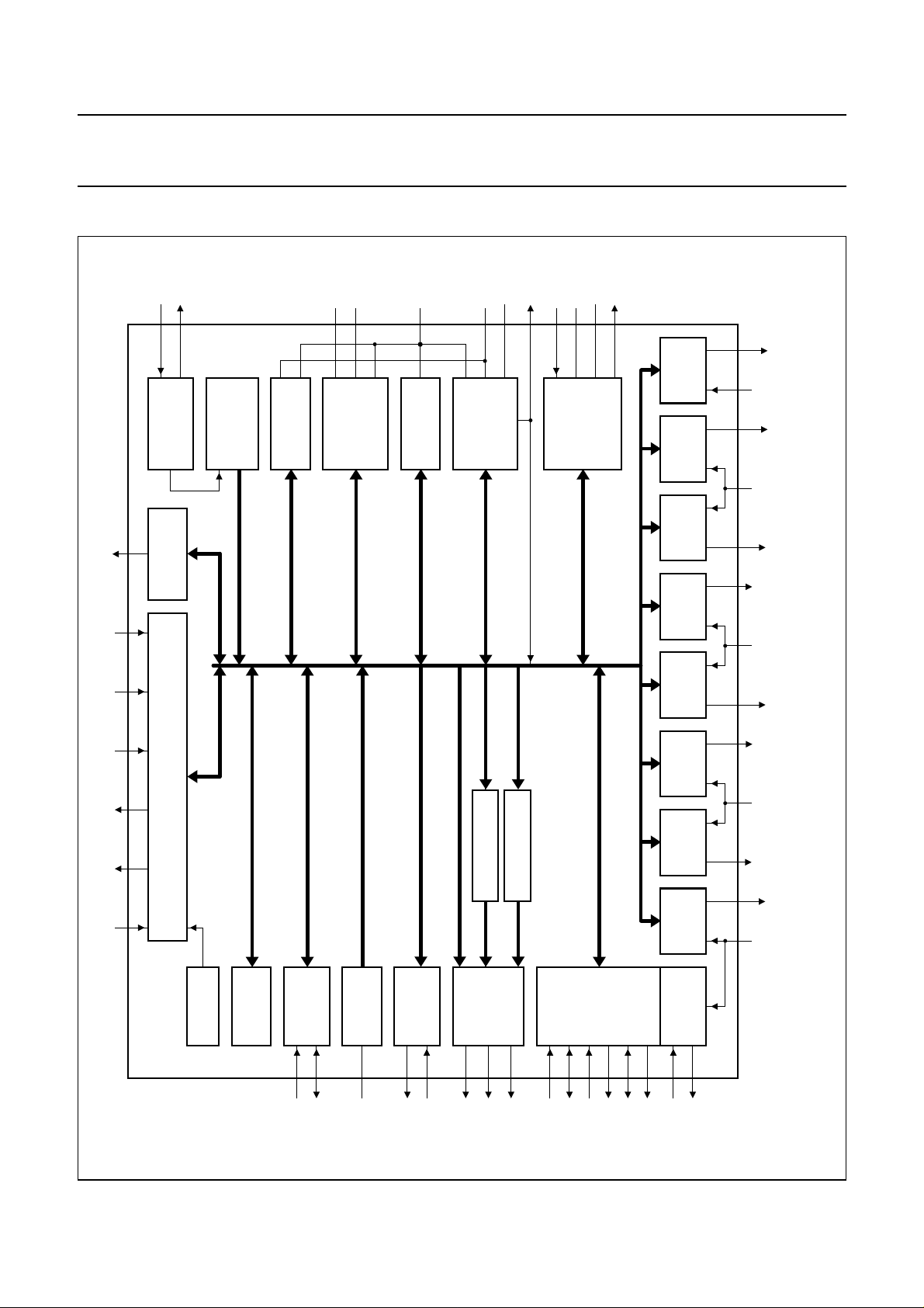
6 BLOCK DIAGRAM
OSCI
OSCO
25
26
UNIT
CLOCK
GENERATOR
BBC
IRQ_N
32kHz
OSCILLATOR
INT
CONTROLLER
CHGDRV
CHGCUR/
BATMAX
34
33
AND
BATMAX
COMPARATOR
MBC
31
BAT
V
BVM
SAVEVCHG
V
30
32
SUPPLY
MODULE
INTERNAL
VINT
29
CPVBAT
SCP
363738
CP
SCN
CPVDD
35
PCF50603
MDB679
HCREG
RF2REG
RF1REG
18 17
24
2320
22
19
RF1VDD RF2VDD HCVDDD3VDD
book, full pagewidth
27 11 4 6 5 101
ONKEY_N RSTHC_N CLK32K PWREN1 PWREN2 REC1_N
OOC
TS
PCF50603
system clocks
operation modes
temp_ok
ALARM
RTC AND
status data
control data
C-BUS
2
I
INTERFACE
3
2
reference voltage
bias currents
ON-CHIP
28
AUDIO
REFERENCE
DETECTION
12
13
PWM1 AND PWM2
GPO
48
47
46
internal supply
LED1 AND LED2
8
9
7
SIMI
434244
45
LPREG
D1REG
D2REG
IOREG
D3REG
SIMREG
41
LPD1VBAT LPVDD RF12VBAT HCVBAT
21
D1VDD
16
Fig.1 Block diagram.
14 15
40 39
SIMD3VBAT IOVDD IOD2VBAT D2VDD
This text is here in white to force landscape pages to be rotated correctly when browsing through the pdf in the Acrobat reader.This text is here in
_white to force landscape pages to be rotated correctly when browsing through the pdf in the Acrobat reader.This text is here inThis text is here in
white to force landscape pages to be rotated correctly when browsing through the pdf in the Acrobat reader. white to force landscape pages to be ...
2003 Oct 31 6
SCL
SDA
REFC
REC2_N
MICBIAS
GPO1
GPO2
GPO3
SIMIOHC
SIMCKHC
SIMIOCD
SIMCKCD
SIMRSHC_N
SIMEN
SIMVCC
SIMRSCD_N
Page 7

Philips Semiconductors Preliminary specification
Controller for power supply
PCF50603
and battery management
7 PINNING
SYMBOL PIN SUPPLY DESCRIPTION
VSS and
REFGND
− n.a. ground and VSS pads of all modules are connected to the ground plane of the
package
REC1_N 1 VINT accessory recognition input with debounce filter (active LOW); input with internal
pull-up resistor to VINT
2
SCL 2 IOVDD I
SDA 3 IOVDD I
C-bus clock input
2
C-bus data input and output
CLK32K 4 IOVDD 32.768 kHz digital clock output; in ACTIVE state and IOVDD is on
PWREN2 5 IOVDD control signal input; selects in combination with PWREN1 the ON, OFF or ECO
mode of the linear regulators
PWREN1 6 IOVDD control signal input; selects in combination with PWREN2 the ON, OFF or ECO
mode of the linear regulators
SIMRSHC_N 7 IOVDD SIM reset input from host controller (active LOW)
SIMCKHC 8 IOVDD SIM clock input from host controller
SIMIOHC 9 IOVDD SIM I/O data to or from the host controller with an internal pull-up resistor to
IOVDD
IRQ_N 10 IOVDD interrupt request output to host controller (active LOW); open-drain output with an
internal pull-up resistor to IOVDD
RSTHC_N 11 IOVDD reset output to host controller (active LOW)
MICBIAS 12 n.a. microphone bias output voltage
REC2_N 13 MICBIAS accessory recognition input with debounce filter and programmable threshold
(active LOW)
IOVDD 14 n.a. IOREG output voltage
IOD2VBAT 15 n.a. IOREG and D2REG input voltage
D2VDD 16 n.a. D2REG output voltage
HCVDD 17 n.a. HCREG output voltage
HCVBAT 18 n.a. HCREG input voltage
LPVDD 19 n.a. LPREG output voltage
LPD1VBAT 20 n.a. LPREG and D1REG input voltage
D1VDD 21 n.a. D1REG output voltage
RF1VDD 22 n.a. RF1REG output voltage
RF12VBAT 23 n.a. RF1REG and RF2REG input voltage
RF2VDD 24 n.a. RF2REG output voltage
OSCO 25 VINT 32.768 kHz oscillator output
OSCI 26 VINT 32.768 kHz oscillator input
ONKEY_N 27 VINT On-key (active LOW); input with internal pull-up resistor to VINT
REFC 28 n.a. reference voltage bypass capacitor connection
VINT 29 n.a. internal supply voltage output
V
V
V
SAVE
BAT
CHG
30 n.a. backup battery supply voltage
31 n.a. main battery supply voltage
32 n.a. charger voltage
(1)
2003 Oct 31 7
Page 8

Philips Semiconductors Preliminary specification
Controller for power supply
PCF50603
and battery management
SYMBOL PIN SUPPLY DESCRIPTION
CHGDRV 33 n.a. drive of external charger circuitry (configuration CCCV)
CHGCUR/
BATMAX
CPVDD 35 n.a. charge pump output voltage
CPVBAT 36 n.a. charge pump input voltage
SCP 37 n.a. switching capacitor positive side
SCN 38 n.a. switching capacitor negative side
D3VDD 39 n.a. D3REG output voltage
SIMD3VBAT 40 n.a. SIMREG and D3REG input voltage
SIMVCC 41 n.a. SIMREG output voltage
SIMIOCD 42 SIMVCC SIM I/O data to/from the SIM card; internal pull-up resistor to SIMVCC
SIMCKCD 43 SIMVCC SIM clock output to the SIM card
SIMRSCD_N 44 SIMVCC SIM reset output to the SIM card (active LOW)
SIMEN 45 IOVDD enable SIMI and SIMREG
GPO3 46 n.a. general purpose open-drain output 3
GPO2 47 n.a. general purpose open-drain output 2
GPO1 48 n.a. general purpose open-drain output 1
34 n.a. configuration CCCV: charger current feedback
configuration BATMAX: open-drain output of BATMAX comparator
(1)
Note
1. One ESD diode reverse biased to VSSexcept pin V
between pad and VSS.
who has one clamp in series with a 500 Ω resistor connected
CHG
2003 Oct 31 8
Page 9

Philips Semiconductors Preliminary specification
Controller for power supply
and battery management
handbook, full pagewidth
MICBIAS
RSTHC_N
IRQ_N
SIMIOHC
SIMCKHC
SIMRSHC_N
PWREN1
PWREN2
CLK32K
SDA
SCL
REC1_N
LPVDD
HCVDD
REC2_N
IOVDD
IOD2VBAT
1314151617181920212223
12 25
11 26
10 27
9 28
8 29
7 30
6 31
5 32
4 33
3 34
2 35
1 36
4847464544434241403938
GPO3
GPO1
GPO2
HCVBAT
D2VDD
PCF50603HN
SIMEN
SIMCKCD
SIMRSCD_N
LPD1VBAT
SIMVCC
SIMIOCD
D1VDD
RF12VBAT
RF1VDD
SCN
D3VDD
SIMD3VBAT
RF2VDD
24
37
SCP
OSCO
OSCI
ONKEY_N
REFC
VINT
V
SAVE
V
BAT
V
CHG
CHGDRV
CHGCUR/BATMAX
CPVDD
CPVBAT
MDB680
PCF50603
Bottom view.
All GND and VSS pads are connected to the ground plane.
Fig.2 Pin configuration.
2003 Oct 31 9
Page 10

Philips Semiconductors Preliminary specification
Controller for power supply
and battery management
8 FUNCTIONAL DESCRIPTION
8.1 On/off control
8.1.1 OPERATING STATES
The PCF50603 has four operating states (see Fig.3):
• NOPOWER
• SAVE
• STANDBY
• ACTIVE.
handbook, full pagewidth
SAVE
V
< V
BAT
VERY_LOW_BAT
V
SAVE
V
CHG
AND
> V
VERY_LOW_BACK
OR
> V
VERY_LOW_BAT
V
V
SAVE
V
BAT
CHG
NOPOWER
< V
< V
< V
PCF50603
VERY_LOW_BAT
AND
VERY_LOW_BACK
AND
VERY_LOW_BAT
Fig.3 State diagram.
8.1.2 RESET GENERATION
TheOOC generates an internal and an external reseteach
time the system goes from STANDBY to ACTIVE state. All
registersfor the regulators and convertersarereset to their
default values.
STANDBY
V
> V
BAT
VERY_LOW_BAT
ACTIVE
V
> V
BAT
LOW_BAT
MDB681
The RSTHC_N is kept LOW for minimum 10 ms after
entering the ACTIVE state. If the IOREG supply is
switched off, RSTHC_N becomes LOW again (see Fig.4).
A special condition occurs when the main battery voltage
drops below the V
VERY_LOW_BAT
limit of typically 2.7 V; the
RSTHC_N is asserted in order to shut down the host
controller immediately (see Fig.5).
2003 Oct 31 10
Page 11

Philips Semiconductors Preliminary specification
Controller for power supply
and battery management
handbook, full pagewidth
system
state
RSTHC_N
xxVDD
32 kHz
oscillator
CLK32K
Before the supplies are turned on, the internal 32 kHz clock is already stable. After
power up of the IOVDD supply the external clock on pin CLK32K becomes available.
STANDBY STANDBYACTIVE
t
= 10 ms
reset
PCF50603
MDB682
handbook, full pagewidth
system
state
RSTHC_N
SIM activation
xxVDD
32 kHz
oscillator
CLK32K
Fig.4 Reset generation timing diagram (STANDBY - ACTIVE - STANDBY transition).
STANDBY STANDBYACTIVE
t
= 10 ms
reset
SIM emergency deactivation
MDB683
Before the supplies are turned on, the internal 32 kHz clock is already stable. After
power up of the IOVDD supply the external clock on pin CLK32K becomes available.
Fig.5 Reset generation timing diagram (STANDBY - ACTIVE - STANDBY transition).
2003 Oct 31 11
Page 12

Philips Semiconductors Preliminary specification
Controller for power supply
and battery management
8.1.3 WATCHDOG TIMER
The OOC contains a WatchDog Timer (WDT). By default
it is not activated. It can be activated by setting
bit WDT_RST in the OOCC register to logic 1. Once this
bithasbeenset,the watchdog is enabled, and needs to be
cleared once every eight seconds. If the watchdog is not
reset in time, the PCF50603 automatically goes to the
STANDBY state when the watchdog timer expires. Status
bit WDTEXP is set when the watchdog timer expires. After
each ACTIVE to STANDBY transition the WDT is disabled
and needs to be activated again by software when
entering the ACTIVE state.
8.1.4 AUTOMATIC RESTART AFTER BATTERY REMOVAL
The PMU allows for an automatic restart from SAVE to
ACTIVE state when the main battery is removed for a
period less than two seconds (t
BATRMLIM
especially convenient to avoid accidental switch-off of the
). This feature is
PCF50603
phone due to mechanical bounce on the battery. The
automatic restart is enabled or disabled by control
bit BATRM_EN in the OOCC register. By default this
automatic restart feature is disabled.
Status bit BATRMSTAT in the OOCS2 register indicates
whetherthe PMU returned to ACTIVE stateduetoa restart
after battery removal. The status bit remains active until
the PMU returns to STANDBY or SAVE state.
Figure 6 shows the timing for an automatic restart due to
battery removal.
This feature is only triggered by battery removal
(V
< 2.7 V). All other shut-down conditions like, low
BAT
battery, high temperature, programming GO_STDBY do
not trigger this function.
This feature is only applicable upon the condition that a
BBC (V
SAVE>VVERY_LOW_BACK
) is available in the system.
handbook, full pagewidth
(internal status bit)
system
state
V
BAT
V
SAVE
CLK32K
RSTHC_N
xxVDD
BATRMSTAT
ACTIVE
V
LOW_BAT
V
VERY_LOW_BAT
V
LOW_BACK
SAVE
<t
BATRMLIM
t
reset
ACTIVE
MCE539
Fig.6 Automatic restart after battery removal.
2003 Oct 31 12
Page 13

Philips Semiconductors Preliminary specification
Controller for power supply
PCF50603
and battery management
8.1.5 DEBOUNCE FILTERS
Fig.7 is applicable for all debounce filters in the PCF50603.
handbook, full pagewidth
The debounced signal keeps the old value until the new value has been stable for at least the applicable debounce time. Any spike (>30 ms) in the
original signal will reset the debounce timer again. This filter suppresses all signal changes that are shorter than the debounce time.
un-debounced
debounced
interrupts
t
debounce
falling edge
Fig.7 Definition of debounce filter.
t
debounce
rising edge
MDB684
8.2 Serial interface (I2C-bus)
The I2C-bus is the serial interface of the PCF50603.
A detailed description of the I2C-bus specification,
including applications, is given in the brochure: The
I2C-bus and how to use it, order no. 9398 393 40011 or
I2C-bus Peripherals Data Handbook IC12.
8.3 Interrupt controller (INT)
The PCF50603 uses the interrupt controller to indicate to
thesystemcontroller if the status of the PCF50603 change
and that an action of the system controller is required.
Interrupts can be generated by several modules of the
PCF50603. The interrupt generator handles all interrupts
with the same priority. Priority setting shall be done by the
system controller software.
There are no timing requirements for interrupt service
response times. All events that require immediate actions
are performed by the PCF50603 without any action by the
system controller.
The function of the interrupt module is to capture, mask
and combine the interrupt signals from the modules that
can generate an interrupt. All interrupts are combined in
the interrupt signal IRQ_N. The IRQ_N signal is
implemented as an open-drain output with an internal
pull-up resistor.
The interrupt module is powered in all states (except
NOPOWER) and retains the register values. Events that
occur in the STANDBY state, are captured and can be
read out by the system controller once the system is in the
ACTIVE state.
The IRQ_N signal is asserted in the ACTIVE state
whenever one or more PCF50603 interrupts are active.
Each interrupt register (8-bits) is cleared when it is read
(R&C) through the I
2
C-bus interface. New interrupts that
occur during a R&C action are captured in an intermediate
register (see Figs.8 and 9).
All interrupts related to shut-down conditions (LOWBAT,
ONKEY1S and HIGHTMP) are automatically cleared on a
transition from ACTIVE to STANDBY state.
All interrupts can be masked: this effectively prevents that
IRQ_N is asserted for masked interrupts. Masking is
implementedwith a mask bit in the mask registers for each
interrupt source. Nevertheless, the interrupt status
registers still provide the actual interrupt status of the
masked interrupts, which allows polling of the interrupt
status registers. Note that if the mask bit is cleared for an
active interrupt, the IRQ_N line goes LOW at the next
falling edge of the output pin CLK32K.
2003 Oct 31 13
Page 14

Philips Semiconductors Preliminary specification
Controller for power supply
and battery management
handbook, full pagewidth
IRQ_N
2
I
C-bus
read request &
address
read
INT1
PCF50603
(1)
read
INT2
read
INT3
MDB685
Read access can be done with or without incremental addressing.
(1) IRQ_N becomes inactive high as soon as the read sequence of the last INTx register containing an active interrupt starts.
Fig.8 Interrupt timing; no interrupt captured during read sequence.
handbook, full pagewidth
IRQ_N
I
2
C-bus
read request &
address
read
INT1
(1)
read
INT2
minimal 1 CLK32
read
INT3
MDB686
Read access can be done with or without incremental addressing.
(1) IRQ_N becomes inactive high as soon as the read sequence of the last INTx register containing an active interrupt starts.
Fig.9 Interrupt timing; interrupt captured during read sequence.
2003 Oct 31 14
Page 15

Philips Semiconductors Preliminary specification
Controller for power supply
PCF50603
and battery management
8.4 Power supply modules
In total 11 power supply modules are available in the PCF50603; see Table 1:
• Threeregulators for supplying the digital and analog circuitry (D1REG, D2REG and D3REG). These regulators support
the ECO mode
• One regulator for high current supply (HCREG)
• One regulator for the SIMI supply (SIMREG)
• One charge pump (CP)
• One regulator for supplying the I/O pads (IOREG). This regulator supports the ECO mode
• One regulator for low power supply (LPREG). This regulator supports the ECO mode, the LPREG is the only regulator
that can be enabled in SAVE and STANDBY state (ECO mode only)
• Two low-noise regulators for RF supply (RF1REG and RF2REG)
• One ultra low-noise regulator for supplying a microphone (MBGEN).
Table 1 Power supply modules; VSS= REFGND = GND = 0 V; T
SUPPLY
NAME
NOMINAL
CURRENT
(mA)
MINIMUM
VOLTAGE
(V)
MAXIMUM
VOLTAGE
(V)
VOLTAGE
STEPS
(mV)
= −40 °C to +85 °C; unless otherwise specified.
amb
RESET
VOLTAGE
(V)
ECO
MODE
PSRR
(dB)
SIZEEXTERNAL
(1)
CAPACITOR
(nF)
(2)
Programmable power supplies
D1REG 150 1.20 3.20 100 note 3 yes 60 470
D3REG 100 1.20 3.20 100 note 3 yes 60 470
(6)
(4)
2.60 3.20 200 note 3 no 60 4700
(5)
60 1000
3.50 5.00 500 note 3 no − 220/4700
(7)
HCREG 250
SIMREG 20 1.80 3.00 − 1.8 yes
CP 75
Fixed power supplies, mask programmable
D2REG 150 1.20 3.20 100 note 3 yes 60 470
IOREG 150 1.20 3.20 100 note 3 yes 60 470
LPREG 100 1.20 3.20 100 note 3 yes 60 470
RF1REG
RF2REG
(8)
(8)
100 2.60 3.00 100 note 3 no 70 4700
100 2.60 3.00 100 note 3 no 70 4700
Fixed power supply
MBGEN 1.5 2.15 2.15 − 2.15 yes 110 4700
Notes
1. Typical value, 100 Hz < f < 1000 Hz.
2. Typical values assume X5R or X7R type of capacitor.
3. Mask programmable for reset settings of different types.
4. Under specific conditions a nominal current of 300 mA can be delivered.
5. When SIMI is in Power-down mode.
6. Maximum current depends on the selected output voltage. At 3.50 V, 4.00 V and 4.50 V the maximum output current
is 75 mA. At 5.00 V output voltage the maximum output current is 50 mA.
7. The CP module requires both a switching capacitor as well as an output capacitor.
8. Optimized for low noise (30 µV RMS value, 400 Hz < f < 80 kHz).
2003 Oct 31 15
Page 16

Philips Semiconductors Preliminary specification
Controller for power supply
and battery management
8.5 Main battery charger (MBC)
The main battery charger (MBC) module provides a
completeconstant-current/constant-voltage linear charger
controller for lithium-ion (Li-ion) batteries (in CCCV
configuration) or a programmable battery threshold level
detector for end-of-charge indication (configuration
BATMAX). Nickel-cadmium (NiCd) and Nickel metal
hydride (NiMH) batteries can also be charged with
constant current.
Only an external power PNP transistor is required to
control the charge current. The CC and CCCV control
circuitry is fully integrated in the PCF50603 charging
module.
In CCCV configuration the charging process for
Li-ion/Li-pol batteries is performed under control of the
host controller. The communication between the
PCF50603 charger module and the host controller is
interrupt based, which simplifies the control of the
PCF50603.
PCF50603
The fast charge current is determined by the value of the
external sense resistor. The charge current in the pre and
trickle charge phase is programmable as a ratio of the fast
charge current.
In BATMAX configuration an end-of-charge indication is
available on the BATMAX pin.
8.5.1 SUPPORTED CHARGER PLUGS
The PCF50603 charger circuitry supports the following
type of charger plugs (see Fig.10):
• Regulated charger plugs with output voltage at least
0.5 V above the battery voltage with a maximum of 10 V
and with current limitation up to 3C of the used battery
(CCCV and BATMAX configuration)
• Non regulated charger plugs with peak output voltages
up to 20 V with a duration of less than 14 ms and with
current limitation up to 3C of the used battery (BATMAX
configuration only).
handbook, full pagewidth
10 V
2.7 V
V
CHG
Regulated charger plug. Non regulated charger plug.
I
CHG
15 V
10 V
2.7 V
V
CHG
< 14 ms
Fig.10 Characteristics of the supported charger plugs.
< 14 ms
t
MDB687
2003 Oct 31 16
Page 17

Philips Semiconductors Preliminary specification
Controller for power supply
and battery management
8.5.2 EXTERNAL COMPONENTS
A small discrete circuit must be used to control the charge current (see Fig.11).
handbook, halfpage
(1) The charge switch requires a current gain in the range of 50 to 400 for stable loop operation.
Fig.11 Charge current external circuitry.
V
CHG
CHGDRV
CHGCUR
V
BAT
0.15 Ω
BC869
R
sense
(1)
MDB688
PCF50603
8.6 Backup battery charger (BBC)
The BBC is implemented as a voltage limited current
source with a selectable output resistor. It offers the
following features:
• Selectableoutput resistor to reduce the current at higher
voltages
• Four programmable charge currents
• Two programmable maximum limiting voltages
• The BBC can be enabled in the ACTIVE state; in all
other states the BBC is disabled.
8.7 SIM card interface (SIMI)
The SIMI provides the facilities to communicate with SIM.
It offers the following features:
• Support for transparent mode. The host controller
controls the communication with the SIM card, including
the activation and deactivation sequences.
• Support for sequencer mode. The internal sequencer of
the PCF50603 performs the activation and deactivation
sequences.
• Includes a dedicated linear regulator for the SIM card
supply(SIMREG) supporting both 1.8 V and 3.0 V cards
• Provides level-shifters for the SIM interfacing signals.
The level-shifters translate the host controller signal
levels (IOVDD) to SIM card signal levels (SIMVCC) and
vice versa.
• In transparent mode the SIMEN input allows the host
controller to have direct control over the SIM card
supply. In sequencer mode the SIMEN input indicates
the presence of a SIM card.
• Enhanced ESD protection on all SIM contact pins
• The SIMI and SIMREG can be enabled in the ACTIVE
state. In all other states the SIMI and SIMREG are
disabled.
8.8 Battery voltage monitor (BVM)
The BVM monitors the main battery voltage. It offers the
following features:
• Programmable low battery threshold (V
LOW_BAT
)
• Hysteresis and selectable debounce filter built in to
prevent fast cycling
• The BVM is enabled in all activity states.
The BVM observes permanently the main battery voltage
and generates a LOWBAT interrupt if the battery voltage
drops below the programmed threshold voltage V
LOW_BAT
(see Fig.12). When a LOWBAT interrupt is generated in
ACTIVE state, the host controller should initiate a
transition to STANDBY state. In case the host controller
does not initiate a transition to the STANDBY state within
eight seconds after the interrupt occurred, the OOC forces
the PCF50603 to the STANDBY state in order to prevent a
too deep discharge of the battery.
2003 Oct 31 17
Page 18

Philips Semiconductors Preliminary specification
Controller for power supply
and battery management
handbook, full pagewidth
V
LOW_BAT
8.9 Temperature high sensor (TS)
The TS monitors the junction temperature of the
PCF50603. It offers the following features:
• Fixed temperature threshold
• Hysteresis and debounce filter built in to prevent fast
cycling
• The TS is enabled in ACTIVE state, in all other states
the TS is disabled.
The behaviour of the TS is shown in Figure 13.
V
BAT
LOWBAT
interrupt
V
Fig.12 BVM and LOWBAT behaviour.
PCF50603
V
hys
t
debounce
t
MDB689
A HIGHTMP interrupt is generated when the temperature
threshold is passed for more than 62 ms (debouncing
time). When a HIGHTMP interrupt is generated the host
controller should initiate a transition to STANDBY state.
In case the host controller does not initiate a transition to
the STANDBY state within 1 second after the interrupt
occurred,theOOCforcesthe PCF50603 to the STANDBY
state in order to prevent damage to the circuit.
The hysteresis and debounce time have been built in to
prevent fast cycling of the HIGHTMP signal.
The TS can not be disabled via the I2C-bus.
handbook, full pagewidth
150 °C
130
HIGHTMP
interrupt
°C
T
j
t
debounce
Fig.13 TS behaviour.
2003 Oct 31 18
T
hys
t
debounce
t
MDB690
Page 19

Philips Semiconductors Preliminary specification
Controller for power supply
and battery management
8.10 Real time clock (RTC)
The RTC module provides the time information to the
handset based on a 1 Hz clock frequency. Basically it is a
32-bit counter counting elapsed seconds.
• The RTC module contains one alarm function that
generates an interrupt if the actual RTC time equals the
content of the alarm register. The alarm registers are
preset to all 1 s which effectively disables the alarm;
effectively no alarm interrupt will be generated as long
as the RTC counter does not overflow. It is
recommended to mask the ALARM interrupt before a
new value is written to the alarm registers, in order to
preventinterrupts during the write actions (a new setting
may require up to 4 register writes).
• The RTC module is able to generate an interrupt each
second (SECOND interrupt) as well as each minute
(MINUTE interrupt). When the RTC starts up the first
time (after transition from NOPOWER state) the minute
interruptis aligned with each 60 seconds crossing. If the
synchronization with the 60 second crossing is required
after reprogramming the RTC time registers it is up to
the software to program the RTC time registers with a
modulo 60 value.
PCF50603
8.12 LED modulator (LED1 and LED2)
The PCF50603 contains two LED modulators (LED1 and
LED2), which can be selected as input for any of the GPO
outputs. The LED modulator of the PCF50603 is used for
the control of the indicator LEDs. They offer the following
features:
• The LED driver can select eight different repetition
periods
• Capable of generating eight different blinking patterns.
The selected pattern is generated once per repetition
period
• The LED can be used as a status indicator during the
ACTIVE state or when a charger is connected.
8.13 General purpose outputs (GPO)
The PCF50603 contains three high current (100 mA)
open-drain GPOs. They offer the following features:
• Each GPO can be configured as a constant LOW level,
a high impedance, a LED modulator output, a PWM
output or as the complementary PWM output PWM
• The GPOs can sink 100 mA from any supply or battery
voltage.
8.11 Pulse-width modulator (PWM1 and PWM2)
The two PWMs (PWM1 and PWM2) offer the following
features:
• Programmable frequency and duty cycle
• Any of the GPOs can be connected to either the PWMs
or the inverse of the PWMs
• The PWMs can be independently enabled in ACTIVE
state. In all other states the PWMs are disabled.
2003 Oct 31 19
Page 20

Philips Semiconductors Preliminary specification
Controller for power supply
PCF50603
and battery management
9 LIMITING VALUES
In accordance with the Absolute Maximum Rating System (IEC 60134).
SYMBOL PARAMETER CONDITIONS MIN. MAX. UNIT
V
V
V
V
I
I
I
O
P
T
T
V
BAT
SAVE
CHG
I
tot
amb
stg
esd
main battery voltage −0.5 +6.5 V
backup battery input voltage −0.5 +6.5 V
charger input voltage −0.5 +20 V
input voltage on any pin with
−0.5 +6.5 V
respect to REFGND
input current at any input −10 +10 mA
output current at any output −10 +10 mA
total power dissipation − 2000 mW
operating ambient
−40 +85 °C
temperature
storage temperature −55 +150 °C
electrostatic discharge
voltage
HBM; note 1
pins SIMEN, IOD2VBAT, SIMD3VBAT,
−±6000 V
SIMRSCD_N, SIMCKCD, SIMIOCD,
V
, V
BAT
, CPVBAT, LPD1VBAT,
SAVE
REC1_N, SIMVCC, RF12VBAT,
HCVBAT, REC2_N
pin V
CHG
−±4000 V
other pins −±2000 V
MM; note 2 −±200 V
Notes
1. Human Body Model: equivalent to discharging a 100 pF capacitor via a 1.5 kΩ resistor.
2. Machine Model: equivalent to discharging a 200 pF capacitor via a 0 Ω resistor.
10 CHARACTERISTICS
V
= REFGND = GND = 0 V; T
SS
= −40 °C to +85 °C; unless otherwise specified.
amb
SYMBOL PARAMETER CONDITIONS MIN. TYP. MAX. UNIT
V
V
V
BAT
SAVE
CHG
main battery input voltage 0 − 5.7 V
backup battery input voltage 0 − 5.7 V
charger input voltage DC 0 − 15.0 V
rectified sine wave;
0 − 20.0 V
100 Hz to 120 Hz; note 1
V
CHGMIN
minimum charger voltage
− 2.7 − V
enabling MBC module
f
CLKCCO
high clock frequency 32 kHz clock available 3.42 3.6 3.78 MHz
D1 regulator
V
O
I
O
output voltage 1.20 − 3.20 V
output current −−150 mA
2003 Oct 31 20
Page 21

Philips Semiconductors Preliminary specification
Controller for power supply
PCF50603
and battery management
SYMBOL PARAMETER CONDITIONS MIN. TYP. MAX. UNIT
D3 regulator
V
O
I
O
HC regulator
V
O
I
O
SIM regulator
V
O
I
O
CP regulator
V
O
I
O
D2 regulator
V
O
I
O
IO regulator
V
O
I
O
LP regulator
V
O
I
O
RF1 regulator
V
O
I
O
RF2 regulator
V
O
I
O
MBGEN regulator
V
O
I
O
Notes
1. Under specific conditions a nominal current of 300 mA can be delivered.
2. Maximum current depends on the selected output voltage. At 3.50 V, 4.00 V and 4.50 V the maximum output current
is 75 mA. At 5.00 V output voltage the maximum output current is 50 mA.
output voltage 1.20 − 3.20 V
output current −−100 mA
output voltage 2.60 − 3.20 V
output current note 1 −−250 mA
output voltage 1.80 − 3.00 V
output current −−20 mA
output voltage 3.50 − 5.00 V
output current note 2 −−75 mA
output voltage 1.20 − 3.20 V
output current −−150 mA
output voltage 1.20 − 3.20 V
output current −−150 mA
output voltage 1.20 − 3.20 V
output current −−100 mA
output voltage 2.60 − 3.00 V
output current −−100 mA
output voltage 2.60 − 3.00 V
output current −−100 mA
output voltage 2.15 − 2.15 V
output current −−1.5 mA
2003 Oct 31 21
Page 22

Philips Semiconductors Preliminary specification
Controller for power supply
and battery management
11 APPLICATION INFORMATION
handbook, full pagewidth
MAIN
BATTERY
2.2 µF
V
CHG
RF1VDD
RF2VDD
SCP
SCN
CPVDD
GPO3
GPO2
GPO1
OSCI
OSCO
SIMEN
SIMVCC
V
BAT
31
34
33
32
27
22
24
37
38
35
46
47
48
26
25
45
44
42
43
41
BATTERY
CHARGER
CONSTANT
CURRENT
RF
UNIT
back light
back light
32.768 kHz
IOVDD
card present
SIM
CARD
READER
+
−
EL lamp
2.2 µF
or
DC
10 MΩ
DC
R
SENSE
(3)
on key
4700 nF
4700 nF
220 nF
4700 nF
10 pF
10 pF
10 kΩ
SIMRSCD_N
1000 nF
CHGCUR
CHGDRV
ONKEY_N
SIMIOCD
SIMCKCD
RF12VBAT
23
LPD1VBAT
20
IOD2VBAT
15
PCF50603
REFGND/V
SIMD3VBAT
40
SS
CPVBAT
36
HCVBAT
18
30
29
28
12
17
19
13
1
21
14
16
39
6
5
11
10
4
3
2
9
8
7
V
SAVE
VINT
REFC
MICBIAS
HCVDD
LPVDD
REC2_N
REC1_N
D1VDD
IOVDD
D2VDD
D3VDD
PWREN1
PWREN2
RSTHC_N
IRQ_N
CLK32K
SDA
SCL
SIMIOHC
SIMCKHC
SIMRSHC_N
battery
backup
470 nF
100 nF
4700
nF
(1)
4700
nF
(2)
470
nF
headset
from bottom
connector
470 nF
470 nF
470 nF
470 nF
1 kΩ 1 kΩ
revmod
PCF50603
RAM 1.8 V
FLASH 1.8 V
AUXADCx
MICP
MICN
VDDA
VDDD
PCF5213
VDDE3
VDDA
VDDC
VDDE1
VDDE2
LOWVOLT_N
ONKEY
AUXON_N
GPON0
RFSIGx
RSTON
SIMERRN
CLK32I
SDA
SCL
SIMIO
SIMCLK
GPOx
MDB691
(1) HCVDD is reserved for hands free audio supply.
(2) LPVDD not used in the system.
(3) Connect V
to ground if charger is used in BATMAX configuration.
CHG
Fig.14 Application diagram.
2003 Oct 31 22
Page 23

Philips Semiconductors Preliminary specification
Controller for power supply
and battery management
12 PACKAGE OUTLINE
HVQFN48: plastic thermal enhanced very thin quad flat package; no leads;
48 terminals; body 6 x 6 x 0.85 mm
A
D
terminal 1
index area
B
E
A
PCF50603
SOT778-1
A
1
detail X
c
e
1
D
4.25
3.95
1/2 e
b
25
1/2 e
36
E
4.25
3.95
37
scale
h
e
1
4.4
0.41
D
h
0 2.5 5 mm
(1)
E
h
6.1
5.9
REFERENCES
e
13 24
L
12
E
h
1
terminal 1
index area
DIMENSIONS (mm are the original dimensions)
Note
1. Plastic or metal protrusions of 0.075 mm maximum per side are not included.
(1)
A
UNIT
mm
OUTLINE
VERSION
SOT778-1 - - -- - - - - -
max.
A
0.05
0.00
1
48
bc
0.25
0.15
(1)
D
6.1
0.2
5.9
IEC JEDEC JEITA
e
v
w
e
4.4
C
y
w
C
1
ye
0.05 0.1
EUROPEAN
PROJECTION
y
1
M
ACCB
M
e
2
L
2
0.5
0.1v0.05
0.3
y
X
ISSUE DATE
02-07-05
2003 Oct 31 23
Page 24

Philips Semiconductors Preliminary specification
Controller for power supply
and battery management
13 SOLDERING
13.1 Introduction to soldering surface mount
packages
Thistext gives a very brief insight to a complex technology.
A more in-depth account of soldering ICs can be found in
our
“Data Handbook IC26; Integrated Circuit Packages”
(document order number 9398 652 90011).
There is no soldering method that is ideal for all surface
mount IC packages. Wave soldering can still be used for
certainsurface mount ICs, but it is not suitable forfinepitch
SMDs. In these situations reflow soldering is
recommended.
13.2 Reflow soldering
Reflow soldering requires solder paste (a suspension of
fine solder particles, flux and binding agent) to be applied
totheprinted-circuitboardby screen printing, stencilling or
pressure-syringe dispensing before package placement.
Driven by legislation and environmental forces the
worldwide use of lead-free solder pastes is increasing.
Several methods exist for reflowing; for example,
convection or convection/infrared heating in a conveyor
type oven. Throughput times (preheating, soldering and
cooling) vary between 100 and 200 seconds depending
on heating method.
Typical reflow peak temperatures range from
215 to 270 °C depending on solder paste material. The
top-surface temperature of the packages should
preferably be kept:
• below 220 °C (SnPb process) or below 245 °C (Pb-free
process)
– for all BGA and SSOP-T packages
– for packages with a thickness ≥ 2.5 mm
– for packages with a thickness < 2.5 mm and a
volume ≥ 350 mm3 so called thick/large packages.
• below 235 °C (SnPb process) or below 260 °C (Pb-free
process) for packages with a thickness < 2.5 mm and a
volume < 350 mm3 so called small/thin packages.
Moisture sensitivity precautions, as indicated on packing,
must be respected at all times.
13.3 Wave soldering
Conventional single wave soldering is not recommended
forsurface mount devices (SMDs) or printed-circuit boards
PCF50603
with a high component density, as solder bridging and
non-wetting can present major problems.
To overcome these problems the double-wave soldering
method was specifically developed.
If wave soldering is used the following conditions must be
observed for optimal results:
• Use a double-wave soldering method comprising a
turbulent wave with high upward pressure followed by a
smooth laminar wave.
• For packages with leads on two sides and a pitch (e):
– larger than or equal to 1.27 mm, the footprint
longitudinal axis is preferred to be parallel to the
transport direction of the printed-circuit board;
– smaller than 1.27 mm, the footprint longitudinal axis
must be parallel to the transport direction of the
printed-circuit board.
The footprint must incorporate solder thieves at the
downstream end.
• Forpackages with leads on four sides, the footprint must
be placed at a 45° angle to the transport direction of the
printed-circuit board. The footprint must incorporate
solder thieves downstream and at the side corners.
During placement and before soldering, the package must
be fixed with a droplet of adhesive. The adhesive can be
applied by screen printing, pin transfer or syringe
dispensing. The package can be soldered after the
adhesive is cured.
Typical dwell time of the leads in the wave ranges from
3 to 4 seconds at 250 °C or 265 °C, depending on solder
material applied, SnPb or Pb-free respectively.
A mildly-activated flux will eliminate the need for removal
of corrosive residues in most applications.
13.4 Manual soldering
Fix the component by first soldering two
diagonally-opposite end leads. Use a low voltage (24 V or
less) soldering iron applied to the flat part of the lead.
Contact time must be limited to 10 seconds at up to
300 °C.
When using a dedicated tool, all other leads can be
soldered in one operation within 2 to 5 seconds between
270 and 320 °C.
2003 Oct 31 24
Page 25

Philips Semiconductors Preliminary specification
Controller for power supply
PCF50603
and battery management
13.5 Suitability of surface mount IC packages for wave and reflow soldering methods
PACKAGE
BGA, LBGA, LFBGA, SQFP, SSOP-T
DHVQFN, HBCC, HBGA, HLQFP, HSQFP, HSOP, HTQFP,
(1)
(3)
, TFBGA, VFBGA not suitable suitable
not suitable
HTSSOP, HVQFN, HVSON, SMS
(5)
PLCC
, SO, SOJ suitable suitable
LQFP, QFP, TQFP not recommended
SSOP, TSSOP, VSO, VSSOP not recommended
(8)
PMFP
not suitable not suitable
Notes
1. FormoredetailedinformationontheBGApackagesrefer to the
“(LF)BGAApplicationNote
from your Philips Semiconductors sales office.
2. All surface mount (SMD) packages are moisture sensitive. Depending upon the moisture content, the maximum
temperature (with respect to time) and body size of the package, there is a risk that internal or external package
cracks may occur due to vaporization of the moisture in them (the so called popcorn effect). For details, refer to the
Drypack information in the
“Data Handbook IC26; Integrated Circuit Packages; Section: Packing Methods”
3. These transparent plastic packages are extremely sensitive to reflow soldering conditions and must on no account
be processed through more than one soldering cycle or subjected to infrared reflow soldering with peak temperature
exceeding 217 °C ± 10 °C measured in the atmosphere of the reflow oven. The package body peak temperature
must be kept as low as possible.
4. These packages are not suitable for wave soldering. On versions with the heatsink on the bottom side, the solder
cannot penetrate between the printed-circuit board and the heatsink. On versions with the heatsink on the top side,
the solder might be deposited on the heatsink surface.
5. If wave soldering is considered, then the package must be placed at a 45° angle to the solder wave direction.
The package footprint must incorporate solder thieves downstream and at the side corners.
6. Wave soldering is suitable for LQFP, TQFP and QFP packages with a pitch (e) larger than 0.8 mm; it is definitely not
suitable for packages with a pitch (e) equal to or smaller than 0.65 mm.
7. Wave soldering is suitable for SSOP, TSSOP, VSO and VSSOP packages with a pitch (e) equal to or larger than
0.65 mm; it is definitely not suitable for packages with a pitch (e) equal to or smaller than 0.5 mm.
8. Hot bar or manual soldering is suitable for PMFP packages.
SOLDERING METHOD
WAVE REFLOW
(4)
(5)(6)
(7)
suitable
suitable
suitable
”(AN01026);orderacopy
(2)
.
2003 Oct 31 25
Page 26

Philips Semiconductors Preliminary specification
Controller for power supply
PCF50603
and battery management
14 DATA SHEET STATUS
LEVEL
I Objective data Development This data sheet contains data from the objective specification for product
II Preliminary data Qualification This data sheet contains data from the preliminary specification.
III Product data Production This data sheet contains data from the product specification. Philips
Notes
1. Please consult the most recently issued data sheet before initiating or completing a design.
2. The product status of the device(s) described in this data sheet may have changed since this data sheet was
published. The latest information is available on the Internet at URL http://www.semiconductors.philips.com.
3. For data sheets describing multiple type numbers, the highest-level product status determines the data sheet status.
DATA SHEET
STATUS
(1)
PRODUCT
STATUS
(2)(3)
DEFINITION
development. Philips Semiconductors reserves the right to change the
specification in any manner without notice.
Supplementary data will be published at a later date. Philips
Semiconductors reserves the right to change the specification without
notice, in order to improve the design and supply the best possible
product.
Semiconductors reserves the right to make changes at any time in order
to improve the design, manufacturing and supply. Relevant changes will
be communicated via a Customer Product/Process Change Notification
(CPCN).
15 DEFINITIONS
Short-form specification The data in a short-form
specification is extracted from a full data sheet with the
same type number and title. For detailed information see
the relevant data sheet or data handbook.
Limiting values definition Limiting values given are in
accordance with the Absolute Maximum Rating System
(IEC 60134). Stress above one or more of the limiting
values may cause permanent damage to the device.
These are stress ratings only and operation of the device
atthese or at any other conditions above those given in the
Characteristics sections of the specification is not implied.
Exposure to limiting values for extended periods may
affect device reliability.
Application information Applications that are
described herein for any of these products are for
illustrative purposes only. Philips Semiconductors make
norepresentation or warranty that such applicationswillbe
suitable for the specified use without further testing or
modification.
16 DISCLAIMERS
Life support applications These products are not
designed for use in life support appliances, devices, or
systems where malfunction of these products can
reasonably be expected to result in personal injury. Philips
Semiconductorscustomers using or selling theseproducts
for use in such applications do so at their own risk and
agree to fully indemnify Philips Semiconductors for any
damages resulting from such application.
Right to make changes Philips Semiconductors
reserves the right to make changes in the products including circuits, standard cells, and/or software described or contained herein in order to improve design
and/or performance. When the product is in full production
(status ‘Production’), relevant changes will be
communicated via a Customer Product/Process Change
Notification (CPCN). Philips Semiconductors assumes no
responsibility or liability for the use of any of these
products, conveys no licence or title under any patent,
copyright, or mask work right to these products, and
makes no representations or warranties that these
products are free from patent, copyright, or mask work
right infringement, unless otherwise specified.
2003 Oct 31 26
Page 27

Philips Semiconductors Preliminary specification
Controller for power supply
and battery management
17 PURCHASE OF PHILIPS I2C COMPONENTS
Purchase of Philips I
components in the I2C system provided the system conforms to the I2C specification defined by
Philips. This specification can be ordered using the code 9398 393 40011.
2
C components conveys a license under the Philips’ I2C patent to use the
PCF50603
2003 Oct 31 27
Page 28

Philips Semiconductors – a w orldwide compan y
Contact information
For additional information please visit http://www.semiconductors.philips.com. Fax: +31 40 27 24825
For sales offices addresses send e-mail to: sales.addresses@www.semiconductors.philips.com.
© Koninklijke Philips Electronics N.V. 2003
All rights are reserved. Reproduction in whole or in part is prohibited without the prior written consent of the copyright owner.
The information presented in this document does not form part of any quotation or contract, is believed to be accurate and reliable and may be changed
without notice. No liability will be accepted by the publisher for any consequence of its use. Publication thereof does not convey nor imply any license
under patent- or other industrial or intellectual property rights.
Printed in The Netherlands R54/01/pp28 Date of release: 2003 Oct 31 Document order number: 9397 750 11771
SCA75
Page 29

WWW.ALLDATASHEET.COM
Copyright © Each Manufacturing Company.
All Datasheets cannot be modified without permission.
This datasheet has been download from :
www.AllDataSheet.com
100% Free DataSheet Search Site.
Free Download.
No Register.
Fast Search System.
www.AllDataSheet.com
 Loading...