

Page 1

DATA SH EET
Product specification
Supersedes data of September 1993
File under Integrated Circuits, IC16
1997 Apr 16
INTEGRATED CIRCUITS
PCF1175C
4-digit duplex LCD car clock
Page 2
1997 Apr 16 2
Philips Semiconductors Product specification
4-digit duplex LCD car clock PCF1175C
FEATURES
• Internal voltage regulator is electrically programmable
for various LCD voltages
• Time calibration is electrically programmable
(no trimming capacitor required)
• LCD voltage adjusts with temperature for good contrast
• 4.19 MHz oscillator
• 12-hour or 24-hour mode
• Operating ambient temperature: −40 to +85 °C
• 28-lead plastic SMD (SO28)
• 1 Hz set mode.
GENERAL DESCRIPTION
The PCF1175C is a single chip, 4.19 MHz CMOS car clock
circuit providing hours, minutes and seconds functions.
It is designed to drive a 4-digit duplex liquid crystal display
(LCD).
Two external single-pole, single-throw switches will
accomplish all time setting functions. Time calibration and
voltage regulator are electrically programmable via an
on-chip EEPROM. The circuit is battery-operated via an
internal voltage regulator and an external resistor.
ORDERING INFORMATION
Notes
1. See Fig.1 and Chapter “Package outline” for pin layout and package details.
2. See Chapter “Chip dimensions and bonding pad locations” for pad layout and package details.
TYPE
NUMBER
PACKAGE
NAME DESCRIPTION VERSION
PCF1175CT SO28 plastic small outline package; 28 leads; body width 7.5 mm
(1)
SOT136-1
PCF1175CU − uncased chip in tray
(2)
−
PCF1175CU/10 − chip-on-film frame carrier (FFC)
(2)
−
Page 3

1997 Apr 16 3
Philips Semiconductors Product specification
4-digit duplex LCD car clock PCF1175C
PINNING
SYMBOL PIN DESCRIPTION
S1 1 hour adjustment input
DATA 2 EEPROM data input
OSC IN 3 oscillator input
OSC OUT 4 oscillator output
V
SS
5 negative supply voltage
MODE 6 12/24-hour mode select input
V
PP
7 programming voltage input
TS 8 test speed-up mode input
ENABLE 9 enable input (for S1 and S2)
V
DD
10 positive supply voltage
FLASH 11 colon option input
SEL 12 EEPROM select input
S2 13 minute adjustment input
B4/C4 14 segment driver
G4/D4 15 segment driver
F4/E4 16 segment driver
B3/C3 17 segment driver
G3/AD3 18 segment driver
F3/E3 19 segment driver
A4/COL 20 segment driver
B2/C2 21 segment driver
G2/D2 22 segment driver
F2/E2 23 segment driver
B1/C1 24 segment driver
A2/ADEG1 25 segment driver
AM/PM 26 segment driver
BP2 27 backplane 2
BP1 28 backplane 1
Fig.1 Pin configuration, PCF1175CT, (SO28).
1
2
3
4
5
6
7
8
9
10
11
12
13
28
27
26
25
24
23
22
21
20
19
18
17
16
1514
PCF1175CT
S1
DATA
OSC OUT
SS
MODE
PP
TS
ENABLE
DD
FLASH
SEL
S2
B4/C4
V
V
V
OSC IN
G4/D4
F4/E4
B3/C3
G3/AD3
F3/E3
A4/COL
B2/C2
G2/D2
F2/E2
B1/C1
A2/ADEG1
AM/PM
BP2
BP1
MSB222
Page 4
1997 Apr 16 4
Philips Semiconductors Product specification
4-digit duplex LCD car clock PCF1175C
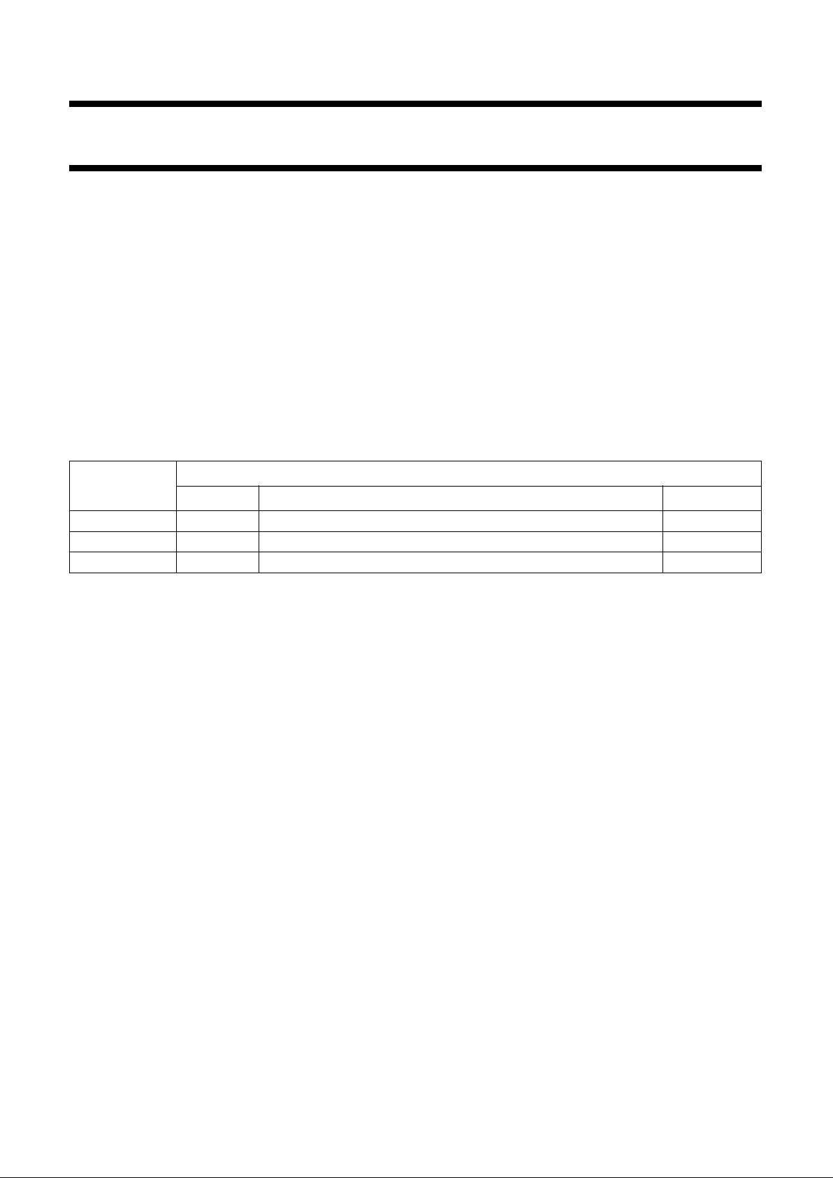
FUNCTIONAL DESCRIPTION AND TESTING
Outputs
The circuit outputs 1 : 2 multiplexed data (duplex) to the
LCD. Generation of BP1 and BP2 (three-level backplane
signals) and the output signals are shown in Fig.4.
The average voltages across the segments are:
1. V
ON(RMS)
= 0.79 V
DD
2. V
OFF(RMS)
= 0.35 VDD.
Fig.2 Segment designation of LCD.
MSA992
A2
G2
D2
F2
E2
B2
C2
P1 (P3)
P2 (P4)
A3
G3
D3
F3
E3
B3
C3
A4
G4
D4
F4
E4
B4
C4
AM
PM
A1
G1
D1
E1
B1
C1
Fig.3 Typical displays.
a. 12-hour mode.
b. 24-hour mode.
PM
TIME
MSA993
(a)
MSA994
TIME
(b)
Fig.4 Backplane and output signals.
MSB226
V
DD
VDD/2
0
BP1
V
DD
VDD/2
0
BP2
V
DD
0
SEGMENT1SEGMENT
2
ON ON
V
DD
0
OFF ON
V
DD
0
ON OFF
V
DD
0
OFF OFF
15.625 ms
Page 5
1997 Apr 16 5
Philips Semiconductors Product specification
4-digit duplex LCD car clock PCF1175C
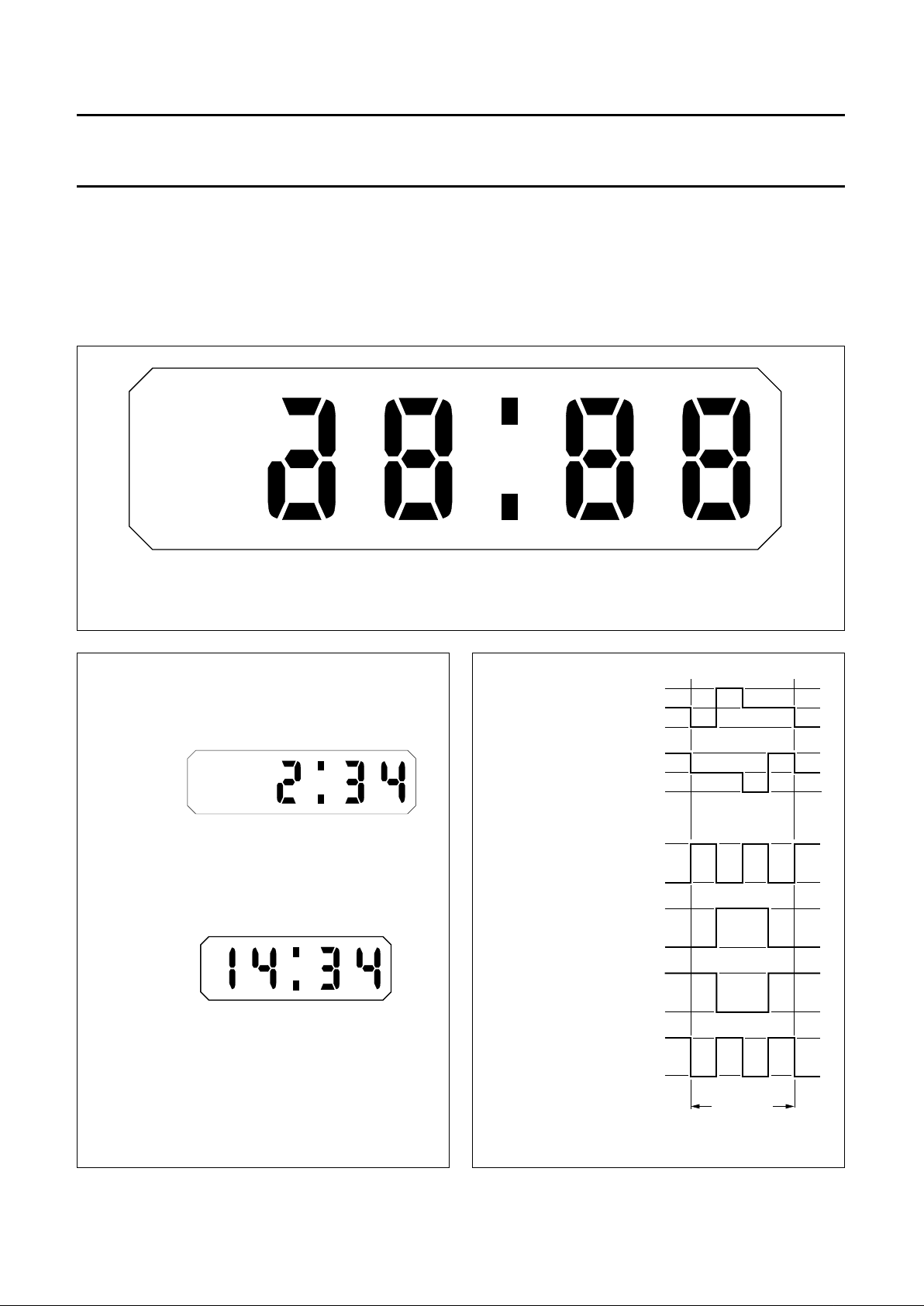
LCD voltage (see Fig.5)
The adjustable voltage regulator controls the supply
voltage (see Section “LCD voltage programming”) in
relation to temperature for good contrast, for example
when VDD= 4.5 V at +25 °C, then:
VDD= 3 to 4 V at +85 °C.
VDD= 5 to 6 V at −40 °C.
Fig.5 Regulated voltage as a function of temperature (typical).
(1) Programmed to 4.0 V at 25 °C (value within the specified operating range).
(2) Programmed to 4.5 V at 25 °C (value within the specified operating range).
(3) Programmed to 5.0 V at 25 °C (value within the specified operating range).
40 0 40 120
−8
−6
−2
0
−4
MSA995
80
T ( C)
o
V
SS
(V)
(2)
(1)
(3)
Page 6

1997 Apr 16 6
Philips Semiconductors Product specification
4-digit duplex LCD car clock PCF1175C
12/24-hour mode
Operation in 12-hour or 24-hour mode is selected by
connecting MODE to VDD or VSS respectively. If MODE is
left open-circuit and a reset occurs, the mode will change
from 12-hour to 24-hour mode or vice versa.
Power-on
After connecting the supply, the start-up mode is:
MODE connected to V
DD
: 12-hour mode, 1:00 AM.
MODE connected to VSS: 12-hour mode, 0:00.
MODE left open-circuit: 24-hour mode, 0:00 or 1:00.
Colon
If FLASH is connected to V
DD
the colon pulses at 1 Hz.
If FLASH is connected to VSS the colon is static.
Time setting
Switch inputs S1 and S2 have a pull-up resistor to facilitate
the use of single-pole, single-throw contacts. A debounce
circuit is incorporated to protect against contact bounce
and parasitic voltages.
Set enable
Inputs S1 and S2 are enabled by connecting ENABLE to
V
DD
or disabled by connecting to VSS.
Set hours
When S1 is connected to V
SS
the hours displayed
advances by one and after one second continues with one
advance per second until S1 is released (auto-increment).
Set minutes
When S2 is connected to V
SS
the time displayed in
minutes advances by one and after one second continues
with one advance per second until S2 is released
(auto-increment). In addition to minute correction, the
seconds counter is reset to zero.
Segment test/reset
When S1 and S2 are connected to V
SS
, all LCD segments
are switched ON. Releasing switches S1 and S2 resets the
display. No reset occurs when DATA is connected to V
SS
(overlapping S1 and S2).
Test mode
When TS is connected to V
DD
, the device is in normal
operating mode. When connecting TS to VSS all counters
(seconds, minutes and hours) are stopped, allowing quick
testing of the display via S1 and S2 (debounce and
auto-increment times are 64 times faster). TS has a
pull-up resistor but for reasons of safety it should be
connected to VDD.
EEPROM
V
PP
has a pull-up resistor but for reasons of safety it should
be connected to VDD.
LCD voltage programming
To enable LCD voltage programming, SEL is set to
open-circuit and a level of V
DD
− 5 V is applied to VPP (see
Fig.6). The first pulse (tE) applied to the DATA input clears
the EEPROM to give the lowest voltage output. Further
pulses (tL) will increment the output voltage by steps of
typically 150 mV (T
amb
=25°C). For programming,
measure VDD− VSS and apply a store pulse (tW) when the
required value is reached. If the maximum number of steps
(n = 31) is reached and an additional pulse is applied the
voltage will return to the lowest value.
Time calibration
To compensate for the tolerance in the quartz crystal
frequency which has been positively offset (nominal
deviation +60 × 10
−6
) by capacitors at the oscillator input
and output, a number (n) of 262144 Hz are inhibited every
second of operation.
Page 7

1997 Apr 16 7
Philips Semiconductors Product specification
4-digit duplex LCD car clock PCF1175C
The number (n) is stored in a non-volatile memory which is achieved by the following steps (see Fig.6):
1. Set SEL to VSS and a level of VDD− 5 V to V
PP
2. The quartz-frequency deviation ∆f/f is measured and (n) is calculated (see Table 1)
3. A first pulse tE is applied to the DATA input clears the EEPROM to give the highest backplane frequency
4. The calculated pulses (n) are entered in (tH, tL). If the maximum backplane period is reached and an additional pulse
is applied the period will return to the lowest value.
5. The backplane period is controlled and when correct fixed by applying the store pulse t
W
6. Release SEL and VPP.
Table 1 Time calibration (∆t = 7.63 µs; SEL at V
SS
)
OSCILLATOR-FREQUENCY DEVIATION
∆f/f
(× 10
−6
)
NUMBER OF PULSES
(n)
BACKPLANE PERIOD
(ms)
0 0 15.625
+3.8 1 15.633
+7.6 2 15.641
+11.4 3 15.648
...
...
...
+117.8 31 15.861
Page 8

1997 Apr 16 8
Philips Semiconductors Product specification
4-digit duplex LCD car clock PCF1175C
Fig.6 Programming diagram.
MSB223
PCF1175C
SEL
V
DD
OSC OUT
OSC IN
V
SS
12 V
R
6.8 kΩ
C 47 µF
ext
V
SS
DATA
V
PP
pulse
generators
0 V
t , t = 4 to 6 ms
WE
t = 1 µs
H
t = 1 to 1.5 µs
L
t
E
tHtLtHt
L
V
DD
t
H
t
W
n
clears cells incrementing counters store pulse
5 VV
DD
DATA
V
PP
V
DD
5 VV
DD
50 µs
50 µs
50 µs
50 µs
Page 9

1997 Apr 16 9
Philips Semiconductors Product specification
4-digit duplex LCD car clock PCF1175C
LIMITING VALUES
In accordance with the Absolute Maximum Rating System (IEC 134).
Note
1. Connecting the supply voltage with reverse polarity, will not harm the circuit, provided the current is limited to 10 mA
by an external resistor.
HANDLING
Inputs and outputs are protected against electrostatic discharges in normal handling. However, to be totally safe, it is
advisable to take handling precautions appropriate to handling MOS devices. Advice can be found in
“Data Handbook IC16, General, Handling MOS Devices”
.
SYMBOL PARAMETER CONDITIONS MIN. MAX. UNIT
V
DD
supply voltage with respect to V
SS
− 8V
I
DD
supply current VSS= 0 V; note 1 − 3mA
V
I
input voltage all pins except VPP and DATA −0.3 VDD+ 0.3 V
pins V
PP
and DATA −3V
DD
+ 0.3 V
T
amb
operating ambient temperature −40 +85 °C
T
stg
storage temperature −55 +125 °C
Page 10

1997 Apr 16 10
Philips Semiconductors Product specification
4-digit duplex LCD car clock PCF1175C
CHARACTERISTICS
V
DD
=3to6V; VSS=0V; T
amb
= −40 to +85 °C; crystal: f = 4.194304 MHz; Rs=50Ω; CL= 12 pF; maximum
frequency tolerance = ±30 × 10
−6
; unless otherwise specified.
Note
1. A suitable resistor (R) must be selected (example):
a) V
DD
= 5 V; R max. (12 V − 5 V)/700 µA=10kΩ.
b) VDD= 5 V; R typ. (12 V − 5 V)/900 µA = 7.8 kΩ (more reserve).
c) IDD must not exceed 3 mA.
SYMBOL PARAMETER CONDITIONS MIN. TYP. MAX. UNIT
Supply
V
DD
supply voltage voltage regulator programmed
to 4.5 V at T
amb
=25°C
3 − 6V
∆V
DD
supply voltage variation S1 or S2 closed −− 50 mV
TC supply voltage variation due to
temperature
−−0.35 − %/K
V
DD
= 4.5 V −−16 − mV/K
I
DD
supply current note 1 700 950 −µA
C
EXT
capacitance external capacitor 47 −−µF
Oscillator
t
osc
start time −− 200 ms
∆f/f frequency deviation nominal n = 0 0 60 × 10
−6
110 × 10
−6
∆f/f frequency stability ∆VDD= 100 mV −− 1×10
−6
R
fb
feedback resistance 300 1000 3000 kΩ
C
i
input capacitance − 16 − pF
C
o
output capacitance − 27 − pF
Inputs
R
O
pull-up resistance S1, S2, TS, SEL and DATA 45 90 180 kΩ
R
O
pull-up/pull-down resistance MODE 100 300 1000 kΩ
I
IL
leakage current ENABLE, FLASH −− 2 µA
t
d
debounce time S1 and S2 only 30 65 100 ms
V
PP
programming voltage
I
O2
output current VPP=VDD− 5V 70 − 700 µA
during programming − 500 −µA
Backplane (high and low levels)
R
BP
output resistance ±100 µA −− 3kΩ
Segment
R
SEG
output resistance ±100 µA −− 5kΩ
LCD
V
offset(DC)
DC offset voltage 200 kΩ/1 nF −− 50 mV
Page 11

1997 Apr 16 11
Philips Semiconductors Product specification
4-digit duplex LCD car clock PCF1175C
CHIP DIMENSIONS AND BONDING PAD LOCATIONS
Fig.7 Bonding pad locations, PCF1175CU; 28 terminals.
Chip area: 5.61 mm2.
Bonding pad dimensions: 110 µm × 110 µm.
Chip thickness: 381 ±25 µm.
MSB224
0
0
V
SS
MODE
V
PP
TS
ENABLE
V
DD
1.92 mm
FLASH
x
SEL
S2
B4/C4
G4/D4
F4/E4
B3/C3
G3/AD3
PCF1175CU
OSC OUT
OSC IN
DATA
S1
BP1
BP2
AM/PM
A2/ADEG1
2.92 mm
B1/C1yF2/E2
G2/D2
B2/C2
A4/COL
F3/E3
Page 12

1997 Apr 16 12
Philips Semiconductors Product specification
4-digit duplex LCD car clock PCF1175C
Table 2 Bonding pad locations (dimensions in µm)
All x/y coordinates are referenced to the bottom left pad (V
SS
), see Fig.7.
PAD x y PAD x y
S1 −138 881 G4/D4 1438 1588
DATA −138 639 F4/E4 1438 1808
OSC IN −138 408 B3/C3 1438 2028
OSC OUT −138 188 G3/AD3 1438 2248
V
SS
0 0 F3/E3 1400 2476
MODE 383 0 A4/COL 1000 2476
V
PP
583 0 B2/C2 800 2476
TS 846 0 G2/D2 600 2476
ENABLE 1046 0 F2/E2 400 2476
V
DD
1352 0 B1/C1 0 2476
FLASH 1438 188 A2/ADEG1 −138 2248
SEL 1438 408 AM/PM −138 2028
S2 1438 628 BP2 −138 1808
B4/C4 1438 848 BP1 −138 1588
chip corner (max. value) −355 −175
Page 13

1997 Apr 16 13
Philips Semiconductors Product specification
4-digit duplex LCD car clock PCF1175C
APPLICATION INFORMATION
Fig.8 Typical application diagram.
(1) To be placed close to the IC.
MSB225
OSC IN
OSC OUT34
OSCILLATOR
AM/PM
COUNTER
HOURS
COUNTER
MINUTES
COUNTER
SECONDS
COUNTER
ADJUSTABLE
DIVIDER
EEPROM
CONTROL
LOGIC
VOLTAGE
REGULATOR
7
V
PP
11 FLASH
8TS
9
ENABLE
S1
S2
1
DATA
SEL
12
2
13
6
5
V
SS
MODE
DECODER
DECODER
BP1 28
26
14
segment drivers
to LCD
PCF1175C
12 V
6.8 kΩ
I
DD
(1)
100 nF
V
DD
C
ext
47 µF
BP2 27
10
Page 14

1997 Apr 16 14
Philips Semiconductors Product specification
4-digit duplex LCD car clock PCF1175C
PACKAGE OUTLINE
UNIT
A
max.
A
1
A2A
3
b
p
cD
(1)E(1) (1)
eHELLpQ
Z
ywv θ
REFERENCES
OUTLINE
VERSION
EUROPEAN
PROJECTION
ISSUE DATE
IEC JEDEC EIAJ
mm
inches
2.65
0.30
0.10
2.45
2.25
0.49
0.36
0.32
0.23
18.1
17.7
7.6
7.4
1.27
10.65
10.00
1.1
1.0
0.9
0.4
8
0
o
o
0.25 0.1
DIMENSIONS (inch dimensions are derived from the original mm dimensions)
Note
1. Plastic or metal protrusions of 0.15 mm maximum per side are not included.
1.1
0.4
SOT136-1
91-08-13
95-01-24
X
14
28
w M
θ
A
A
1
A
2
b
p
D
H
E
L
p
Q
detail X
E
Z
c
L
v M
A
e
15
1
(A )
3
A
y
0.25
075E06 MS-013AE
pin 1 index
0.10
0.012
0.004
0.096
0.089
0.019
0.014
0.013
0.009
0.71
0.69
0.30
0.29
0.050
1.4
0.055
0.42
0.39
0.043
0.039
0.035
0.016
0.01
0.25
0.01
0.004
0.043
0.016
0.01
0 5 10 mm
scale
SO28: plastic small outline package; 28 leads; body width 7.5 mm
SOT136-1
Page 15

1997 Apr 16 15
Philips Semiconductors Product specification
4-digit duplex LCD car clock PCF1175C
SOLDERING
Introduction
There is no soldering method that is ideal for all IC
packages. Wave soldering is often preferred when
through-hole and surface mounted components are mixed
on one printed-circuit board. However, wave soldering is
not always suitable for surface mounted ICs, or for
printed-circuits with high population densities. In these
situations reflow soldering is often used.
This text gives a very brief insight to a complex technology.
A more in-depth account of soldering ICs can be found in
our
“IC Package Databook”
(order code 9398 652 90011).
Reflow soldering
Reflow soldering techniques are suitable for all SO
packages.
Reflow soldering requires solder paste (a suspension of
fine solder particles, flux and binding agent) to be applied
to the printed-circuit board by screen printing, stencilling or
pressure-syringe dispensing before package placement.
Several techniques exist for reflowing; for example,
thermal conduction by heated belt. Dwell times vary
between 50 and 300 seconds depending on heating
method. Typical reflow temperatures range from
215 to 250 °C.
Preheating is necessary to dry the paste and evaporate
the binding agent. Preheating duration: 45 minutes at
45 °C.
Wave soldering
Wave soldering techniques can be used for all SO
packages if the following conditions are observed:
• A double-wave (a turbulent wave with high upward
pressure followed by a smooth laminar wave) soldering
technique should be used.
• The longitudinal axis of the package footprint must be
parallel to the solder flow.
• The package footprint must incorporate solder thieves at
the downstream end.
During placement and before soldering, the package must
be fixed with a droplet of adhesive. The adhesive can be
applied by screen printing, pin transfer or syringe
dispensing. The package can be soldered after the
adhesive is cured.
Maximum permissible solder temperature is 260 °C, and
maximum duration of package immersion in solder is
10 seconds, if cooled to less than 150 °C within
6 seconds. Typical dwell time is 4 seconds at 250 °C.
A mildly-activated flux will eliminate the need for removal
of corrosive residues in most applications.
Repairing soldered joints
Fix the component by first soldering two diagonallyopposite end leads. Use only a low voltage soldering iron
(less than 24 V) applied to the flat part of the lead. Contact
time must be limited to 10 seconds at up to 300 °C. When
using a dedicated tool, all other leads can be soldered in
one operation within 2 to 5 seconds between
270 and 320 °C.
Page 16

1997 Apr 16 16
Philips Semiconductors Product specification
4-digit duplex LCD car clock PCF1175C
DEFINITIONS
LIFE SUPPORT APPLICATIONS
These products are not designed for use in life support appliances, devices, or systems where malfunction of these
products can reasonably be expected to result in personal injury. Philips customers using or selling these products for
use in such applications do so at their own risk and agree to fully indemnify Philips for any damages resulting from such
improper use or sale.
Data sheet status
Objective specification This data sheet contains target or goal specifications for product development.
Preliminary specification This data sheet contains preliminary data; supplementary data may be published later.
Product specification This data sheet contains final product specifications.
Limiting values
Limiting values given are in accordance with the Absolute Maximum Rating System (IEC 134). Stress above one or
more of the limiting values may cause permanent damage to the device. These are stress ratings only and operation
of the device at these or at any other conditions above those given in the Characteristics sections of the specification
is not implied. Exposure to limiting values for extended periods may affect device reliability.
Application information
Where application information is given, it is advisory and does not form part of the specification.
Page 17

1997 Apr 16 17
Philips Semiconductors Product specification
4-digit duplex LCD car clock PCF1175C
NOTES
Page 18

1997 Apr 16 18
Philips Semiconductors Product specification
4-digit duplex LCD car clock PCF1175C
NOTES
Page 19

1997 Apr 16 19
Philips Semiconductors Product specification
4-digit duplex LCD car clock PCF1175C
NOTES
Page 20

Internet: http://www.semiconductors.philips.com
Philips Semiconductors – a worldwide company
© Philips Electronics N.V. 1997 SCA54
All rights are reserved. Reproduction in whole or in part is prohibited without the prior written consent of the copyright owner.
The information presented in this document does not form part of any quotation or contract, is believed to be accurate and reliable and may be changed
without notice. No liability will be accepted by the publisher for any consequence of its use. Publication thereof does not convey nor imply any license
under patent- or other industrial or intellectual property rights.
Netherlands: Postbus 90050, 5600 PB EINDHOVEN, Bldg. VB,
Tel. +31 40 27 82785, Fax. +31 40 27 88399
New Zealand: 2 Wagener Place, C.P.O. Box 1041, AUCKLAND,
Tel. +64 9 849 4160, Fax. +64 9 849 7811
Norway: Box 1, Manglerud 0612, OSLO,
Tel. +47 22 74 8000, Fax. +47 22 74 8341
Philippines: Philips Semiconductors Philippines Inc.,
106 Valero St. Salcedo Village, P.O. Box 2108 MCC, MAKATI,
Metro MANILA, Tel. +63 2 816 6380, Fax. +63 2 817 3474
Poland: Ul. Lukiska 10, PL 04-123 WARSZAWA,
Tel. +48 22 612 2831, Fax. +48 22 612 2327
Portugal: see Spain
Romania: see Italy
Russia: Philips Russia, Ul. Usatcheva 35A, 119048 MOSCOW,
Tel. +7 095 755 6918, Fax. +7 095 755 6919
Singapore: Lorong 1, Toa Payoh, SINGAPORE 1231,
Tel. +65 350 2538, Fax. +65 251 6500
Slovakia: see Austria
Slovenia: see Italy
South Africa: S.A. PHILIPS Pty Ltd., 195-215 Main Road Martindale,
2092 JOHANNESBURG, P.O. Box 7430 Johannesburg 2000,
Tel. +27 11 470 5911, Fax. +27 11 470 5494
South America: Rua do Rocio 220, 5th floor, Suite 51,
04552-903 São Paulo, SÃO PAULO - SP, Brazil,
Tel. +55 11 821 2333, Fax. +55 11 829 1849
Spain: Balmes 22, 08007 BARCELONA,
Tel. +34 3 301 6312, Fax. +34 3 301 4107
Sweden: Kottbygatan 7, Akalla, S-16485 STOCKHOLM,
Tel. +46 8 632 2000, Fax. +46 8 632 2745
Switzerland: Allmendstrasse 140, CH-8027 ZÜRICH,
Tel. +41 1 488 2686, Fax. +41 1 481 7730
Taiwan: Philips Semiconductors, 6F, No. 96, Chien Kuo N. Rd., Sec. 1,
TAIPEI, Taiwan Tel. +886 2 2134 2865, Fax. +886 2 2134 2874
Thailand: PHILIPS ELECTRONICS (THAILAND) Ltd.,
209/2 Sanpavuth-Bangna Road Prakanong, BANGKOK 10260,
Tel. +66 2 745 4090, Fax. +66 2 398 0793
Turkey: Talatpasa Cad. No. 5, 80640 GÜLTEPE/ISTANBUL,
Tel. +90 212 279 2770, Fax. +90 212 282 6707
Ukraine: PHILIPS UKRAINE, 4 Patrice Lumumba str., Building B, Floor 7,
252042 KIEV, Tel. +380 44 264 2776, Fax. +380 44 268 0461
United Kingdom: Philips Semiconductors Ltd., 276 Bath Road, Hayes,
MIDDLESEX UB3 5BX, Tel. +44 181 730 5000, Fax. +44 181 754 8421
United States: 811 East Arques Avenue, SUNNYVALE, CA 94088-3409,
Tel. +1 800 234 7381
Uruguay: see South America
Vietnam: see Singapore
Yugoslavia: PHILIPS, Trg N. Pasica 5/v, 11000 BEOGRAD,
Tel. +381 11 625 344, Fax.+381 11 635 777
For all other countries apply to: Philips Semiconductors, Marketing & Sales Communications,
Building BE-p, P.O. Box 218, 5600 MD EINDHOVEN, The Netherlands, Fax. +31 40 27 24825
Argentina: see South America
Australia: 34 Waterloo Road, NORTH RYDE, NSW 2113,
Tel. +61 2 9805 4455, Fax. +61 2 9805 4466
Austria: Computerstr. 6, A-1101 WIEN, P.O. Box 213,
Tel. +43 1 60 101, Fax. +43 1 60 101 1210
Belarus: Hotel Minsk Business Center, Bld. 3, r. 1211, Volodarski Str. 6,
220050 MINSK, Tel. +375 172 200 733, Fax. +375 172 200 773
Belgium: see The Netherlands
Brazil: seeSouth America
Bulgaria: Philips Bulgaria Ltd., Energoproject, 15thfloor,
51 James Bourchier Blvd., 1407 SOFIA,
Tel. +359 2 689 211, Fax. +359 2 689 102
Canada: PHILIPS SEMICONDUCTORS/COMPONENTS,
Tel. +1 800 234 7381
China/Hong Kong: 501 Hong Kong Industrial Technology Centre,
72 Tat Chee Avenue, Kowloon Tong, HONG KONG,
Tel. +852 2319 7888, Fax. +852 2319 7700
Colombia: see South America
Czech Republic: see Austria
Denmark: Prags Boulevard 80, PB 1919, DK-2300 COPENHAGEN S,
Tel. +45 32 88 2636, Fax. +45 31 57 0044
Finland: Sinikalliontie 3, FIN-02630 ESPOO,
Tel. +358 9 615800, Fax. +358 9 61580920
France: 4 Rue du Port-aux-Vins, BP317, 92156 SURESNES Cedex,
Tel. +33 1 40 99 6161, Fax. +33 1 40 99 6427
Germany: Hammerbrookstraße 69, D-20097 HAMBURG,
Tel. +49 40 23 53 60, Fax. +49 40 23 536 300
Greece: No. 15, 25th March Street, GR 17778 TAVROS/ATHENS,
Tel. +30 1 4894 339/239, Fax. +30 1 4814 240
Hungary: seeAustria
India: Philips INDIA Ltd, Shivsagar Estate, A Block, Dr. Annie Besant Rd.
Worli, MUMBAI 400 018, Tel. +91 22 4938 541, Fax. +91 22 4938 722
Indonesia: see Singapore
Ireland: Newstead, Clonskeagh, DUBLIN 14,
Tel. +353 1 7640 000, Fax. +353 1 7640 200
Israel: RAPAC Electronics, 7 Kehilat Saloniki St, PO Box 18053,
TEL AVIV 61180, Tel. +972 3 645 0444, Fax. +972 3 649 1007
Italy: PHILIPS SEMICONDUCTORS, Piazza IV Novembre 3,
20124 MILANO, Tel. +39 2 6752 2531, Fax. +39 2 6752 2557
Japan: Philips Bldg 13-37, Kohnan 2-chome, Minato-ku, TOKYO 108,
Tel. +81 3 3740 5130, Fax. +81 3 3740 5077
Korea: Philips House, 260-199 Itaewon-dong, Yongsan-ku, SEOUL,
Tel. +82 2 709 1412, Fax. +82 2 709 1415
Malaysia: No. 76 Jalan Universiti, 46200 PETALING JAYA, SELANGOR,
Tel. +60 3 750 5214, Fax. +60 3 757 4880
Mexico: 5900 Gateway East, Suite 200, EL PASO, TEXAS 79905,
Tel. +9-5 800 234 7381
Middle East: see Italy
Printed in The Netherlands 417087/1200/02/pp20 Date of release: 1997 Apr 16 Document order number: 9397 750 01529
 Loading...