

Page 1

INTEGRATED CIRCUITS
DATA SH EET
PCE84C882
Microcontroller for monitor OSD
and auto-sync applications
Preliminary specification
File under Integrated Circuits, IC14
1996 Jan 08
Page 2

Philips Semiconductors Preliminary specification
Microcontroller for monitor OSD
and auto-sync applications
CONTENTS
1 FEATURES
1.1 General
1.2 Special
1.3 OSD
2 GENERAL DESCRIPTION
3 ORDERING INFORMATION
4 BLOCK DIAGRAM
5 PINNING INFORMATION
5.1 Pinning
5.2 Pin description
6 RESET
6.1 Reset trip level
6.2 Reset status
7 ANALOG (DC) CONTROL
7.1 6 and 7-bit PWM outputs
7.2 14-bit PWM output
7.3 A typical PWM output application
8 ANALOG-TO-DIGITAL CONVERTER (ADC)
8.1 Conversion algorithm
8.2 Typical ADC application
9 ON SCREEN DISPLAY (OSD)
9.1 Horizontal starting position control
9.2 Vertical starting position control
9.3 Vertical jumping cancelling
9.4 On-chip clock generator
10 DISPLAY RAM ORGANIZATION
10.1 Description of display RAM codes
10.2 Default values of OSD after Power-on-reset
10.3 Loading character data into display RAM
10.4 Writing character data into display RAM
11 CHARACTER ROM
11.1 Character ROM address map
11.2 Character ROM organization
11.3 Combination of character font cells
PCE84C882
12 OSD CONTROL REGISTERS
12.1 Derivative Register 22
12.2 Derivative Register 23
12.3 Derivative Register 33
12.4 Derivative Register 34
12.5 Derivative Register 35
12.6 Derivative Register 36
12.7 Derivative Register 37
13 TO FORMAT THE OSD
13.1 Number of characters per row
13.2 Number of rows per frame
13.3 Character size selection for different display
resolutions
14 I2C-BUS INTERFACE
15 8-BIT COUNTER (T3)
16 OUTPUT PORTS
16.1 Mask options
17 DERIVATIVE REGISTERS
18 LIMITING VALUES
19 DC CHARACTERISTICS
20 AC CHARACTERISTICS
21 DEVELOPMENT SUPPORT
22 PACKAGE OUTLINE
23 SOLDERING
23.1 Introduction
23.2 Soldering by dipping or by wave
23.3 Repairing soldered joints
24 DEFINITIONS
25 LIFE SUPPORT APPLICATIONS
26 PURCHASE OF PHILIPS I2C COMPONENTS
1996 Jan 08 2
Page 3

Philips Semiconductors Preliminary specification
Microcontroller for monitor OSD
and auto-sync applications
1 FEATURES
1.1 General
• CMOS 8-bit CPU (enhanced 8048 CPU) with 8 kbytes
system ROM and 192 bytes system RAM
• One 8-bit timer/event counter (T1) and one 8-bit counter
triggered by external input (T3)
• Four single level vectored interrupt sources: external
(INTN), counter/timer, I
• 2 directly testable inputs T0 and T1
• On-chip oscillator clock frequency: 1 to 10 MHz
• On-chip Power-on-reset with low power detector
• Twelve quasi-bidirectional I/O lines, configuration of
each I/O line individually selected by mask option
• Idle and Stop modes for reduced power consumption
• Operating temperature: −25 to +85 °C
• Operating voltage: 4.5 to 5.5 V
• Package: SDIP42.
2
C-bus and VSYNCN
PCE84C882
• Background colours: 8 on a word-by-word basis
• Background/shadowing modes: 4 modes available, No
background, North shadowing, Box shadowing and
Frame shadowing (raster blanking) on a frame basis
• On-chip Phase-Locked Loop (PLL) oscillator (auto-sync
with Hsync) with programmable oscillator for On Screen
Display (OSD) function
• Character blinking frequency: programmable using
f
divisors of 16, 32, 64 and 128; on a frame basis
Vsync
• Character blinking ratios: 1 : 1, 1 : 3 and 3 : 1
• Programmable active level polarities of VSYNCN,
HSYNCN, R, G, B and FB
• Flexible display format by using Carriage Return Code
• Auto display RAM address (DCRAR) incremented after
write operation to the Character Data Register (DCRCR)
• VSYNCN generates an interrupt (enabled by software)
when VIEN is active.
2 GENERAL DESCRIPTION
1.2 Special
2
• Master-slave I
• Three 6-bit Pulse Width Modulated outputs
(PWM4; PWM6 and PWM7)
• Four 7-bit Pulse Width Modulated outputs
(PWM0 to PWM3)
• One 14-bit Pulse Width Modulated output (PWM8)
• One 4-bit ADC channel
• 14 derivative I/O ports.
1.3 OSD
• Maximum dot frequency (f
for details)
• Display RAM: 64 × 10 bits
• Display character fonts: 62 + 2 special reserved codes
• Character matrix: 12 × 18 (no spacing between
characters)
• 4 character sizes: 1H/1V, 1H/2V, 1H/3V and 1H/4V
• 64 Horizontal starting positions (4 dots for each step)
• 64 Vertical starting positions (4 scan lines for each step)
• Vertical jumping cancelling circuit
• Spacing between character rows: 0, 4, 8 and 12 scan
lines
• Foreground colours: 8 on a character-by-character
basis
C-bus interface
OSD
): 20 MHz (see Section 20
The PCE84C882 is the enhanced version of the
PCE84C886 having all the features of this device but in
addition provides:
• Two dedicated power pins for the PLL oscillator circuit
• A choice of two mask-programmable prescaler values
for the PLL oscillator
• A higher frequency OSD clock - up to 20 MHz
• An improved edge-sensitive counter (T3).
Differences between the PCE84C882 and the
PCE84C886 are shown in Table 1 and also highlighted
throughout the document.
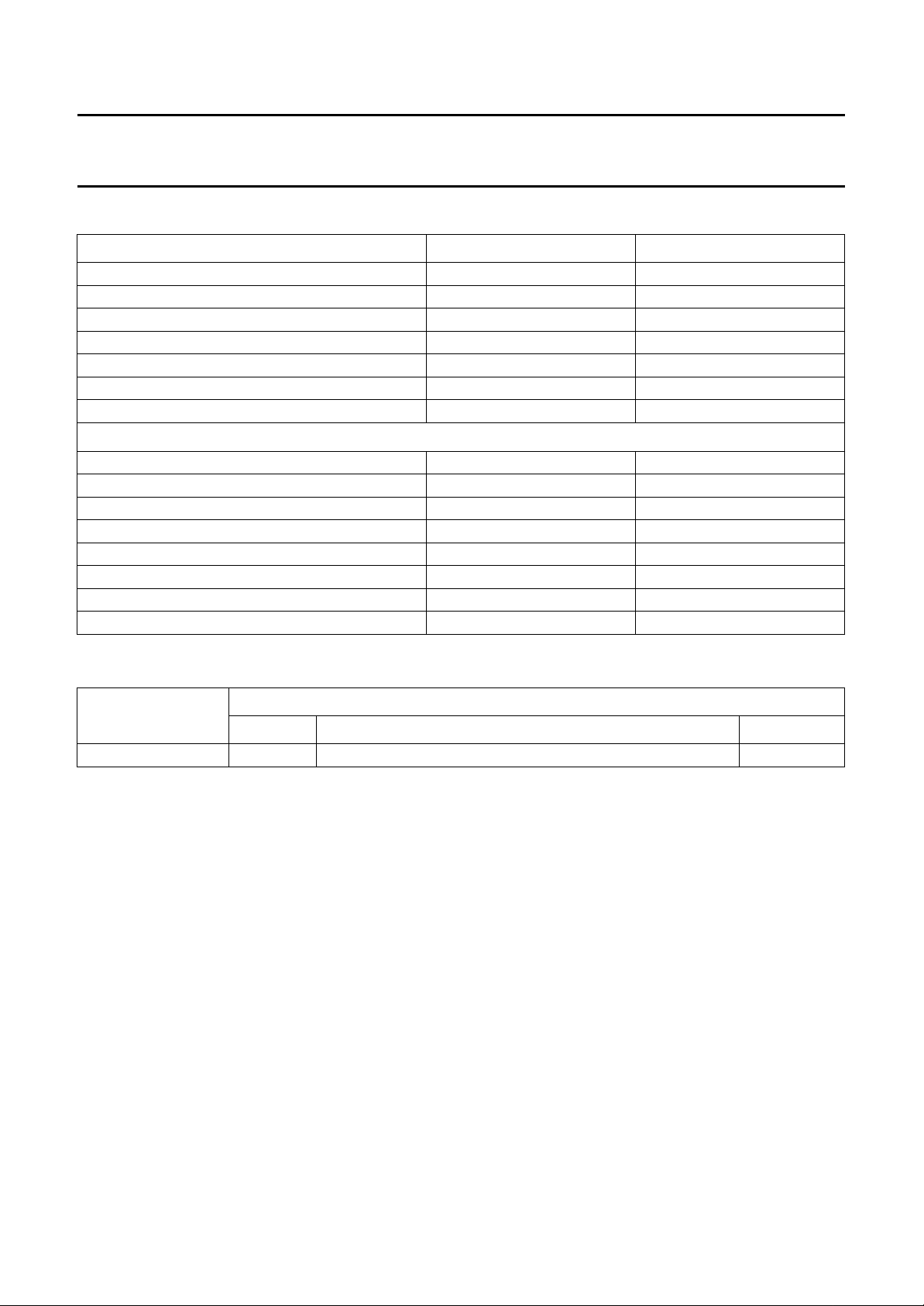
The PCE84C882 is a member of the 84CXXX CMOS
microcontroller family. It is suitable for use with auto-sync
monitors handling mode detection, digital and DPMS
control and has an enhanced OSD facility for menu driving
applications. The device uses the PCE84CXX processor
core and has 8 kbytes of ROM and 192 bytes of RAM. I/O
requirements are catered for with 12 general purpose
bidirectional I/O lines plus 14 derivative I/O lines. 8 PWM
analog outputs are available for analog control purposes
and one 4-bit ADC. The device has an 8-bit counter, for
use in pulse counting applications; an 8-bit timer/counter
with programmable clock and an on-chip programmable
PLL oscillator that generates the OSD clock. A
master-slave I
are also available. The block diagram of the PCE84C882
is shown in Fig.1.
2
C-bus interface and 2 directly testable lines
1996 Jan 08 3
Page 4
Philips Semiconductors Preliminary specification
Microcontroller for monitor OSD
PCE84C882
and auto-sync applications
Table 1 Differences between the PCE84C882 and the PCE84C886
FEATURE PCE84C882 PCE84C886
Maximum dot frequency (f
Maximum Hsync frequency 90 kHz 64 kHz
PLL prescaler value 2 or 4 2
Digital to Analogue Converter 1channel 3 channels
Pulse Width Modulated outputs 8 channels 9 channels
Derivative I/O pins 14 16
Counter T3 input edge sensitivity 0.4 µs1µs
Pin assignment
Pin 21 V
Pin 22 C DP07/PWM7
Pin 23 V
Pin 24 DP05 DP05/PWM5
Pin 30 V
Pin 37 DP07/PWM7 DP11/ADC1
Pin 38 DP06/PWM6 DP10/ADC0
Pin 41 TEST/EMU C
) 20 MHz 14 MHz
OSD
SSP
DDP
SS
V
SS
DP06/PWM6
TEST/EMU
3 ORDERING INFORMATION
TYPE NUMBER
NAME DESCRIPTION VERSION
PCE84C882 SDIP42 plastic shrink dual in-line package; 42 leads (600 mil) SOT270-1
PACKAGE
1996 Jan 08 4
Page 5
Philips Semiconductors Preliminary specification
Microcontroller for monitor OSD
and auto-sync applications
4 BLOCK DIAGRAM
handbook, full pagewidth
INTN / T0 T3
CPU
V
DD
XTAL1 (IN)
XTAL2 (OUT)
T1
8-BIT
TIMER /
EVENT
COUNTER
8-BIT
COUNTER
ROM
8 kbytes
RAM
192 bytes
V
SSP
V
OSCILLATOR
C
DDP
PLL
ON SCREEN DISPLAY
PCE84C882
FB
VOW0 VOW2
VSYNCN
VOW1
(3)(3)
8-bit internal bus
HSYNCN
RESET
PARALLEL
I / O
TEST / EMU
V
SS
(1) Alternative function of DP0.
(2) Alternative function of DP1.
(3) Alternative function of DP2.
PORTS
8
P0
P1
PCF84CXX
core
excluding
ROM / RAM
4
8-BIT
I / O
PORTS
28 4
DP0 DP1 DP2
Fig.1 Block diagram.
3 x 6-BIT PWM
4 x 7-BIT PWM
(1) (2) (2) (3)
PWM0
to
PWM7
2
14-BIT
PWM
PWM8 ADC2 SDA SCL
4-BIT ADC
I C-BUS
INTERFACE
MGC708
(3)
1996 Jan 08 5
Page 6
Philips Semiconductors Preliminary specification
Microcontroller for monitor OSD
and auto-sync applications
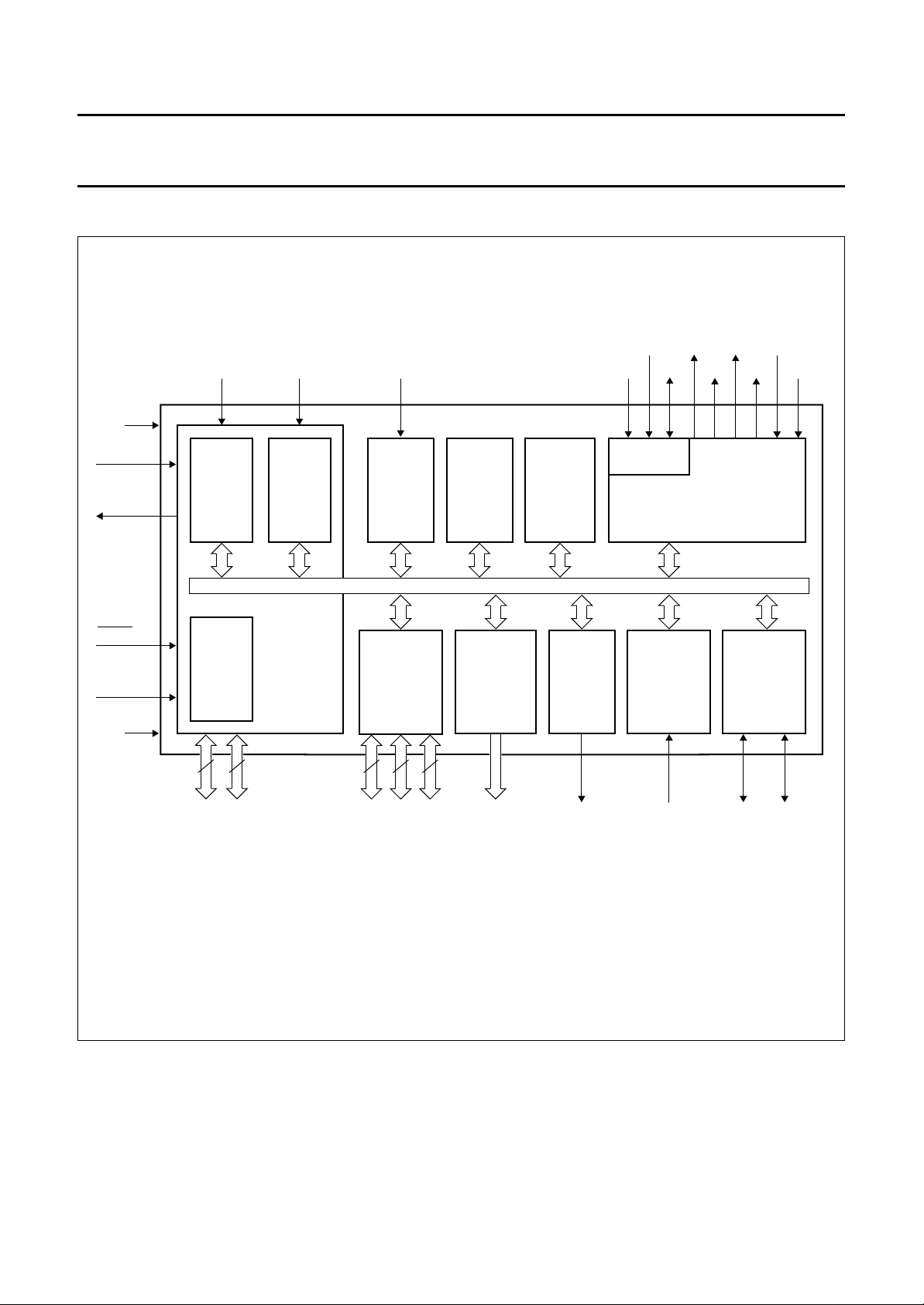
5 PINNING INFORMATION
5.1 Pinning
handbook, halfpage
VOW1/DP22
VOW0/DP23
VSYNCN
HSYNCN
DP13/PWM8
FB
VOW2
P10
P11
P12
T3
P14
P00
P01
P02
P03
P04
P05
P06
P07
V
SSP
1
2
3
4
5
6
7
8
9
10
11
12
13
14
15
16
17
18
19
20
21
PCE84C882
MGC709
V
42
DD
41
TEST/EMU
40
DP20/SDA
39
DP21/SCL
38
DP06/PWM6
37
DP07/PWM7
36
DP12/ADC2
35
INTN/T0
34
T1
33
RESET
32
XTAL2 (OUT)
31
XTAL1 (IN)
30
V
SS
29
DP00/PWM0
28
DP01/PWM1
27
DP02/PWM2
26
DP03/PWM3
25
DP04/PWM4
24
DP05
23
V
DDP
22
C
PCE84C882
Fig.2 Pin configuration.
1996 Jan 08 6
Page 7

Philips Semiconductors Preliminary specification
Microcontroller for monitor OSD
PCE84C882
and auto-sync applications
5.2 Pin description
Table 2 SDIP42 package
SYMBOL PIN DESCRIPTION
FB 1 Video Fast Blanking output.
VOW2 2 Video character output VOW2.
VOW1/DP22 3 Video character output VOW1 or Derivative Port line DP22.
VOW0/DP23 4 Video character output VOW0 or Derivative Port line DP23.
VSYNCN 5 Vertical synchronization signal input.
HSYNCN 6 Horizontal synchronization signal input.
P10 7 Port line 10 or emulation input
P11 8 Port line 11 or emulation input
DP13/PWM8 9 Derivative I/O port or PWM8 output.
P12 10 Port line 12 or emulation input DXALE.
T3 11 Secondary 8-bit counter input (Schmitt trigger).
P14 12 Port line 14 or emulation output DXINT.
P00 to P07 13 to 20 General I/O port lines.
V
SSP
21 Ground pin of PLL circuit.
C 22 External low-pass filter for on-chip PLL OSD oscillator.
V
DDP
DP00/PWM0 to DP07/PWM7 29, 28, 27, 26,
V
SS
23 Power supply pin of PLL circuit.
Derivative I/O ports or PWM outputs. Note that DP05 has no
25, 24, 38, 37
derivative function.
30 Ground pin.
XTAL1 (IN) 31 Oscillator input pin for system clock.
XTAL2 (OUT) 32 Oscillator output pin for system clock.
RESET 33 Reset input; active LOW input initializes device.
T1 34 Direct testable pin or event counter input.
INTN/T0 35 External interrupt or direct testable pin.
DP12/ADC2 36 Derivative I/O port or ADC Channel 2 input.
2
DP21/SCL 39 Derivative port line or I
DP20/SDA 40 Derivative port line or I
C-bus clock input.
2
C-bus data input.
TEST/EMU 41 Control input for testing and emulation mode, normally LOW.
V
DD
42 Power supply.
DXWR.
DXRD.
1996 Jan 08 7
Page 8
Philips Semiconductors Preliminary specification
Microcontroller for monitor OSD
and auto-sync applications
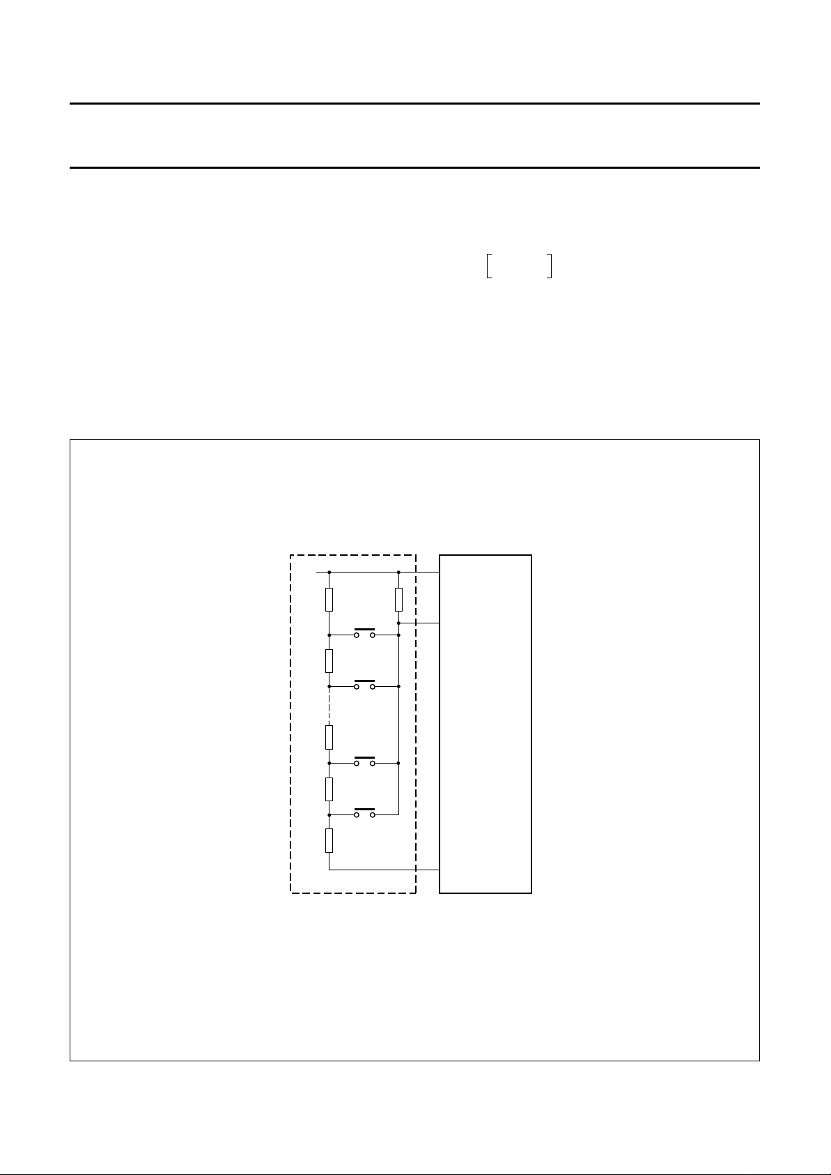
6 RESET
The RESET pin may be used as an active LOW input to
initialize the microcontroller to a defined state.
An active reset can be generated by driving theRESET pin
from an external logic device. Such an active reset pulse
should not fall off before VDD has reached its
f
-dependent minimum operating voltage.
xtal
A Power-on-reset can be generated using an external RC
circuit. To avoid overload of the internal diode, an external
diode should be added in parallel if C
RC circuit is shown in Fig.3.
6.1 Reset trip level
The RESET trip voltage level for the PCE84C882 is in the
range 0.7 to 1.9 V.
If any input (for example Hsync) goes HIGH before V
applied, latch-up may occur and in this situation the
PCE84C882 cannot be reset. The cause and effect of
latch-up is shown in Fig.4.
6.2 Reset status
RESET
≥ 2.2 µF. The
is
DD
handbook, halfpage
V
DD
R
RESET
( 100 kΩ)
RESET
C
RESET
V
SS
PCA84C8XX
Fig.3 External components for RESET pin.
handbook, halfpage
V
DD
V
DD
PCE84C882
internal reset
MLC259
internal V
DD
• Derivative Registers reset status; see Table 38 for
details
• Program Counter 00H
• Memory Bank 0
• Register Bank 0
• Stack Pointer 00H
• All interrupts disabled
• Timer/event counter 1 stopped and cleared
• Timer pre-scaler modulo-32 (PS = 0)
• Timer flag cleared
• Serial I/O interface disabled (ESO = 0) and in slave
receiver mode
• Idle and Stop mode cleared.
Hsync
R
RESET
C
RESET
V
SS
HSYNCN
V
SS
RESET
PCE84C882
internal reset
MGC710
Fig.4 The influence of an active HIGH signal being
applied before Power-on-reset.
1996 Jan 08 8
Page 9
Philips Semiconductors Preliminary specification
Microcontroller for monitor OSD
and auto-sync applications
7 ANALOG (DC) CONTROL
The PCE84C882 has eight Pulse Width Modulated (PWM)
outputs for analog control purposes e.g. brightness,
contrast, H-shift, V-shift, H-width, V-size, E-W, R (or G or
B) gain control etc. Each PWM output generates a pulse
pattern with a programmable duty cycle.
The eight PWM outputs are specified below:
• 3 PWM outputs with 6-bit resolution (PWM4, 6 and 7)
• 4 PWM outputs with 7-bit resolution (PWM0 to PWM3)
• 1 PWM output with 14-bit resolution (PWM8).
The 6 and 7-bit PWM outputs are described in Section 7.1;
the 14-bit PWM output is described in Section 7.2 and a
typical PWM output application is described in Section 7.3.
7.1 6 and 7-bit PWM outputs
PWM outputs PWM0 to PWM4, PWM6 and PWM7, share
the same pins as Derivative Port lines DP00 to DP04,
DP06 and DP07, respectively. Selection of the pin function
as either a PWM output or a Derivative Port line is
achieved using the appropriate PWMnE bit in Register 21
(see Table 38).
PCE84C882
The duty cycle of each PWM output is dependent upon the
programmable contents of its associated data latch
(Registers 10 to 17 respectively, Register 15 is not used
as there is no PWM5 output). As the clock frequency of
each PWM circuit is
generated can be calculated as shown below.
Pulse width
=
Where (PWMn) is the decimal value held in the data latch.
The maximum repetition frequency (f
7-bit PWM outputs is shown below.
For the 6-bit PWM outputs:
For the 7-bit PWM outputs:
The block diagram for the 6 and 7-bit PWM outputs is
shown in Fig.5.
1
⁄3× f
xtal
3 PWMn()×
---------------------------------f
xtal
, the pulse width of the pulse
) of the 6 and
PWM
f
xtal
=
f
PWM
f
PWM
--------- 192
f
xtal
=
--------- 384
The polarity of the PWM outputs is programmable and is
selected by the P7LVL or the P6LVL bit in Register 23
(see Section 12.2). The state of the P7LVL bit determines
the polarity of the 7-bit PWMs; the state of the P6LVL bit
determines the polarity of the 6-bit PWMs.
handbook, full pagewidth
f
xtal
3
6 or 7-BIT PWM DATA LATCH
6 or 7-BIT DAC PWM
CONTROLLER
internal data bus
Q
Q
P6LVL/P7LVL
DP0x data
I/O
PWMnE
DP0x/PWMx
MLC069
Fig.5 Block diagram for 6 and 7-bit PWMs.
1996 Jan 08 9
Page 10
Philips Semiconductors Preliminary specification
Microcontroller for monitor OSD
and auto-sync applications
f
handbook, full pagewidth
xtal
3
64
or
128
00
01
m
63
or
127
1 2 3 m m + 1 m + 2
decimal value PWM data latch
PCE84C882
64
or
128
1
MLC261
Fig.6 Typical non-inverted output pulse patterns for 6 or 7-bit PWM outputs.
1996 Jan 08 10
Page 11
Philips Semiconductors Preliminary specification
Microcontroller for monitor OSD
and auto-sync applications
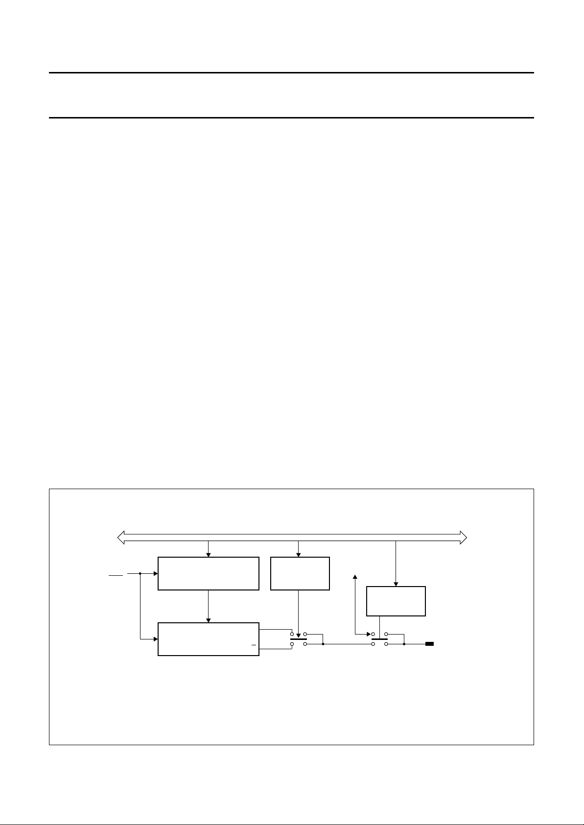
7.2 14-bit PWM output
PWM8 shares the same pin as Derivative Port line DP13.
Selection of the pin function as either a PWM output or as
a Derivative Port line is achieved using the PWM8E bit in
Register 22 (see Section 12.1).
The block diagram for the 14-bit PWM output is shown in
Fig.7 and comprises:
• Two 7-bit latches: PWM8L (Register 18) and PWM8H
(Register 19)
• 14-bit data latch (PWMREG)
• 14-bit counter
• Coarse pulse controller
• Fine pulse controller
• Mixer.
Data is loaded into the 14-bit data latch (PWMREG) from
the two 7-bit data latches (PWM8H and PWM8L) when
either of these data latches is written to. The upper seven
bits of PWMREG are used by the coarse pulse controller
and determine the coarse pulse width; the lower seven bits
are used by the fine pulse controller and determine in
which subperiods fine pulses will be added. The outputs
OUT1 and OUT2 of the coarse and fine pulse controllers
are ‘ORED’ in the mixer to give the PWM8 output. The
polarity of the PWM8 output is programmable and is
selected by the P8LVL bit in Register 23, this is described
in Section 12.2.
PCE84C882
7.2.1 C
An active HIGH pulse is generated in every subperiod; the
pulse width being determined by the contents of PWM8H.
The coarse output (OUT1) is LOW at the start of each
subperiod and will remain LOW until the time
3f
⁄ PWM8H 1+()×[]
then go HIGH and remain HIGH until the start of the next
subperiod. The coarse pulse width may be calculated as
shown below.
Pulse duration 127 PWM8H–()
7.2.2 F
Fine adjustment is achieved by generating an additional
pulse in specific subperiods. The pulse is added at the
start of the selected subperiod and has a pulse width of
3/f
xtal
subperiods a fine pulse will be added. It is the logic 0 state
of the value held in PWM8L that actually selects the
subperiods. When more than one bit is a logic 0 then the
subperiods selected will be a combination of those
subperiods specified in Table 3. For example, if
PWM8L = 111 1010 then this is a combination of:
• PWM8L = 111 1110: subperiod 64 and
• PWM8L = 111 1011: subperiods 16, 48, 80 and 112.
Pulses will be added in subperiods 16, 48, 64, 80 and 112.
This example is illustrated in Fig.10.
OARSE ADJUSTMENT
xtal
INE ADJUSTMENT
has elapsed. The output will
3
×=
-------f
xtal
. The contents of PWM8L determine in which
As the 14-bit counter is clocked by1⁄3× f
, the repetition
xtal
times of the coarse and fine pulse controllers may be
calculated as shown below.
384
r
t
sub
=
=
49152
---------------f
xtal
--------- f
xtal
Coarse controller repetition time:
Fine controller repetition time:
t
Figure 8 shows typical PWM8 outputs, with coarse
adjustment only, for different values held in PWM8H.
Figure 9 shows typical PWM8 outputs, with coarse and
fine adjustment, after the coarse and fine pulse controller
outputs have been ‘ORED’ by the mixer.
1996 Jan 08 11
When PWM8L holds 111 1111 fine adjustment is inhibited
and the PWM8 output is determined only by the contents
of PWM8H.
Table 3 Additional pulse distribution
PWM8L ADDITIONAL PULSE IN SUBPERIOD
111 1110 64
111 1101 32 and 96
111 1011 16, 48, 80 and 112
111 0111 8, 24, 40, 56, 72, 88, 104 and 120
110 1111 4, 12, 20, 28, 36, 44, 52...116 and 124
101 1111 2, 6, 10, 14, 18, 22, 26, 30...122 and 126
011 1111 1, 3, 5, 7, 9, 11, 13, 15, 17...125 and 127
Page 12
Philips Semiconductors Preliminary specification
Microcontroller for monitor OSD
and auto-sync applications
handbook, full pagewidth
‘MOVE instruction’
PWM8H
DATA LOAD
TIMING PULSE
LOAD
Internal data bus
7 7
PWMREG
PWM8L
PCE84C882
‘MOV instruction’
polarity
control bit
P8LVL
7 7
COARSE 7-BIT
PWM
MIXER
Q
Q14 to 8 Q7 to 1
14-BIT COUNTER
FINE PULSE
GENERATOR
OUT2OUT1
Q
MLC071
PWM8 output
f = f
tdac xtal
3
Fig.7 14-bit PWM Block diagram.
1996 Jan 08 12
Page 13
Philips Semiconductors Preliminary specification
Microcontroller for monitor OSD
and auto-sync applications
f
handbook, full pagewidth
xtal
3
127 0 1 2 m m + 1 m + 2
00
01
m
127
decimal value PWM8H data latch
PCE84C882
127 0 1
MLC263
f
xtal
handbook, full pagewidth
3
127 0 1 2 m m + 1 m + 2
00
01
m
127
Fig.8 Non-inverted PWM8 output patterns - Coarse adjustment only.
127 0 1
MLC262
decimal value PWM8H data latch
Fig.9 Non-inverted PWM8 output patterns - Coarse and Fine adjustment.
1996 Jan 08 13
Page 14
Philips Semiconductors Preliminary specification
Microcontroller for monitor OSD
and auto-sync applications
handbook, full pagewidth
111 1110
111 1011
111 1010
PWM8L
t
sub0
t
sub16
t
sub32
t
sub48
t
t
sub64
PCE84C882
r
t
sub80
t
sub96
t
sub112
t
sub127
MLC755
Fig.10 Fine adjustment output (OUT2).
7.3 A typical PWM output application
A typical PWM application is shown in Fig.11. The buffer is
used to reduce jitter on the OSD. R1 and C1 form the
integration network the time constant of which should be at
least 5 times greater than the repetition period of the PWM
output pattern. In order to smooth a changing PWM output
a high value of C1 should be chosen. The value of C1 will
normally be in the range 1 to 10 µF. The potential divider
chain formed by R2 and R3 is used only when the output
voltage is to be offset. The output voltages for this
application are calculated using Equations (1) and (2).
R3 supply voltage×
=
V
V
min
----------------------------------------------------
max
R1 R3×
--------------------- R1 R3+
=
-------------------------------------------------------------------
R3
R2
R1 R2×
+
---------------------R1 R2+
supply voltage×
R1 R3×
+
---------------------R1 R3+
(1)
(2)
The loop from the PWM pin through R1 and C1 to VSS will
radiate high frequency energy pulses. In order to limit the
effect of this unwanted radiation source, the loop should
be kept short and a high value of R1 selected. The value
of R1 will normally be in the range 3.3 to 100 kΩ. It is good
practice to avoid sharing VSS (pin 30) with the return leads
of other sensitive signals.
handbook, halfpage
PCE84C882
Fig.11 Typical PWM output circuit.
PWMn
V
SS
MGC711
R1
R2
C1 R3
supply
voltage
analog
output
1996 Jan 08 14
Page 15

Philips Semiconductors Preliminary specification
Microcontroller for monitor OSD
and auto-sync applications
8 ANALOG-TO-DIGITAL CONVERTER (ADC)
The single channel ADC comprises a 4-bit
Digital-to-Analog Converter (DAC); a comparator; an
analog channel selector and control circuitry. As the digital
input to the 4-bit DAC is loaded by software (a subroutine
in the program), it is known as a software ADC. The block
diagram is shown in Fig.12.
The ADC input ADC2, shares the same pin as Derivative
Port line DP12. Selection of the pin function as either an
ADC input or as a Derivative Port line is achieved using bit
ADCE2 in Register 22. When ADCE2 = 1, the ADC
function is enabled (see Section 12.1).
The ADC channel selector is controlled by the ADCS1 and
ADCS0 bits in Register 20. As the PCE84C882 provides
only one ADC channel, ADCS1 bit must be set to a logic 1
and ADCS0 bit must be set to a logic 0. All other settings
are invalid.
The 4-bit DAC analog output voltage (V
by the decimal value of the data held in bits DAC0 to DAC3
of Register 20. V
and Table 4 lists the V
is calculated as shown in Equation (3)
ref
values assuming VDD=5V.
ref
V
DD
V
----------
ref
16
DAC value 1+()×=
When the analog input voltage is higher than V
COMP bit in Register 20 will be HIGH.
Table 4 Selection of V
ref
DAC3 DAC2 DAC1 DAC0 V
00000.3125
00010.6250
00100.9375
00111.2500
01001.5625
01011.8750
01102.1875
01112.5000
10002.8125
10013.1250
10103.4375
10113.7500
11004.0625
11014.3750
11104.6875
11115.0000
) is determined
ref
, the
ref
ref
(3)
(V)
PCE84C882
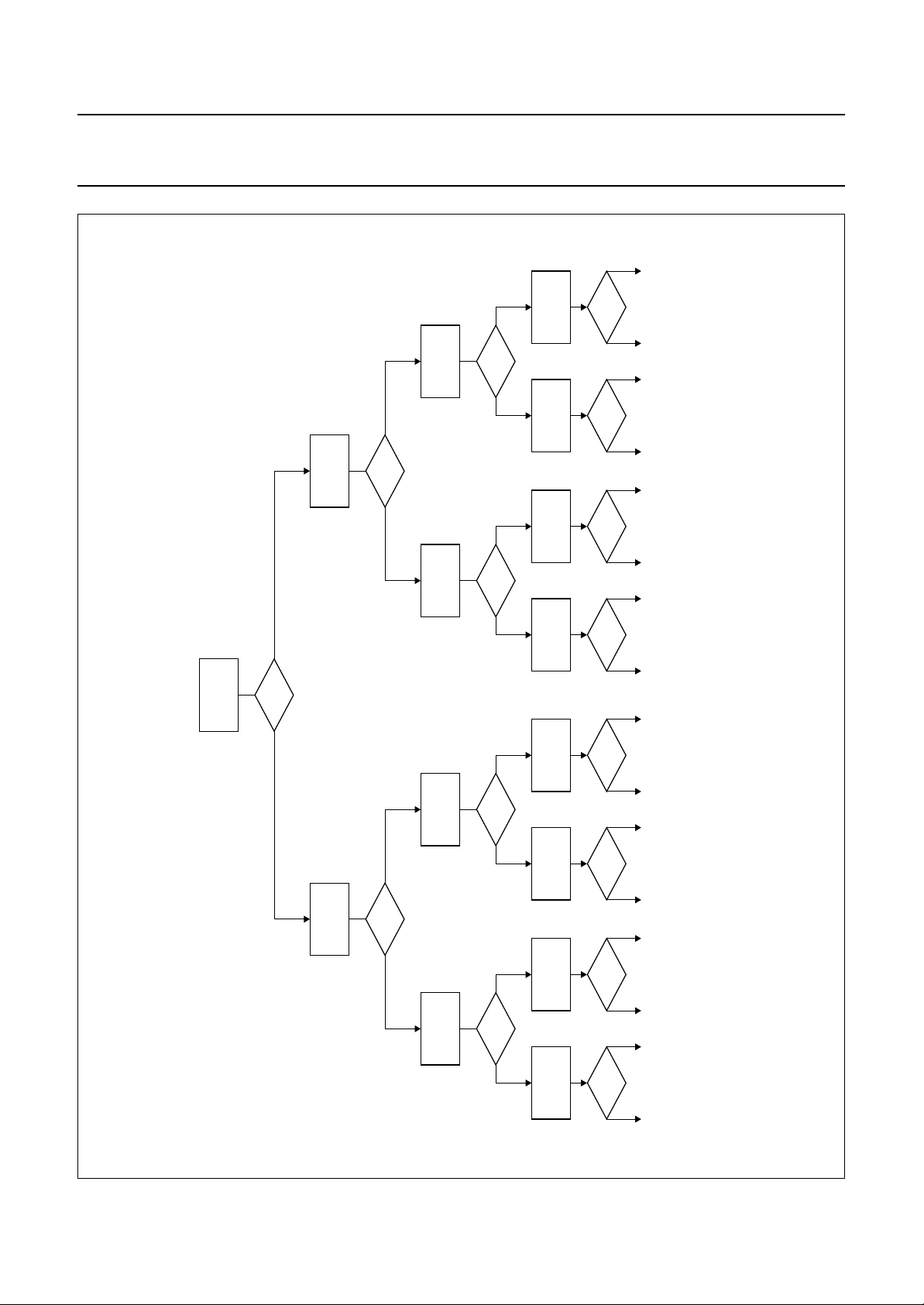
8.1 Conversion algorithm
There are many algorithms available to achieve the ADC
conversion. The algorithm described below and shown in
Fig.13 uses an iteration process.
1. Enable and then select the ADC2 channel for
conversion. Channel selection is achieved using bits
ADCS1 and ADCS0 in Register 20.
2. Set the digital input to the DAC to 1000. The digital
input to the DAC is selected using bits DAC3 to DAC0
in Register 20.
3. Determine the result of the compare operation. This is
achieved by reading the COMP bit in Register 20
using the instruction MOV A, D20. If COMP = 1; the
analog input voltage is higher than the reference
voltage (V
lower than the reference voltage (V
4. If COMP = 1; then the analog input voltage is higher
than the reference voltage (V
digital input to the DAC needs to be increased. Set the
input to the DAC to 1100.
5. If COMP = 0; then the analog input voltage is lower
than the reference voltage (V
digital input to the DAC needs to be decreased. Set the
input to the DAC to 0100.
6. Determine the result of the compare operation by
reading the COMP bit in Register 20.
7. For the DAC = 1100 case
If COMP = 1; then the analog input voltage is still
greater than V
DAC needs to be increased again. Set the input to the
DAC to 1110.
If COMP = 0; then the analog input voltage is now less
than V
needs to be decreased. Set the input to the DAC to
1010
8. For the DAC = 0100 case
If COMP = 1; then the analog input voltage is now
greater than V
DAC needs to be increased. Set the input to the DAC
to 0110.
If COMP = 0; then the analog input voltage is still lower
than V
needs to be decreased again. Set the input to the DAC
to 0010.
). If COMP = 0; the analog input voltage is
ref
).
ref
) and therefore the
ref
) and therefore the
ref
and therefore the digital input to the
ref
and therefore the digital input to the DAC
ref
and therefore the digital input to the
ref
and therefore the digital input to the DAC
ref
1996 Jan 08 15
Page 16
Philips Semiconductors Preliminary specification
Microcontroller for monitor OSD
and auto-sync applications
9. The operations detailed in 6, 7 and 8 above are
repeated and each time the digital input to the DAC is
changed accordingly; as dictated by the state of the
COMP bit. The complete process is shown in Fig.13.
Each time the DAC input is changed the number of
values which the analog input can take is reduced by
half. In this manner the actual analog value is honed
into. The value of the analog input (VA) is determined
using Equation (4):
V
V
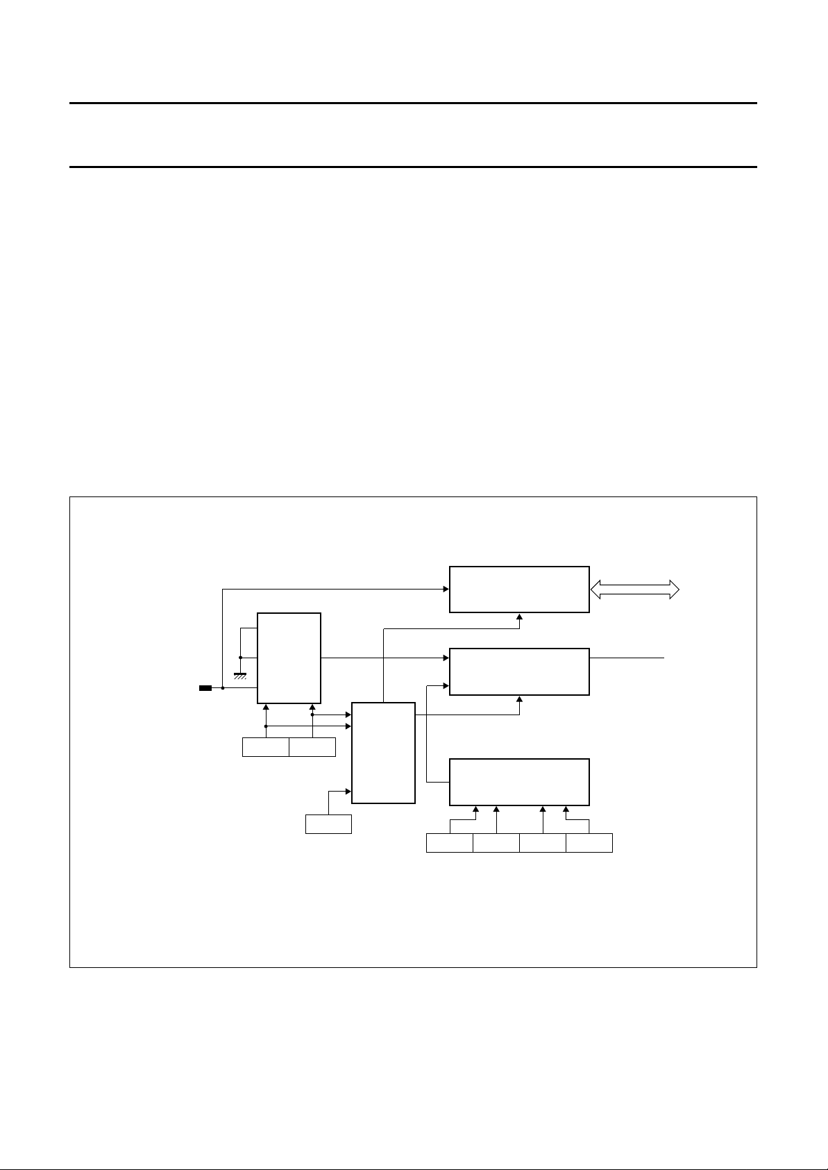
As the conversion time of each compare operation is
greater than 6 µs but less than 9 µs; a NOP instruction is
recommended to be used in between the instructions that
change the value of V
the COMP bit.
DD
----------
A
DAC value 1+()×=
16
; select the ADC channel and read
ref
(4)
PCE84C882
andbook, full pagewidth
DP12/ADC2
Channel selection
ADC
CHANNEL
SELECTOR
ADCS1 ADCS0
ADCE2
ADC enable selection
Fig.12 Block diagram of 1 channel ADC.
ENABLE
SELECTOR
V
ref
+
−
DAC3
DERIVATIVE PORT
SELECTOR
EN2
COMPARATOR
EN
4-BIT DAC
DAC2 DAC1 DAC0
DAC value selection
Internal bus
COMP bit
‘MOV A, D20’
instruction
to read COMP bit
MGC712
1996 Jan 08 16
Page 17
Philips Semiconductors Preliminary specification
Microcontroller for monitor OSD
and auto-sync applications
Value = 0100
COMP = 1
TF
Value = 0010
COMP = 1
TF
Value = 0001
Value = 0011
Value = 0101
PCE84C882
0000
MLC073
COMP = 1
TF
00010011
0010
COMP = 1
TF
COMP = 1
TF
0101 0100
Value = 1000
TF
COMP = 1
Value = 1100
TF
COMP = 1
Value =0110
Value = 1010
Value = 1110
COMP = 1
TF
COMP = 1
TF
COMP = 1
TF
Value = 0111
Value = 1001
Value = 1011
Value = 1101
COMP = 1
TF
0111 0110
COMP = 1
TF
1001 10001011
1010
COMP = 1
TF
COMP = 1
TF
1101 1100
handbook, full pagewidth
Fig.13 Example of converting algorithm for software ADC.
1996 Jan 08 17
Value = 1111
COMP = 1
TF
1111 1110
Page 18
Philips Semiconductors Preliminary specification
Microcontroller for monitor OSD
and auto-sync applications
8.2 Typical ADC application
The ADC2 channel of the PCE84C882 can be used in
keypad applications to detect and identify the operation of
individual keys. The circuit for a 14-key application is
shown in Fig.14.
When no key is depressed the input voltage at the
DP12/ADC2 pin will be greater than15⁄16× VDD and if the
DAC value selected is 1110 then the COMP bit will be
HIGH. When any key is depressed the input voltage at the
DP12/ADC2 pin will change, and as each key will generate
its own unique input voltage, this can be measured by the
ADC2 channel and the actual key depressed can then be
identified.
PCE84C882
The input voltage generated by the operation of any key
(ignoring the effect of the 100 kΩ resistor) can be
calculated as follows:
V
ADCn
n 0.5–()
-----------------------16
Where n is the key number and can take any integer value
in the range 1 to 14.
The input voltage at the ADC input will be influenced by the
tolerance of the resistors and the length of the cable
connecting the keypad to the monitor. In the worse case
situation this may reduce the number of keys that can be
uniquely detected and identified.
V
×=
DD
handbook, halfpage
5 kΩ
2 kΩ
2 kΩ
2 kΩ
1 kΩ
100 kΩ
key 14
key 13
key 2
key 1
14 key matrix
V
DD
DP12/ADC2
PCE84C882
V
SS
MGC718
Fig.14 A typical ADC application for keypad detection.
1996 Jan 08 18
Page 19

Philips Semiconductors Preliminary specification
Microcontroller for monitor OSD
and auto-sync applications
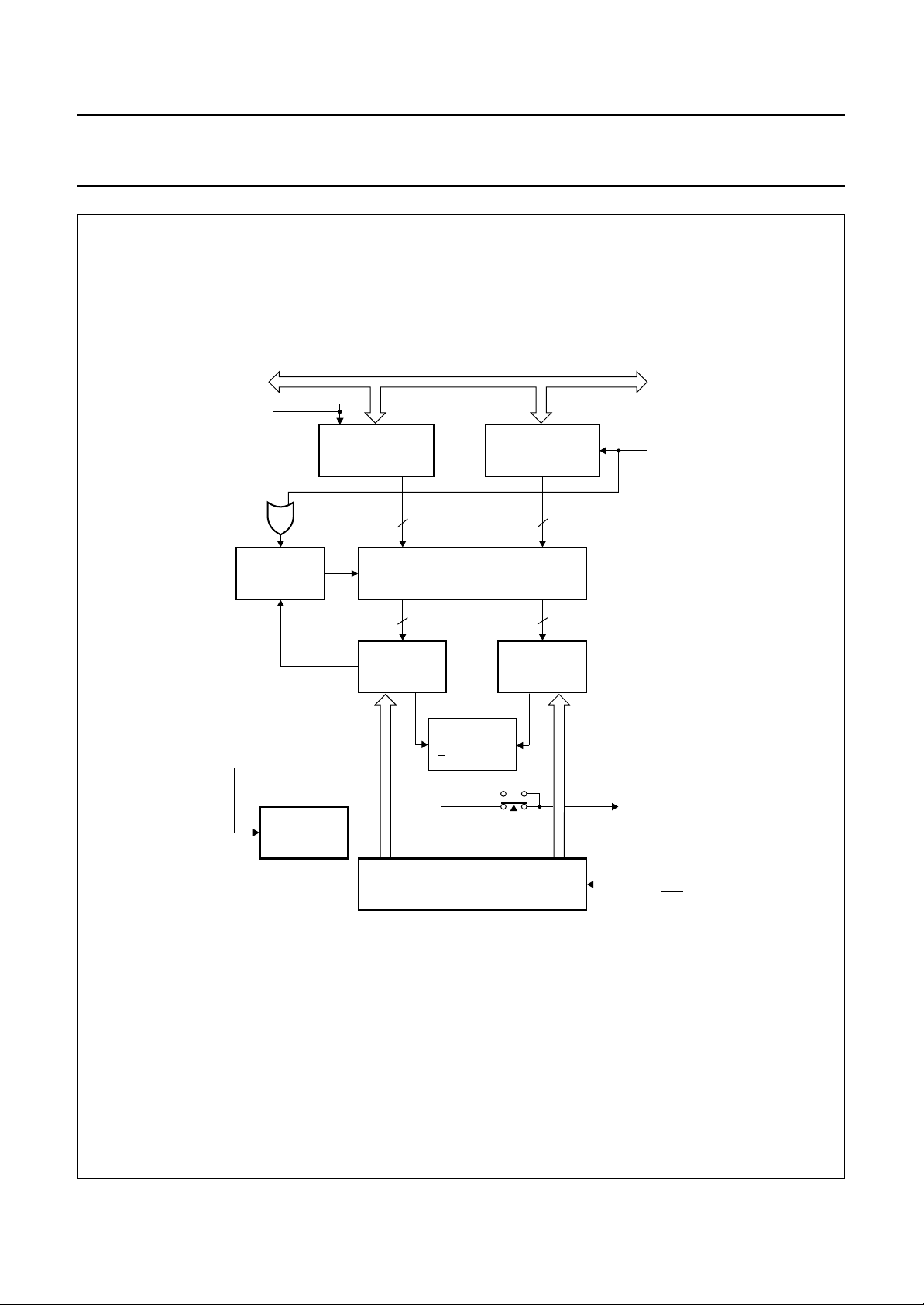
9 ON SCREEN DISPLAY (OSD)
The OSD feature of the PCE84C882 enables the user to
display information on the monitor screen. Display
information can be created using 62 customer designed
characters, a space character and a carriage return code.
The OSD block diagram is shown in Fig.15.
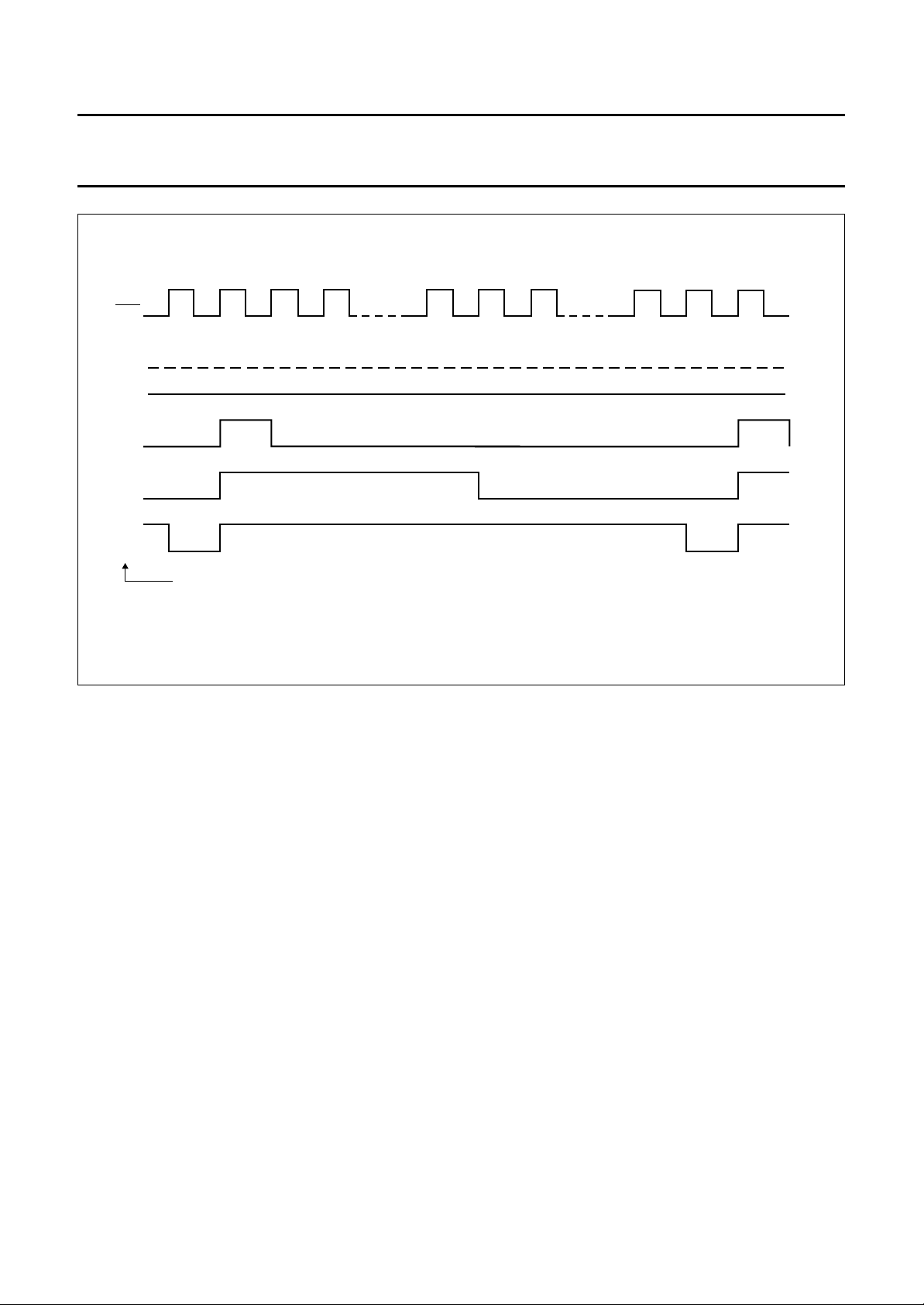
9.1 Horizontal starting position control
The horizontal starting position counter is incremented
every OSD clock after Hsync becomes inactive and is
reset when Hsync becomes active. The horizontal starting
position of the display row is determined by the contents of
Register 36; 1 of 64 positions may be selected as
explained in Section 12.6.
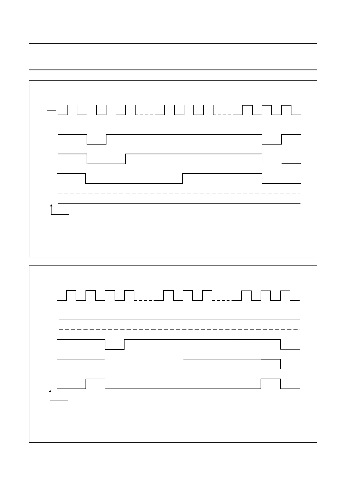
The polarity of the active state of the HSYNCN input is
programmable and is determined by the Hp bit in
Register 34; see Section 12.4. The active HIGH and active
LOW states as selected by the Hp bit are shown in Fig.16.
9.2 Vertical starting position control
The vertical starting position counter is incremented every
Hsync cycle and is reset when Vsync becomes active. The
vertical starting position of the display row is determined by
the contents of Register 35; 1 of 64 positions may be
selected as explained in Section 12.5.
To achieve the same starting position with different display
resolutions, only the contents of Register 35 need to be
changed, the contents of Register 36 remain the same.
The lowest vertical starting position that can be selected,
is located on the 256th scan-line. However, lower positions
may be achieved using the Carriage Return Code.
When the selected horizontal and vertical starting
positions are reached on screen; the OSD is enabled. The
character selected in display RAM is then displayed.
The polarity of the active state of the VSYNCN input is
programmable and is determined by the Vp bit in Register
34; see Section 12.4. The active HIGH and active LOW
states as selected by the Vp bit are shown in Fig.16.
9.3 Vertical jumping cancelling
If the H-shift of the monitor is altered then vertical jumping
of the OSD may occur if the rising or falling edges of the
Hsync and Vsync signals are too close. The PCE84C882
has on-chip vertical cancelling circuitry that prevents this
from happening.
PCE84C882
9.4 On-chip clock generator
The on-chip oscillator generates an OSD clock that is
auto-sync with Hsync. The frequency of the OSD clock is
programmable and is determined by the contents of the
7-bit counter (Register 25) and also the prescaler value
selected by mask option (a prescaler value of 2 or 4 can be
selected). For 31 to 64 kHz auto-sync monitors, a
prescaler value of 4 is selected; for 31 to 90 kHz auto-sync
monitors a prescaler value of 2 or 4 can be selected.
The OSD clock frequency is calculated as follows:
f
OSDfHsync
Where (Register 25) denotes the decimal value held in
Register 25.
The block diagram of the OSD clock is shown in Fig.17.
The internal reference frequency is connected to Hsync,
and if the frequency of Hsync changes the output
frequency (f
Hsync signal is designed active HIGH, consequently f
synchronized with the falling edge of this signal (end of
back-tracing period).
The OSD clock is enabled/disabled by the state of the EN
bit in Register 34; see Section 12.4. When the OSD clock
is disabled the oscillator remains active, therefore the
transient time from the OSD clock start-up to locking into
the external Hsync signal is reduced. To ensure that the
OSD clock is stable and in-phase with Hsync before the
display is enabled, the End bit of the Space Code can be
used to enable the OSD feature; the procedure is as
follows.
1. Write a Space Code to address 00H of display RAM,
the End bit value is logic 1.
2. Set the EN bit in Register 34 to logic 0.
3. Write a Space Code to address 00H of display RAM,
the End bit value is logic 0.
Two dedicated power pins: V
oscillator supplies from other circuits thus reducing any
radiated noise that might effect the Voltage Controlled
Oscillator. Radiated noise is further reduced because as
the oscillator is always active after power-on when the
OSD clock is enabled no large currents will flow (as in the
case of RC or LC oscillators).
2or4()Register 25()××=
) will be changed linearly. The internal
OSD
DDP
and V
, isolate the
SSP
PLL
is
1996 Jan 08 19
Page 20

Philips Semiconductors Preliminary specification
Microcontroller for monitor OSD
and auto-sync applications
CONTROL
REGISTER
RAM
DISPLAY
CHARACTER
BUFFER
ADDRESS
SELECTOR
ROM
DISPLAY
AND
OUTPUT STAGE
DISPLAY CONTROL
RGBFB
control
signals
PCE84C882
MGC714
VOW1 VOW0 VOW2 FB
COUNTER
WRITE ADDRESS
POSITION
HORIZONTAL
CONTROL
CHARACTER SIZE
POSITION
VERTICAL
REGISTER/
COUNTER
REGISTER/
PLL
C
COUNTER
CONTROL REGISTER
INSTRUCTION DECODER
OSCILLATOR
CIRCUIT
INTERNAL
SYNCHRONOUS
CONTROL
POLARITY
handbook, full pagewidth
Fig.15 OSD block diagram.
SSP
CPU bus
DDP
V
V
1
R
1996 Jan 08 20
2
1
R
C
VSYNCN
HSYNCN
Page 21

Philips Semiconductors Preliminary specification
Microcontroller for monitor OSD
and auto-sync applications
handbook, full pagewidth
HSYNCN/VSYNCN pin
Hp/Vp = 0 (active LOW)
HSYNCN/VSYNCN pin
Hp/Vp = 1 (active HIGH)
Fig.16 HSYNCN and VSYNCN active level selection.
PCE84C882
character display interval
MLC286
handbook, full pagewidth
Hsync
(30 to 90 kHz)
PHASE/
FREQUENCY
DETECTOR
PROGRAMMABLE
7-BIT COUNTER
CHARGE PUMP
AND
LOOP FILTER
2
mask option
Fig.17 Block diagram for OSD oscillator.
VOLTAGE
CONTROLLED
OSCILLATOR
2
OSD disable
f
PLL
C
f
OSD
MGC716
1996 Jan 08 21
Page 22

Philips Semiconductors Preliminary specification
Microcontroller for monitor OSD
PCE84C882
and auto-sync applications
10 DISPLAY RAM ORGANIZATION
The display RAM is organized as 64 × 10 bits. The general
format of each RAM location is as follows. Bits <9-4> hold
character data (62 customer designed character fonts plus
two reserved codes). Bits <3-0> contain the attributes of
the character font, for example colour, character size,
blinking etc.
Display RAM is updated during the vertical back-tracing
period (Vsync will generate an interrupt when it becomes
active).
Table 5 Format of Character Font Code
987654321 0
C5 C4 C3 C2 C1 C0 T3 T2 T1 T0
Character Font Code (00H - 3DH) Foreground colour Blink
Table 6 Format of Carriage Return Code
9876543210
C5 C4 C3 C2 C1 C0 T3 T2 T1 T0
Carriage Return Code (3EH) Character size Line Spacing
10.1 Description of display RAM codes
There are three data formats for display RAM code:
1. Character Font Code
2. Carriage Return Code
3. Space Code.
The three data formats are shown in Tables 5, 6 and 7.
Table 7 Format of Space Code
987654321 0
C5 C4 C3 C2 C1 C0 T3 T2 T1 T0
Space Code (3FH) Background colour End
1996 Jan 08 22
Page 23

Philips Semiconductors Preliminary specification
Microcontroller for monitor OSD
and auto-sync applications
10.1.1 CHARACTER FONT CODE
If bits <9-4> are in the range (00H to 3DH), then this is a
Character Font Code and 1 from 62 customer designed
character fonts can be selected. Bits <3-1> determine the
colour of the character, a choice of 8 colours being
available. Bit <0> determines whether the character blinks
or not. The blinking duty cycle and frequency are
controlled by Derivative Register 33, see Section 12.3.
The format of the Character Font Code is shown in
Table 5.
Table 8 Selection of Foreground colour
T3
(RED)
0 0 0 black
0 0 1 blue
0 1 0 green
0 1 1 cyan
100red
1 0 1 magenta
1 1 0 yellow
1 1 1 white
Table 9 Selection of Blinking function
T0 BLINKING
10.1.2 C
If bits <9-4> hold 3EH, then this is the Carriage Return
Code. The current display line is terminated (a transparent
pattern appears on the screen) and the next character will
be displayed at the beginning of the next line. Bits <3-2>
select the size of the of the character to be displayed on
the next line. Bits <1-0> determine the spacing between
lines of displayed characters. Spacing is a multiple of the
number of horizontal scan lines. The format of the Carriage
Return Code is shown in Table 6.
ARRIAGE RETURN CODE
T2
(GREEN)
0 OFF
1ON
T1
(BLUE)
COLOUR
PCE84C882
Table 10 Selection of character size
T3 T2 CHARACTER DOT SIZE
0 0 1H/1V
0 1 1H/2V
1 0 1H/3V
1 1 1H/4V
Note
1. H is the OSD clock period; V is the number of
horizontal scan lines per dot.
Table 11 Selection of line spacing
T1 T0 LINE SPACING
0 0 0H line
0 1 4H line
1 0 8H line
1 1 12H line
10.1.3 S
If bits <9-4> hold 3FH, then this is the Space Code. A
transparent pattern, equal to one character width, will be
displayed on the screen. Bits <3-1> determine the
background colour of the characters including the Space
Code in Box shadowing mode, but following the Space
Code in North shadowing mode. See Sections 12.4 and
12.3.1 for more details. Background colour selection is the
same as foreground colour selection. Bit <0> is the
End-of-Display bit and indicates the end of display of the
current screen before exhaustion of display RAM (i.e.
before the 64th RAM location). The format of the Space
Code is shown in Table 7.
Table 12 End of display control
PACE CODE
T0 DISPLAY CONTROL
0 continue display of next character; this
is also the default setting
1 end of display
(1)
1996 Jan 08 23
Page 24

Philips Semiconductors Preliminary specification
Microcontroller for monitor OSD
and auto-sync applications
10.2 Default values of OSD after Power-on-reset
• Frequency of OSD clock: undefined, must be
programmed
• Background/Shadowing mode: No background mode
• Background/Shadowing colour: blue
• Character size: 1H/1V
• OSD disabled
• Full 64 display RAM displayed (End of display bit = 0)
• VOW1E and VOW0E disabled
• Horizontal starting position: 5th dot
• Vertical starting position: 256th scan-line
• Polarity of HSYNCN: active LOW
• Polarity of VSYNCN: active LOW
• Output polarities of FB, VOW0 to VOW2: active HIGH
• Blinking ratio: 3 : 1
• Blinking frequency:1⁄
• Frame background colour: blue.
After a Power-on-reset, the OSD can be set-up as required
by selecting the Space Code as the first character
(address 0) and the Carriage Return Code as the next
character (address 1). This procedure allows the user to
select the initial background colour; character size and
inter-line spacing.
10.3 Loading character data into display RAM
Three Derivative Registers are used to address and load
data into the display RAM. These registers are described
below.
10.3.1 DCR A
This is Derivative Register 30 and holds the address of the
location in display RAM to which the data held in registers
DCRTR and DCRCR will be written to. 1 of 64 locations
can be addressed. Bits 7 and 6 are reserved. The contents
of this register are automatically incremented after each
write operation to a RAM address, and become zero on
overflow.
Table 13 DCR Address Register (DCRAR)
DDRESS REGISTER (DCRAR)
128
× f
Vsync
PCE84C882
10.3.2 DCR ATTRIBUTE REGISTER (DCRTR)
This is Derivative Register 31 and holds the character font
attribute data. The data will be loaded into bits <3-0> of the
location in RAM pointed to by the contents of DCRAR.
Bits 7 to 4 are reserved.
Table 14 DCR Attribute Register (DCRTR)
76543210
−−−−T3 T2 T1 T0
10.3.3 DCR C
This is Derivative Register 32 and holds the character data
that will be loaded into bits <9-4> of the location in RAM
addressed by the contents of DCRAR. Bits 7 and 6 are
reserved.
Table 15 DCR Character Register (DCRCR)
76543210
−−C5 C4 C3 C2 C1 C0
10.4 Writing character data into display RAM
The procedure for writing character data into the display
RAM is as follows:
1. Select the start address in display RAM. The start
address is stored in DCRAR and can take any value
between 0 and 63.
2. Load the character attributes into DCRTR. If the
attributes of a series of displayed characters are the
same, only DCRCR needs to be updated.
3. Load the character data into DCRCR. The character
data will specify either a Character Font Code, the
Carriage Return Code or the Space Code. This
operation loads the selected RAM location with the
data held in registers DCRTR and DCRCR. The
address held in DCRAR is then incremented by ‘1’
pointing to the next RAM location in anticipation of the
next operation.
After a master reset the contents of DCRAR, DCRTR and
DCRCR are zero.
HARACTER REGISTER (DCRCR)
76543210
−−A5 A4 A3 A2 A1 A0
1996 Jan 08 24
Page 25

Philips Semiconductors Preliminary specification
Microcontroller for monitor OSD
and auto-sync applications
11 CHARACTER ROM
64 character fonts may be held in ROM; 62 customer
selected character fonts plus the Carriage Return Code
and the Space Code. Customer selected fonts are mask
programmable. Each character font is stored in a 12 × 19
dot matrix. However, only elements in Rows 1 to 18 can be
selected as visible dots on the screen. Row 0 is only used
for the combination of two characters in a vertical direction
when North shadowing mode is selected.
11.1 Character ROM address map
Figure 18 shows the ROM address map. Addresses 3EH
and 3FH hold the reserved codes for carriage return and
space functions, respectively. Addresses (00H to 3DH)
hold the customer selected character font codes.
11.2 Character ROM organization
ROM is divided into two parts: ROM1 and ROM2. The
organization of the bit patterns stored in ROM 1 and
ROM 2 and also the file format to submit to Philips for
customized character sets is shown in Fig.19. Regarding
Fig.19 the following points should be noted.
PCE84C882
The combination of two cells in a horizontal direction is
straight forward and requires no special precautions to be
taken. When combining character cells in this manner all 4
Background/Shadowing modes are available. An example
of combining two character font cells in a horizontal
direction is shown in Fig.20.
However, the combination of two character font cells in a
vertical direction is more difficult and care must be taken;
otherwise, the new pattern may be created with gaps in its
shadowing. An example of a character pattern with gaps is
shown in Fig.21. Providing the steps listed below are
followed no problems with shadowing will occur.
• The line spacing between two rows of characters must
be programmed to 0H. This procedure is explained in
Section 10.1.2.
• If the North shadowing mode is selected then when
combining two character cells in a vertical direction
Row 0 must contain the same bit pattern as held in
Row 18 of the character directly above it. This is shown
in Fig.22.
• If North shadowing is not required then Row 0 should
contain all zeros.
1. Row 0 of each font is reserved for vertical combination
of two fonts.
2. Binary 1 denotes visual dots.
3. ROM1 and ROM2 data files are in INTEL hex format
on a byte basis. Each byte is structured high nibble
followed by low nibble.
4. The unused last byte of each font in ROM1 must be
filled with FFH.
1
5. The unused last 2
⁄2bytes in ROM2 must be filled with
the same data as held in the corresponding address in
ROM1.
6. The data bytes of the last 2 reserved fonts (Carriage
Return and Space Codes) should be filled with 00H.
7. CS denotes Checksum.
A software package (OSDGEM) that assists in the design
of character fonts on-screen and that also automatically
generates the bit pattern HEX files is available on request.
The package is run under the MS-DOS environment for
IBM compatible PCs.
11.3 Combination of character font cells
Two (or more) character font cells may be combined in a
horizontal or vertical direction to create a new higher
resolution pattern.
reserved code
61 (3DH)
62 (3EH)
63 (3FH)
0
Mask Programmable Font
Carriage return code
Space code
MLC287
Fig.18 ROM address map.
1996 Jan 08 25
Page 26

Philips Semiconductors Preliminary specification
Microcontroller for monitor OSD
and auto-sync applications
Column
handbook, full pagewidth
Row
MSB
1110987 6543210
0
1
2
3
4
5
6
7
8
9
10
11
12
13
14
15
16
17
18
LSB
0 0 0
3 F C
2 2 0
2 2 0
3 F C
2 2 0
2 2 0
3 F C
2 2 0
2 2 0
3 F F
0 0 1
0 0 1
5 5 3
5 5 2
0 0 6
0 0 C
0 5 8
0 3 0
ROM1
ROM2
ROM1
ROM2
ROM1
ROM2
ROM1
ROM2
ROM1
ROM2
ROM1
ROM2
ROM1
ROM2
ROM1
ROM2
ROM1
ROM2
ROM1
ROM1 ROM2
0 0 0
2 2 0
3 F C
2 2 0
2 2 0
3 F F
0 0 1
5 5 2
0 0 C
0 3 0
3 F C
2 2 0
2 2 0
3 F C
2 2 0
0 0 1
5 5 3
0 0 6
0 5 8
PCE84C882
ROM1
: 1 0 0 0 0 0 0 0 00 00 22 FC 03 22 20 F2 3F 01 20 55 0C 00 03
: 1 0 0 0 1 0 0 0 < - - - - - - - - - DATA FOR FONT 2 - - - - - - - - - - 12 34 - - - >
: 1 0 0 0 2 0 0 0 < - - - - - - - - - DATA FOR FONT 3 - - - - - - - - - - 56 78 - - - >
byte #
0 1 2 3 4 5 6 7 8 9 A B C D E F
__ __ __ __ __ __ __ __ __ __ __ __ __ __
ROM2
: 1 0 0 0 0 0 0 0 FC 03 22 20 C2 3F 20 12 00 53 65 00 58
: 1 0 0 0 1 0 0 0 < - - - - - - - - - DATA FOR FONT 2 - - - - - - - - - - >
: 1 0 0 0 2 0 0 0 < - - - - - - - - - DATA FOR FONT 3 - - - - - - - - - - >
00 03 FF C S
1X 34 FF C S
5X 78 FF C S
Fig.19 Character font pattern stored in ROM1 and ROM2.
F F C S
F F C S
F F C S
MLC076
1996 Jan 08 26
Page 27

Philips Semiconductors Preliminary specification
Microcontroller for monitor OSD
and auto-sync applications
01234567891011
0
1
2
3
4
5
6
7
8
9
10
11
12
13
14
15
16
17
PCE84C882
01234567891011
0
1
2
3
4
5
6
7
8
9
10
11
12
13
14
15
16
17
(a) Character designed in character ROM
01234567891011
0
1
2
3
4
5
6
7
8
9
10
11
12
13
14
15
16
17
(b) North shadowing background mode display on screen
01234567891011
0
1
2
3
4
5
6
7
8
9
10
11
12
13
14
15
16
17
MLB402
Fig.20 Combination of two character cells to form new font (in horizontal direction).
1996 Jan 08 27
Page 28

Philips Semiconductors Preliminary specification
Microcontroller for monitor OSD
and auto-sync applications
01234567891011
handbook, full pagewidth
0
1
2
3
4
5
6
7
8
9
10
11
12
13
14
15
16
17
18
0
1
2
3
4
5
6
7
8
9
10
11
12
13
14
15
16
17
18
01234567891011
cell boundary
If Row 0 of the lower character
does not contain the bit
pattern of Row 18 of
the upper character
in North shadowing
mode, a gap in the
shadow might occur
01234567891011
0
1
2
3
4
5
6
7
8
9
10
11
12
13
14
15
16
17
0
1
2
3
4
5
6
7
8
9
10
11
12
13
14
15
16
17
01234567891011
Character pattern displayed on the screenCharacter pattern stored in character ROM
PCE84C882
MLB403
Fig.21 Combination of two character fonts in a vertical direction - with gap.
1996 Jan 08 28
Page 29

Philips Semiconductors Preliminary specification
Microcontroller for monitor OSD
and auto-sync applications
01234567891011
handbook, full pagewidth
0
1
2
3
4
5
6
7
8
9
10
11
12
13
14
15
16
17
18
0
1
2
3
4
5
6
7
8
9
10
11
12
13
14
15
16
17
18
01234567891011
cell boundary
Row 0 of the lower character
should contain the bit
pattern of Row 18 of
the upper character
in North shadowing mode
to avoid a "break" in the
shadow
01234567891011
0
1
2
3
4
5
6
7
8
9
10
11
12
13
14
15
16
17
0
1
2
3
4
5
6
7
8
9
10
11
12
13
14
15
16
17
01234567891011
Character pattern displayed on the screenCharacter pattern stored in the character ROM
PCE84C882
MLB404
Fig.22 Combination of two character fonts in a vertical direction - without gap.
1996 Jan 08 29
Page 30

Philips Semiconductors Preliminary specification
Microcontroller for monitor OSD
PCE84C882
and auto-sync applications
12 OSD CONTROL REGISTERS
The functions of the OSD are controlled by Derivative Registers 22, 23, 33, 34, 35, 36 and 37. An overview of the function
of each register is given in Table 16. A full description of each register is given in Sections 12.1 to 12.7.
Table 16 OSD Control Registers overview
REGISTER
NAME
CON1 Derivative Register 22 22 This register is used to enable PWM8; the I
CON2 Derivative Register 23 23 This register selects the output polarity of the PWM outputs
CON3 Derivative Register 33 33 This register selects the blinking frequency and the active
CON4 Derivative Register 34 34 This register selects the 4 display modes; the active state of
VPOS Derivative Register 35 35 This register selects the vertical starting position of the
HPOS Derivative Register 36 36 This register selects the horizontal starting position of the
FRC Derivative Register 37 37 This register selects the background colour in Frame
REGISTER NUMBER
ADDRESS
(HEX)
FUNCTION
2
C-bus lines; the
ADC channel and the VOW0 and VOW1 lines.
and also enables and selects the VSYNCN interrupt.
ratio of the blinking frequency for the OSD.
HSYNCN and VSYNCN inputs and the output polarity of the
FB and VOW0 to VOW2 outputs. It also enables/disables the
OSD clock.
display row.
display row.
shadowing mode.
1996 Jan 08 30
Page 31

Philips Semiconductors Preliminary specification
Microcontroller for monitor OSD
PCE84C882
and auto-sync applications
12.1 Derivative Register 22
This register is used to enable PWM8; the I2C-bus lines; the ADC2 input and the VOW0 and VOW1 lines.
Table 17 Derivative Register 22
76543210
PWM8E SCLE SDAE ADC2E ADC1E ADC0E VOW1E VOW0E
Table 18 Description of Derivative Register 22 bits
BIT SYMBOL DESCRIPTION
7 PWM8E Pulse Width Modulated output PWM8 enable bit. When PWM8E = 1; pin 9 is selected
as an output for PWM8. When PWM8E = 0; pin 9 is selected as Derivative Port line
DP13 and the PWM function is disabled.
2
6 SCLE I
5 SDAE I
4 ADC2E ADC Channel 2 enable bit. The state of this bit determines whether pin 36 functions as
3 ADC1E As the PCE84C882 has only one ADC channel, these channel select bits are not used
2 ADC0E
1 VOW1E VOW1E enable bit, When VOW1E = 1; pin 3 is selected as the VOW1 output. When
0 VOW0E VOW0E enable bit, When VOW0E = 1; pin 4 is selected as the VOW0 output. When
C-bus clock enable bit. When SCLE = 1; pin 39 is selected as the I2C-bus clock line.
When SCLE = 0; pin 39 is selected as Derivative Port line DP21 and the I2C-bus
function is disabled.
2
C-bus data enable bit. When SDAE = 1; pin 40 is selected as the I2C-bus data line.
When SDAE = 0; pin 40 is selected as Derivative Port line DP20 and the I2C-bus
function is disabled.
an ADC input or as Derivative Port line. When ADC2E = 1; ADC channel 2 is enabled.
When ADC2E = 0; Derivative Port line DP12 is enabled.
and both must be set to a logic 1.
VOW1E = 0; pin 3 is selected as Derivative Port line DP22 and the VOW function is
disabled.
VOW0E = 0; pin 4 is selected as Derivative Port line DP23 and the VOW function is
disabled.
1996 Jan 08 31
Page 32

Philips Semiconductors Preliminary specification
Microcontroller for monitor OSD
PCE84C882
and auto-sync applications
12.2 Derivative Register 23
This register selects the output polarity of the PWM outputs and also enables and selects the VSYNCN interrupt.
Table 19 Derivative Register 23
76543210
VINT VIEN −−−P8LVL P7LVL P6LVL
Table 20 Description of Derivative Register 23 bits
BIT SYMBOL DESCRIPTION
7 VINT VSYNCN/SIO interrupt indication bit. This bit indicates which of the two possible
interrupt sources, the Vsync signal (at the VSYNCN pin) or the SIO, generated the
interrupt. The interrupt causes the program to jump to the I
address 05H. If VINT = 1; then the interrupt was generated by Vsync. If VINT = 0; then
the I2C-bus generated the interrupt. This bit must be reset after the interrupt has been
serviced, otherwise additional unwanted interrupts will be generated.
6 VIEN VSYNCN interrupt enable bit. When the SIO interrupt is enabled and VIEN = 1; the
Vsync signal (at the VSYNCN pin) will generate an interrupt to the CPU. The VSYNCN
interrupt is edge-triggered and can be selected to become active, using the Vp bit in
Register 34, on the rising or falling edge of the Vsync signal. In order to generate a
VSYNCN interrupt at the start of the vertical back tracing period, the Vp bit must be set
correctly; see Section 12.4. The VSYNCN interrupt and the I
same interrupt vector.
5 − These three bits are reserved.
4 −
3 −
2 P8LVL Polarity select bit for output PWM8. When P8LVL = 0; the PWM8 output is not inverted.
When P8VL = 1; the PWM8 output is inverted.
1 P7LVL Polarity select bit for outputs PWM0 to PWM3. When P7LVL = 0; the PWM outputs are
not inverted. When P8LVL = 1; the PWM outputs are inverted.
0 P6LVL Polarity select bit for outputs PWM4 to PWM7. When P6LVL = 0; the PWM outputs are
not inverted. When P6LVL = 1; the PWM outputs are inverted.
2
C interrupt subroutine at
2
C-bus interrupt share the
1996 Jan 08 32
Page 33

Philips Semiconductors Preliminary specification
Microcontroller for monitor OSD
PCE84C882
and auto-sync applications
12.3 Derivative Register 33
Derivative Register 33 controls the character blinking functions.
Table 21 Derivative Register 33
76543210
−−−−BR1 BR0 BF1 BF0
Table 22 Description of Derivative Register 33 bits
BIT SYMBOL DESCRIPTION
7 − These 4 bits are reserved.
6 −
5 −
4 −
3 BR1 Blinking active ratio select bits. These two bits allow one from a choice of three active
2 BR0
1 BF1 Blinking frequency select bits. These two bits allow one from a choice of four blinking
0 BF0
blinking ratios to be selected; see Table 23.
frequencies to be selected; see Table 24.
Table 23 Selection of Blinking active ratio
BR1 BR0 ACTIVE RATIO
0 0 3 : 1; this is also the default setting.
0 1 1:1
1 0 1:3
1 1 reserved
Table 24 Selection of Blinking frequency
BF1 BF0 BLINKING FREQUENCY (Hz)
00
01
10
11
f
Vsync
------------- 16
f
Vsync
------------- 32
f
Vsync
------------- 64
f
Vsync
; this is also the default setting.
---------------
128
1996 Jan 08 33
Page 34

Philips Semiconductors Preliminary specification
Microcontroller for monitor OSD
and auto-sync applications
12.3.1 THE DISPLAY OF SPACE AND CARRIAGE RETURN
CHARACTERS IN THE 4 DISPLAY MODES
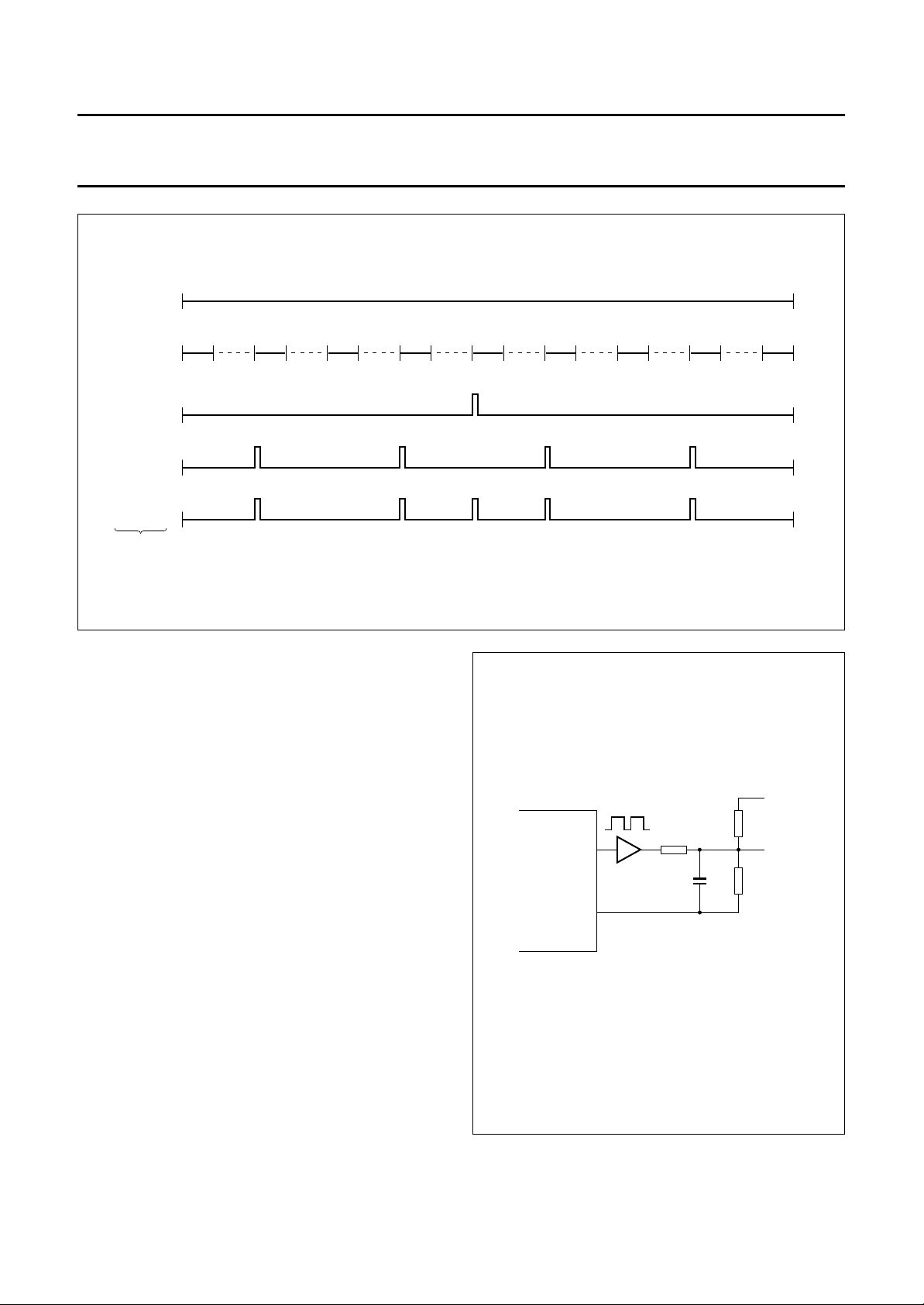
Figures 23 to 26 show the display of Space and Carriage
Return Characters in the 4 display modes, with the
Blinking function ON and OFF.
• Mode 0: No background mode. Both the Space Code
and the Carriage Return Code are displayed as
transparent (no bit) patterns, with the video signal as the
background. This is shown in Fig.23.
• Mode 1: North shadowing mode. Both codes are
displayed in the same manner as for Mode 0. This is
shown in Fig.24.
PCE84C882
• In Mode 2: Box shadowing mode. The Space Code is
displayed as a transparent pattern with selected
background colour. This will also be the background
colour of the character following the Space Code.
However, when the Space Code is used as an end bit, it
will be displayed as a transparent pattern superimposed
on the video (see Fig.30). The Carriage Return Code in
Mode 2 is also displayed as a transparent pattern
superimposed on the video signal.
• Mode 3: Frame shadowing mode. The Space Code and
the Carriage Return Code are both displayed as
transparent patterns with background colour (see
Fig.26).
CR codeSP codeCR codeSP code
Character ON
Character OFF
Fig.23 Blinking in No background (superimpose) mode.
Character ON
Character OFF
Fig.24 Blinking in North shadowing mode.
MLB397
CR codeSP codeCR codeSP code
MLB398
1996 Jan 08 34
Page 35

Philips Semiconductors Preliminary specification
Microcontroller for monitor OSD
and auto-sync applications
CR code CR codeSP codeSP code
Character ON
Fig.25 Blinking in Box shadowing mode.
Character OFF
PCE84C882
MLB399
Character ON Character OFF
Fig.26 Blinking in Frame shadowing mode.
CR codeSP codeCR codeSP code
MLB401
1996 Jan 08 35
Page 36

Philips Semiconductors Preliminary specification
Microcontroller for monitor OSD
PCE84C882
and auto-sync applications
12.4 Derivative Register 34
This register selects the 4 display modes; the active state of signal at the HSYNCN and VSYNCN inputs and the output
polarity of the FB and VOW0 to VOW2 outputs. It also enables/disables the OSD clock.
Table 25 Derivative Register 34
76543210
−−S1 S0 Hp Vp Bp EN
Table 26 Description of Derivative Register 34 bits
BIT SYMBOL DESCRIPTION
7 − These two bits are reserved.
6 −
5 S1 Display mode select bits; see Table 27.
4S0
3 Hp HSYNCN signal polarity control bit. When Hp = 0, the active level of the signal at the
HSYNCN input is LOW; this is also the default state. When Hp = 1, the active level of
the signal at the HSYNCN input is HIGH. See Fig.16.
2 Vp VSYNCN signal polarity control bit. When Vp = 0, the active level of the signal at the
VSYNCN input is LOW; this is also the default state. When Vp = 1, the active level of
the signal at the VSYNCN input is HIGH. See Fig.16.
1 Bp Output polarity control bit for FB, VOW0, VOW1 and VOW2. When Bp = 1; these
outputs are active HIGH; this is also the default state. When Bp = 0; these outputs are
active LOW.
0 EN OSD clock enable/disable bit. When EN = 1; the OSD clock is enabled. When EN = 0;
the OSD clock is disabled.
Table 27 Selection of Display Modes
S1 S0 DISPLAY MODE
0 0 Mode 0: No background (superimpose) mode. The OSD characters are superimposed
on the monitor video signals. See Fig.27.
0 1 Mode 1: North shadowing mode. The characters’ shadows are generated as if a light
source was placed North of the character (see Fig.28). Character shadowing only
appears within the cell boundary. Consequently, if Row 18 contains a bit pattern then
North shadowing will not be shown on the screen (see Fig.20). The depth of shadow
displayed is dependent upon the character size; characters with sizes of 1H/1V; 1H/2V
and 1H/3V have a depth of shadow equivalent to 1 scan line whereas a character of
size 1H/4V has a depth of shadow equivalent to 2 scan lines. Examples of characters
with North shadowing, for the 4 character sizes, are shown in Fig.29.
1 0 Mode 2: Box shadowing mode. A background dot matrix of 12 × 18 bits surrounds the
character font; where there is no foreground dot a background dot is displayed (see
Fig.30).
1 1 Mode 3: Frame shadowing mode. A background colour fills the whole screen when no
bit patterns are being displayed (see Fig.31). 1 of 8 background colours can be selected
using Derivative Register 37; the default background colour is blue.
1996 Jan 08 36
Page 37

Philips Semiconductors Preliminary specification
Microcontroller for monitor OSD
and auto-sync applications
handbook, full pagewidth
PCE84C882
MOS
FB
R
G
B
"M" : Red + Blue
"O" : Blue
"S" : Red + Green
Fig.27 Mode 0: No background (superimpose) mode.
1996 Jan 08 37
SP code
SP codeSP code
MLC077
scan
line
Page 38

Philips Semiconductors Preliminary specification
Microcontroller for monitor OSD
and auto-sync applications
handbook, full pagewidth
PCE84C882
scan
line
FB
R
G
B
1st character : Green
2nd character : Blue
Character background shadowing : Red
MLC078
Fig.28 Mode 1: North shadowing background mode.
1996 Jan 08 38
Page 39

Philips Semiconductors Preliminary specification
Microcontroller for monitor OSD
and auto-sync applications
0
1
2
3
4
5
6
7
8
9
10
11
12
13
14
15
16
17
18
(a) Character designed in character ROM
PCE84C882
MLB396
0
1
2
3
4
5
6
7
8
9
10
11
12
13
14
15
16
17
(b) 1H/2V or 1H/4V character displayed on the screen
0
1
2
3
4
5
6
7
8
9
10
11
12
13
14
15
16
17
(c) 1H/1V character displayed on the screen
0
1
2
3
4
5
6
7
8
9
10
11
12
13
14
15
16
17
(d) 1H/3V character displayed on the screen
Fig.29 Example of North shadowing mode.
1996 Jan 08 39
Page 40

Philips Semiconductors Preliminary specification
Microcontroller for monitor OSD
and auto-sync applications
handbook, full pagewidth
PCE84C882
M
FB
R
G
B
"M" : Foreground - Red + Blue
Background - Green
"O" : Foreground - Blue
Background - Red
"S" : Foreground - Red + Green
Background - Blue
Fig.30 Mode 2: Box shadowing (background) mode.
1996 Jan 08 40
SP code SP code
OS
SP code
(End)
MLC079
scan
line
Page 41

Philips Semiconductors Preliminary specification
Microcontroller for monitor OSD
and auto-sync applications
handbook, full pagewidth
PCE84C882
MOS
FB
R
G
B
"M" : Red + Blue
"O" : Blue
"S" : Red + Green
Frame background : Green
Fig.31 Mode 3: Frame shadowing mode.
1996 Jan 08 41
SP code SP code
SP code
MLC080
scan
line
Page 42

Philips Semiconductors Preliminary specification
Microcontroller for monitor OSD
PCE84C882
and auto-sync applications
12.5 Derivative Register 35
Derivative Register 35 selects the vertical starting position of the display row.
Table 28 Derivative Register 35
76543210
−−V5 V4 V3 V2 V1 V0
Table 29 Description of Derivative Register 35 bits.
BIT SYMBOL DESCRIPTION
7 − These 2 bits are reserved.
6 −
5 V5 These 6 bits enable 1 of 64 vertical start positions to be selected for the display row.
4V4
3V3
2V2
1V1
0V0
The vertical starting position is calculated as follows:
VP 4 V5 V0→()×[]horizontal scan lines×=
Where (V5 → V0) is the decimal value of the contents of Register 35; (V5 → V0) ≥ 0.
12.6 Derivative Register 36
Derivative Register 36 selects the horizontal starting position of the display row.
Table 30 Derivative Register 36
76543210
−−H5 H4 H3 H2 H1 H0
Table 31 Description of Derivative Register 36 bits
BIT SYMBOL DESCRIPTION
7 − These 2 bits are reserved.
6 −
5 H5 These 6 bits enable 1 of 64 horizontal start positions to be selected for the display row.
4H4
3H3
2H2
1H1
0H0
The horizontal starting position is calculated as follows:
HP 4 H5 H0→()5+×[]OSD clock×=
Where (H5 → H0) is the decimal value of the contents of Register 36; (H5 → H0) ≥ 2.
1996 Jan 08 42
Page 43

Philips Semiconductors Preliminary specification
Microcontroller for monitor OSD
PCE84C882
and auto-sync applications
12.7 Derivative Register 37
Derivative Register 37 selects the background colour when the OSD is in Frame shadowing mode.
Table 32 Derivative Register 37
76543210
−−−−−FRR FRG FRB
Table 33 Description of Derivative Register 37 bits
BIT SYMBOL DESCRIPTION
7 − These 5 bits are reserved.
6 −
5 −
4 −
3 −
2 FRR These three bits are used to select the background colour in Frame shadowing mode;
1 FRG
0 FRB
see Table 34. The default colour is blue.
Table 34 Selection of Background colour
FRR
(RED)
0 0 0 black
0 0 1 blue
0 1 0 green
0 1 1 cyan
100red
1 0 1 magenta
1 1 0 yellow
1 1 1 white
FRG
(GREEN)
FRB
(BLUE)
COLOUR
1996 Jan 08 43
Page 44

Philips Semiconductors Preliminary specification
Microcontroller for monitor OSD
and auto-sync applications
13 TO FORMAT THE OSD
13.1 Number of characters per row
The number of characters per row is a function of
character width. The width of the character displayed is
only dependent upon the value held in the 7-bit
programmable counter (PLLCN) and is not affected by a
change in horizontal resolution (any change in f
reflected by a linear change in the frequency of the OSD
clock).
The maximum number of characters per row can be
determined by calculating the number of OSD clock pulses
that occur during the Hsync active period and dividing the
result by the number of horizontal dots in the character
matrix (which is 12). If Hsync is assumed to be active for
85% of its cycle period then the maximum number of
characters per row (N) can be calculated as follows:
0.85 f
×
12 f
×
OSD
Hsync
N
=
-----------------------------
Hsync
will be
PCE84C882
13.3 Character size selection for different display
resolutions
To cater for the variable display resolutions (i.e. 640 x 400,
640 × 480, 800 × 600, 1024 × 768 and 1280 × 1024) of
auto-sync monitors, the PCE84C882 offers a choice of 4
different character sizes: 1H/1V, 1H/2V, 1H/3V and 1H/4V.
This allows the height of displayed characters to be of
similar size even when the monitors resolution is changed
(see Table 35).
Table 35 Recommended character size selection for
different display resolutions
RESOLUTION
640 × 400 1H/2V 11
640 × 480 1H/3V 13
800 × 600 1H/3V 11
1024 × 768 1H/4V 10
1280 × 1024 1H/4V 14
CHARACTER
SIZE
ROWS/FRAME
13.2 Number of rows per frame
The number of rows per frame is a function of character
height and the spacing between the rows of characters.
The height of a character displayed on the screen is
determined by the number of visible scan lines per frame
and the character size. The number of scan lines is
dependent upon the resolution of the monitor; character
size is selected by the user (see Section 10.1.2). The
PCE84C882 also provides a choice of four inter-line
spaces: 0H, 4H, 8H and 12H (see Section 10.1.2).
If the inter-line spacing is assumed to be zero then the
number of rows per frame (R) can be calculated by dividing
the number of visible scan lines (SL) by the character size
(CS) and dividing the result by the number of vertical dots
in the character matrix (which is 18). This can be
expressed mathematically as follows:
=
-------------------- 18 CS×
SL
R
Table 35 shows the number of rows per frame for different
horizontal resolutions.
2
C-BUS INTERFACE
14 I
The PCE84C882 has an on-chip I2C-bus interface that can
be used in master or slave mode. Full details of the I2C-bus
are given in the document
This document may be ordered using the code
9398 393 40011.
The I2C-bus interface lines SDA and SCL share the same
pins as Derivative Port lines DP20 and DP21 respectively.
Selection of the pin function as either an I2C-bus line or a
Derivative Port line is achieved using the SDAE and SCLE
bits in Derivative Register 22 (see Section 12.1). Only port
Option 2 is available for both of these pins.
“The I2C-bus and how to use it”
.
1996 Jan 08 44
Page 45

Philips Semiconductors Preliminary specification
Microcontroller for monitor OSD
and auto-sync applications
15 8-BIT COUNTER (T3)
One application for this counter is in the frequency
measurement of the Hsync signal.
The block diagram of the 8-bit counter is shown in Fig.33.
A Schmitt trigger is used at the input for noise rejection and
also to shape the input signal into a square wave. The T3
input is sampled at a frequency of1⁄3× f
clock which synchronizes the internal T3 clock and the
read operation of Derivative Register 24. The rising edge
of the input increments the ripple counter by 1.
The contents of T3 may be read using the instruction
MOV A, D24 (where D24 is Derivative Register 24). As
soon as the data is read, the counter is reset to zero. A
counter overflow or Power-on-reset also resets the
counter contents to zero.
If the rising and falling edges of the input pulse are less
than 30 ns then the minimum pulse width that the T3 input
will recognise is 3/f
+ 100 ns. If the system clock is
osc
10 MHz then the minimum pulse width is 400 ns. In some
display modes, the active pulse width of the Hsync signal
can be less than 400 ns. In this situation, extra hardware
circuitry may be necessary.
by the sample
osc
handbook, halfpage
PCE84C882
t
0.9 V
DD
0.1 V
DD
t
t
0.9 V
DD
0.1 V
DD
Fig.32 T3 input waveform.
H
r
f
t
f
t
r
t
L
MGC719
handbook, full pagewidth
T3
Power-on-reset
READ D24H
EMU
SYNCHRONISATION
CIRCUIT
sample clock
T3 COUNTER
CONTROL CIRCUIT
CK
8-BIT COUNTER
RESET
Fig.33 Block diagram of the 8-bit counter (T3).
Q0 to Q7
Data bus
MGC717
1996 Jan 08 45
Page 46

Philips Semiconductors Preliminary specification
Microcontroller for monitor OSD
and auto-sync applications
16 OUTPUT PORTS
Each I/O port line may be individually configured using one
of three mask options. The three I/O mask options are
specified below:
Option 1 Standard input/output with switched pull-up
current source; this is shown in Fig.34.
Option 2 Input/output with Open drain output; this is
shown in Fig.35.
Option 3 Push-pull output; this is shown in Fig.36.
The state of each output port after a Power-on-reset can
also be selected using the mask options. All port mask
options are given in Section 16.1.
handbook, full pagewidth
WRITE PULSE
OUTL/ORL/ANL/MOV
DATA BUS
D
MQ
MASTER
D
SLAVE
SQ
SQ
TR2
TR1
TR3
PCE84C882
V
constant
current
source
100 µA typ.
DD
I/O PORT
LINE
V
SS
ORL/ANL/MOV
IN/MOV
Fig.34 Standard I/O with pull-up transistor source (Option 1).
MLA696
1996 Jan 08 46
Page 47

Philips Semiconductors Preliminary specification
Microcontroller for monitor OSD
and auto-sync applications
WRITE PULSE
handbook, full pagewidth
OUTL/ORL/ANL
DATA BUS
D
MQ
MASTER
ORL/ANL
D
SLAVE
SQ
SQ
PCE84C882
V
DD
I/O PORT
TR1
V
SS
MLA697
IN
LINE
handbook, full pagewidth
WRITE PULSE
OUTL / ORL / ANL
DATA BUS
Fig.35 Open-drain I/O without pull-up transistor (Option 2).
TR2
D
SLAVE
SQ
SQ
TR1
V
SS
IN
D
MQ
MASTER
ORL / ANL
MLB998
constant
current
source
100 µA typ.
OUTPUT
LINE
V
DD
Fig.36 Push-pull output with pull-up transistor (Option 3).
1996 Jan 08 47
Page 48

Philips Semiconductors Preliminary specification
Microcontroller for monitor OSD
PCE84C882
and auto-sync applications
16.1 Mask options
Table 36 lists the port mask options for the PCE84C882. Table 37 is intended for customer use when ordering the device.
Table 36 Port options
OPTION
PORT PIN
CONFIGURATION RESET STATE
P00 13 1, 2 or 3 HIGH or LOW
P01 14 1, 2 or 3 HIGH or LOW
P02 15 1, 2 or 3 HIGH or LOW
P03 16 1, 2 or 3 HIGH or LOW
P04 17 1, 2 or 3 HIGH or LOW
P05 18 1, 2 or 3 HIGH or LOW
P06 19 1, 2 or 3 HIGH or LOW
P07 20 1, 2 or 3 HIGH or LOW
P10 7 1, 2 or 3 HIGH or LOW
P11 8 1, 2 or 3 HIGH or LOW
P12 10 1, 2 or 3 HIGH or LOW
P14 12 1, 2 or 3 HIGH or LOW
DP00 29 1, 2 or 3 HIGH or LOW
DP01 28 1, 2 or 3 HIGH or LOW
DP02 27 1, 2 or 3 HIGH or LOW
DP03 26 1, 2 or 3 HIGH or LOW
DP04 25 1, 2 or 3 HIGH or LOW
DP05 24 1, 2 or 3 HIGH or LOW
DP06 38 1, 2 or 3 HIGH or LOW
DP07 37 1, 2 or 3 HIGH or LOW
DP12 36 1, 2 or 3 HIGH or LOW
DP13 9 1, 2 or 3 HIGH or LOW
DP20 40 2 HIGH
DP21 39 2 HIGH
DP22 3 1, 2 or 3 HIGH or LOW
DP23 4 1, 2 or 3 HIGH or LOW
FB 1 2 or 3 HIGH or LOW
VOW2 2 2 or 3 HIGH or LOW
Table 37 Customer selected mask options
OPTION
PORT PIN
CONFIGURATION RESET STATE
P00 13
P01 14
P02 15
P03 16
P04 17
P05 18
P06 19
P07 20
P10 7
P11 8
P12 10
P14 12
DP00 29
DP01 28
DP02 27
DP03 26
DP04 25
DP05 24
DP06 38
DP07 37
DP12 36
DP13 9
DP20 40 2 S
DP21 39 2 S
DP22 3
DP23 4
FB 1
VOW2 2
1996 Jan 08 48
Page 49

Philips Semiconductors Preliminary specification
Microcontroller for monitor OSD
PCE84C882
and auto-sync applications
17 DERIVATIVE REGISTERS
The PCE84C882 has 29 Derivative Registers. The Derivative Port I/O registers are located at addresses 00 to 05H.
When DP0TR, DP1TR and DP2TR are read the data is read directly from the pin. However, when DP0R, DP1R and
DP2R are read the data is read from the port latch (see Figs 34 to 36 for the port configuration).
As the PCE84C882 has no PWM5 output the corresponding enable bit (PWM5E) in the PWME Register (address 21H)
must be set to a logic 0.
As the PCE84C882 has only one ADC channel the channel select bits (ADCS1 and ADCS0) in the ADCCN Register
(address 20H) and the pin function enable bits (ADCE1 and ADCE0) in the CON1 Register (address 22H) must be set
to the values specified in Chapter 8.
Table 38 Register map (see note 1)
ADDR
(HEX)
00 DP0TR DP07
01 DP1TR −
02 DP2TR −
03 DP0R DP07
04 DP1R −
05 DP2R −
10 PWM0 −
11 PWM1 −
12 PWM2 −
13 PWM3 −
14 PWM4 −
16 PWM6 −
17 PWM7 −
18 PWM8L −
19 PWM8H −
20 ADCCN −
REG 7 6 5 4 3 2 1 0 R/W
(X)
(X)
(X)
(1)
(X)
(X)
(X)
(X)
(X)
(X)
(X)
(X)
(X)
(X)
(X)
(X)
DP06
(X)
−
(X)
−
(X)
DP06
(1)
−
(X)
−
(X)
PWM06
(0)
PWM16
(0)
PWM26
(0)
PWM36
(0)
−
(X)
−
(X)
−
(X)
PWM86L
(0)
PWM86H
(0)
ADCS1
(0)
DP05
(X)
−
(X)
−
(X)
DP05
(1)
−
(X)
−
(X)
PWM05
(0)
PWM15
(0)
PWM25
(0)
PWM35
(0)
PWM45
(0)
PWM65
(0)
PWM75
(0)
PWM85L
(0)
PWM85H
(0)
ADCS0
(0)
DP04
(X)
−
(X)
−
(X)
DP04
(1)
−
(X)
−
(X)
PWM04
(0)
PWM14
(0)
PWM24
(0)
PWM34
(0)
PWM44
(0)
PWM64
(0)
PWM74
(0)
PWM84L
(0)
PWM84H
(0)
DAC3
(0)
DP03
(X)
DP13
(X)
DP23
(X)
DP03
(1)
DP13
(1)
DP23
(1)
PWM03
(0)
PWM13
(0)
PWM23
(0)
PWM33
(0)
PWM43
(0)
PWM63
(0)
PWM73
(0)
PWM83L
(0)
PWM83H
(0)
DAC2
(0)
DP02
(X)
DP12
(X)
DP22
(X)
DP02
(1)
DP12
(1)
DP22
(1)
PWM02
(0)
PWM12
(0)
PWM22
(0)
PWM32
(0)
PWM42
(0)
PWM62
(0)
PWM72
(0)
PWM82L
(0)
PWM82H
(0)
DAC1
(0)
DP01
(X)
−−R
DP21
(X)
DP01
(1)
DP11
(1)
DP21
(1)
PWM01
(0)
PWM11
(0)
PWM21
(0)
PWM31
(0)
PWM41
(0)
PWM61
(0)
PWM71
(0)
PWM81L
(0)
PWM81H
(0)
DAC0
(0)
DP00
(X)
DP20
(X)
DP00
(1)
DP10
(1)
DP20
(1)
PWM00
(0)
PWM10
(0)
PWM20
(0)
PWM30
(0)
PWM40
(0)
PWM60
(0)
PWM70
(0)
PWM80L
(0)
PWM80H
(0)
(2)
COMP
(0)
R
R
RW
RW
RW
RW
RW
RW
RW
RW
RW
RW
RW
RW
RW
1996 Jan 08 49
Page 50

Philips Semiconductors Preliminary specification
Microcontroller for monitor OSD
and auto-sync applications
ADDR
(HEX)
21 PWME PWM7E
22 CON1 PWM8E
23 CON2 VINT
24 T3CON T3B7
25 PLLCN −
30 DCRAR −
31 DCRTR −
32 DCRCR −
33 CON3 −
34 CON4 −
35 VPOS −
36 HPOS −
37 FRC −
REG 7 6 5 4 3 2 1 0 R/W
(0)
(0)
(0)
(0)
(X)
(X)
(X)
(X)
(X)
(X)
(X)
(X)
(X)
PWM6E
(0)
SCLE
(0)
VIEN
(0)
T3B6
(0)
PLL6
(0)
−
(X)
−
(X)
−
(X)
−
(X)
−
(X)
−
(X)
−
(X)
−
(X)
PWM5E
(0)
SDAE
(0)
−
(X)
T3B5
(0)
PLL5
(0)
DCRA5
(0)
−
(X)
DCRC5
(1)
−
(X)
S1
(0)
V5
(1)
H5
(0)
−
(X)
PWM4E
(0)
ADCE2
(0)
−
(X)
T3B4
(0)
PLL4
(0)
DCRA4
(0)
−
(X)
DCRC4
(1)
−
(X)
S0
(0)
V4
(1)
H4
(0)
−
(X)
PWM3E
(0)
ADCE1
(0)
−
(X)
T3B3
(0)
PLL3
(0)
DCRA3
(0)
DCRT3
(1)
DCRC3
(1)
BR1
(0)
Hp
(0)
V3
(1)
H3
(0)
−
(X)
PWM2E
(0)
ADCE0
(0)
P8LVL
(0)
T3B2
(0)
PLL2
(0)
DCRA2
(0)
DCRT2
(1)
DCRC2
(1)
BR0
(0)
Vp
(0)
V2
(1)
H2
(0)
FRR
(0)
PWM1E
(0)
VOW1E
(0)
P7LVL
(0)
T3B1
(0)
PLL1
(0)
DCRA1
(0)
DCRT1
(1)
DCRC1
(1)
BF1
(1)
Bp
(1)
V1
(1)
H1
(0)
FRG
(0)
PCE84C882
PWM0E
(0)
VOW0E
(0)
P6LVL
(0)
T3B0
(0)
PLL0
(0)
DCRA0
(0)
DCRT0
(1)
DCRC0
(1)
BF0
(1)
EN
(0)
V0
(1)
H0
(0)
FRB
(1)
RW
RW
RW
R
RW
RW
W
W
RW
RW
W
W
W
Notes
1. Values within parethesis show the bit state after a reset operation. ‘X’ denotes an undefined state.
2. This bit is Read only.
18 LIMITING VALUES
In accordance with the Absolute Maximum Rating System (IEC 34)
SYMBOL PARAMETER MIN. MAX. UNIT
V
DD
V
I
I
OH
I
OL
P
tot
T
amb
T
stg
supply voltage −0.3 +8.0 V
input voltage on any pin with respect to ground (VSS) −0.3 VDD+ 0.3 V
maximum source current for all port lines −−10.0 mA
maximum sink current for all port lines − 30.0 mA
total power dissipation − 1W
operating ambient temperature −25 +85 °C
storage temperature −55 +125 °C
1996 Jan 08 50
Page 51

Philips Semiconductors Preliminary specification
Microcontroller for monitor OSD
PCE84C882
and auto-sync applications
19 DC CHARACTERISTICS
=5V±10%;VSS=0V;T
V
DD
SYMBOL PARAMETER CONDITIONS MIN. TYP. MAX. UNIT
Supply
V
I
I
V
DD
DD
LU
POR
operating supply voltage 4.5 5.0 5.5 V
operating supply current f
latch-up current for all pins 50 −− mA
Power-on-reset voltage level 0.7 1.3 1.9 V
Ports P0, P1, DP0, DP1 and DP2 inputs
V
IL
V
IH
I
LI
LOW level input voltage 0 − 0.3VDDV
HIGH level input voltage 0.7VDD− V
input leakage current VSS< VI< V
Port P0 outputs
V
I
OH1
I
OH2
OL
LOW level output voltage VDD=5V; IOL=10mA −−1.2 V
HIGH level pull-up output source current VDD=5V; VO= 0.7V
HIGH level push-pull output source current VDD=5V; VO=VDD− 0.4 V −3.0 −7.0 − mA
DP00/PWM0 to DP07/PWM7 as derivative ports
I
OL
I
OH1
I
OH2
LOW level output sink current VDD=5V; VOL= 0.4 V 5.0 12.0 − mA
HIGH level pull-up output source current VDD=5V; VO= 0.7V
HIGH level push-pull output source current VDD=5V; VO=VDD− 0.4 V −3.0 −7.0 − mA
DP00/PWM0 to DP07/PWM7 as PWM outputs
I
OL
I
OH1
I
OH2
LOW level output sink current VDD=5V; VOL= 0.4 V 0.7 1.5 − mA
HIGH level pull-up output source current VDD=5V; VO= 0.7V
HIGH level push-pull output source current VDD=5V; VO=VDD− 0.4 V −0.7 −1.5 − mA
P10 to P12 and P14 outputs
I
OL
I
OH1
I
OH2
LOW level output sink current VDD=5V; VOL= 0.4 V 5.0 12.0 − mA
HIGH level pull-up output source current VDD=5V; VO= 0.7V
HIGH level push-pull output source current VDD=5V; VO=VDD− 0.4 V −3.0 −7.0 − mA
DP20/SDA and DP21/SCL outputs
I
OL
I
OH1
I
OH2
LOW level output sink current VDD=5V; VOL= 0.4 V 3.0 −− mA
HIGH level pull-up output source current VDD=5V; VO= 0.7V
HIGH level push-pull output source current VDD=5V; VO=VDD− 0.4 V −−7.0 − mA
= −25 to +85 °C; all voltages with respect to VSS; unless otherwise specified.
amb
= f
OSD
f
OSD
f
OSD
f
OSD
V
DD
V
DD
V
DD
V
DD
V
DD
= 10 MHz − 510mA
xtal
= f
= 6 MHz − 3.5 7 mA
xtal
= Stop; f
= Stop; f
=5V; VO=V
=5V; VO=V
=5V; VO=V
=5V; VO=V
=5V; VO=V
=10MHz − 36 mA
xtal
= 6 MHz − 1.5 4 mA
xtal
DD
DD
SS
DD
SS
DD
SS
DD
SS
DD
SS
−−±10 µA
−40 −100 −µA
−−140 −400 µA
−40 −100 −µA
−−140 −400 µA
−40 −100 −µA
−−140 −400 µA
−40 −100 −µA
−−140 −400 µA
−40 −100 −µA
−−140 −400 µA
DD
V
1996 Jan 08 51
Page 52

Philips Semiconductors Preliminary specification
Microcontroller for monitor OSD
PCE84C882
and auto-sync applications
SYMBOL PARAMETER CONDITIONS MIN. TYP. MAX. UNIT
VOW1/DP22; VOW0/DP23 and DP13/PWM8 as derivative output ports
I
OL
I
OH1
I
OH2
VOW1/DP22 and VOW0/DP23 as VOW outputs
I
OL
I
OH1
I
OH2
DP13/PWM8 as PWM8 output
I
OL
I
OH1
I
OH2
Outputs FB and VOW2
I
OL
I
OH1
I
OH2
DP12/ADC2 as derivative output port
I
OL
I
OH1
I
OH2
TEST/EMU;
V
IL
V
IH
I
LI
LOW level output sink current VDD=5V; VOL= 0.4 V 5.0 12.0 − mA
HIGH level pull-up output source current VDD=5V; VO= 0.7V
=5V; VO=V
V
DD
SS
DD
−40 −100 −µA
−−140 −400 µA
HIGH level push-pull output source current VDD=5V; VO=VDD− 0.4 V −3.0 −7.0 − mA
LOW level output sink current VDD=5V; VOL= 0.4 V 1.4 3.0 − mA
HIGH level pull-up output source current VDD=5V; VO= 0.7V
=5V; VO=V
V
DD
SS
DD
−40 −100 −µA
−−140 −400 µA
HIGH level push-pull output source current VDD=5 V; VO=VDD− 0.4 V −1.4 −3.0 − mA
LOW level output sink current VDD=5V; VOL= 0.4 V 1.4 3.0 − mA
HIGH level pull-up output source current VDD=5V; VO= 0.7V
=5V; VO=V
V
DD
SS
DD
−40 −100 −µA
−−140 −400 µA
HIGH level push-pull output source current VDD=5V; VO=VDD− 0.4 V −1.4 −3.0 − mA
LOW level output sink current VDD=5V; VOL= 0.4 V 1.4 3.0 − mA
HIGH level pull-up output source current VDD=5V; VO= 0.7V
=5V; VO=V
V
DD
SS
DD
−40 −100 −µA
−−140 −400 µA
HIGH level push-pull output source current VDD=5V; VO=VDD− 0.4 V −1.4 −3.0 − mA
LOW level output sink current VDD=5V; VOL= 0.4 V 5.0 12.0 − mA
HIGH level pull-up output source current VDD=5V; VO= 0.7V
=5V; VO=V
V
DD
SS
DD
−40 −100 −µA
−−140 −400 µA
HIGH level push-pull output source current VDD=5V; VO=VDD− 0.4 V −3.0 −7.0 − mA
RESET; INTN/T0; T1; HSYNCN; VSYNCN and T3
LOW level input voltage 0 − 0.3VDDV
HIGH level input voltage 0.7VDD− V
input leakage current VSS< VI< V
DD
−1.0 − +1.0 µA
DD
V
1996 Jan 08 52
Page 53

Philips Semiconductors Preliminary specification
Microcontroller for monitor OSD
PCE84C882
and auto-sync applications
20 AC CHARACTERISTICS
SYMBOL PARAMETER CONDITIONS MIN. TYP. MAX. UNIT
f
xtal
f
PXE
f
OSD
f
Hsync
f
Vsync
C
OSD
C
xtal1
C
xtal2
t
T3
Crystal oscillator frequency VDD= 5 V; T
Option 1: g
Option 2: g
= 0.4 mS 1 − 6 MHz
m
= 1.2 mS 4 − 10 MHz
m
PXE resonator frequency
Option 2: g
= 1.2 mS 1 − 5 MHz
m
OSD clock frequency VDD= 4.75 V; T
Hsync frequency duty cycle = 10 : 90 30 − 90 kHz
Vsync frequency duty cycle = 10 : 90 50 − 120 Hz
external capacitance at pin C − 0.33 −µF
external capacitance at XTAL1 (IN)
pin (PXE resonator)
external capacitance at XTAL2 (OUT)
pin (PXE resonator)
minimum pulse width period at T3
input
rising or falling edge of T3
pulse < 30 ns
= −25 to +85 °C
amb
= +70 °C 6.0 − 20 MHz
amb
− 30 100 pF
− 30 100 pF
0.4 −− µs
Analog-to-Digital (software) Converter
V
AI
ADC2 comparator analog input
voltage
V
T
AE
AFC
conversion error range −−±
conversion time (from any change in
ADC input i.e. voltage level or
enable/disable)
V
SS
− V
DD
1
⁄
2
V
LSB
−−7 µs
1996 Jan 08 53
Page 54

Philips Semiconductors Preliminary specification
Microcontroller for monitor OSD
PCE84C882
and auto-sync applications
21 DEVELOPMENT SUPPORT
Table 39 details the hardware items available for development support and Table 40 lists the development support
documentation.
Table 39 Hardware
ITEM TYPE ORDER NUMBER
LCDS Development System
Mother board - LCDS84 OM1025 9339 931 50112
Daughter board - LCD84C882 OM4835 9350 861 10112
Piggy-back version
PCA84C882B − 9350 872 50112
Table 40 Documentation
DOCUMENT NAME REPORT NUMBER
OM4873 Demo-Board Using PCE84C882 OSD microcontroller in Auto-Sync
Monitor Application
AN94049
1996 Jan 08 54
Page 55

Philips Semiconductors Preliminary specification
Microcontroller for monitor OSD
and auto-sync applications
22 PACKAGE OUTLINE
SDIP42: plastic shrink dual in-line package; 42 leads (600 mil)
D
seating plane
L
Z
e
PCE84C882
SOT270-1
M
E
A
2
A
A
1
w M
b
1
c
(e )
M
1
H
42
pin 1 index
1
DIMENSIONS (mm are the original dimensions)
A
A
A
UNIT b
mm
max.
5.08 0.51 4.0
12
min.
max.
b
1.3
0.8
0.53
0.40
b
22
E
21
0 5 10 mm
scale
cEe M
1
0.32
0.23
(1) (1)
D
38.9
38.4
14.0
13.7
1
L
M
E
3.2
15.80
2.9
15.24
17.15
15.90
e
w
H
0.181.778 15.24
Z
max.
1.73
(1)
Note
1. Plastic or metal protrusions of 0.25 mm maximum per side are not included.
OUTLINE
VERSION
SOT270-1
IEC JEDEC EIAJ
REFERENCES
1996 Jan 08 55
EUROPEAN
PROJECTION
ISSUE DATE
90-02-13
95-02-04
Page 56

Philips Semiconductors Preliminary specification
Microcontroller for monitor OSD
and auto-sync applications
23 SOLDERING
23.1 Introduction
There is no soldering method that is ideal for all IC
packages. Wave soldering is often preferred when
through-hole and surface mounted components are mixed
on one printed-circuit board. However, wave soldering is
not always suitable for surface mounted ICs, or for
printed-circuits with high population densities. In these
situations reflow soldering is often used.
This text gives a very brief insight to a complex technology.
A more in-depth account of soldering ICs can be found in
“IC Package Databook”
our
23.2 Soldering by dipping or by wave
The maximum permissible temperature of the solder is
260 °C; solder at this temperature must not be in contact
with the joint for more than 5 seconds. The total contact
time of successive solder waves must not exceed
5 seconds.
(order code 9398 652 90011).
PCE84C882
The device may be mounted up to the seating plane, but
the temperature of the plastic body must not exceed the
specified maximum storage temperature (T
printed-circuit board has been pre-heated, forced cooling
may be necessary immediately after soldering to keep the
temperature within the permissible limit.
23.3 Repairing soldered joints
Apply a low voltage soldering iron (less than 24 V) to the
lead(s) of the package, below the seating plane or not
more than 2 mm above it. If the temperature of the
soldering iron bit is less than 300 °C it may remain in
contact for up to 10 seconds. If the bit temperature is
between 300 and 400 °C, contact may be up to 5 seconds.
stg max
). If the
1996 Jan 08 56
Page 57

Philips Semiconductors Preliminary specification
Microcontroller for monitor OSD
PCE84C882
and auto-sync applications
24 DEFINITIONS
Data sheet status
Objective specification This data sheet contains target or goal specifications for product development.
Preliminary specification This data sheet contains preliminary data; supplementary data may be published later.
Product specification This data sheet contains final product specifications.
Limiting values
Limiting values given are in accordance with the Absolute Maximum Rating System (IEC 134). Stress above one or
more of the limiting values may cause permanent damage to the device. These are stress ratings only and operation
of the device at these or at any other conditions above those given in the Characteristics sections of the specification
is not implied. Exposure to limiting values for extended periods may affect device reliability.
Application information
Where application information is given, it is advisory and does not form part of the specification.
25 LIFE SUPPORT APPLICATIONS
These products are not designed for use in life support appliances, devices, or systems where malfunction of these
products can reasonably be expected to result in personal injury. Philips customers using or selling these products for
use in such applications do so at their own risk and agree to fully indemnify Philips for any damages resulting from such
improper use or sale.
26 PURCHASE OF PHILIPS I
Purchase of Philips I
components in the I2C system provided the system conforms to the I2C specification defined by
Philips. This specification can be ordered using the code 9398 393 40011.
2
C COMPONENTS
2
C components conveys a license under the Philips’ I2C patent to use the
1996 Jan 08 57
Page 58

Philips Semiconductors Preliminary specification
Microcontroller for monitor OSD
and auto-sync applications
PCE84C882
NOTES
1996 Jan 08 58
Page 59

Philips Semiconductors Preliminary specification
Microcontroller for monitor OSD
and auto-sync applications
PCE84C882
NOTES
1996 Jan 08 59
Page 60

Philips Semiconductors – a worldwide company
Argentina: IEROD, Av. Juramento 1992 - 14.b, (1428)
BUENOS AIRES, Tel. (541)786 7633, Fax. (541)786 9367
Australia: 34 Waterloo Road, NORTH RYDE, NSW 2113,
Tel. (02)805 4455, Fax. (02)805 4466
Austria: Triester Str. 64, A-1101 WIEN, P.O. Box 213,
Tel. (01)60 101-1236, Fax. (01)60 101-1211
Belgium: Postbus 90050, 5600 PB EINDHOVEN, The Netherlands,
Tel. (31)40-2783749, Fax. (31)40-2788399
Brazil: Rua do Rocio 220 - 5
CEP: 04552-903-SÃO PAULO-SP, Brazil,
P.O. Box 7383 (01064-970),
Tel. (011)821-2333, Fax. (011)829-1849
Canada: PHILIPS SEMICONDUCTORS/COMPONENTS:
Tel. (800) 234-7381, Fax. (708) 296-8556
Chile: Av. Santa Maria 0760, SANTIAGO,
Tel. (02)773 816, Fax. (02)777 6730
China/Hong Kong: 501 Hong Kong Industrial Technology Centre,
72 Tat Chee Avenue, Kowloon Tong, HONG KONG,
Tel. (852)2319 7888, Fax. (852)2319 7700
Colombia: IPRELENSO LTDA, Carrera 21 No. 56-17,
77621 BOGOTA, Tel. (571)249 7624/(571)217 4609,
Fax. (571)217 4549
Denmark: Prags Boulevard 80, PB 1919, DK-2300
COPENHAGEN S, Tel. (45)32 88 26 36, Fax. (45)31 57 19 49
Finland: Sinikalliontie 3, FIN-02630 ESPOO,
Tel. (358)0-615 800, Fax. (358)0-61580 920
France: 4 Rue du Port-aux-Vins, BP317,
92156 SURESNES Cedex,
Tel. (01)4099 6161, Fax. (01)4099 6427
Germany: P.O. Box 10 51 40, 20035 HAMBURG,
Tel. (040)23 53 60, Fax. (040)23 53 63 00
Greece: No. 15, 25th March Street, GR 17778 TAVROS,
Tel. (01)4894 339/4894 911, Fax. (01)4814 240
India: Philips INDIA Ltd, Shivsagar Estate, A Block,
Dr. Annie Besant Rd. Worli, Bombay 400 018
Tel. (022)4938 541, Fax. (022)4938 722
Indonesia: Philips House, Jalan H.R. Rasuna Said Kav. 3-4,
P.O. Box 4252, JAKARTA 12950,
Tel. (021)5201 122, Fax. (021)5205 189
Ireland: Newstead, Clonskeagh, DUBLIN 14,
Tel. (01)7640 000, Fax. (01)7640 200
Italy: PHILIPS SEMICONDUCTORS S.r.l.,
Piazza IV Novembre 3, 20124 MILANO,
Tel. (0039)2 6752 2531, Fax. (0039)2 6752 2557
Japan: Philips Bldg 13-37, Kohnan 2-chome, Minato-ku, TOKYO 108,
Tel. (03)3740 5130, Fax. (03)3740 5077
Korea: Philips House, 260-199 Itaewon-dong,
Yongsan-ku, SEOUL, Tel. (02)709-1412, Fax. (02)709-1415
Malaysia: No. 76 Jalan Universiti, 46200 PETALING JAYA,
SELANGOR, Tel. (03)750 5214, Fax. (03)757 4880
Mexico: 5900 Gateway East, Suite 200, EL PASO, TX 79905,
Tel. 9-5(800)234-7381, Fax. (708)296-8556
th
floor, Suite 51,
Netherlands: Postbus 90050, 5600 PB EINDHOVEN, Bldg. VB,
Tel. (040)2783749, Fax. (040)2788399
New Zealand: 2 Wagener Place, C.P.O. Box 1041, AUCKLAND,
Tel. (09)849-4160, Fax. (09)849-7811
Norway: Box 1, Manglerud 0612, OSLO,
Tel. (022)74 8000, Fax. (022)74 8341
Pakistan: Philips Electrical Industries of Pakistan Ltd.,
Exchange Bldg. ST-2/A, Block 9, KDA Scheme 5, Clifton,
KARACHI 75600, Tel. (021)587 4641-49,
Fax. (021)577035/5874546
Philippines: PHILIPS SEMICONDUCTORS PHILIPPINES Inc.,
106 Valero St. Salcedo Village, P.O. Box 2108 MCC, MAKATI,
Metro MANILA, Tel. (63) 2 816 6380, Fax. (63) 2 817 3474
Portugal: PHILIPS PORTUGUESA, S.A.,
Rua dr. António Loureiro Borges 5, Arquiparque - Miraflores,
Apartado 300, 2795 LINDA-A-VELHA,
Tel. (01)4163160/4163333, Fax. (01)4163174/4163366
Singapore: Lorong 1, Toa Payoh, SINGAPORE 1231,
Tel. (65)350 2000, Fax. (65)251 6500
South Africa: S.A. PHILIPS Pty Ltd.,
195-215 Main Road Martindale, 2092 JOHANNESBURG,
P.O. Box 7430, Johannesburg 2000,
Tel. (011)470-5911, Fax. (011)470-5494
Spain: Balmes 22, 08007 BARCELONA,
Tel. (03)301 6312, Fax. (03)301 42 43
Sweden: Kottbygatan 7, Akalla. S-164 85 STOCKHOLM,
Tel. (0)8-632 2000, Fax. (0)8-632 2745
Switzerland: Allmendstrasse 140, CH-8027 ZÜRICH,
Tel. (01)488 2211, Fax. (01)481 77 30
Taiwan: PHILIPS TAIWAN Ltd., 23-30F, 66, Chung Hsiao West
Road, Sec. 1. Taipeh, Taiwan ROC, P.O. Box 22978,
TAIPEI 100, Tel. (886) 2 382 4443, Fax. (886) 2 382 4444
Thailand: PHILIPS ELECTRONICS (THAILAND) Ltd.,
209/2 Sanpavuth-Bangna Road Prakanong,
Bangkok 10260, THAILAND,
Tel. (66) 2 745-4090, Fax. (66) 2 398-0793
Turkey:Talatpasa Cad. No. 5, 80640 GÜLTEPE/ISTANBUL,
Tel. (0212)279 27 70, Fax. (0212)282 67 07
Ukraine: Philips UKRAINE, 2A Akademika Koroleva str., Office 165,
252148 KIEV, Tel.380-44-4760297, Fax. 380-44-4766991
United Kingdom: Philips Semiconductors LTD.,
276 Bath Road, Hayes, MIDDLESEX UB3 5BX,
Tel. (0181)730-5000, Fax. (0181)754-8421
United States:811 East Arques Avenue, SUNNYVALE,
CA 94088-3409, Tel. (800)234-7381, Fax. (708)296-8556
Uruguay: Coronel Mora 433, MONTEVIDEO,
Tel. (02)70-4044, Fax. (02)92 0601
Internet: http://www.semiconductors.philips.com/ps/
For all other countries apply to: Philips Semiconductors,
International Marketing and Sales, Building BE-p,
P.O. Box 218, 5600 MD EINDHOVEN, The Netherlands,
Telex 35000 phtcnl, Fax. +31-40-2724825
SCDS47 © Philips Electronics N.V. 1996
All rights are reserved. Reproduction in whole or in part is prohibited without the
prior written consent of the copyright owner.
The information presented in this document does not form part of any quotation
or contract, is believed to be accurate and reliable and may be changed without
notice. No liability will be accepted by the publisher for any consequence of its
use. Publication thereof does not convey nor imply any license under patent- or
other industrial or intellectual property rights.
Printed in The Netherlands
453061/1100/01/pp60 Date of release: 1996 Jan 08
Document order number: 9397 750 00552
 Loading...