

Page 1
INTEGRATED CIRCUITS
DATA SH EET
PCD6001
Digital telephone answering
machine chip
Product specification
Supersedes data of 2001 Feb 05
File under Integrated Circuits, IC17
2001 Apr 17
Page 2

Philips Semiconductors Product specification
Digital telephone answering machine chip PCD6001
CONTENTS
1 FEATURES
2 APPLICATION SUMMARY
2.1 Metalink emulation
3 GENERAL DESCRIPTION
4 ORDERING INFORMATION
5 BLOCK DIAGRAM
6 PINNING INFORMATION
6.1 Pinning
6.2 Pin description
6.3 Pin types
7 FUNCTIONAL DESCRIPTION
7.1 Architecture
7.2 I/O summary
7.3 Overview of functional description
8 POWER SUPPLY, RESET AND START-UP
8.1 Power supply
8.2 Reset and start-up
9 TICB - GENERATION AND SELECTION OF
SYSTEM CLOCKS
9.1 Microprocessor, DSP, CODEC and IOM clock
generation
9.2 System clocks
9.3 Real-Time Clock generation
10 THE MICROCONTROLLER
10.1 Microcontroller architecture
10.2 Memory mapping
10.3 SFR mapping
10.4 Microcontroller interrupts
10.5 Interface to DSP
10.6 Interface to Real-Time Clock (RTC)
10.7 Interface to the Memory Control Block (MCB)
10.8 The test registers CDTRx, PMTRx and TCTRL
10.9 Interface to Timing and Control Block (TICB)
10.10 Power and Interrupt Control Register (PCON)
10.11 I2C-bus
10.12 MSK modem
10.13 LE control
11 DSP I/O REGISTERS
11.1 Interface to CODEC
12 EXTERNAL MEMORY INTERFACE
12.1 Supported flash memories
12.2 DTAM external interface during target
debugging
13 THE CODECs
13.1 Definitions
13.2 CODEC architecture
14 ANALOG VOLTAGE REFERENCE (AVR)
14.1 Bandgap reference
14.2 Analog Voltage Source (AVS)
15 IOM
15.1 Features
15.2 Pin description
15.3 Functional description
15.4 IOM data buffers
15.5 IOM Control Register (IOMC)
15.6 Timing
16 EXTERNAL I/O INTERFACES
16.1 External analog interfaces
16.2 External digital Interfaces
17 ELECTRICAL CHARACTERISTICS
17.1 Limiting values
17.2 Supply characteristics
17.3 Digital I/O
17.4 Analogsuppliesandgeneral purposeADC and
DAC
17.5 CODECs
18 APPLICATION DIAGRAMS
19 PACKAGE OUTLINE
20 SOLDERING
20.1 Introduction to soldering surface mount
packages
20.2 Reflow soldering
20.3 Wave soldering
20.4 Manual soldering
20.5 Suitability of surface mount IC packages for
wave and reflow soldering methods
21 DATA SHEET STATUS
22 DEFINITIONS
23 DISCLAIMERS
24 PURCHASE OF PHILIPS I2C COMPONENTS
2001 Apr 17 2
Page 3

Philips Semiconductors Product specification
Digital telephone answering machine chip PCD6001
1 FEATURES
• Excellent speech quality at average:
2.6, 3.2 or 5.2 kbits/s compression rate
• Excellent background noise suppression for speech
quality improvement
• Speech compression rate selection: 2.6, 3.2 or
5.2 kbits/s
• Speech decompression rate selection: 2.6, 3.2 or
5.2 kbits/s
• Variable playback speed: 50%,100% and 200% of real
time
• Voice prompt playback
• Philips International Language Library (PILL) support
tools available; coding at 2.6, 3.2 or 5.2 kbits/s
• Voice operated start message recording (VOX)
• Call progress detection by busy tone detection and
programmable silence detection
• Recording time of minimum 20 minutes in 4-Mbit flash
memory (at 3.2 kbits/s)
• Excellent true full-duplex handsfree performance
provided by Philips ‘phlux’ algorithm
• On-hook caller ID detection according to Bell 202 and
V.23 standards, as well as DTMF caller ID support
• Caller Alerting Signal (CAS) - caller ID level 2
• Dual tone generation for DTMF, melody tones and
information tones
• Optional dial tone detection, and optional ringing
detection using hardware Caller Identification (CID)
interface
• DTMF detection (for remote control function) with local
echo canceller for high reliability
• Digital volume control
• Mixeddigital/analog adaptivelimitand/orlevelcontrolof
audio input signals
• Programmable analog CODEC gainfor easy interfacing
• Internal 80C51 microcontroller can operate as system
controller; with selectable operating frequencies
between 1 and 21 MHz
• Internal 80C51 microcontroller emergency operation
down to2.2 V eliminatesthe needfor externaldiallersin
telephone answering machine applications
• Standard 80C51 developmenttools allow fast design of
Man-Machine-Interface (MMI) features
• On-board Minimum Shift Keying (MSK) modem for
CT0/CT1 applications
• Two integrated differential bit stream Analog-to-Digital
Converters (ADCs) for high quality audio input
• Two integrated differential bitstream Digital-to-Analog
Converters (DACs) for high quality audio output
• Software selectable auxiliary CODEC input channel
• Up to 38 generalpurpose digital I/O lines (mostof them
bidirectional) includingI2C-bus, availablefor connection
to keyboard, display, line interface, etc.
• On-chip 2-channel time multiplexed 8-bit general
purpose ADC for e.g. parallel set detection and battery
voltage measurement
• On-chip 8-bit general purpose DAC for e.g. speaker
amplifier volume control
• Day and time stamp possibility using built-in Real-Time
Clock
• Flexible speech memory interface for connection of
several types of speech flash memory (serial, CAD or
parallel) and DRAM
• I2C master/slave bus for peripheral control or I2C-bus
speech memory access
• Extensive power management support for battery and
emergency operation, also allowing portable (voice
memo) applications
• Digital IOM A/u-law interface for Slave or Master mode
operation at various bit rates
• Emergency operation from telephone line power only;
microprocessor and DTMF generator continue to
operate in this mode
• On-chip software switchable supply voltage for electret
microphone
• Single low supply voltage (2.2 to 2.8 V)
• Built-in single low-frequency, low-power, crystal or
ceramic resonator oscillator and on-chip PLL to reduce
EMI
• Stand-alone operation with low cost PAL, NTSC and
DTMF crystals
• API providing flash memory management functions
such as speech, telephone or CID data storage
• Pin and software compatible with the PCD6002
OTP-device (see Application note for restrictions).
2001 Apr 17 3
Page 4

Philips Semiconductors Product specification
Digital telephone answering machine chip PCD6001
2 APPLICATION SUMMARY
The PCD6001 can be used in various applications, some
of which are listed below. Refer to Chapter 18 for the
corresponding outline application diagrams.
• Stand-alone digital answering machine; with handsfree
• Feature phone with integrated digital answering
machine and full-duplex handsfree
• Dual-line digital answering machines
• Analog cordless applications such as CT0/1 base
stations; with handsfree and MSK modem function for
RF digital data transmission
• Portable voice memo recorders
• Automotive applications- carstatus announcements for
example
• Low-cost desktop video conferencing
• IOM master/slave interface to connect directly to digital
systems like ISDN and DECT.
2.1 Metalink emulation
Metalink emulation is supported with the standard
package.
3 GENERAL DESCRIPTION
The PCD6001integrates all the digitaland analog speech
management and processing functions required for a
feature-phone with integrated digital answering machine,
or a stand-alone digital answering machine into a single
low-cost chip.
Key hardware features which give the chip distinct
advantages in performance and application over
competitive solutions include:
• The flexibility to change the MMI
• An easy-to-program standard 80C51 microcontroller
with 32-kbyte internal ROM memory
• High 80C51microprocessor powerfor systemcontroller
functions of CT0/CT1 system control functions
• Up to 38 generalpurpose I/O lines for peripheral control
• I2C-bus interface
• Flexible flash memory control to interface to several
types of serial and parallel flash memory
• Two integrated 16-bit bitstream audioCODECs for true
full-duplex handsfreeoperation or dual-line stand-alone
answering machine operation
• Internal Digital Speech Processor (DSP) for excellent
‘HARMONY’ sinusoidal speech compression,
decompression and variable playback speed
• Embedded DTMF detection, call progress detection,
voice operated recording (VOX)
• High quality caller ID FSK demodulation and Caller
Alerting Signal (CAS) detection for CID level 2
• Two channel telephone line input for caller ID FSK and
audio interfacing.
Philips provides a sophisticated API running on the
internal 80C51, allowing product developers to design
their MMIs quickly to suit particular applications. The API
takes care of all flash memory and DSP management
tasks and can be enhanced on request.
For the pre-recorded voice prompts, the Philips
International Language Library (PILL) tools are available
for astandard multimediaPC platform underWindows 95.
These tools provide a way to compile a range of
multi-lingual voice prompts for efficient storage in the
speech (flash) memory. The PILL tools support various
languages and their grammar adaptations.
4 ORDERING INFORMATION
TYPE
NUMBER
PCD6001H QFP80 plastic quadflat package;80 leads (leadlength 1.95 mm);
PCD6001U U/10 sawn wafer on Film Frame Carrier (delivery as Known
2001 Apr 17 4
NAME DESCRIPTION VERSION
body 14 × 20 × 2.8 mm
Good Dies)
PACKAGE
TEMPERATURE
RANGE (°C)
SOT318-2 −25 to +70
−−25 to +70
Page 5

Philips Semiconductors Product specification
Digital telephone answering machine chip PCD6001
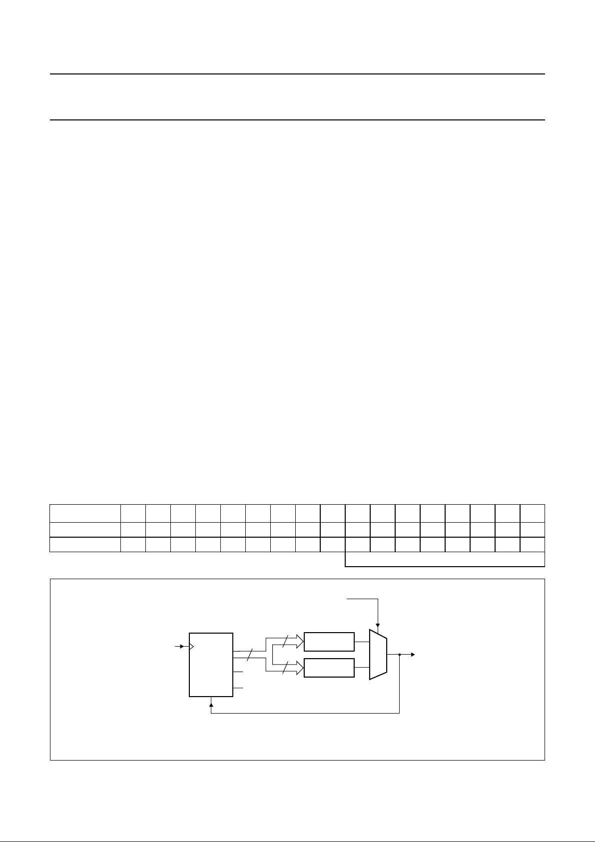
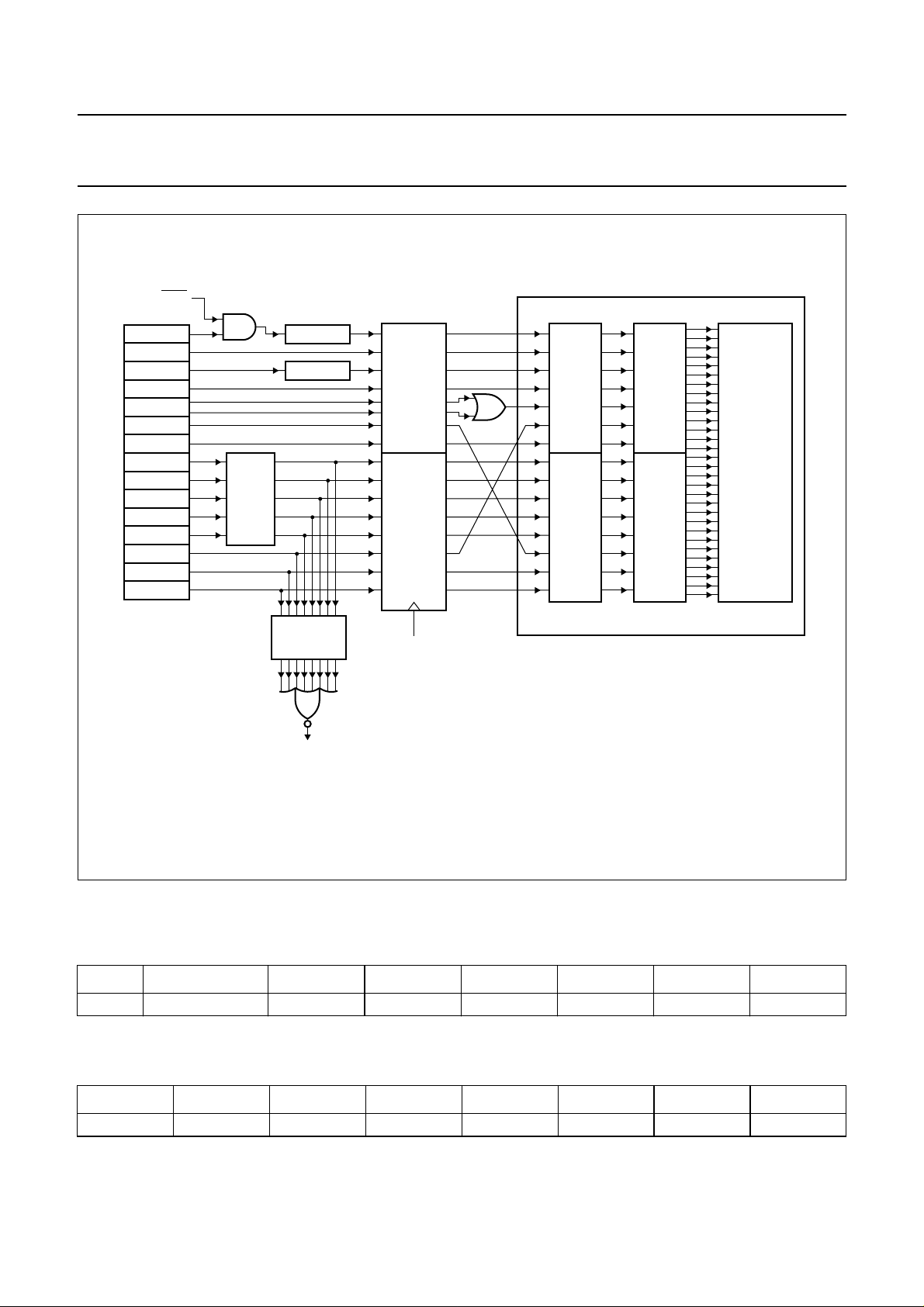
5 BLOCK DIAGRAM
handbook, full pagewidth
V
DDA
V
SSA
XTAL2
XTAL1
V
BGP
V
REF
V
MIC
AD1IN
AD0IN
DAOUT
LIFMOUT
LIFPOUT
LIFPIN
LIFMIN1
LIFMIN2
SPKRP
SPKRM
MICP
MICM
V
34
28
41
42
29
30
27
32
31
33
38
39
35
37
36
23
24
25
26
V
DDPLL
SSPLL
43 40 53 12 44
WAKE-UP
RSTANA
OSCILLATOR
and PLL
ANALOG
VOLTAGE
REFERENCE
and SUPPLY
GENERAL
PURPOSE
A/D and D/A
CODEC 1
(ANALOG)
CODEC 2
(ANALOG)
V
DD3V1
MICROCONTROLLER
events
CLK
TICB
PCD6001
CODEC 1
(DIGITAL)
CODEC 2
(DIGITAL)
V
µC_CLK
wake-up
DSPCLK
DD3V2
80C51
idle
V
DD3V3
DMI
DSP
plus
ROM,
RAM
MAIN and
AUX RAM
WATCHDOG
V
SS3V1
13 61 22
ALE, RDN, WRN
PSEN
P4.3
P0
MA
P2
main bus
MCB
I2C-
BUS
MSKIOM
V
SS3V2
32 KBYTE
ROM
AND
EXTERNAL
INTERFACE
P4
P1
V
SS3V3
11 to 4
80 to 73
72 to 65
14 to 18
54
55
3
2
62
1
64
63
56
57
58
59
60
19
20
21
TST
RSTIN
ALE
EA
MA7 to MA0
P2.7 to P2.0
P0.7 to P0.0
P4.3
PSEN
WR
RD
P4.0/LE
P4.1/FSK
P4.2/FSO
P4.4/FSI
P4.5/GPC
P1.0/EX2 to
P1.4/EX6
P1.5
P1.6/SCL
P1.7/SDA
46
45
P3.1/
MOUT1/
DCK
P3.0/
MOUT0/
DO
Fig.1 Block diagram.
2001 Apr 17 5
P3.2/
EX0N
47
P3.3/
EX1N
P3
52
51
50
49
48
MGT427
P3.5/
T1
P3.4/
T0
P3.7/
MIN/
DI
P3.6/
MOUT2/
FSC
Page 6

Philips Semiconductors Product specification
Digital telephone answering machine chip PCD6001
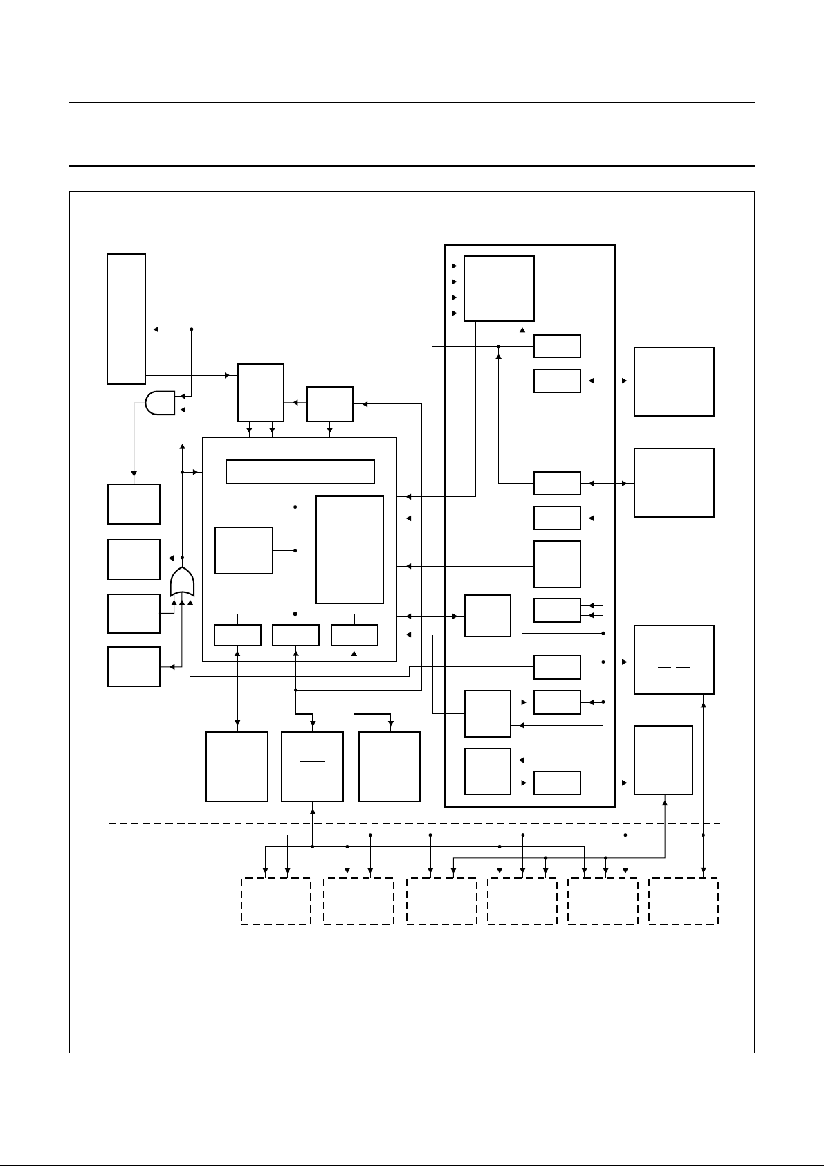
6 PINNING INFORMATION
6.1 Pinning
handbook, full pagewidth
PSEN
EA
ALE
MA0
MA1
MA2
MA3
MA4
MA5
MA6
MA7
V
DD3V2
V
SS3V1
P1.0/EX2
P1.1/EX3
P1.2/EX4
P1.3/EX5
P1.4/EX6
P1.5
P1.6/SCL
P1.7/SDA
V
SS3V3
SPKRP
SPKRM
P2.4
P2.3
P2.2
P2.1
P2.0
P0.7
P0.6
P0.5
P0.4
P0.3
P0.2
P0.1
P2.7
P2.6
P2.5
80
79
78
77
76
75
74
73
1
2
3
4
5
6
7
8
9
10
11
12
13
14
15
16
17
18
19
20
21
22
23
24
PCD6001
71
72
70
69
68
67
P0.0
66
65
WR
64
RD
63
P4.3
62
V
61
SS3V2
P4.5/GPC
60
P4.4/FSI
59
P4.2/FSO
58
P4.1/FSK
57
P4.0/LE
56
RSTIN
55
TST
54
V
53
DD3V1
P3.7/MIN/DI
52
P3.6/MOUT2/FSC
51
P3.5/T1
50
P3.4/T0
49
P3.3/EX1N
48
P3.2/EX0N
47
P3.1/MOUT1/DCK
46
P3.0/MOUT0/DO
45
V
44
DD3V3
V
43
DDPLL
XTAL1
42
XTAL2
41
25
26
27
28
29
30
31
32
MICP
MICM
MIC
V
SSA
V
BGP
V
REF
V
AD0IN
AD1IN
Fig.2 Pin configuration.
2001 Apr 17 6
33
V
DAOUT
34
DDA
35
LIFPIN
36
37
LIFMIN2
LIFMIN1
38
39
LIFPOUT
LIFMOUT
40
SSPLL
V
MGT428
Page 7

Philips Semiconductors Product specification
Digital telephone answering machine chip PCD6001
6.2 Pin description Table 1 QFP80 package
SYMBOL PIN I/O
RESET
STATE
PIN TYPE
(1)
DESCRIPTION
PSEN 1 O H ucp4mthuwh program store enable (80C51)
EA 2 I Z ucp4mthuwh external access NOT (80C51)
ALE 3 O H ucp4mthuwh address latch enable signal (80C51)
MA0 4 O L ops10c general purpose output;
MA1 5 O L ops10c general purpose output;
MA2 6 O L ops10c general purpose output;
MA3 7 O L ops10c general purpose output;
MA4 8 O L ops10c general purpose output;
MA5 9 O L ops10c general purpose output;
MA6 10 O L ops10c general purpose output;
MA7 11 O L ops10c general purpose output;
V
DD3V2
V
SS3V1
12 power supply positive supply 2 (3.0 V) for digital circuitry
13 power supply ground supply 1 for digital circuitry
EA = 1; add_low; EA = 0
EA = 1; add_low; EA = 0
EA = 1; add_low; EA = 0
EA = 1; add_low; EA = 0
EA = 1; add_low; EA = 0
EA = 1; add_low; EA = 0
EA = 1; add_low; EA = 0
EA = 1; add_low; EA = 0
P1.0/EX2 14 I/O H ucp4mthuwh 80C51 port pin/EX2 input
P1.1/EX3 15 I/O H ucp4mthuwh 80C51 port pin/EX3 input
P1.2/EX4 16 I/O H ucp4mthuwh 80C51 port pin/EX4 input
P1.3/EX5 17 I/O H ucp4mthuwh 80C51 port pin/EX5 input
P1.4/EX6 18 I/O H ucp4mthuwh 80C51 port pin/EX6 input
P1.5 19 I/O H ucp4mthuwh 80C51 port pin
P1.6/SCL 20 I/O Z I
P1.7/SDA 21 I/O Z I
V
SS3V3
22 power supply ground supply 3 for digital circuitry
2
C400k 80C51 port pin/I2C-bus clock
2
C400k 80C51 port pin/I2C-bus data
SPKRP 23 O Z ana positive output to speaker from CODEC2 (handsfree)
SPKRM 24 O Z ana negative output to speaker from CODEC2 (handsfree)
MICP 25 I 0.625 V ana positive input from microphone to CODEC2 (handsfree)
MICM 26 I 0.625 V ana negative input from microphone to CODEC2 (handsfree)
V
V
V
V
MIC
SSA
BGP
REF
27 O Z ana positive microphone supply voltage (2 V)
28 power supply ground supply voltage for analog circuits
29 O 1.25 V band gap output voltage (V
30 O 2.00 V ana reference voltage (V
REF
)
BGP
)
AD0IN 31 I − ana analog input channel 1 for general purpose ADC
AD1IN 32 I − ana analog input channel 2 for general purpose ADC
DAOUT 33 O 0.5V
V
DDA
34 power supply positive supply (2.5 V) for analog circuits
ana analog output channel for general purpose D/A converter
DDA
LIFPIN 35 I 0.625 V ana positive analog input of CODEC1 (line CODEC)
LIFMIN2 36 I 0.625 V ana negative analog input 2 of CODEC1 (line CODEC)
LIFMIN1 37 I 0.625 V ana negative analog input 1 of CODEC1 (line CODEC)
LIFMOUT 38 O Z ana negative analog output of CODEC1 (line CODEC)
2001 Apr 17 7
Page 8
Philips Semiconductors Product specification
Digital telephone answering machine chip PCD6001
SYMBOL PIN I/O
RESET
STATE
PIN TYPE
(1)
DESCRIPTION
LIFPOUT 39 O Z ana positive analog output of CODEC1 (line CODEC)
V
SSPLL
40 power supply ground supply for XTAL clock and PLL circuitry
XTAL2 41 O running ana crystal oscillator output
XTAL1 42 I − ana crystal oscillator input
V
DDPLL
V
DD3V3
43 power supply positive supply (2.5 V) for XTAL clock and PLL circuitry
44 power supply positive supply 3 (3.0 V) for digital circuitry
P3.0/MOUT0/DO 45 I/O H ucp4mthuwh 80C51 port pin/MSK output 0/IOM data output
P3.1/MOUT/DCK 46 I/O H ucp4mthuwh 80C51 port pin/MSK output 1/IOM DCK signal
P3.2/EX0N 47 I/O H ucp4mthuwh 80C51 port pin/EX0N input
P3.3/EX1N 48 I/O H ucp4mthuwh 80C51 port pin/EX1N input
P3.4/T0 49 I/O H ucp4mthuwh 80C51 port pin/Timer 0 input
P3.5/T1 50 I/O H ucp4mthuwh 80C51 port pin/Timer 1 input
P3.6/MOUT2/FSC 51 I/O H ucp4mthuwh 80C51 port pin/MSK output 2/IOM FSC signal
P3.7/MIN/DI 52 I/O H ucp4mthuwh 80C51 port pin/MSK input/IOM data input
V
DD3V1
53 power supply positive supply 1 (2.5 V) for digital circuitry
TST 54 I − iptd test input (recommended to be connected to ground)
RSTIN 55 I − ipth reset in
P4.0/LE 56 I/O L ucp4mthuwh general purpose I/O/LCD enable, configured as ODafter
reset
P4.1/FSK 57 I/O Z ucp4mthuwh general purpose I/O/Flash Serial Clock, configured
as OD after reset
P4.2/FSO 58 I/O Z ucp4mthuwh general purpose I/O/Flash Serial Out, configured as OD
after reset
P4.4/FSI 59 I/O Z ucp4mthuwh general purpose I/O/Flash Serial In, configured as OD
after reset
P4.5/GPC 60 I/O L ucp4mthuwh general purpose I/O/GP clock output (crystal clock or
microcontroller clock), configured as OD after reset
V
SS3V2
61 power supply negative supply 2 (ground) for digital circuitry
P4.3 62 I/O Z ucp4mthuwh general purpose I/O, configured as OD after reset
RD 63 O Z ucp4mthuwh 80C51 read NOT, configured as OD after reset
WR 64 O Z ucp4mthuwh 80C51 write NOT, configured as OD after reset
P0.0 65 I/O Z uceda4mtuwh 80C51 Port 0 input/output
P0.1 66 I/O Z uceda4mtuwh 80C51 Port 0 input/output
P0.2 67 I/O Z uceda4mtuwh 80C51 Port 0 input/output
P0.3 68 I/O Z uceda4mtuwh 80C51 Port 0 input/output
P0.4 69 I/O Z uceda4mtuwh 80C51 Port 0 input/output
P0.5 70 I/O Z uceda4mtuwh 80C51 Port 0 input/output
P0.6 71 I/O Z uceda4mtuwh 80C51 Port 0 input/output
P0.7 72 I/O Z uceda4mtuwh 80C51 Port 0 input/output
P2.0 73 O L ucp4mthuwh general purpose output,
P2.1 74 O L ucp4mthuwh general purpose output,
EA = 1; add_high; EA = 0
EA = 1; add_high; EA = 0
2001 Apr 17 8
Page 9
Philips Semiconductors Product specification
Digital telephone answering machine chip PCD6001
SYMBOL PIN I/O
RESET
STATE
PIN TYPE
(1)
P2.2 75 O L ucp4mthuwh general purpose output,
P2.3 76 O L ucp4mthuwh general purpose output,
P2.4 77 O L ucp4mthuwh general purpose output,
P2.5 78 O L ucp4mthuwh general purpose output,
P2.6 79 O L ucp4mthuwh general purpose output,
P2.7 80 O L ucp4mthuwh general purpose output,
Note
1. The pin type codes are explained in Section 6.3.
6.3 Pin types
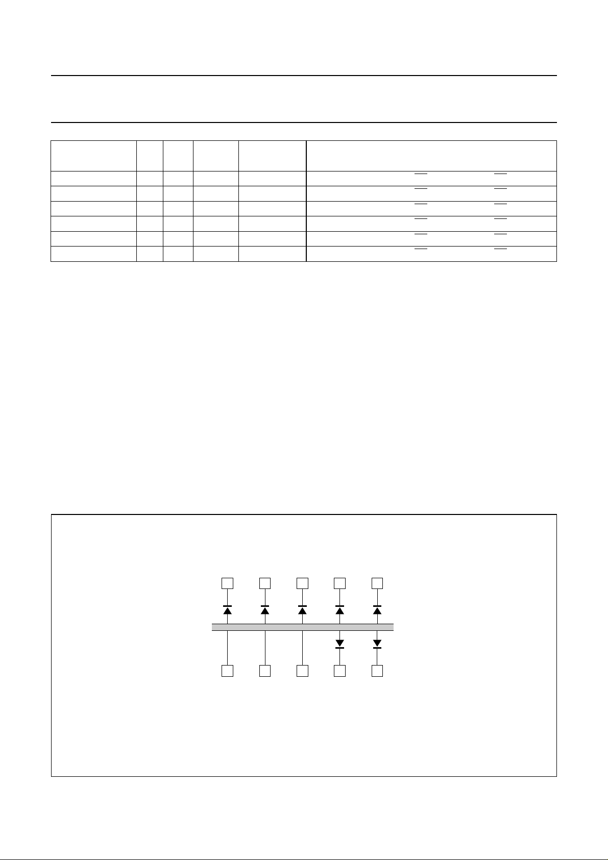
6.3.1 POWER SUPPLY PINS
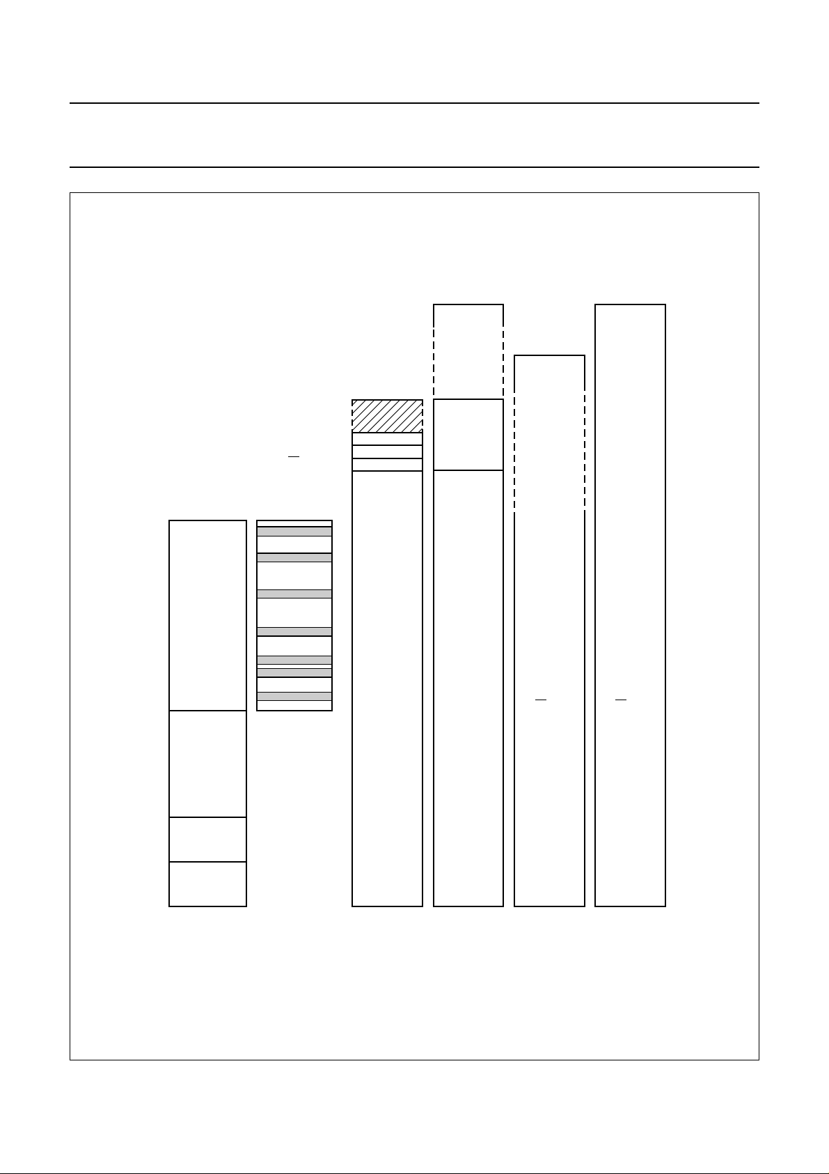
There are 6 different power supply domains (see Fig.3):
• Digital core circuit (2.5 V): V
• Digital periphery circuit (3.0 V): V
V
DD3V3/VSS3V3
• PLL circuits and crystal oscillator (2.5 V): V
V
SSPLL
• Analog circuits (2.5 V): V
DD3V1/VSS3V1
and V
DDA
DD3V2/VSS3V2
DDPLL
.
SSA
and
and
All VSSpins must beconnected to the same ground plane
on the Printed-Circuit Board (PCB). All 2.5 V VDD pins
must beconnected tothe samepower supply.All VDDpins
have tobe separatelydecoupled, accordingto Chapter 18.
6.3.2 ANALOG PINS
• ana: full ESD protected analog I/O pad (double
protection diode).
6.3.3 DIGITAL PINS
• ucp4mthuwh: 4 mA 80C51 I/O pins
• uceda4mtuwh: 4 mA 80C51 I/O pins with input enable
• iptd: input pad buffer; pull-down
• ipth: input pad buffer with Schmitt trigger
• ops10c: outputpad; push-pull; 4 mA outputdrive; 10 ns
slew control
• I2C400k: bidirectional open-drain I2C-bus compatible
pad.
DESCRIPTION
EA = 1; add_high; EA = 0
EA = 1; add_high; EA = 0
EA = 1; add_high; EA = 0
EA = 1; add_high; EA = 0
EA = 1; add_high; EA = 0
EA = 1; add_high; EA = 0
V
handbook, halfpage
DD3V1
V
SS3V1
V
DD3V2
V
SS3V2
V
DD3V3
V
SS3V3
Fig.3 PCD6001 chip supply rails with protection diodes.
2001 Apr 17 9
V
DDPLL
V
SSPLL
V
DDA
V
SSA
MGT429
Page 10

Philips Semiconductors Product specification
Digital telephone answering machine chip PCD6001
7 FUNCTIONAL DESCRIPTION
7.1 Architecture
ThePCD6001architecture isbased onan embedded8-bit
80C51 microcontroller, a Philips ‘REAL’ DSP core, two
high quality AD/DA CODECs and a 32-kbyte ROM
microcontroller memory. Refer to the block diagram in
Chapter 5.
The most important DSP peripherals are the:
• CODECs
• DSP program ROM
• DSP RAM
• IOM interface.
The most important microcontroller peripherals are the:
• Memory Control Block (MCB)
• Watchdog Timer
• General purpose ports
• I2C-bus interface
• MSK block (used for digital data transfer and analogue
cordless applications).
The MCB, through Ports P0, P2, P4 and Memory
Address (MA) can interface to various types of flash
memory including serial, parallel or multiplexed
command/address/data. Most of the peripherals are
controlled via microcontroller special function registers.
The microcontroller initializes and controls the:
• DSP via the DSP to Microcontroller Interface (DMI)
• Speech flash memory via the Memory Control
Block (MCB), and P0/P4 port pins
• Clock and power settings via the Timing and Control
Block (TICB)
• Analog sectionvia its SpecialFunction Registers (SFR).
7.2 I/O summary
All digital I/O for peripherals such as keyboard, display,
line interface and others are handled by the
microcontroller via ports P0, P1, P2, P3, P4, and MA.
Port 2 and MA provide 16 general purpose output-only
lines (not bit-addressable, push-pull, 4 mA) to drive
peripherals.These portscan beused forperipheralcontrol
if EAis logic 1. The4 mA drivinglevel should beadequate
to drive a low power LED directly if required.
In addition to these 16 output-only lines, 16 general
purpose I/O lines are provided by Ports 1 and 3. Port 1
can handle 5 external interrupts (P1.0 to P1.4) that are
also HIGH/LOWinterrupt level programmable. Port 1also
contains the I2C-bus. Port 3 can handle an additional
2 external interrupts (P3.2 and P3.3) which are active
LOW only. The Timer 0 and Timer 1 inputs are available
on Port 3 as for the standard 80C51. Ports 1 and 3 are
80C51 weak pull-up I/O lines with a 4 mA sink capability,
with the exception of the I2C-bus lines P1.6 and P1.7
which are open-drain. If the P3 alternate port function for
the MSK modem is chosen then the standard I/O is not
available on pins P3.0, P3.1, P3.6 and P3.7.
Port 4 lines are 6 more general purpose I/O. They will be
configured as open-drain after reset. These open-drains
can be connected via pull-up resistors to the telephone
system supply or to the mains AC supply. If a flash
memory with a different supply voltage (V
DD_FLASH
up
to 3.3 V) is connected, P4.3 can be pulled-up to this
voltage. This is required such that the Chip Enable
Not (CEN) input of a flash deviceis equal to V
DD_FLASH
to
reduce the standby power consumption. All other Port 4
pins should not be pulled up to a voltage higher than
V
DD_DTAM
.
In case a CAD flash is used, P4.4 and P4.5 are free
bit-addressable ports.
All P4 pins also can be configured to push-pull via the
register P4CFG. This brings the total of I/O lines to 38 (of
which 16 are output only).
In case an I2C-bus LCD driver is used, P4.0, at which
a Latch Enable (LE) function is provided for 68xxx family
microcontroller peripherals, is an additional free
bit-addressable open-drain I/O port.
The analog interfacing for the PCD6001 consists of the
analog audio I/O of the 2 CODECs and 2 additional
general purpose analog-to-digital inputs and a general
purpose digital-to-analog outputfor voltage measurement
and control respectively. Furthermore a stabilized
microphone supply output V
is provided which can be
MIC
switched on/off for power control.
One audio CODEC is dedicated for the PSTN line
communication (CODEC1). This line CODEC has a
differential low ohmic analog output which consists of
LIFPOUT and LIFMOUT. In case only one of the
differential outputs is used, LIFPOUT should be chosen,
since the Emergency modeDTMF signal is also available.
2001 Apr 17 10
Page 11

Philips Semiconductors Product specification
Digital telephone answering machine chip PCD6001
The line CODEC has 3 inputs which are configurable as
2 single-ended inputs LIFMIN1 and LIFMIN2 that can be
selected by software control, while LIFPIN is AC coupled
to ground. It is also possible to use one of the LIFMIN
inputs (leaving theother unconnected) in conjunction with
the LIFPIN input as a differential input, in case a high
CMRR is required.
The second CODEC is dedicated for a local microphone
and loudspeaker connection (CODEC2). This handsfree
CODEC has a differential low ohmic analog output which
consists of SPKRP andSPKRM.This output can be used
either differential or single ended. The speaker output
impedance and driving level is not suitable to directly
connect a speaker. The handsfree CODEC has a
differential microphone input which consists of MICP and
MICM. This differential input features a fixed 16 dB
microphone preamplifier.
Both theline and handsfreeCODEC outputshaveon-chip
filtering for outof band signals suchthat no external filters
are required.
There are 2 × 8-bit analog-to-digital inputs AD0IN and
AD1IN for voltage measurements which can be used for
parallelset detectionalgorithms orbattery control.An 8-bit
DAC output DAOUT can provide an analog peripheral
control signal.
7.3 Overview of functional description
The detailedfunctional descriptionis divided intoseparate
chapters covering the major functional blocks, as follows:
Chapter 8 “Power supply, reset and start-up”
Chapter 9 “TICB - generation and selection of system
clocks”
Chapter 10 “The microcontroller”
Chapter 11 “DSP I/O registers”
Chapter 12 “External memory interface”
Chapter 13 “The CODECs”
Chapter 16 “External I/O interfaces”.
8 POWER SUPPLY, RESET AND START-UP
8.1 Power supply
ThePCD6001 corecircuitryis suppliedby three3 Vsupply
pairs. The crystal oscillator and PLL are supplied with a
separate pair of supply pins to provide a ‘clean’ supply
voltage required for low jitter. The following supplies exist:
V
DD3V1
V
DD3V2
V
DD3V3
V
DDA
V
DDPLL
and V
and V
and V
and V
andV
: digital core supply 1 (2.5 V)
SS3V1
: digital supply 2 (3.0 V)
SS3V2
: digital supply 3 (3.0 V)
SS3V3
: analog supply (2.5 V)
SSA
:crystalclock andPLL supply(2.5 V).
SSPLL
8.2 Reset and start-up
After applyingthe power supplyvoltage, the chipwill need
an external Power-on reset via pin RSTIN. RSTIN should
remain active (logic 1) until V
again before the power supply drops below V
and has to become active
trh
.
trl
The reset via RSTIN is one of 3 possible ways to perform
a reset. The following reset conditions exist:
• Wake-up fromsystem off (crystal isoff, but poweris on)
by an external interrupt
• RSTIN, reset in from pin RSTIN
• Watchdog Timer expires.
After a Power-on reset and after a wake-up from system
off, a counter is activated, which guarantees that the first
instruction fetch of the microcontroller is delayed by at
least 4096 clock cycles.
To reduce power consumption during reset, the following
reset strategy is used. If the DSP function is not required,
it can be switched off by the microcontroller. The DSP
reset will then bedelayed (until it is switched on again), in
order to avoid a large (reset) power consumption.
2001 Apr 17 11
Page 12

Philips Semiconductors Product specification
Digital telephone answering machine chip PCD6001
9 TICB - GENERATION AND SELECTION OF
SYSTEM CLOCKS
The TICB generates the clocks for all digital chip blocks,
and controls the on/off switching of these blocks by using
clock gating.The TICBis controlledvia themicrocontroller
SFR registers SYMOD, CKCON and SPCON. The TICB
contains:
• An input section to adapt to different input clock rates
• A clock generation section
• A clock selection section
• The Real-Time Clockfor a 1 minute interruptgeneration
• The microcontroller interrupt timers (FS_event and
TIME_event) and the DSP interrupt timer (FS1) to
respectively synchronize the microcontroller and DSP
processes.
9.1 Microprocessor, DSP, CODEC and IOM clock generation
Figure 4 shows the TICB input section and the clock
generation section.
The clock generation section contains a PLL to generate
the clock rates which are higher then the input clock rate.
With the input section, a wider variety of input clock
frequencies can be adaptedto the input frequency values
needed by the PLL (3.456 or 3.580 MHz).
In order to save power the PLL can be switched off. This
should however only be done when the chip is in the
Emergency mode. When switching on the PLL, it takes
40 µs (173 emergency clock periods) until the clock
frequencies are derived from the PLL output.
Table 2 gives a descriptionofthe signals and their values
for a crystal frequency of 3.456 and 3.580 MHz.
The clock generation section also contains logic to
synchronize the CODEC timing signals and the DSP and
microcontroller interrupt timers to an external Frame
Sync. (FSC). This synchronization is only activated when
using the IOM in Slave mode. If the IOM is activated in
Master mode, the TICB generates the DCK and
FSC signals from CLK28.
Some of the clock signals can be made available as
general purpose clock, for various peripherals needing a
clock source such as an PCA1070 line interface. This
general purpose clock (GPC) signal is an alternative
output of P4.5and can be turned on withALTP bit 3. With
ALTP bit 2, the source for GPC canbe defined. The GPC
source is EMG_CLK (normally 3.58 MHz) when bit 2 is
logic 0 andthe GPCsourceis µC_CLKwhen bit 2 isset to
logic 1. As a spike-free GPC is not guaranteed when
switching betweenthese clocks, itis recommended tofirst
set the clock source before switching on the GPC. The
ALTP register is described in more detail in Section 16.2.
2001 Apr 17 12
Page 13

Philips Semiconductors Product specification
Digital telephone answering machine chip PCD6001
handbook, full pagewidth
CLK_IN
÷2
÷4
SYMOD[6 or 7]
PLL_IN
SYMOD[5
PLL_ON
on
PLL × 24
÷24
÷2
]
÷3
÷4
20.736 MHz
for a 3.456 MHz
PLL input clock
0
1
SYMOD[5
PLL_ON
CLK3_CORR
]
CLK_21
CKCON[6 or 7
CLK3_EMG
CLK3_OUT
DCK
GENERATOR
]
EMG_CLK
CLK_42
CLK_28
÷2
CLK_14
÷2
CLK_7
÷6
CLK_1
DCK
÷192
FSC
CLK_3
FS1
CLK_21 CLK_3
CLK3GEN
control and synchronization CODEC timing signals
Fig.4 TICB input section and clock generation.
2001 Apr 17 13
CDCCNTRL
MGT430
Page 14

Philips Semiconductors Product specification
Digital telephone answering machine chip PCD6001
Table 2 Descriptions and frequency values for signals shown in Fig.4
SIGNAL FUNCTION
VALUE (MHz)
PLL_IN 3.456 PLL_IN 3.580
Microprocessor and DSP clock signals
EMG_CLK emergency clock 3.456 3.580
CLK_42 DSP selectable clock frequency 41.472 42.960
CLK_28 DSP selectable clock frequency 27.648 28.640
CLK_21 microcontroller selectable clock frequency 20.736 21.480
CLK_14 microcontroller selectable clock frequency 13.824 14.320
CLK_7 DSP and microcontroller selectable clock frequency 6.912 7.160
CLK_1 DSP and microcontroller selectable clock frequency 1.152 1.193
CODEC clock signals
CLK_21 input clock for phase corrected CLK3_OUT 20.736 21.480
CLK3_EMG EMG_CLK input to CLK_3 multiplexer 3.456 3.580
CLK3_CORR frequency corrected CODEC clock (24/25 × 3.58 MHz) − 3.437
CLK3_OUT phase corrected 3.456 MHz CODEC clock 3.456
(1)(2)
−
CLK14_CODEC input clock for CODECs 13.824 14.320
IOM clock/timing signals
DCKmaster the IOM master clock signal DCK generated by the TICB 1.536
FSCmaster the IOM master frame sync FSC generated by the TICB 8 kHz
(1)(3)
(1)(3)
1.527
7.955 kHz
(1)(2)
(1)(3)(4)
(1)(3)(4)
Notes
1. These values are only valid if the RTC mode bit CKCON.6 has been set according to the PLL_IN frequency used
(see also Table 6).
2. If the IOM Slave mode is activated, these clock signals are synchronized to the externally applied FSC.
3. Proper IOM functionality is only guaranteed at DSP clock frequencies of 28 and 42 MHz. If the IOM Slave mode is
activated, the externally applied DCK and FSC signals are used.
4. These master frequencies do not comply to IOM specification. For 3.58 MHz crystal operation, proper IOM
functionality is therefore only guaranteed in Master mode.
2001 Apr 17 14
Page 15
Philips Semiconductors Product specification
Digital telephone answering machine chip PCD6001
9.2 System clocks
Figure 5 shows the multiplexers with their input and control signals for the DSP processor clock, the microcontroller
clock, the CODEC clock (CLK_3) and the chip input clock frequency. The functional position of the CODEC clock
multiplexer is shown in Fig.4.
handbook, full pagewidth
EMG_CLK
CLK_1
CLK_7
CLK_14
CLK_21
EMG_CLK
CLK_1
CLK_7
CLK_42
CLK_28
EMG_CLK
CLK3_CORR
CLK3_OUT
CKCON[2, 3 or 7
SPCON[4]
DSP_CLK_IN
CKCON[4, 5 or 7
CLK_3
]
]
Q
FF
RS
µC_CLK
DSP_CLK
DSP_WAKEUP
DSP_IDLE
CDCCNTRL_CLK
CLK_3_DRT1
CLK_3_DRT2
]
SPCON[0 or 1
FS_event
CKCON[0 or 1
]
CKCON[6 or 7
FS1
÷ 4 ÷ 2 ÷ 2 ÷ 5
3210
Fig.5 Clock and event rate selection.
2001 Apr 17 15
]
SPCON[2 or 3
]
TIME_event
MGT431
Page 16

Philips Semiconductors Product specification
Digital telephone answering machine chip PCD6001
9.2.1 SELECTION OF SYSTEM CLOCKS
Selection of system clocks involves:
• Selection of the crystal input clock in conjunction with
PLL on/off selection (SYMOD register)
• Selection of clocks for the DSP, microcontroller and
CODEC, together with microcontroller timing interrupt
rates (CKCON register)
• Activation, deactivation of individual clocks or
deactivation of the whole TICB in order to get an
optimum power consumption (SPCON register).
9.2.2 ANALOG SYSTEM MODE REGISTER (SYMOD)
Table 3 Analog System Mode Register (SFR address C5H); reset state 00H
7654 3 2 10
input clock 1 input clock 0 PLL off/on V
9.2.3 SYSTEM POWER AND CLOCK CONFIGURATION REGISTER (SPCON)
Table 4 System Power and Clock Configuration Register (SFR address 99H); reset state 00H
off/on CODEC2; analog CODEC1; analog
MIC
SYMOD, SPCON and CKCON are SFR registers in the
digital section which can be directly accessed by the
microcontroller. Sections 9.2.2 to 9.2.4 summarize the
control registers and settings used for system clock
selection.
The activation of the DSP, and the digital part of both
CODECs is controlled via the SPCON SFR.
The clock rates of the DSP and microcontroller, and the
microcontroller timing interrupt rates are set via the
CKCON SFR.
D/A
(loudspeaker)
off/on
A/D
(microphone)
off/on
D/A
(to_line)
off/on
A/D
(from_line)
off/on
7654 3 2 10
system off spare spare DSP on CODEC2; digital CODEC1; digital
D/A
(loudspeaker)
off/on
9.2.4 CLOCK CONTROL REGISTER (CKCON)
Table 5 Clock Control Register (SFR address 9AH); reset state 00H
76543210
EMG mode RTC mode DSP clock 1 DSP clock 0 micro clock 1 micro clock 0 FS_event 1 FS_event 0
A/D
(microphone)
off/on
D/A
(to_line)
off/on
A/D
(from_line)
off/on
2001 Apr 17 16
Page 17

Philips Semiconductors Product specification
Digital telephone answering machine chip PCD6001
Table 6 shows the input clock selection in the analog
section of the chip. Note that for 3.456 and 3.58 MHz
crystal input clock, no clock division is done prior to
inputting it to the PLL. After reset the input clock division
rate is bydefault1.This means that applications using an
input clock frequency other than 3.456 or 3.580 MHz, will
have to set the proper division rate, after system start-up.
Otherwise proper functionality of the analog blocks is not
Table 7 shows the microcontroller clock frequencies. In
Emergency mode (bit 7 of CKCON reset), the EMG_CLK
is input directly to the microcontroller. The values of
CKCON bits 2 and 3 are then irrelevant. Note that
Emergency mode operation is only designed for start-up
and POTSmode condition. Peripheralblocks (suchasthe
CODECs and the IOM block) are not guaranteed to work
when CKCON bit 7 is reset.
guaranteed.
Table 6 Input clock selection
CKCON.6
(RTC MODE)
SYMOD.7
(input clock 1)
SYMOD.6
(input clock 0)
INPUT CLOCK
DIVISION RATIO
CHIP INPUT CLOCK
FREQUENCY (MHz)
00013.456
10013.580
(1)
00126.912
010413.824
Note
1. The PCD6001 timing system is based on the 3.456 MHz (or multiples) input clock frequency. In order to be able to
use the low cost 3.58 MHz crystal or ceramic resonator, a clock frequency correction is needed for some blocks
(RTC, CODEC and IOM). IOM will only operate in Master mode.
Table 7 Microcontroller clock selection
CKCON.7
(EMG mode)
CKCON.3
(micro clock 1)
CKCON.2
(micro clock 0)
SYMOD.5
PLL on/off
MICROCONTROLLER
CLOCK FREQUENCY
(1)
0 X X X EMG_CLK
1 X X 0 do not use
(2)
1001CLK_1
1011CLK_7
1101CLK_14
1111CLK_21
Notes
1. 6 clocks/cycle.
2. If the PLL isswitched off when not in Emergency mode,the selected clock would not be available.The micro would
hang up. Before CKCON.7 is set to logic 1, SYMOD.5 must be set to logic 1 to activate the PLL.
2001 Apr 17 17
Page 18

Philips Semiconductors Product specification
Digital telephone answering machine chip PCD6001
Table 8 shows the DSP clock frequency settings. Setting
the DSP frequency to the correct value according to the
operation mode of the DSP is done by the Application
Programming Interface (API). Please refer to the API
specification for more details.
Table 9 shows CLK_3 selection (CKCON.6/CKCON.7
according to Fig.4). The selection depends on the type of
crystal which is connected (determined by RTC mode
setting accordingto Table 6). Thesetting of CKCON[6:7],
thus determines the selection of the CLK_3 source (see
Table 2 and Fig.4).If CKCON.7 = 0 to denote Emergency
mode - CLK_3 will be derived from the EMG_CLK, as
shown in the following tables.
Table 8 DSP clock selection
CKCON.7
(EMG mode)
0 X X X EMG_CLK
1 X X 0 no clock active
1001CLK_1
1011CLK_7
1101CLK_42
1111CLK_28
CKCON.5
(DSP clock 1)
CKCON.4
(DSP clock 0)
The TICB provides two periodic outputs to the
microcontroller: FS_event and TIME_event. FS_event is
programmable to 4 different rates. Both outputs are
derived from and therefore synchronized to FS1. The
outputs are connected to an interrupt input of the
microcontroller and called ‘Time_event interrupt’ and
‘FS_event interrupt’ respectively. The selection of the
FS_event interrupt rate is done via the CKCON SFR, see
Section 9.2.4. Figure 8 shows the generation of these
interrupts. Table 10 shows the selection of the FS_event
rate. The FS1 clock is provided by the CDCCNTRL block
shown in Fig.4.
SYMOD.5
(PLL on/off)
DSP CLOCK
FREQUENCY
Table 9 CODEC clock selection
CKCON.7
(EMG mode)
0 X EMG_CLK
1 1 CLK3_CORR
1 0 CLK3_OUT
Note
1. A phase correctedCLK_3clock is notavailable in Emergency mode(CKCON.7=0).For a CLK_3phasecorrection
(CKCON.6 = 1), CLK_21 must be available.
Table 10 FS_event rate selection
CKCON.1
(FS_event 1)
0 0 FS1/16 500 Hz 2 ms
0 1 FS1/8 1 kHz 1ms
1 0 FS1/4 2 kHz 500 µs
1 1 FS1 8 kHz 125 µs
CKCON.0
(FS_event 0)
CKCON.6
(RTC mode)
CLK_3 SOURCE
(1)
FS_event INTERRUPT RATE
2001 Apr 17 18
Page 19
Philips Semiconductors Product specification
Digital telephone answering machine chip PCD6001
9.3 Real-Time Clock generation
The Real-Time Clock (RTC) divider provides a 1 minute
timing signal which is available as an interrupt to the
microcontroller. The RTC_CLK input clock is always
active, whetherthe PLLis activeor not.Thus thecomplete
chipcan beset intoPower-down mode(but notSystem-off
mode), where themicrocontrollercan be woken up by the
RTC to maintain the values for date and time. The
RTC_CLK is directly derived from the EMG_CLK input
clock signal.
Figure 6 shows the RTC clock generation. To divide a
3.456 or a 3.580 MHz clock into a 1 minute RTC signal a
28 bit counter is required to count 60 × 3.456 × 106 clock
periods. To determine the number of most significant bits
ofthis counterrequired foranaccurate RTC,the maximum
allowed timedeviation per monthand thecrystalaccuracy
need to be taken into account. TheLSB of the 28 counter
has an accuracy of 1/(60 × 3.456 × 106) = 0.005
parts-per-million (ppm).Since anormal crystalaccuracy is
about 10 ppmit istolerable tohave only the17 MSB ofthe
counter available(10/0.005 = 2000, which impliesthat the
11 LSB can be disregarded), as shown in Fig.6.
If one month is set to 30 × 24 × 60 × 60 = 2.6 × 10⁶
seconds, 10 ppm deviation equals 26 seconds per month
or about 5 minutes per year.
RTC; COMP_3.580and COMP_3.456.The nominalvalue
of these comparators are (11 LSB are set to logic 0):
COMP_3.580: CCD2800H (RTCON = A5H)
COMP_3.456: C5C1000H (RTCON = 82H).
In Section 9.2 the conditions for the RTC_MODE signal
are described.To allow connection of various crystals or
ceramicresonators, aswell astoprovide adjustmentof the
RTC clock according to the crystal tolerance, 8 of the 17
mostsignificant bitsofthecomparatorsareprogrammable
via the SFR register RTCON. The binary values of the
comparators are then as shown in Table 11.
Since the accuracyof Q11 is 10 ppm, withthe adjustment
of the RTC via RTCON an accuracy of ±5 ppm can be
achieved.For anRTC pulseevery1 minute theouter limits
of the crystal frequency inputs which can be connected
are:
COMP_3.580 (max): CCFF800H → 3.582600 MHz
COMP_3.580 (min): CC80000H → 3.573897 MHz.
COMP_3.456 (max): C5FF800H → 3.460267 MHz
COMP_3.456 (min): C580000H → 3.451563 MHz.
The default value of RTCON for an input frequency
3.58 MHz is A5Hand for aninput frequency of 3.456 MHz
is 82H.
Since there are 2 possible RTC_CLK values, 3.580 and
3.456 MHz, there are 2 comparators selectable for the
Table 11 Comparator contents
Q27 Q18 Q11
COMP_3.580 1 1 0 0 1 1 0 0 1 x x x x x x x x
COMP_3.456 1 1 0 0 0 1 0 1 1 x x x x x x x x
bit 7 ←RTCON→ bit 0
handbook, full pagewidth
EMG_CLK
Q11 to Q27
28 BIT
RIPPLE
synch_reset
17
Q10
Q0
RTC_MODE
0: RTC_CLK = 3.456 MHz
1: RTC_CLK = 3.580 MHz
17
COMP_3.456
17
COMP_3.580
0
RTC_event
1
MGM770
Fig.6 Real-Time Clock (RTC) generation.
2001 Apr 17 19
Page 20

Philips Semiconductors Product specification
Digital telephone answering machine chip PCD6001
10 THE MICROCONTROLLER
The embedded MS80C51 microcontroller controls the
Digital Telephone Answering Machine (DTAM) chip by
means of Special Function Registers (SFRs). SFRs are
defined for the blocks MCB, TICB, PCON, DSP, I2C-bus,
ports P1, P3 and P4, MA, MSK and ANA (the analog
blocks). Allof these (except SFR PCON)are shown inthe
block diagram in Fig.1. The architecture of the
microcontroller itself and the interface to these blocks are
described in this chapter.
10.1 Microcontroller architecture
The microcontroller architecture and its environment is
shown in Fig.7.
The microcontroller has some application-specific
peripherals such as the I2C-bus, Watchdog Timer (WD),
P1, P3, P4,MCB, ExternalInterfacewith MA port,SFRsof
the DSPblock, theTICB andthe ANA block.Most ofthese
functions andSFRs are locatedin the ApplicationSpecific
Function block (ASF), see Fig.7.
The 80C51 core contains the 80C51 standard functions
such as Timer 0and Timer 1, power-down/idle states and
a 15 vector dual-level interrupt controller INT15L2.
Furthermore, the microcontroller contains the Metalink
enhanced hooks protocol which enables Metalink
emulation via ALE, PSEN, EA, P0 and P2. The external
programmemory accessis doneviathe standardPorts P0
and P2. Connection of external flash memory is done via
the P4, P0 and P2 I/O pads. The microcontroller Clock
Driver (CD) has no clock divider, which means that the
microcontroller operates on6microcontroller_CLKclocks
per machine cycle.
The 80C51 has a few basic modes of operation: Reset,
Normal, Metalink, Test (various) Idle and Power-down.
Entering the Metalink mode can be done via inputs ALE
and EA during a reset.
The Idle mode canbe entered by setting the IDL bit in the
PCON register. Leaving the Idle mode can be done via a
master reset (RSTIN), any external interrupt, a
DSP_event, TIME_event or RTC_event, Timer 0 and
Timer 1, I2C-bus interrupt, MSK_event or FS_event; if
these interrupts are enabled.
The Power-down mode can be entered by setting the
PD bit in PCON. The power-down logic of the
microcontroller will turn all microcontroller clocks off.
The TIME_event, DSP_event, RTC_event and
EX2 to EX6are mixedwith EX0(see Fig.10)and therefore
make use of the standard wake-upcircuitryof the 80C51.
These interrupts should be active for more than 6 clocks
(read, modify, write of IRQ1 takes 1 instruction) to
guarantee the interrupt for the microcontroller.
Setting the PD bitofPCON after setting the system-off bit
of SPCON, will trigger the analog section to turn off the
oscillator and therefore the whole chip. In order to keep
staticsupply currentsminimal, itis advisedtoswitch offthe
digital-to-analog part of the CODECs before going in this
system-off mode. Wake-up from system-off can be done
viaa RSTINor anexternal interruptEX0 to EX6(if theEX0
interrupt is enabled) or EX1 (if the EX1 interrupt is
enabled). A wake-upfromsystem-off will always resetthe
PCD6001. The EX interrupt condition should last more
than 4096 + 64 + 4 clocks to be sure that the interrupt is
handled whenentering the normal mode.If the interruptis
shorter themicrocontroller willonly enter thenormal mode
after the reset is gone.
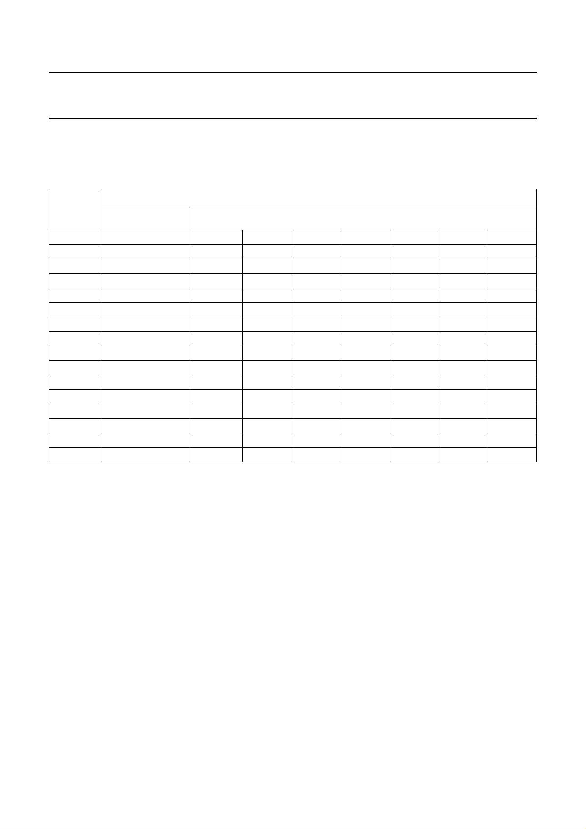
10.2 Memory mapping
The memory map of the 80C51 is shown in Fig.8.
In addition to all the SFRs, the microcontroller has
128 bytes of directly addressable (DATA) memory,
128 bytes of indirectly addressable (IDATA) memory and
512 bytes of AUX RAM, the on-chip ‘MOVX’ addressable
(XDATA) memory. On-chip XDATA memory access can
be disabledby settingthe ARD bit inPCON tologic 1. The
internal32-kbyte ROMof microcontrollerprogram (CODE)
memory can be accessed when EA is set to logic 1.
Via Ports P0, MA, P2 and P4it is possible toaccess up to
512 kbytes of external speech data memory stored in a
parallel flash memory. A CAD flash memory can also be
mappedin thisarea. Aserial(SPI orMicrowire compatible)
flash memory can be connected to P4 which is controlled
by theMCB. Up to 64 kbytes ofprogram (CODE) memory
can beconnected to the P0, P2and PSEN pads.This can
be any external program memory (like the MON51 target
debug ROM) if EA is logic 0.
When the EAMSFR bit (P4CFG.5) is logic 0(default after
reset), the XRAM-mapped control registers can only be
accessed if P4.3 is logic 1. Otherwise, XRAM addressing
is independent of the value of the P4.3 SFR bit.
2001 Apr 17 20
Page 21
Philips Semiconductors Product specification
Digital telephone answering machine chip PCD6001
handbook, full pagewidth
TICB
O PAD
DIS_XTAL
O PAD
MRST
I PAD
RST_ANA
I PAD
RST_IN
MRST
SPCON[7]
µC_CLK
osc_off
MODE
CONTROL
RAMIF
FS_event
RTC_event
TIME_event
DSP_event
TICBIF
CD
µCMS 80C51 CORE
CPU
XMEMU
MSEL
SF
GROUP INT.
TIMER 0
TIMER 1
PCON.0
to
PCON.1
INT15L2
ROMIF
pad_ale
pad_ea_n
IRQ1/IX1
DSP_req
2
I
C-bus_int
ARD
GROUP
WDRST
APPLICATION
SPECIFIC
FUNCTIONS
TICB
ANA
EX0 to EX6
DSP
I2C-BUS
PCON.2
to
PCON.7
PORT1
IF
WD
ANALOG
FUNCTIONS
DSP
I/O PADS
P1, P3
RD,WR
MSK_INT
SRAM
MAIN/AUX
RAM
256/512
BYTES
I/O PADS
EXTERNAL
64-kbyte
SRAM
P0, P2
PSEN
EA
ALE
INTERNAL
32 KBYTE
ROM
DRAM
ARAM
Fig.7 Microcontroller (MS 80C51) architecture and environment.
2001 Apr 17 21
FLASH
MICROWIRE/
SPI
MSK
MCB
FLASH
PARALLEL
PORT3
PORT4
FLASH
CAD
I/O PADS
P4
FLASH
2
I
C-BUS
MGT432
Page 22
Philips Semiconductors Product specification
Digital telephone answering machine chip PCD6001
handbook, full pagewidth
255
XDATA-mapped registers
P4.3 = 1, EAM = 0, ARD = X
or ARD = 0, EAM = 1, EA = 1
Main RAM SFR
IDATA
Internal XDATA
518
515
ConfReg
512
AUX RAM
memory
P2
MA
64K
32K
External data
memory
XDATA
P4.3 = X
ARD = X
P4.3 = 0
ARD = 1
External program
memory
CODE
Internal ROM
CODE
128
48
ADDRESSABLE
32
REGISTER
BANKS 0 TO 3
0
DATA
BIT
SPACE
XDATA
ARD = 0
Fig.8 Microcontroller memory map.
2001 Apr 17 22
P4.3 = X
ARD = 1
EA = 1
EA = 1
MGT433
Page 23
Philips Semiconductors Product specification
Digital telephone answering machine chip PCD6001
10.3 SFR mapping
The SFRmapping for themicrocontroller is shownin Table 12. All SFRsand their resetstates are describedin Table 13.
Table 12 SFR mapping
SFR
ADDRESS
(HEX)
F8 to FF IP1
F0 to F7 B
ADDRESSABLE
(2)
(2)
E8 to EF IEN1
E0 to E7 ACC
D8 to DF S1CON
D0 to D7 PSW
(1)
(2)
(2)
(2)
(2)
SPECIAL FUNCTION REGISTERS 8 BITS EACH
ONLY BYTE ADDRESSABLE
− −−−−−WDT
(2)
− −−−−−WDTKEY
IX1 −−−−−−
− −−−−−−
S1STA
(2)(3)
S1DAT
(2)
S1ADR
(2)
−−−−
− −−−−−−
C8 to CF MCON MBUF MSTAT −−−−−
REFR
(2)
(2)
(3)
GPADC GPDAR SYMOD − DTCON
(2)
(4)
− TCTRL
(4)
PMTR2
(4)
− P4CFG
−−
CDVC1 CDVC2 CDTR1
(3)
DTM1
(2)
TL1
DPH
(3)
DTM2
(2)
TH0
(2)
−−−PCON
(3)
MTD0 MTD1 MTD2
TH1
(4)
(4)
CDTR2
C0 to C7 IRQ1 INTC GPADR
(2)
(2)
(2)
XWUD V
−−−−PMTR1
MCSC MCSD ALTP −−−−
B8 to BF IP0
B0 to B7 P3
A8 to AF IEN0
A0 to A7 −−DTM0
98 to 9F P4 SPCON CKCON RTCON − CDTR1
90 to 97 P1
88 to 8F TCON
80 to 87 − SP
(2)
(2)
− −−−−−−
(2)
TMOD
(2)
TL0
DPL
Notes
1. SFRs in this column are both bit and byte-addressable.
2. Complies to 80C51 family architecture specification.
3. These registers are read only (all other SFRs are read/write).
4. Reserved register, used for testing purposes. Writing of reserved or undocumented bits might lead to unexpected
behaviour of the device (see Section 10.8).
(4)
2001 Apr 17 23
Page 24

Philips Semiconductors Product specification
Digital telephone answering machine chip PCD6001
Table 13 Microcontroller register list
NAME ADDRESS (HEX) DESCRIPTION RESET STATE
ACC E0 accumulator 0000 0000
ALTP AB LE and GPC control X000 0000
A − accumulator 0000 0000
B F0 B register for multiply, divide or scratch 0000 0000
CKCON 9A Clock Control Register 0000 0000
CDVC1 BB CODEC digital volume control for CODEC1 00XX 0XXX
CDVC2 BC CODEC digital volume control for CODEC2 00XX 0XXX
CDTR1 BD CODEC Test Register 1; see note 1 00XX 0XXX
CDTR2 B7 CODEC Test Register 2; see note 2 00XX 0XXX
DTCON C7 line selection and alternative gain control register XX00 X00X
DPL 82 data pointer low 0000 0000
DPH 83 data pointer high 0000 0000
DTM0 A2 DSP to Microcontroller Communication Register 0 (read only) 0000 0000
DTM1 A3 DSP to Microcontroller Communication Register 1 (read only) 0000 0000
DTM2 A4 DSP to Microcontroller Communication Register 2 (read only) 0000 0000
GPADC C3 automatic analog-to-digital conversion, channel select, request
confirm
GPADR C2 digital value of analog input (read only) 0000 0000
GPDAR C4 digital value of analog output 1000 0000
IEN0 A8 Interrupt Enable Register 0 0000 0000
IEN1 E8 Interrupt Enable Register 1 0000 0000
INTC C1 Interrupt Control Register XXXX XX00
IP0 B8 Interrupt Priority Register 0 X000 0000
IP1 F8 Interrupt Priority Register 1 0000 0000
IRQ1 C0 Interrupt Request Flag Register 0000 0000
IX1 E9 Interrupt Polarity Register XXX0 0000
MCSD AA Memory Control Serial Data Register 0000 0000
MCSC A9 Memory Control Serial Command Register XXXX 0000
MTD0 A5 microcontroller to DSP communication register 0 0000 0000
MTD1 A6 microcontroller to DSP communication register 1 0000 0000
MTD2 A7 microcontroller to DSP communication register 2 0000 0000
MCON C8 MSK Control Register 0000 0000
MBUF C9 MSK Data Buffer Register XXXX XXXX
MSTAT CA MSK Status Register 0X00 0000
P1 90 general purpose digital I/O 1111 1111
P3 B0 general purpose digital I/O 1111 1111
P4 98 P4 can be used to control flash memory XX01 1110
P4CFG 9F P4 configuration and addressing mode register 0000 0000
PCON 87 Power and Interrupt Control Register X000 0000
PMTR1 B5 Power Management Test Register 1; see note 2 0000 0000
XXXX X000
(1)
2001 Apr 17 24
Page 25

Philips Semiconductors Product specification
Digital telephone answering machine chip PCD6001
NAME ADDRESS (HEX) DESCRIPTION RESET STATE
PMTR2 B6 Power Management Test Register 2; see note 2 0000 0000
PSW D0 Program Status Word 0000 0000
RTCON 9B Real-Time Clock control 0000 0000
S1CON D8 I
S1ADR DB I
S1DAT DA I
S1STA D9 I
2
C-bus Serial Control Register 0000 0000
2
C-bus own slave address register 0000 0000
2
C-bus Data Shift Register 0000 0000
2
C-bus Status Register (read only) 1111 1000
SYMOD C5 analog system mode control 0000 0000
SPCON 99 system power and clock configuration 0XX0 0000
SP 81 Stack Pointer 0000 0111
TCON 88 Timer/counter Control Register 0000 0000
TMOD 89 Timer/counter Mode Control Register 0000 0000
TL0 90 Timer Low Register 0 0000 0000
TL1 91 Timer Low Register 1 0000 0000
TH0 92 Timer High Register 0 0000 0000
TH1 93 Timer High Register 1 0000 0000
VREFR BA Voltage Reference Register 1010 0000
WDT FF Watchdog Timer 0000 0000
WDTKEY F7 Watchdog Key Register 0000 0000
XWUD B9 external wake-up disable 0000 0000
(1)
Notes
1. All SFR bitswith reset state ‘X’ are either‘spare’ (i.e. have a memorybit in this position withreset state ‘0’) or‘-’(i.e.
do not haveaphysical memory bit in this position).All ‘spare’ bits can be addressedand used as additional general
purpose bits. All bits marked ‘-’ cannot be addressed by the user. To see which bits are ‘spare’ or ‘-’ refer to the
respective SFR layouts.
2. Reserved registers, used for testing purposes. Writing of undocumented or reserved bits might lead to unexpected
behaviour of the device (see Section 10.8).
2001 Apr 17 25
Page 26

Philips Semiconductors Product specification
Digital telephone answering machine chip PCD6001
10.4 Microcontroller interrupts
The microcontroller has 15 interrupt sources, shown
below, which can be programmed to have a low or high
priority. If enabled these interrupts sources result in jump
to the addresses shown in Table 14.
• EX2 to EX6 asynchronous external interrupts via
P1.0 to P1.4
• EX0 and EX1 asynchronous external interrupts via
P3.2 (INT0N) and P3.3 (INT1N)
• DSP_event
• FS_event
• TIME_event
• I2C-bus interrupt
• RTC_event
• Timer 0 and Timer 1 interrupt
• MSK interrupt.
The external interrupt configuration of P1 is shown in
Fig.9. Pins P1.5, P1.6 and P1.7 cannot be used as
externalinterrupts. The IX1SFR determinesthe polarityof
the external interrupt sources of P1. Clearing the ‘global
enable’ bit in IEN0 disables all interrupt sources. Using
IEN0 (and IEN1) each individual external interrupt can be
enabled or disabled.
The IRQ1 SFR stores all external interrupts. So if an
external interrupt with a low priority is detected during
execution ofanother (highor lowpriority) interrupt itwill be
handled just after the return of this interrupt.
The interrupt serviceroutine for an externalinterrupt must
clear theright IRQ1 flag toindicate that it hasserviced the
interrupt request. Notice that during the interrupt routine
this flag can be set again immediately after clearing the
IRQ1 flag if the interrupt source is (still) HIGH.
The complete interrupt system is shown in Fig.10. All
15 interrupts are allocated and canbe given a low or high
priority according to the setting of IP0 and IP1.
Each interrupt source can be individually enabled by
means of IEN0 and IEN1.
The IRQ1 and IX.7 registersare clocked (a clock which is
active during Idle) and can be set by P1.0 to P1.4, the
TIME_event, the DSP_event, the FS_event and the
RTC_event. These flags canonly be cleared by software.
Only TCON.1, TCON.3, TCON.5 and TCON.7 flags are
cleared bythe interrupt controllerhardware. All otherflags
must be cleared by software.
The pollingof apotential interrupt goesfrom ahigh priority
to a low priority interrupt. Within a high (or low) priority
interrupt level the EX0(if set to high priority) will be polled
first followed by the next high priority interrupt.
Theinterrupt SFRsIP0, IP1,IEN0,IEN1, IRQ1andIX1 are
defined inSections 10.4.1 to 10.4.6. A flagset tologic 1 in
IP0 or IP1 (Tables 15 and 16) causes the corresponding
interrupt to have high priority.
2001 Apr 17 26
Page 27

Philips Semiconductors Product specification
Digital telephone answering machine chip PCD6001
Table 14 Allocation of interrupt sources
VECTOR SOURCE NUMBER
(1)
PRIORITY
0003 EX0 0 1 external interrupt 0 IEN0.0/IP0.0
000B T0 1 4 Timer 0 interrupt IEN0.1/IP0.1
0013 EX1 2 7 external interrupt 1 IEN0.2/IP0.2
001B T1 3 10 Timer 1 interrupt IEN0.3/IP0.3
0023 MSK_event 4 13 MSK RI or TI interrupt IEN0.4/IP0.4
002B TIME_event 5 2 TIME interrupt IEN0.5/IP0.5
0033 FS_event 6 5 FS interrupt IEN0.6/IP0.6
003B EX2 7 8 external interrupt 2 IEN1.0/IP1.0
0043 EX3 8 11 external interrupt 3 IEN1.1/IP1.1
004B EX4 9 14 external interrupt 4 IEN1.2/IP1.2
0053 EX5 10 3 external interrupt 5 IEN1.3/IP1.3
005B EX6 11 6 external interrupt 6 IEN1.4/IP1.4
0063 I
2
C-bus 12 9 I2C-bus interrupt IEN1.5/IP1.5
006B DSP_event 13 12 DSP interrupt IEN1.6/IP1.6
0073 RTC_event 14 15 RTC interrupt IEN1.7/IP1.7
(2)
DESCRIPTION IENx/IPx
Notes
1. For some C-compilers ‘1’ has to be added to this number.
2. The interrupt controller supports up to 15 interrupt sources, each with a 2-level (high or low) priority. High priority
interrupt is always serviced before a low priority interrupt, but within the high and low levels, interruptsare serviced
in the order shown in this column.
handbook, full pagewidth
P1.7
P1.6
P1.5
P1.4
P1.3
P1.2
P1.1
P1.0
RTC_event
DSP_event
TIME_event
RTC
FS
TIME
EX6
EX5
EX4
EX3
EX2
IX1 IEN1
Fig.9 Port 1 external interrupt configuration.
2001 Apr 17 27
IRQ1
MGM773
Page 28
Philips Semiconductors Product specification
Digital telephone answering machine chip PCD6001
handbook, full pagewidth
EXP1N + XWU
SOURCE
EX0
T0
EX1
T1
MSK
2
I
C-BUS
FS_event
EX2
EX3
EX4
EX5
EX6
TIME_event
DSP_event
RTC_event
IX.0
IX.1
IX.2
IX.3
IX.4
EDGE/LEVEL
TCON.0 TCON.1 IEN0.0
TCON.2
POLARITY
FLAGS ENABLE
TCON.5
TCON.3
TCON.7
MSTAT.0
MSTAT.1
S1CON.3
INTC.0
IRQ1.0
IRQ1.1
IRQ1.2
IRQ1.3
IRQ1.4
IRQ1.5
IRQ1.6
IRQ1.7
IEN0.1
IEN0.2
IEN0.3
IEN0.4
IEN0.5
IEN0.6
IEN1.0
IEN1.1
IEN1.2
IEN1.3
IEN1.4
IEN1.5
IEN1.6
IEN1.7
PRIORITY
IP0.0
IP0.1
IP0.2
IP0.3
IP0.4
IP0.5
IP0.6
IP1.0
IP1.1
IP1.2
IP1.3
IP1.4
IP1.5
IP1.6
IP1.7
INTERRUPT
SCANNING
INTERRUPT CONTROLLER
MGM774
XWUD
XWUD.0
to
XWUD.7
EXP1N
clocks
Fig.10 PCD6001/80C51 interrupt system.
10.4.1 INTERRUPT PRIORITY REGISTER 0 (IP0)
Table 15 Interrupt Priority Register 0 (SFR address B8H); reset state 00H
76 543210
−priority FS_event priority TIME priority MSK priority T1 priority EX1 priority T0 priority EX0
10.4.2 Interrupt Priority Register 1 (IP1)
Table 16 Interrupt Priority Register 1 (SFR address F8H); reset state 00H
76543210
priority RTC priority DSP priority I2C priority EX6 priority EX5 priority EX4 priority EX3 priority EX2
2001 Apr 17 28
Page 29

Philips Semiconductors Product specification
Digital telephone answering machine chip PCD6001
10.4.3 INTERRUPT ENABLE REGISTER 0 (IEN0)
Table 17 Interrupt Enable Register 0 (SFR address A8H); reset state 00H
76543210
global
enable
enable
FS_event
enable TIME enable
MSK_event
enable T1 enable EX1 enable T0 enable EX0
10.4.4 I
NTERRUPT ENABLE REGISTER 1 (IEN1)
Table 18 Interrupt Enable Register 1 (SFR address E8H); reset state 00H
76543210
2
enable RTC enable DSP enable I
10.4.5 I
NTERRUPT REQUEST FLAG REGISTER (IRQ1)
C enable EX6 enable EX5 enable EX4 enable EX3 enable EX2
Table 19 Interrupt Request Flag Register 1 (SFR address C0H); reset state 00H; note 1
76543210
RTC flag DSP flag TIME flag EX6 flag EX5 flag EX4 flag EX3 flag EX2 flag
Note
1. The flags of IRQ1 will be set to logic 1 by hardware if the interrupt occurs. They must be cleared by software in the
interrupt service routine.
10.4.6 I
NTERRUPT POLARITY REGISTER (IX1)
Table 20 Interrupt Polarity Register (SFR address E9H); reset state 00H; note 1
76543210
spare spare spare polarity EX6 polarity EX5 polarity EX4 polarity EX3 polarity EX2
Note
1. A polarity bit set to logic 1 in IX1 will cause the external interrupt to be active HIGH.
10.4.7 I
NTERRUPT CONTROL REGISTER (INTC)
Table 21 Interrupt Control Register (SFR address C1H); reset state 00H
76543210
spare spare spare spare spare spare extended
FS flag
wake-up;
XWU
10.4.8 E
XTERNAL WAKE-UP DISABLE REGISTER (XWUD)
Table 22 External Wake-up Disable Register (SFR address B9H); reset state 00H
76543210
RTC XWU
disable
DSP XWU
disable
TIME XWU
disable
EX6 XWU
disable
EX5 XWU
disable
EX4 XWU
disable
EX3 XWU
disable
EX2 XWU
disable
2001 Apr 17 29
Page 30

Philips Semiconductors Product specification
Digital telephone answering machine chip PCD6001
10.5 Interface to DSP
TheDSP toMicrocontrollerInterface (DMI)can beusedfor
the following purposes:
• Transferring compressed speech data from
microcontroller to DSP
• Transferring compressed speech data from DSP to
microcontroller
• Transferring DSP parameters (DSP mode, tone
frequency etc.) from microcontroller (API) to the DSP
• Transferring DSP events (Caller ID, Ring Detect, VOX,
Call Progress etc.) to the microcontroller.
The microcontroller and the DSP can communicate by
means of 6 SFRs (MTD0, MTD1 and MTD2 and DTM0,
DTM1 and DTM2) and 4 DSP I/O registers (DTMC,
DTMD, MTDC and MTDD), see Fig.11. The DTMC and
MTDC registers are used for communication and control
and the DTMD and MTDD registers for transferring data.
TheMicro Transmit (MT),DR (DSPreceive) andDT (DSP
Transmit), Micro Receive (MR) ensure that either the old
data is read or new data is read although the DSP and
microcontroller operate on different clocks. This can be
achieved bymeans of simplehandshake circuitry in either
direction. TheDR state machineensures that theDSP will
never readnew MTDCcontrol data andold MTDDspeech
data. In order to guarantee proper transitions of the
DR state machine the DSPalwayshas to read the DTMC
first and afterwards the DTMD IO register.
The TICB generates the DSP_event interrupt when it
receives a dsp_uc_req signal.The dsp_uc_req cannot be
generated by the microcontroller because the dsp_event
interrupt mustbe able towake-up the microcontroller from
Power-down.
MTD0/1/2 are written by the microcontroller. After each
write toMTD0 the contentsof MTD0/1/2 aretransferred to
the 16-bitregisterMTDD and the 8-bitregister MTDC (the
MSB is setto 00H), which can be readby the DSP via the
DSP I/O bus. In this way the DSPalwaysreceives a valid
controlbyteandavalid16-bitdata word.If MTD0is written
while the DSP is turned off the MTD0 value will be
transferred tothe MTDCIO-register assoon as theDSP is
turned on.
The MTDC and MTDD registers are continuously and
immediately read by the DSP after every FS1 interrupt.
The microcontroller canwrite a newword to MTD0/1/2but
has to waitfor at least 125 µs to besure that the DSP has
read the previous value.
DTM0/1/2 are read by the microcontroller as SFRs. The
contents ofthe DTMDand DTMCregisters aretransferred
to the DTM0/1/2 SFRs when the DSP writes the DTMC
register. At this time an interrupt signal called DSP_event
is generated to the microcontroller, which triggers the
microcontroller to read the DTM0/1/2 SFRs. In this way
DSP events and speech data can be transferred easily to
the microcontroller. The DSP will transfer a maximum of
3 bytes, one command byte and two data bytes, for
example; every 125 µs to the microcontroller. Thus one
write to DTMC takes place every 125 µs.
Similarly, the microcontroller can transfer a maximum of
3 bytes every 125 µsto the DSP. Thusone write to MTD0
takes place every 125 µs. The default rate for the
FS_eventinterrupt willbe FS1/8resultingin adata transfer
rate of 10 words every 10 ms which equals 16 kbits/s.
In caseahigher rateis neededthe FS_eventinterrupt rate
can be switched to FS1/4.
10.6 Interface to Real-Time Clock (RTC)
When theRTC_eventinterrupt is enabled inIEN1 and the
‘global enable’ bit inIEN0 isset and thePCD6001 isnot in
Emergency mode (CKCON.7 = 1),themicrocontroller will
get an RTC_event interrupt every 1 minute. The RTC
interrupt service routine must clear the RTC flag. The
RTC_event interrupt will also wake-upthe microcontroller
when it is in the Power-down or in the Idle state. Under
powersaving conditionsthis willallowthe usertoswitch off
the microcontrollerand still maintain anaccurate real time
clock.
2001 Apr 17 30
Page 31

Philips Semiconductors Product specification
Digital telephone answering machine chip PCD6001
handbook, full pagewidth
dsp_clk
FS1
interrupt
RD16010
DTMC write
IO
DT
DTMC
LSB
DTMD
LSB
MSB
MTDD
LSB
MSB
MTDC
LSB
TICB
dsp_µc_req
µc_dsp_ack
DTM0
DTM1
DTM2
MTD1
MTD2
MTD0
dsp_µc_req
MR
µC_CLK
DSP_event
DTM0,
DTM1 or DTM2
SFR
µCMS 80C51
FS_event
MICRO-
CONTROLLER
80C51
rd_MTDD
rd_MTDC
MTDC/D write
DR
dsp_µc_ack
µc_dsp_req
DSP
Fig.11 DSP to Microcontroller Interface (DMI).
2001 Apr 17 31
MT
MTD0 write
MGM775
Page 32

Philips Semiconductors Product specification
Digital telephone answering machine chip PCD6001
10.7 Interface to the Memory Control Block (MCB)
The MCB is a3-wireserial interface designed to interface
with a versatile range of serial flash memories (both
Microwire and SPI mode 0/3 compatibleslave devices) in
parallel with program OTP/external ROM and even
external data SRAM.
The 3-wire serial interface consists of a serial data output
(FSO) serial data input (FSI) and a serial clock signal
(FSK). FSK, FSO and FSI are alternative functions of the
general purpose I/O pins P4.1, P4.2 and P4.4. The serial
interfaceis controlledviathe MCSCand MCSDSFRs.The
FSK and FSO outputs are both open-drain and must be
pulled to 3 V with external resistors R
FSK
and R
FSO
. The
recommended valuefor bothresistors athigh FSKspeeds
(>1 MHz) is 1 kΩ. The MCSC SFR is defined in
Section 10.7.1.
Turning the MCBon by setting bitMCSC.3,will switch the
FSK and FSO pins to logic 0. A write to MCSD will
generate the appropriate FSK/FSO signal. A read from
MCSD willonly generate 8 FSKpulses and willshift-in the
next byte. The shifting and the FSK/FSO signal can be
suppressed bysetting bit 2of MCSC. Thiscan beused for
reading the last byteout of the serial flash memory during
a read sequence. The FSK shift off operation however is
not necessary if the MCB is already turned off when
reading the MCSD SFR for the last time.
If a serial flash memory is chosen the FSK master clock
rate can be selected with bits 0 and 1, as shown in
Table 24. The MCB is always master, which means that
the FSK clock is always generated by the PCD6001.
Dependingon theFSK clockrate, theshifting cancontinue
for8 × 32 microcontroller_CLKperiods. Duringthis period,
the microcontroller should not be put in a power saving
mode (Idle, Power-down and System-off), otherwise the
shifting will stop.
Data coming from or goingto the serial flash memory can
be accessed by means of the MCSD SFR. This is simply
an 8-bit serialshift register. The first FSOand FSI bits are
always themost significant bits ofMCSD. The first readof
the MCSD SFR willonly serially load the MCSD SFR with
valid data. Therefore,the first read operationmust always
be followed with another read operation which reads the
actual received data out of the MCSD SFR.
The serial shifting of bits into and out of MCSD is done at
the same moment: 1 microcontroller clock before the
falling edge of FSK (tSF). When the FSK speed is
programmedat thehighestspeed (microcontroller_CLK/4)
this shifting will be done in the middle of the FSK HIGH
level time. The most time-critical situation is when FSK is
only 2 clocks wide and has a frequency of 3.5 MHz
(14 MHz/4). In this case make sure that t
be controlledby the valueof R
, isgreater than thehold
FSK
r(FSK)
, which can
time requirement of the slave device.
Figure 12 shows how a Microwire compatible device can
beaccessed withan FSKspeed ofmicrocontroller_CLK/4.
A SPI mode 0/3 device requires an additional FSK clock
falling edge to trigger the slave device to generate valid
data on the FSI line. The SPImode 3can be achieved by
starting with FSK high when the device is turned on (turn
MCBon afterasserting thechipenable oftheslave device)
and byending withFSK. TheSPI mode 0 canbe achieved
bygenerating anadditional FSKpulse(by turningthe MCB
off and on again, see Fig.12) between the last write to
MCSD and the first read of MCSD.
A variety of serial flash memorydriversoftware packages
is included in the API software for the microcontroller that
is provided with the chip.
An application note is available to help implementation of
the software for the SPI.
10.7.1 MEMORY CONTROL SERIAL COMMAND REGISTER (MCSC)
Table 23 Memory Control Serial Command Register (SFR address A9H)
76543210
spare spare spare spare MCB on shift off FSK rate 1 FSK rate 0
Table 24 Selection of FSK clock rate
MCSC.1 MCSC.0 FSK CLOCK RATE
0 0 microcontroller_CLK/4
0 1 microcontroller_CLK/8
1 0 microcontroller_CLK/16
1 1 microcontroller_CLK/32
2001 Apr 17 32
Page 33

Philips Semiconductors Product specification
Digital telephone answering machine chip PCD6001
handbook, full pagewidth
FSO
FSI
FSK
FSO
FSI
FSK
slave shift in
t
h(FSO)
O7
MCBONMCSD
WRITE
t
r(FSO)
DATA OUT
t
su(FSO)
DATA IN
MCSD
READ
O3O6
t
r(FSK)
MCB
SHIFT OFF
O2 O1 O0O5 O4
T
FSK
MCSD
READ
slave shift out slave shift out
MCB
OFF
I7 I6
t
su(FSI)
t
V(FSI)
MGM776
t
h(FSI)
Fig.12 MCB timing for a Microwire compatible device.
Table 25 MCB timing
SYMBOL PARAMETER VALUE
T
FSK
t
su(FSO)
t
h(FSO)
t
r(FSK)
t
r(FSO)
t
su(FSI)
t
h(FSI)
t
V(FSI)
FSK period N × t
micro_clock
FSO setup time with respect to the rising edge of FSK (N/2 + 1) × t
FSO hold time with respect to the rising edge of FSK (N/2 − 1) × t
FSK rise time note 2
FSO rise time note 2
FSI setup time with respect to the internal shift clock (N/2 + 1) × t
FSI hold time with respect to the internal shift clock >t
micro_clock
FSI valid time with respect to the falling edge of FSK depending on the used flash memory
; note 1
micro_clock
micro_clock
micro_clock
− t
− t
− t
r(FSO)
r(FSK)
V(FSI)
Notes
1. N depends on the chosen FSK clock rate and can be 4, 8, 16 and 32.
2. The rise time of FSK and FSO depends on the externally connected pull-up resistor and the capacitive load.
2001 Apr 17 33
Page 34

Philips Semiconductors Product specification
Digital telephone answering machine chip PCD6001
10.7.2 PARALLEL FLASH INTERFACE
If a parallel (4-Mbit) flash memory is chosen Table 26 is
valid.
Table 26 Using P4 with 4-Mbit parallel flash memory
P4.2 P4.1 P4.0 ADDRESS
0 0 0 Bank 0: 00000H to 0FFFFH
0 0 1 Bank 1: 10000H to 1FFFFH
0 1 0 Bank 2: 20000H to 2FFFFH
0 1 1 Bank 3: 30000H to 3FFFFH
1 0 0 Bank 4: 40000H to 4FFFFH
1 0 1 Bank 5: 50000H to 5FFFFH
1 1 0 Bank 6: 60000H to 6FFFFH
1 1 1 Bank 7: 70000H to 7FFFFH
Since parallelflash memoryhas a muchlarger addressing
range than the 64 kbytes addressing capability of the
80CL51, additional addressing is done by means of the
P4 SFR and the P4 I/O pad. The P4 SFR is connected to
Port P4 as shown in Table 27.
One pin is necessary to enable and disable the flash
memory to reduce power consumption. Four pins of P4
are necessaryto connect various typesof flash memories:
• A parallel flash: P4.0 to P4.2, P4.3, RD and WR are
connected to MA[16:18], CEN, OEN and WN
• A serial flash: FSO, FSI, FSC and P4.3 are connected
to DI, DO, SK and CEN pins
• A CAD flash: P4.1 to P4.3, RD, WR are connected to
CLE, ALE, CEN, REN and WEN pins.
RD andWR are availableas separatepins. If an accessis
done to the AUX RAM (ARD bit of PCON equals logic 0)
the RD and WR will be logic 1 on these pins.
Bits 1, 2and 4 ofPort 4 areset toFSI,FSKandFSO when
a serial flash is selected in the MCSC SFR.
The P4SFRis definedin Table 28.Bits P4.6 and P4.7are
not available as addressable bits or port pins.
P4 pin behaviour and configuration is described in more
detail in Section 16.2.
Table 27 P4 pin behaviour (alternative pin functions)
765
−−P4.5/GPC P4.4/FSI P4.3 P4.2/FSO P4.1/FSK P4.0/LE
Note
1. The alternative outputs (GPC, FSI, FSO,FSKand LE) are connected with the general purpose outputs via an AND
logic gate. Therefore when using the alternative functions the corresponding port bits have to be set to a logic 1.
(1)
43210
10.7.2.1 Port 4 Register (P4)
Table 28 Port 4 Register (SFR address 98H); reset state 1EH
76543210
P4.7 P4.6 P4.5 P4.4 P4.3 P4.2 P4.1 P4.0
2001 Apr 17 34
Page 35

Philips Semiconductors Product specification
Digital telephone answering machine chip PCD6001
10.8 The test registers CDTRx, PMTRx and TCTRL
The special function registers CDTR1, CDTR2, PMTR1, PMTR2 and TCTRL can puttheDSP or CODECs into various
test modes. In these test modes normal operation is not guaranteed. The output behaviour of P3 can be changed and
the DSP test modes can lead to a higher current consumption and to malfunction of the DSP. Three bits however are
accessible by the user: CDTR2.0, PMTR2.0 and PMTR2.2. See Tables 29 and 30 for detailed description.
Table 29 CDTR2 (98H) bit assignment; reset state 00H
76543 2 10
reserved reserved reserved reserved reserved reserved reserved avo_off
Table 30 PMTR2 (98H) bit assignment; reset state 00H
76543 2 10
(2)
reserved reserved reserved reserved reserved atc_chop_en
reserved avb_off
Notes
1. For minimum current consumption in POTS mode (telephone line supplied operation), two bits of these registers
have to be set (PMTR2.0 = 1, CDTR2.0 = 1).
2. For best noise performance of the Sigma Delta AD, chopping has to be enabled (PMTR2.2 = 1).
(1)
(1)
10.9 Interface to Timing and Control Block (TICB)
The interface to the TICB consists of the special function registers SPCON, CKCON and RTCON and the signals
microcontroller_CLK_EN, microcontroller_CLK, FS_event, Time_event and RTC_event. The signals are described in
Section 10.1.
10.10 Power and Interrupt Control Register (PCON)
Table 31 Power and Interrupt Control Register (SFR address 87H); reset state 00H
76543 2 10
spare ARD spare WLE/EW GF1 GF0 PD IDL
Table 32 Description of PCON bits
BIT SYMBOL DESCRIPTION
7 − Spare, may be used as general purpose bit.
6 ARD AUX-RAM Disable. If ARD = 1, then theaccess of a MOVX instruction to the512 bytes
of the AUX-RAM is disabled. If ARD = 1, then a MOVX operation can access the lower
512 bytes of the external memory. The upper part of the external memory can always
be accessed independently of the setting of the ARD bit.
5 − Spare, may be used as general purpose bit.
4 WLE/EW Watchdog Load Enable. This flag must be set by software prior to loading the
Watchdog Timer. The flag is reset when the timer is loaded. See Section 10.10.3
3 GF1 General Purpose Flag 1.
2 GF0 General Purpose Flag 0.
1PDPower-down mode select. Setting this bit activates the Power-down mode; see
Section 10.10.2.
0 IDL Idle mode select. Setting this bit activates the Idle mode; see Section 10.10.2.
2001 Apr 17 35
Page 36

Philips Semiconductors Product specification
Digital telephone answering machine chip PCD6001
10.10.1 IDLE MODE
In the Idle state Timer 0 and Timer 1 and the I2C-bus
controller are still clocked. The CPU status along with all
SFRs, main RAM and AUX RAMregisters are preserved.
Leaving the Idle state can be done by any enabled
interrupt or reset. The microcontroller hardware will clear
the Idle flag and start executing the interrupt. When the
interrupt is serviced (RETI instruction) the microcontroller
will execute the next instruction following the instruction
that put the microcontroller in the idle state.
10.10.2 POWER-DOWN MODE
In the Power-down state the clock of the entire
microcontroller with its peripherals is off. The CPU status
along with all SFRs, main RAM and AUX RAM registers
arepreserved. Leavingthe Power-downstate canbedone
by any active enabled interrupt source or reset.
The microcontroller hardware will clear the PD flag and
startexecuting theinterrupt. Whenthe interruptis serviced
(RETI instruction) the microcontroller will execute the
instruction following the instruction that put the
microcontroller in the PD state.
Toggling of the ALE signal (for enhanced EMC
performance) is not supported.
10.10.3 THE WATCHDOG CIRCUITRY
Thepurpose ofthe watchdogisto resetthe microcontroller
if it enters erroneous states caused by EMI or bugs in the
software that cannot be detected or eliminated.
When enabledthe watchdog circuitrywill generate areset
if the user program fails to reload the Watchdog Timer
within a specified length of time known as the watchdog
interval.
The watchdog interval is calculated as follows:
T
The programmer should implement the following protocol:
1. Write the key value 55H to the WDTKEY SFR to
2. Set the WLE/EW bit to logic 1 to initially enable the
3. Enable the Watchdog Timer by writing a value not
4. Enable the load of the WDT SFR by setting the WLE
5. Load the watchdog interval by writing the required
6. Write avalue notequal to 55Hto theWDTKEY SFRto
7. Repeat steps 4 and 5 in the user software before the
Note in Metalinkemulation mode the watchdog cannot be
used, the watchdog reset will reset the entire chip.
256 WDT–()
WD
disable the watchdog.
watchdog. WLE/EWnow functions as aWLE bit. Only
a reset can clear the EW bit.
equal to 55H to the WDTKEY SFR. This is only
necessary if the previous value of the WDTKEY
register was 55H. The value after reset is 00H.
bit to logic 1.
value into the WDTSFR. After the load the WLEbitis
set to logic 0 again by the watchdog hardware. The
value of WDT is 00H after reset.
enable the watchdog.
Watchdog Timer expires.
×=
12287
-----------------------------------------------------microcontroller_CLK
2001 Apr 17 36
Page 37

Philips Semiconductors Product specification
Digital telephone answering machine chip PCD6001
2
The I
10.11 I2C-bus
The serial portI2C-bus is asimple bidirectional 2-wire bus
for efficient inter IC data exchange. The I2C-bus consists
of a data line (SDA) and a clock line (SCL). These lines
also function as I/O Port P1.7 and P1.6 respectively.
The system is unique because data transport, clock
generation, addressrecognition and busarbitrationare all
controlled by hardware. The I2C-bus serial I/O has
complete autonomy in byte handling andsupports all four
I2C-bus operating modes:
• Master transmitter
• Master receiver
• Slave transmitter
• Slave receiver.
C-bus block contains 4 SFRregisters.The mode of
operation is controlled by the S1CON register. S1STA is
the status register whosecontents may also be used as a
vector to various serviceroutines.S1DAT is the data shift
register and S1ADR is the slave address register. Slave
address recognition is performed by hardware.
An application note is available to help implementation of
the software for the I2C-bus.
handbook, full pagewidth
SDA
BUS ARBITRATION LOGIC
SCL
S1ADR
OWN ADDRESS REGISTER
S1DAT
DATA SHIFT REGISTER
BUS CLOCK GENERATOR
SERIAL CONTROL REGISTER
S1CON
S1STA
STATUS REGISTER
Fig.13 I2C-bus serial I/O.
MICROCONTROLLER ASF GROUP INTERFACE
MGM777
2001 Apr 17 37
Page 38

Philips Semiconductors Product specification
Digital telephone answering machine chip PCD6001
10.11.1 SERIAL CONTROL REGISTER (S1CON)
Two bits are affected by the I2C-bus hardware, the SI bit is set to logic 1 when a serial interrupt is requested, and the
STO bit is set to logic 0 (cleared) when a STOP condition is present on the I2C-bus. The STO bit is also cleared when
ENS1 = 0. When the I2C-bus block is in the Master mode theserial clock frequency is determined by the clock rate bits
CR[2:0].
Table 33 Serial Control Register (SFR address D8H)
76543210
CR2 ENS1 STA STO SI AA CR1 CR0
Table 34 Description of S1CON bits
BIT SYMBOL DESCRIPTION
7 CR2 Clock rate. This bit along withbits CR1 and CR0 determines the serial clock frequency
6 ENS1 When this bit is set to logic 0 the I
5STAStart flag. When the STA bit is set to logic 1 in Slave mode, the I
4STOStop flag. With this bit set to logic 1 while in Master mode a STOP condition is
3SII
2AAAssert Acknowledge. When set to logic 1 an acknowledge will be returned during the
1 CR1 Clock rate. These 2 bits along with the CR2 bit determine the serial clock frequency
0 CR0
2
when I
C-bus is in Master mode, see Table 35.
2
C-bus is disabled, outputs SDA and SCL are in the
high-impedance state, and P1.6 and P1.7 function as open-drain ports. With this bit set
to logic 1 the I2C-bus is enabled. The P1.6 and P1.7 port latch must be set to logic 1.
2
C-bus hardware
checks the status of the I2C-bus and generates a START condition if the bus is free. If
STA is set to logic 1 while the I2C-bus is in Master mode, the I2C-bus transmits a
repeated START condition.
2
generated. When aSTOP condition is detectedon the bus, theI
C-bus hardwareclears
the STOflag. In the Slavemode, the STO flag mayalso be set to logic 1 to recover from
an error condition. In this case no STOP condition is transmitted to the I2C-bus.
However, the I2C-bus hardware behaves as if a STOP condition has been receivedand
releases SDA and SCL. The I2C-bus then switches to the ‘not addressed’ receiver
mode. The STO flag is automatically cleared by hardware.
2
C-bus interrupt flag. When this flag is settologic 1, an acknowledge is returned (i.e.
an interrupt is generated) after any one of the following conditions:
• A start condition is generated in Master mode
• Own slave address received during AA = 1
• General call address received while S1ADR[0] = 1and AA = 1
• Data byte received or transmitted in Master mode (even if arbitration is lost)
• Data byte received or transmitted as selected slave
• Stop or start condition received as selected slave receiver or transmitter.
acknowledge clock pulse on SCL when:
• Own slave address is received
• General call address is received while S1ADR[0] = 1
• Data byte is received while device is a selected slave.
With AA = 0 no acknowledge will be returned. Consequently, no interrupt is requested
when the ‘own slave address’ or general call address is received.
2
when I
C-bus is in Master mode, see Table 35.
2001 Apr 17 38
Page 39

Philips Semiconductors Product specification
Digital telephone answering machine chip PCD6001
Table 35 I2C-bus bit frequencies in Master mode
CR2 CR1 CR0
f
microcontroller_clk
DIVIDED BY
I2C-BUS BIT FREQUENCY (kHz) at f
0.9 MHz 3.58 MHz 7.16 MHz 14.32 MHz 21 MHz
microcontroller_clk
0 0 0 10 90 358 −−−
0 0 1 20 45 179 358 −−
0 1 0 30 30 119 239 −−
0 1 1 40 22 90 179 358 −
1 0 0 80 11 45 89.5 179 269
1 0 1 120 7.5 30 59.7 119 179
1 1 0 160 5.6 22 44.8 89.5 134
111 − −−−−−
Note thatany I2C-bus devicetolerates a maximumand sometimesa minimum SCLfrequency. The correctsetting ofbits
CR2, CR1 and CR0 using a specific microcontroller clock frequency is therefore important.
10.11.2 STATUS REGISTER (S1STA)
S1STA is an 8-bit read-only register. Its contents may be used as a vector to a service routine. This optimizes the
response time of the software and consequently the I2C-bus.
Table 36 Status Register (SFR address D9H); reset state F8H
BIT SYMBOL DESCRIPTION
7 to 3 SC[4:0] contains the status code defined by the I
2
C protocol
2to0 − not used, all bits are 0
10.11.3 DATA SHIFT REGISTER (S1DAT)
S1DAT containsthe serial data tobe transmitted ordata that has justbeen received. Bit 7 istransmitted or receivedfirst.
Table 37 Data Shift Register (SFR address DAH); reset state 00H
BIT SYMBOL DESCRIPTION
7 to 0 S1DAT[7:0] I2C-bus serial data
10.11.4 A
DDRESS REGISTER (S1ADR)
This 8-bit ‘own address register’ may be loaded with the 7-bit address to which the controller will respond when
programmed asaslave receiver/transmitter. The LSBbit GC is used todetermine whether the generalCALL address is
recognized.
Table 38 Address Register (SFR address DBH); reset state 00H
BIT SYMBOL DESCRIPTION
2
7 to 1 SLA[6:0] own I
C-bus address
0 GC 0: general CALL address is not recognized
1: general CALL address is recognized
2001 Apr 17 39
Page 40

Philips Semiconductors Product specification
Digital telephone answering machine chip PCD6001
10.12 MSK modem
The MSK modem is used for in-band signalling between
handset and base in analog cordless telephone systems
CT0, CT1 and CT1+. The MSK modems receiver and
transmitter can be enabled separately. Receive and
transmit interruptscan wake-up the microcontrollerduring
its power saving Idle mode. The baud rates are
programmable between 1200 and 4800 baud. Figure 14
shows the functional diagram of the MSK modem.
The MIN input is the alternative input of P3.7 and
MOUT[2:0] is the alternative output of P3.0, P3.1 and
P3.6.TheRX andTX mutecan bedone insoftware byany
pin of MA, P1, P3and P2. TheMTI and MRIinterrupts are
OR-ed togetherto a singleinterrupt calledmsk_int. So the
msk_in interrupt handler should investigate the status of
the MRI and MTI bit in the MCON SFR.
The MOUT[2:0] outputs and the MIN input are alternative
functions of P3.0, P3.1, P3.6 and P3.7. The MOUT[2 :0]
outputs are ‘111’ when the MSK transmitter is disabled
(default after reset).Therefore, P3.0, P3.1, P3.6 and P3.7
canstill beused asgeneral purposeI/O ports. Settingbit 7
of MSTAT will invert the MIN polarity.
The modem has the following features:
• Full-duplex operation via 8-bit parallel interface; the
message is fully Manchester coded/decoded
• Automatic detection of 16 bit Manchester preamble
pattern
• The last received 4 bits of the preamble pattern are
programmable
• Receiver full, transmitter empty indication bits
• Manchestercodinganddecodingforclockrecoveryand
early error detection
• Programmable input polarity
• Baud rate selection from 1200, 2400, 3600
and 4800 baud with internal modem timer
• Receiver and transmitter off-states with no power
consumption.
2001 Apr 17 40
Page 41

Philips Semiconductors Product specification
Digital telephone answering machine chip PCD6001
handbook, full pagewidth
MREN
80C51 CORE
MSK_INT
MRI
MTI
MSTAT
IBD7 to IBD0 AN7 to AN0
MBUFMCON
MTEN
MCLK
MB0
TIMER
MB1
MPR
RF
R0
R1
R2
TX_MUTE
VOUT
MGT434
MOUT0
MPOL
RX_MUTE
earpiece mouthpiece
MIN
RECEIVER TRANSMITTER
MSK MODEM
RFSLICER
MOUT1
MOUT2
Fig.14 MSK modem functional diagram.
2001 Apr 17 41
Page 42

Philips Semiconductors Product specification
Digital telephone answering machine chip PCD6001
10.12.1 80C51 MICROCONTROLLER INTERFACE.
The modem block interfaces to the microcontroller via the interrupt signal MSK_INT and via the control and data SFRs
MCON, MSTAT and MBUF. The MSK modem receive and transmit registers are both accessed via the SFR MBUF.
Writing to MBUF loads the transmit register and reading MBUF accesses a physically separate receive register.
10.12.1.1 MSK Modem Control Register (MCON)
Table 39 MSK Modem Control Register (SFR address C8H)
76543210
MPR3 MPR2 MPR1 MPR0 MB1 MB0 MTEN MREN
Table 40 Description of MCON bits
BIT SYMBOL DESCRIPTION
7 to 4 MPR[3:0] Preamble pattern. These 4 bits define the modems preamble pattern.
3 to 2 MB[1:0] RX/TX frequency. These 2 bits define the modem transmit/receive frequency; see
Table 41.
1 MTEN Modem Transmitter Enable. If set the transmitter is active and MOUT[2:0] will get the
value <100> if no data is transmitted. If reset, MOUT[2:0] will get the value <111> to
zero the currents in the resistive DAC; see note 1.
0 MREN Modem Receiver Enable. Ifset the modemreceiver is activeand scans for Manchester
data; see note 1.
Note
1. If both the transmitter and the receiver are disabled (MTEN = 0 and MREN = 0), the clock of the MSK modem is
switched off. It is advised to use this state for power saving.
Table 41 Selection of the modem’s baud rates
MB1 MB0 MODEM BAUD RATE
0 0 1200 baud
0 1 2400 baud
1 0 3600 baud
1 1 4800 baud
10.12.1.2 MSK Modem Status Register (MSTAT)
Table 42 MSK Modem Status Register (SFR address CAH), reset state 00H
76543210
MPOL − MRF MRE MRP MRL MTI MRI
2001 Apr 17 42
Page 43

Philips Semiconductors Product specification
Digital telephone answering machine chip PCD6001
Table 43 Description of MSTAT bits
BIT SYMBOL DESCRIPTION
7 MPOL MIN polarity switch. If MPOL = 1, the value of the MIN pin is inverted before being
applied to the MSK block.
5 MRF Modem receiver full flag. This bitis set when MBUF holdsa newly receivedbyte. MRF
is reset if the receiver isdisabled (MREN = 0) or by reading MBUF. This bit is read-only.
Writing to it will have no effect.
4 MRE Modem Receiver Errorflag. Indicates thereceptionof a non-Manchesterbit. This bit is
set by hardware and is reset by reading MBUF, by disabling the receiver(MREN = 0) or
by resetting MRI. This bit is read-only. Writing to it will have no effect.
3 MRP Modem Receiver Preamble flag. This bit is set by hardware when the modem
recognized theprogrammed preamblepattern(AAAH, MPR3 to MPR0) afterlocking the
receiver clock (MRL = 1). MRP is reset by hardware if the receiver is disabled
(MREN = 0) or if non-Manchester data is received (MRE = 1). This bit is read-only.
Writing to it will have no effect.
2 MRL Modem Receiver Clock Locked flag. This bit is set when the clock of the receiver is
locked, i.e. when the receiver has detected Manchester data but has not found the
preamble pattern yet. MRL is reset when the receiver detects a non-Manchester bit or
when the receiver is disabled. This bit is read-only. Writing to it will have no effect.
1 MTI Modem Transmit Interrupt flag. Indicates MBUF is empty to accept a new byte for
transmission. This bit is reset by writing to MBUF or by writing a 0 to it. Writing a 1 to
MTI will set the bit. This allows to generate a hardware interrupt by software.
0 MRI Modem Receive Interrupt flag. Indicates:
Modem Receiver Full (MRF = 1) or
Modem Receiver Error (MRE = 1) or
Modem Receiver Preamble (MRP = 1) or
Modem Receiver Clock Locked (MRL = 1)
This bit is reset by reading MBUF or by writing a logic 0 to MRI. A reset of MRI will also
reset MRE. Writing a logic 1 to MRI will have no effect.
10.12.1.3 MSK Modem Data Buffer (MBUF)
Table 44 MSK Modem Data Buffer (SFR address C9H)
76543210
D7 D6 D5 D4 D3 D2 D1 D0
Table 45 Description of MBUF bits
BIT SYMBOL DESCRIPTION
7 to 0 D7 to D0 Writing to MBUF will load the data in the transmit buffer and automatically start a
transmission at MOUT if the transmitter is enabled (MTEN = 1). A new byte can be
loaded after MTI is set. If a new byte is loaded before the setting of MTI then the
previous byte will be lost. After data has been received at MIN, indicated by MRI, the
received byte can be read from MBUF.
2001 Apr 17 43
Page 44

Philips Semiconductors Product specification
Digital telephone answering machine chip PCD6001
10.12.2 DATA TRANSMISSION
Datatransmission isenabled ifbitMTEN inregister MCON
is set to logic 1. If MTEN is logic 0 data transmission is
disabled and MOUT[2:0] is set to <111> to zero the
currents inthe resistiveDAC. SettingMTEN tologic1sets
MOUT[2:0] to theIdle value <100>. Thisresults in a value
close to 0.5VDD on the output signal of the external DAC.
Transmission is started by loading the first byte into
register MBUF. All bytes are transmitted starting with the
MSB.
A message istransferred ina blockof 3 or morebytes, the
first two bytes being the programmed Manchester
preamble pattern. In order to insert the preamble pattern,
the first two bytes AAH and AxH (with x being the
MPR[3:0] values programmed in the receiver MSK
modem) have to be written to MBUF by software. After
this, the first byte of the message is written to MBUF.
As soon asMBUF isready toaccept new input,signal MTI
is set. A new byte written to MBUF automatically clears
MTI. The time between two MTI interrupts is:
1
T8
×=
-----------------------baudrate
(e.g. for 1200 baud, T = 6.7 ms).
If no new byte is written to MBUF at the end of a byte
transmission, the modem transmitter stops transmission
and MOUT[2:0] is set to the Idle state <100>. In this case
MTI must be cleared explicitly. If MTEN is reset during
transmission, thetransmitterwill finish thetransmissionof
thecurrent byteand thenwill setMOUT[2:0]to theoff state
<111>. Nointerrupt on MTI willbe generated at theend of
the transmission.
During reception, a digital PLL re-synchronizes on the
active transition of every bit. This allows a continuous
transmission of long messages. Figure 15 shows a
possible timing diagram of data transmission.
handbook, full pagewidth
TX_MUTE
80C51
access
MOUT
MTI
set
MTEN
write
MBUF
AAH
write
MBUF
ADH
write
MBUF
AAH
data ADHdata AAH data AAH data 55H data 55H
write
MBUF
55H
Fig.15 Data transmission timing diagram.
write
MBUF
55H
clear
MTI
MGM779
2001 Apr 17 44
Page 45

Philips Semiconductors Product specification
Digital telephone answering machine chip PCD6001
10.12.3 DATA RECEPTION
A message is received as a block of one or more data
bytes. When enabled, the receiver starts sampling MIN
and tries to detect a Manchester pattern. As soon as
3 consecutive Manchester bits are detected the receiver
clock islocked (MRL = 1) andthe receiver startsscanning
the incoming data for the programmed Manchester
preamble pattern. When the modem recognizes the
preamble pattern, bit MRP is set to logic 1. If a
non-Manchester bit is detected before finding the
preamble pattern then MRL is reset and MRE is set to
logic 1. The synchronization process has to restart. If the
preamble pattern has beendetected the receiver starts to
Manchesterdecodethe incomingdata bitsand shiftsthem
into aninternal register. After eightbits the contents ofthe
internal register arecopiedto MBUF and MRF bit isset to
logic 1. The received byte can be read from MBUF while
receiving continues in the internal register. If a
non-Manchester bitis received during datareceptionthen
MRE is set to logic 1 and MRL and MRP are reset. The
receiver has to resynchronize before receiving new data.
handbook, full pagewidth
write
MREN = 1
80C51
access
clear
MRI
Wheneveroneofthebits MRF,MRE, MRPand MRLis set
the MRI bit is also set and an MRI interrupt is generated.
Thismeansthat whenan MRIinterrupt occursthe 4 status
bits have tobe polled by software. Thebit MRL allows the
software to decide very quickly whether an occupied
channelcontainsManchester codeddata ornot. TheMRP
bit is used to find the start of data transmission in a
message that is repeated over and over again. MRE is
used to detect a Manchester error, which is a violation of
the Manchester coding rule that the received level should
changein themiddle ofabitcell. TheMRF bitindicatesthat
the data in MBUF is ready to be read by the software.
During data reception the time between two settings of
MRF (each one generating an MRI interrupt) is;
×=
-----------------------baudrate
1
T8
Figure 16 showsan example ofthe timingdiagramof data
reception.
clear
MRI
read
MBUF
1F
read
MBUF
clear
MRI
37
MIN
MRI
MRL
MRP
MRE
MRF
non-Manchester
(speech)
generated by microcontroller
data37data
AA
RX_MUTE should be
upon interrupt
data
AD
data
1F
Fig.16 Data reception timing diagram.
data
37
RX_MUTE should be
cleared by microcontroller
at end of message
non-Manchester
(speech)
MGM780
2001 Apr 17 45
Page 46

Philips Semiconductors Product specification
Digital telephone answering machine chip PCD6001
10.12.4 MANCHESTER CODING OF DATA
The bits of the data byte writteninMBUF are Manchester
encoded as shown in Fig.17. A logic 1 is coded as a
LOW-to-HIGH transitionin the middle ofa bitcell, alogic0
is coded as a HIGH-to-LOW transition.The Manchester
encoded signal contains redundancy for early error
detection in received bits. A non-matching 1 and 0 or
0 and 1 pair indicates an error condition.The Manchester
encoded signal has a polarity change in each bitcell.
10.12.5 WAVEFORM GENERATION WITH MOUT[2:0]
The 3 digitaloutputpins MOUT[2:0] should beused as an
input to a 3-bit external DAC. The signals can be
connected via external resistors R2, R1 and R0 to a
summation point and then be filtered with an external
capacitor C1. This 3-bit DAC is shown in Fig.17.
handbook, halfpage
WAVEFORM
GENERATOR
R0 =R
R1 =0.48 ×R
R2 =0.25 ×R
MOUT0
MOUT1
MOUT2
R0
R1
R2
VOUT
C1
10 nF
MGM781
Fig.17 3-bit DAC with MOUT[2:0].
Table 46 gives the relationship between MOUT[2:0] and
the voltage VOUT.
Table 46 VOUT as a function of MOUT[2:0]; note 1
MOUT[2:0] VOUT
000 0
001 0.14V
010 0.29V
011 0.43V
100 0.57V
101 0.71V
110 0.86V
111 V
DD
DD
DD
DD
DD
DD
DD
Note
1. Resistor values are shown in Fig.17.
Figure 18 shows the possible waveforms that are
produced by the waveform generator. The horizontal axis
shows the sample counter on which the waveform
changes its value. Each bit is built-up out of 2 × 40
samples (n × 3.456 MHz crystal, CKCON.6 = 0) or 2 × 42
samples (3.58 MHz, CKCON.6 = 1). The vertical axis
shows the values of MOUT[2:0], forming the inputs of the
resistive DAC.The firsthalf of thewaveform isdetermined
by the previous and the current bit, whereas the second
half of the waveform is determined by the current and the
next bit to be transmitted. The count frequency of the
sample counter depends on the programmed baud rate.
If the transmitter is disabled with MTEN set to logic 0,
MOUT[2:0] is <111> to save power in the resistive DAC.
If the transmitter is enabled and no data is transmitted,
MOUT[2:0] hasan idlevalue of<100>, whichcorresponds
to 0.57VDD.
2001 Apr 17 46
Page 47

Philips Semiconductors Product specification
Digital telephone answering machine chip PCD6001
handbook, full pagewidth
111
110
101
100
011
010
001
000
3 6 10 30 34 37 40 43 46 50 70 74 77 80
111
110
101
100
011
010
001
000
3 6 10 30 34 37 40 46 53 61 80
111
110
101
100
011
010
001
000
3 6 10 30 34 37 40 46 80
111
110
101
100
011
010
001
000
3 6 10 30 34 37 40 43 46 50 70 74 77 80
111
110
101
100
011
010
001
000
111
110
101
100
011
010
001
000
111
110
101
100
011
010
001
000
111
110
101
100
011
010
001
000
000
001
110
53 61
111
100
19 27 34 40 43 46 50 70 74 77 80
101
19 27 34 40 46 53 61 80
010
19 27 34 40 46 53 61 80
011
19 27 34 40 46 50 70 74 77 80
43
MGM787
Fig.18 Waveforms with MOUT[2:0] for previous, current and next bits to be transmitted.
2001 Apr 17 47
Page 48

Philips Semiconductors Product specification
Digital telephone answering machine chip PCD6001
10.12.6 SYNCHRONISATION
When enabledthe receiver samplesMIN with a frequency
f=8×baud rate. The sampled values are shifted into an
8-bit shift register. This register is regularly checked
whether it contains samples that fulfil the Manchester
coding rule i.e. whether there is a LOW-to-HIGH or a
HIGH-to-LOW transition in the middle of the bitcell. The
receiver searchesfor 3 consecutivesets of8 samples that
fulfil the Manchester coding rule. If these sets have been
found theclock islocked (MRL = 1)andthe receiverstarts
looking for the Manchester preamble pattern. From this
point on the receiver uses a Phase Locked Loop (PLL) to
adjustthe synchronisationaftereach receivedManchester
bit.
10.13 LE control
The LE signal is the alternativeoutput of P4.0 and can be
turned on with ALTP bit 1. The LE signal can be used to
connect tothe E inputof 68xxx microcontroller compatible
peripheralssuch asanLCD controller.Ifthese peripherals
have aslow access timethe LE signal canbe made HIGH
earlier by setting bit 0 of ALTP. Bit 0 of ALTP will be
cleared by hardware after the execution of a MOVX
instruction. The ALTP register is described in more detail
in Section 16.2.
Neither WR nor RD are physically connected to the
display. The display RSand R/W pin can beconnected to
Port 2 or MA pins (logic 0 after reset) and controlled by
software. The early LE timing hardwaremakesit possible
toaccess LCDdrivers (orother peripheraldevices withthe
same interface) which require a large access time
(>3 × microcontroller_CLK).
The display LE pin (P4.0) rising edge is determined by
software, by setting bit 0 and 1of the ALTP SFR. In order
to latch the Port 0 data at the correct moment, the falling
edge is determined by internal DTAM hardware. This
generates for the LCD write operation an LE falling edge
at 0.5 of a microcontroller clock before the falling edge of
WR, such that the LCD data hold time (th) requirement is
always fulfilled.
Figure 20 shows the LE signal shape for normal read
and/or writewhen theP4.0 alternate portfunction for LEis
selected. Again, the DTAM WR signal is only shown for
timing reference. Both the rising and falling edges of the
display LE pin (P4.0) are determined by hardware if only
bit 1 of the ALTP SFR is set. This generates for the LCD
write operation an LE falling edge at 0.5 of a
microcontroller clock before the falling edge of WR, such
that the LCD data hold time (th) requirement is always
fulfilled.
Figure 19 shows the LE signal shapes for early read
and/or write whenthe P4.0 alternative portfunction for LE
is selected. In Fig.19, the DTAM WR signalis only shown
for timing reference.
The normal LE timing is actually the inverted value of
either the RD or WR signal. This timing can be used for
peripheral devices that have an access time of less than
3 × microcontroller_CLK.
2001 Apr 17 48
Page 49

Philips Semiconductors Product specification
Digital telephone answering machine chip PCD6001
handbook, full pagewidth
PCD6001 LCD
software controlled
edge timing
RS
R/W
n.c.
hardware controlled
falling edge timing
E
1/2 µC_CLK
DB0 to DB7
MAx
MAy
WR
(RD)
LE
P00 to P07
software controlled
edge timing
command
data
read
write
software controlled
rising edge timing
>400 ns
1 µC_CLK
DATA
Fig.19 Early LE timing.
2001 Apr 17 49
MGT435
Page 50

Philips Semiconductors Product specification
Digital telephone answering machine chip PCD6001
handbook, full pagewidth
PCD6001 LCD
software controlled
edge timing
RS
R/W
n.c.
hardware controlled
falling edge timing
E
1/2 µC_CLK
DB0 to DB7
MAx
MAy
WR
(RD)
LE
P00 to P07
software controlled
edge timing
command
data
read
write
hardware controlled
rising edge timing
1 µC_CLK
DATA
Fig.20 Normal LE timing.
2001 Apr 17 50
MGT436
Page 51

Philips Semiconductors Product specification
Digital telephone answering machine chip PCD6001
11 DSP I/O REGISTERS
For the DTAM application, the DSP is connected with
severalperipheralsas shownin Fig.21.Basically, theDSP
is connected to the analog interfaces CODEC1 and
CODEC2.
The DSP communicates with the peripherals via the
DSP I/O registers. The data transfer is performed by the
16-bit XD data bus. The I/O registers of the different
I/O units are 16 bits wide.
The microcontroller controls the DSP and is the link
between an external speech memory and the DSP. The
TICB provides the FS1 clock, which interrupts the DSP
every 125 µs.
11.1 Interface to CODEC
The CODEC data buffers are used to exchange speech
databetweenthe DSPand theCODECs (seeFig.21). The
digital decimation filter DDF writes equidistant in time
16-bit linear PCM samples to the DSP I/O registers
CDC_DI0 to CDC_DI3 (address 01H to 04Hfor CODEC1
andaddress 09H to 0CHfor CODEC2)at arate of32 kHz.
The Digital Noise Shaper (DNS) reads equidistant in time
16-bit linear PCM samples from the DSP I/O registers
CDC_DO0 to CDC_DO3 (address 05H to 08H for
CODEC1 andaddress 0DH to 10H forCODEC2) at a rate
of 32 kHz. The input registers CDC_DI0 to CDC_DI3 and
the output registers CDC_DO0 to CDC_DO3 are also
called data input/output DIO registers.
2001 Apr 17 51
Page 52

Philips Semiconductors Product specification
Digital telephone answering machine chip PCD6001
handbook, full pagewidth
REAL 16010
DSP CORE
IOA4 to IOA0
IACK
IORQ
OR
D15 to D0
DATA MEMORY
IOC IOA IOD
00H DTMC
DTMD
00H MTDC
MTDD
DSP_IACK
FSEO
IOMDI
IOMDO
IOMC
CDC2_DO3
CDC2_DO2
CDC2_DO1
CDC2_DO0
CDC2_DI3
CDC2_DI2
CDC2_DI1
CDC2_DI0
80C51
TICB
IOM
(HANDSFREE CODEC)
FSC
DCK
FSC
DCK
DO
DI
DIGITAL CODEC2
DNS
DDF
analog
section
CODEC2
CDC1_DO3
CDC1_DO2
CDC1_DO1
CDC1_DO0
CDC1_DI3
CDC1_DI2
CDC1_DI1
CDC1_DI0
Fig.21 DSP I/O architecture.
2001 Apr 17 52
DIGITAL CODEC1
DNS
analog
section
CODEC1
DDF
(LINE CODEC)
I/O CONTROL BLOCK
IOSR
MGM785
Page 53

Philips Semiconductors Product specification
Digital telephone answering machine chip PCD6001
12 EXTERNAL MEMORY INTERFACE
The external memory interface consists of the interface from the 80C51 microcontroller to external flash memory and
software debuggingcircuitry such asa Metalink emulator ortarget debugger. Theexternal memory interfaceis shown in
Fig.22.
handbook, full pagewidth
80C51
MCB
and
P4
EA
P0_INT
P2_INT
ARD
ALE
RST
P4.3
RD
WR
PSE
P4.1/FSK
P4.2/FSO
P4.4/FSI
P4.0/LE
P4.5/GPC
ALE
EXTERNAL
MEMORY
INTERFACE
XRAM MAPPED
REGISTERS
control
OTP
P0
MA
P2
FLASH
and
LCD
P0
IO7 to IO0
MA
P2
CENFLASH
OENCAD
WNCAD
PSEN
SCK/CLE
DI/ALE
DO
E_LCD
PCD6001
P1
P3
Fig.22 External memory interface.
2001 Apr 17 53
MGT456
Page 54

Philips Semiconductors Product specification
Digital telephone answering machine chip PCD6001
The internal ROMfetchingwill be activated by making EA
a logic 1.IfEA is logic 0externalprogram memory canbe
connected and the internal ROM will be disabled. The
external memory interface block contains the MA and P2
generation logic and registers.
The P2 and MA latches have special enable signals.
Appropriate bits(MAGP and P2GP)inthe controlregister
make P2 and MA available as general purpose output
ports or as the 80C51 address bus. The last option is
necessary for target debugging (EA = 0), external ROM
(EA = 0) or parallel flash memory (MAGP = 1 and
P2GP = 1). In these cases external latches must be
provided if the application needs the P2/MA as general
purpose output ports as well.
The MAGP and P2GP signals are bit 3 and 4 of the
configuration register latch. MA will be a general purpose
output port when MAGP is set to logic 0 by software
(default after reset). If MAGP is set to logic 1 the MA port
operates as the lower 8 bits of the program/data address
bus. P2 will beageneral purpose output port when P2GP
is setto logic 0 bysoftware (default afterreset). If P2GPis
set to logic 1 the P2 port operates as the higher 8 bits of
the program/data address bus. The accessability of the
P2GP and MAGP bits of the ConfReg register in the
external interface block depends on thevalueof the EAM
(P4CFG.5) SFR bit: when EAM is logic 0 (default after
reset), the XRAM-mapped control registers can only be
accessed if P4.3is logic 1 (compatible mode to PCD6002
DTAM device). Otherwise (i.e. when EAM is logic 0),
XRAM addressing is independentofthe value of the P4.3
SFR bit,but needs ARD tobe logic 0 (onlyavailable when
fetching from internal memory, i.e. EA is logic 1).
The latches are used for the configuration, MA and
P2 registers and they are mapped at addresses
200H to 202H of theexternal data memory map.Refer to
Table 48.
• Register ConfReg (2-bit): this is the Configuration
Register. Inthis register single bitsare set tocontrol the
functionality of the external outputs. The content of this
register is given in Table 49. With the bits P2GP
(P2 General Purpose) and MAGP (MA General
Purpose) the output function of MA and P2 is
determined.
With bitP2GP=0(reset value) the output P2is latched
and can be used as a general purpose output for
example to drive LEDs. Data can be written to the
register P2 with aMOVX command. With P2GP = 1the
internal bus P2_int[7:0] is directly transferred to the
output P2[7:0]. This mode is for example applied when
using parallel flash. Output P2[7:0] delivers then the
high address byte for the parallel flash.
With MAGP = 0 (reset value MAGP = 0) the output
MA[7:0] can be used as a general purpose output.
Otherwise, output MA[7:0] servesas latch (with ALE as
enable signal) for the low address byte provided by a
internal bus.
• Register MA (8-bit): If EA = 1 (internal ROM used) and
MAGP = 0 (default after reset) the MA pins will output
the contents of the MA register(0201H)which contains
00H after reset. The state of the MA pins can be
changed bywritinga new value tothe MA register. This
must bedone witha MOVXinstruction while theP4.3 bit
or the EAM bit is logic 1.
• Register P2 (8-bit): If EA = 1 (internal ROM used) and
P2GP = 0 (defaultafter reset)the P2 pinswill output the
contents ofthe P2 register (0202H) whichcontains00H
after reset. The state of the P2 pinscan be changed by
writinganew valueto theP2 register.This mustbe done
with a MOVX instruction while the P4.3 bit or the EAM
bit is logic 1.
Table 47 Overview of P0/MA/P2 settings; notes 1, 2, 3, 4 and 5
EA MAGP P2GP FUNCTION P0/MA/P2
0 X X P0 = XA_low/XD/PA_low/PD, MA = XA/PA_low and P2 = XA/PA_high
1 0 0 P0 =XD, MA =GP and P2 = GP
1 1 0 P0 = XD, MA = XA_low and P2 = GP
1 0 1 P0 = XD, MA = GP and P2 = XA_high
1 1 1 P0 = XD, MA = XA_low and P2 = XA_high
Notes
1. XA/XD: address and data during a MOVX instruction; PA/PD: address and data during a code fetch; GP: general
purpose port; low: low address byte; high: high address byte.
2001 Apr 17 54
Page 55

Philips Semiconductors Product specification
Digital telephone answering machine chip PCD6001
2. Writing MAGP/P2GP is independentof the setting of the P4.3 SFR bitif P4CFG.5 (EAM) is set to logic 1, otherwise
(EAM logic 0) P4.3 must be logic 1.
3. The WR/RD pins are always active when doing a MOVX. They can be turned inactive for MOVX below 200H by
setting the ARD bit in PCON in case the EAM Bit is set to logic 1.
4. P0/P2 arestandard80C51 ports. An external latchis not needed sincethe demultiplexing of P0 istaken over by the
MA port.
5. The MA/P2/ConfReg registers arepart of the auxiliary RAM addressspace and can be disabled bysetting the ARD
bit in PCON in case the EAM Bit is set to logic 1.
Table 48 External memory control registers
EXTERNAL MEMORYCONTROL
REGISTERS
ADDRESS P2/P0
(P4.3 = 1, EAM = 0
or ARD = 0, EAM = 1, EA=1)
RESET VALUE ACCESS
ConfReg 0200H 00H R and W
MA 0201H 00H R and W
P2 0202H 00H R and W
Table 49 Configuration Register (ConfReg); reset state 00H
76543210
−−−P2GP MAGP −−−
12.1 Supported flash memories
Table 50 shows the ports that are available in an application using various flash memories.
For all types of flash memory shown in Table 50 (except for the parallel flash memory) at least 34 general purpose
I/O pins canbeused for the application(display, line interface, keypadand LEDs; for example).P0 can also be usedfor
the application to connect memory mapped peripherals such as an LCD controller or keypad. P0 pins have no output
latch, so data written to this port will not remain here.
Thereare manydifferent typesof flashmemories manufactured,and thePCD6001 willwork withmany ofthem. Table 51
explains the most important characteristics of a few of the commercially available flash memories which can be
connected to the PCD6001 directly.
Table 50 Ports available for the application
FLASH
MEMORY
CAD P0 − P4.1, P4.2 and P4.3 P1, P3, P4.0,
PORTS USED BY FLASH PORTS AVAILABLE FOR APPLICATION
I/O I O I/O I/O O
P0
P4.4 and P4.5
SPI/Microwire − P4.4 P4.1, P4.2 and P4.3 P1, P3,
P0 MA and P2
P4.0 and P4.5
I2C-bus P1.6 and P1.7 −− P1, P3 and P4
P0
(except P4.3)
Parallel P0 − MA, P2, P4.0, P4.1,
P4.2 and P4.3
P1, P3,
P4.4 and P4.5
P0
Note
1. P0 can be used as a data bus for other peripherals if not conflicting with the flash memory.
2001 Apr 17 55
(1)
MA and P2
(1)
MA, P2 and P4.3
(1)
−
Page 56

2001 Apr 17 56
Table 51 Selection of supported flash devices
FLASH
MEMORY TYPE
NUMBER
OM48101
AT45DB041A
AT45DB081
AT45DB161
(1)(2)
(1)
(1)
(1)
MADE BY
Philips SPI 4 32 1 2K − 2.5 2
ATMEL SPI 4 1
ATMEL SPI 8 1
ATMEL SPI 16 1
INTERFACE
TYPE
SIZE
(Mbit)
AT45DB321 ATMEL SPI 32 1
MIN.WRITE
SIZE
(bytes)
(3)
(3)
(3)
(3)
MIN.READ
SIZE
(bytes)
MIN.ERASE
SIZE
(bytes)
t
ACC
(ns)
SUPPLY
(V)
TYP. STAND-BY
CURRENT
(µA)
1 264 − 2.7 8
1 264 − 32
1 528 − 33
1 528 − 33
KM29W040 Samsung mux CAD 4 32 1 4K 100 3 10
TC58A040F Toshiba Microwire 4 32 32 4K − 550
NM29A040 National Semiconductors Microwire 4 32 32 4K − 55
AM29LV004 AMD parallel 8 4 1 1 64K 100 3 1
AM29LV400 AMD parallel 8/16 4 1 1 64K 100 3 1
MBM29LV004 Fujitsu parallel 8 4 1 1 64K 100 3 5
M29V040 SGS Thomson parallel 8 4 1 1 64K 120 3 25
Notes
1. Supported by Philips PCD6001 API 1.x software (not all are necessarily supported in parallel at runtime, check actualPhilipsAPI specification for
details).
2. Expected to be available from Q2/01. Please check with your local sales organization.
3. With the aid of the internal flash data memory buffers.
Philips Semiconductors Product specification
Digital telephone answering machine chip PCD6001
Table 52 Memory access time requirement
CASE MEMORY TYPE CEN CONNECTION OEN OPERATION t
1 ROM/OTP V
2 CAD/PF V
SS
SS
3 ROM/OTP ALE
4 CAD/PF ALE
5 ROM/OTP
6 CAD/PF
PSEN V
RD AND WR RD t
PSEN t
RD t
PSEN t
RD t
SS
ACC
ACC
ACC
ACC
t
ACC
ACC
< (5/2 × T
<(5×T
<(2×T
< (9/2 × T
< (3/2 × T
<(3×T
REQUIREMENT
ACC
microcontroller_CLK
microcontroller_CLK
microcontroller_CLK
microcontroller_CLK
microcontroller_CLK
microcontroller_CLK
) − delay
) − delay
) − delay
) − delay
) − delay
) − delay
The delay parameters are defined by the delay (capacitive load) of the address bus, data bus, RD and PSEN pins, the power supply voltage and the
internal delay in the digital memory interface section. As shown in Table 52 there is a trade-off between power consumption and memory speed
requirement.
Page 57

Philips Semiconductors Product specification
Digital telephone answering machine chip PCD6001
12.1.1 DTAM EXTERNAL MEMORY USING A PARALLEL FLASH
A parallel flash memory can be connected to the PCD6001 chip as shown in Fig.23. The MAGP and P2GP bits in the
XRAM-mapped Configuration Register (ConfReg) must be set. Clearing P4.3 will enable the flash memory.
1 kΩ
V
DD3V
CEN
RY/BYN
A18 to A0
A19
4/8 MBIT
FLASH
MGT437
handbook, full pagewidth
P4.3
RD OEN
WR WN
P1.x
PCD6001
P2, MA7 to MA0 and P4.0 to P4.2
P3.x
1 kΩ
P0 IO7 to IO0
Fig.23 Parallel flash memory connection.
12.1.2 DTAM EXTERNAL MEMORY INTERFACE USING A 4-WIRE SERIAL FLASH
A 4-wire serial flash memory (like SPI or Microwire flash memory) can be connected to the PCD6001 chip as shown in
Fig.24. P4.3 must be level shifted when using a 5 V serial flash memory. P4.1 and P4.2 must be pulled to 3 V with a
resistor. When using a 5 V flash memory the DO output of the flash must be level-shifted to 3 V with 2 resistors
(1 and 1.5 kΩ).
handbook, full pagewidth
V
DD3V/VDD5V
1 kΩ
P4.3
P4.4/FSI DO
P4.2/FSO DI
P4.1/FSK
PCD6001
Fig.24 Serial flash memory connection.
2001 Apr 17 57
1 kΩ
V
DD3V
CEN
SK
SERIAL
FLASH
MGT438
Page 58

Philips Semiconductors Product specification
Digital telephone answering machine chip PCD6001
12.1.3 DTAM EXTERNAL MEMORY INTERFACE USING AN I2C-BUS SERIAL FLASH
An I2C-bus flash memory can be connected to the PCD6001 chip as shown in Fig.25.
handbook, full pagewidth
V
DD3V
1 kΩ
P1.6/SCL
P1.7/SDA SDA
1 kΩ
V
DD3V
SCL
I2C-BUS
FLASH
PCD6001
MGT439
Fig.25 I2C-bus serial flash memory connection.
12.1.4 DTAM EXTERNAL MEMORY USING A CAD FLASH
A CAD flash memory can be connected to the PCD6001 chip as shown in Fig.26. P4.3 must be pulled up to 3 V with a
resistor. P4.1, P4.2, RD and WR must also be pulled to 3 V with a resistor.
handbook, full pagewidth
1 kΩ
P4.3
P4.x CLE
P4.y ALE
RD REN
PCD6001
WR WEN
P1.x RY/BYN
P0 IO7 to IO0
Fig.26 Mixed CAD flash memory connection.
2001 Apr 17 58
1 kΩ
V
DD3V
CEN
MUX
CAD
FLASH
MGT440
Page 59

Philips Semiconductors Product specification
Digital telephone answering machine chip PCD6001
12.1.5 DTAM EXTERNAL MEMORY USING DRAM OR ARAM
A standard DRAM orARAM memory can be connectedto the PCD6001 chip asshown in Fig.27. When WR/RDare not
programmed as push-pull outputs, a 1 kΩ pull-up resistor has to be connected to V
handbook, full pagewidth
D[3:0
A[11:0
WE
OE
CASN
RASN
]
]
PCD6001
P0[3:0
MA[7:0
P2[3:0
WR
RD
P3.x
P3.y
]
]
]
DD3V
ARAM
DRAM
MGT441
.
Fig.27 DRAM/ARAM memory connection.
12.2 DTAM external interface during target debugging
If the DTAM chip is used withthe tScope-51 target debug
tool the DTAM chip needs executable SRAM where the
monitorprogram MON51can storetheprogram code.This
SRAM is accessible by means of the RD, WR and PSEN
signals. Since connection to parallel flash memory with
XSRAM and ROM is the worst case situation this case is
shown in Fig.28. Since it is not a commercial system
additional logic can be connected to the DTAM chip to
create executable SRAM.
The target debug logic only consists of combinational
logic:
• CENROM ← P2.7, P2.6 or P2.5
• CENFLASH ← P4.3
• CENXSRAM ← (PSEN or not CENROM) and (RD or
not CENFLASH)
• OENXSRAM ← PSEN and RD
• WRXSRAM ← WR.
The portrestorelogic is necessary tomake the MA/P2/P0
ports available for the application.
The MON51 program is assumed to be in the lowest
8 kbytes of the ROM. If the flash memory should be
accessed clear P4.3 to logic 0. Now the MON51 program
has no access to the XSRAM with RD so no breakpoints
are allowed in the code area where P4.3 is logic 0. Set
P4.3 to logic 1 again after the flash memory access to
enable MON51 again to access the XSRAM.
Target debugging requires I2C-bus and one general
purpose input port. This means that at least 31 I/O ports
are available for the application (not using parallel flash)
during target debugging.
2001 Apr 17 59
Page 60

Philips Semiconductors Product specification
Digital telephone answering machine chip PCD6001
handbook, full pagewidth
P4.3 CEN
RD OEN
WR WN
P1.x
P4.0 to P4.2
P3.x
4/8-Mbit
FLASH
RY/BYN
IO7 to IO0
A18 to A0
A19
P1.6/SCL
P1.7/SDA
PCD6001
P3.z
P2
P0
MA
PSEN
EA
DACKN
SCL
SDA
CEN
64-kbyte
OEN
XSRAM
WN
IO7 to IO0
A15 to A0
TARGET DEBUG LOGIC
AND
OTP PORT RESTORE
CEN
MON51
OEN
IO7 to IO0
A15 to A0
ROM
I2C-BUS TO
RS232
CONVERTER
MGT443
TX
RX
GND
P0_R
MA_R
P2_R
KEIL
tScope-51
PC
Fig.28 Flash, XSRAM and MON51 ROM memory connection.
2001 Apr 17 60
Page 61

Philips Semiconductors Product specification
Digital telephone answering machine chip PCD6001
13 THE CODECs
13.1 Definitions
In the description of the CODECs, amplitude units in dB
are used. The following definitions apply:
• dBm: used for absolute analog signal power levels.
0 dBm equals 1 mW power dissipation in 600 Ω. A
single sinewave signal with a power level of 0 dBm
corresponds to an RMS voltage value of 774.6 mV.
• dBmp: used for absolute analog signal power levels
with psophometric weighting according to
Recommendation G.223”
analog noise power levels.
• dBm0: used for relative digital signal power levels.
0 dBm0 is defined in
(Section 4, Table 5)”
signal power level is 3.14 dBm0 (A-law). Thus
3.14 dBm0is theRMSvalue ofa sinewavesignalwhose
peaksjust reachthe full-scaleof thedigital code.For the
(internal) bitstream signal (outputof ARS and DNS) the
positivefull-scalevalue isa continuousstream of‘ones’,
whereas the negative full-scale value is a continuous
stream of ‘zeroes’. For the (internal) digital 14 or 16-bit
words, represented in 2s complement (MSB first) the
positive full-scale value is a ‘zero’ followed by 13 or 15
‘ones’, whereas the negative full-scale value is a ‘one’
followed by 13 or 15 ‘zeroes’.
• dBm0p: usedfor relativedigital signalpower levelswith
psophometric weighting according to
Recommendation G.223”
• dB: is used for the signal level gain between any two
nodes within the speech path. As different signal
representations are used within the speech path, the
gain value depends on the used signal definitions.
• dBp: is used for the signal level gain between any two
nodes within the speech path with psophometric
weighting according to
G.223”
.
• The uniform PCM reference point is the (virtual) signal
node inthe DSP atthe input of thePCM encoder forthe
analog-to-digital speechpath andthe outputof thePCM
decoder for the digital-to-analog speech path.
13.2 CODEC architecture
The PCD6001 is providedwith two CODECs that perform
the analog-to-digital and digital-to-analog conversion of
speech signals. In Fig.29, the CODECs are the interface
between the external analog peripherals and the DSP.
CODEC1 is used for the line interface and CODEC2 is
used for the loudspeaker and the microphone.
. This unit is used to express
“CCITT Recommendation G.711
. Itfollows that themaximum digital
.
“CCITT Recommendation
“CCITT
“CCITT
The DTCON register bit DTCON.4 selects the input to
CODEC1 (LIFMIN1 or LIFMIN2).
The main CODEC functions are (refer to Fig.29):
• AMP - Pre-amplifier
• ARS - Analog Receive Sigma delta ADC
• DDF - Digital Decimation Filter
• DNS - Digital Noise Shaper
• ATD - Analog Transmit DAC.
For CODEC1the balanced lineinterface inputis fed tothe
ARS block that performs analog-to-digital conversion, the
gain of the input can be set to the amplification steps:
7, 23 and 35 dB (see Section 17.5 for typical/maximum
gain specifications). This programmable range is used by
the microcontroller on command of the DSP to perform
limit or automatic gain control. The analog data is
converted by ARS to a bit stream. The basic sampling
frequency (fs) is8 kHz. The DDF decimatesthe bit stream
down to 16-bit linear PCM data. The DF has a gain of
3.14 dB(whichhas tobe addedto theprogrammable ARS
gain)to achievea uniformreference pointat theDSP input
for linear PCM data. Finally, the DSP will decimate this
data to 16-bit linear PCM data at a rate of 8 kHz.
The reverse operation is performed in the transmit path.
TheDSP produces16-bit linearPCMto theDNS.The ATD
which is a DAC converts the bit stream into an analog
signal. The converter has a programmable amplification
range of 18 dB. This programmability is −12, −6, +0 and
+6 dB.
CODEC2 is built-up in a similar manner as CODEC1, the
only difference being the microphone amplifier before the
ADC. This will amplify the balanced analog (microphone)
signal in the receive path with a fixed +15 dB (see
Section 17.5 for exact gain specifications). For direct
connectivity of an external microphone, a software on/off
switchable supply voltage is available.
Several registers are available for the CODECS control:
• DTCON: for selecting the input to CODEC1
(DTCON.4 = 0 means LIFMIN1 is selected,
DTCON.4 = 1 means LIFMIN2 is selected) and for
alternative gain settings (see Section 13.2.2)
• CDVC1: the volume control register for CODEC1
• CDVC2: the volume control register for CODEC2.
• CDTRx: test mode control registers for both CODECS
• PMTRx: test mode control registers for both CODECS
2001 Apr 17 61
Page 62

Philips Semiconductors Product specification
Digital telephone answering machine chip PCD6001
13.2.1 VOLUME CONTROL REGISTERS (CDVC1 AND CDVC2)
The Volume Control Registers are identical and both are reset to 00H. Table 54 is relevant to both registers.
Table 53 Volume Control Register 1 (SFR address BBH); Volume Control Register 2 (SFR address BCH)
76543210
D/A.1 D/A.0 spare spare A/D spare spare spare
Table 54 Digital-to-analog gain values
CDVC1[7:4]/CDVC2[7:4] DIGITAL-TO-ANALOG GAIN FOR CODEC1 AND CODEC2
00XX −12 dB
01XX −6dB
10XX 0 dB
11XX +6 dB
Note
1. In these gain values the −4 dB digital gain (software DSP output port gain of −2 dB and DNS path gain of −2 dB) is
not included as in previous PCD600x data sheets.
(1)
13.2.2 D
ATA CONTROL REGISTER (DTCON)
Table 55 Data Control Register (SFR address C7H), reset state 00H
76543210
spare spare HI_GAIN1 LINESEL spare AMP_ENA LO_GAIN2 spare
CODEC1 analog-to-digital gain and channel selection CODEC2 analog-to-digital gain
Table 56 Analog-to-digital gain values
(1)
HI_GAIN1 (LINE)/LO_GAIN2 (MIC)
CDVC1[3:0]/CDVC2
[3:0]
CODEC1 (LINE)
(2)
ANALOG-TO-DIGITAL GAIN
CODEC2 (MIC)
(3)
AMP_ENA = 0 AMP_ENA = 1
0XXX 7 dB 23 dB 38 dB HI_GAIN1/LO_GAIN2 = 0
(4)
1XXX 23 dB 35 dB 50 dB
XXXX 35 dB 7 dB HI_GAIN1/LO_GAIN2 = 1
(4)
Notes
1. The 3.14 dB digital gain of DDF hardware block is not included here. The nominal values given in this table are
rounded for naming convention. See Section 17.5 for exact typical/maximum gain specifications.
2. System application should be such that the maximum line input signal level does not exceed the specified value to
avoid distortion(see Section 17.5 formaximum input level specifications).At a maximum lineinput level of−37 dBm
full-scale control the internal ADC can still be achieved by a maximum gain setting of 35 dB.
3. System application shouldbe such that the maximumdifferential microphone input signal leveldoes not exceed the
specified value to avoid distortion (see Section 17.5 for maximum input level specifications). At a maximum
microphoneinput levelof −52 dBmfull-scale controlthe internalADCcan stillbe achievedby amaximum gainsetting
of 50 dB. The high dynamic range of the ADC allows for additional digital gain up to 30 dB by the DSP.
4. If theHI_GAIN1/LO_GAIN2 bit isset to logic 1,the valueofbit 3 ofCDVC1/2 and AMP_ENis overruled andthe gain
will be +35 dB for CODEC1 and +7 dB for CODEC2.
2001 Apr 17 62
Page 63

Philips Semiconductors Product specification
Digital telephone answering machine chip PCD6001
The analog and digital parts of both CODECs can be
independently activated by the SYMOD register; see
Section 9.2.2. Bit 4 of SYMOD is used to activate the
microphonesupplyvoltage, ifthe bitis logic 0the supplyis
off.
Thebalanced microphoneinputhas aminimumdifferential
inputresistanceof R
,andthe balancedline interface
MICDM
input has a minimum differential input resistance of
R
handbook, full pagewidth
LIFINDM
.
transmit path
DSP
DNS1
DDF1
DT1
DR1
ATD1
CDVC1
ARS1
The output resistance of the balanced CODEC outputs is
R
for CODEC1 and R
LIFOUT
for CODEC2 at a
SPKR
differential output level of 1350 mV (RMS). For exact
measurement conditions and specified values see
Section 17.5.
CODEC1
DTCON.4
LIFMOUT
LIFPOUT
LIFMIN1
LIFMIN2
LIFPIN
line interface
output
line interface
input
DNS2
DDF2
DT2
DR2
receive path
ATD2
CDVC2
ARS2
CODEC2
AMP
Fig.29 Block diagram of CODECs.
SPKRP
SPKRM
MICP
MICM
MGT442
loudspeaker
output
microphone
input
2001 Apr 17 63
Page 64

Philips Semiconductors Product specification
Digital telephone answering machine chip PCD6001
14 ANALOG VOLTAGE REFERENCE (AVR)
14.1 Bandgap reference
The Analog Voltage Reference circuitry (AVR) includes a
bandgap circuit with a nominal output voltage of about
1.25 V. This voltage is used by the power-on reset block
and by the analog voltage source to generate the
reference voltage V
REF
.
Block AVRis alwayson, evenin System-offmode, andwill
consume only a few µA of current. The output of AVR is
directly connected to the power-on reset block and it
determines the power-on reset threshold levels accuracy
in first order. The connection from AVR to the analog
voltage source circuitry (AVS, see Section 14.2) is via an
internal series resistor of about 500 kΩ (typical). The
voltage after this resistor is connected to pin V
BGP
, which
allows an external capacitor (100 nF) to be connected to
filter out any noise from AVR otherwise entering AVS.
With this configuration the noise at pin V
will be about
BGP
−115 dBmp. The pin also allows a direct measurement of
the bandgap voltage, but no current must be drawn.
In order to guarantee a correct start-up of the bandgap
voltage under all conditions, a supplyvoltageramp test is
performed on each device. The bandgap voltage is
compared against specified values at the indicated times
(see Fig.30). The test setup intends to reflect the worst
case start-upconditions whichmay occurin anapplication
(for initial power-upandafter short power drop). Note that
t
is criticaland should not begreater than indicated ina
rise
given application. Other indicated times (t
settle
and t
rise
)
reflect the worst case conditions for the device and
therefore can change in the application.
handbook, full pagewidth
DDA
2.5 V
0.6 V
0 V
t
fall
t
settle
t
rise
= 2 ms
= 45 ms
= 20 ms
measure V
t
t
fall
settle
BGPV
Fig.30 Bandgap voltage test setup.
t
rise
t
MGT445
2001 Apr 17 64
Page 65

Philips Semiconductors Product specification
Digital telephone answering machine chip PCD6001
14.2 Analog Voltage Source (AVS)
The analog voltage source generates the following
voltages:
• A precise reference voltage V
VREFR determines the V
REF
. The value in register
REF
. In the application this
voltage should be tuned to 2000 mV, since it will
determine the absolute accuracy of the auxiliary
analog-to-digital and digital-to-analog conversion. V
REF
is the direct output of an opamp which can source an
output current, and not sink. An external capacitor
should be connected between V
REF
and V
SSA
for
stability and noise performance. The reference voltage
can alsodirectly supply anexternal electret microphone
via pin V
. The switch between V
MIC
REF
and V
MIC
is
controlled via bit 4 in the SYMOD special function
register.
• An analog output voltage DAOUT. This voltage can be
set between approximately 8 mV (1 LSB = V
and V
(= 2000 mV) by changing the contents of
REF
REF
/256)
register GPDAR. This large range is possible when no
opamp is used.
14.2.1 VOLTAGE REFERENCE REGISTER (VREFR)
This causes a relatively high output resistance with a
settling time of about 10 ms. The dynamic switching of
DAOUT causes the output resistance to be dependent
of the actual load on DAOUT. This effect can be
cancelled if an external capacitor larger than 500 pF
between DAOUTand V
is applied.This will however
SSA
result in a slower settling time of the output voltage, to
about 30 µs.
• The internal analog common mode voltage V
acm
, used
in the CODEC.
• The internal voltage V
is used only when an
adc
analog-to-digital conversion is executed.
As mentioned above, for highest analog performance the
reference voltage V
has to be adjusted in the
REF
application to2000 mV. Forthis purpose theVREFR SFR
has been defined. The reset state should ensure that the
reference voltage is about 2000 mV on a typical device.
Exact adjustment has to be done under software control
using the VREFR register, where increasing the V
REFR
value will decrease the reference voltage.
Table 57 Voltage Reference Register (SFR address BAH); reset state A0H
76543210
VREF.7 VREF.6 VREF.5 VREF.4 VREF.3 VREF.2 VREF.1 VREF.0
2001 Apr 17 65
Page 66

Philips Semiconductors Product specification
Digital telephone answering machine chip PCD6001
15 IOM
15.1 Features
The IOM blockinthe PCD6001 is a 4-wire serial interface
performing following functions:
• Digital interface with up to two 64 kbits/s channels at a
bit rateof n × 256 kbits/s (n = 1, 2, 3, 4 or 8), complying
with the
trademark of Siemens AG)
• Digital interface with 32 slots/frame and non-doubled
data clock; compatiblewith the digital interface of some
speech CODEC ICs
• Autonomous storing/fetching of data into/from the
DSP I/O registers
• Byte or word (16 bits) transfer.
15.2 Pin description
The following pins are used by the IOM interface:
• DI: serial data input with a bit rate of n × 256 kbits/s
(n=1,2,3,4or8)
• DO: serial data output with a bit rate of n × 256 kbits/s
(n=1,2,3,4or8)
• FSC: 8 kHz frame synchronization input/output
• DCK: data clock input/output. Twice the data
transmission frequency on DI and DO, except in the
non-doubled data clock mode (see Section 15.3).
These pins are alternative functions of P3. When
activated, DO isan open-drain pin, asmany devices must
beable towriteonthesame dataline ina time-multiplexed
mode. Therefore DO must be externally pulled-up. FSC
andDCK areinputs orpush-pulloutputs, dependingon the
IOM being inSlave or Master mode.Activation of the IOM
alternativefunctions of P3and switchingbetween Slaveor
Master mode is controlled by the SFR ALTP, bit 6 and 5
respectively (see Section 16.2 for more details).
15.3 Functional description
The digital interface of the PCD6001 can work at several
bit rates, summarized in Table 61. A particular bit rate is
selected by writing the 3-bit code giveninthe first column
of thetable into the IOMcontrol register bitsIOMC[15:13].
Choosing the code ‘000’ or ‘001’ deactivates the IOM
interface and stops all the transactions on the IOM bus.
This is the default state after reset.
“IOM-2 specifications”
(IOM-2 is a registered
The PCD6001IOM can bemaster or slave.After reset the
IOM isin Slave mode.Switching between Slaveor Master
mode is controlled by the SFR ALTP, bit 6 and bit 5
respectively(see Section 16.2.5for moredetails). InSlave
mode bothFSC and DCKare inputs. InMaster mode both
FSC andDCK are outputs.In Master modeFSC and DCK
aregenerated bytheTICB(seeSection 9.1). Mastermode
should only be used in combination with the bit rate
768 kbits/s. Slave mode should only be used when
operating with a 3.456 MHz (or multiple) crystal. In
general, proper IOM functionality is only guaranteed
at DSP operating frequencies of 28 and 42 MHz.
FSC is an 8 kHz framing signal for synchronizing data
transmission on DI and DO.The rising edge of FSC gives
thetimereferenceforthefirstbit transmittedin thefirst slot
of a speech frame.The number of slots per speech frame
depends on the selected data rate. Each slot contains
8 data bits.
DCK is a data clock. Its frequency is twice the selected
data rate in IOM mode. In speech mode, the
DCK frequency is equal to the data rate (2048 kHz for
2048 kbits/s).
DI is theserial data input.Data coming on DIin packets of
8 bits (A-law PCM encoded data) or 16 bits (linear PCM
data) is stored temporarily in an IOM data buffer, from
where it is processed by the on-chip DSP. On the other
hand, data writteninto the IOM databuffers by the DSP is
shifted out on pin DO.
There are two IOM data buffers, allowing the use of two
8-bit channel. One channel is 64 kbits/s in case of A-law
PCM encoded data and 128 kbits/s if linear PCM data is
transferred, in which case two consecutive slots are used.
The speechmode was implementedto support theCodec
interface of some speech compression ICs. This mode is
very similartothe IOM 32 slots mode,the main difference
being the non-doubled data clock. See Section 15.6 for
timing information.
15.4 IOM data buffers
Table 58 and 59 show the two 16-bit DSP registers used
as data buffers: IOMDI for storing inbound data and
IOMDO for the outbound data. The high bytes store the
data of buffer 1, the low bytes the data of buffer 0.
2001 Apr 17 66
Page 67

Philips Semiconductors Product specification
Digital telephone answering machine chip PCD6001
15.4.1 IOM DATA IN REGISTER (IOMDI)
Table 58 IOM Data In Register; reset state 00H
1514131211109876543210
IOM inbound data buffer 1 IOM inbound data buffer 0
15.4.2 IOM D
Table 59 IOM Data Out Register; reset state 00H
1514131211109876543210
15.5 IOM Control Register (IOMC)
The bitrates, the selectionof activeslots on theIOM interface andthe logic connectionbetween anIOM slot andan IOM
data buffer are defined in the IOM Control Register. The IOM modes which can be selected are listed in Table 61.
Writing to the IOMC register is done via the Application Programming Interface (API) software. Please refer to the API
specification for more details.
Table 60 IOM Control Register; reset state 00H
151413121110987 6 5 43210
IOM Mode select IOM buffer 0; slot position spare buffer 0
Table 61 Selection of IOM modes
IOMC[15:13] MODE
000 or 001 Inactive (default after reset)
010 IOM Slave mode, 256 kbits/s in 4 slots/speech-frame
011 IOM Slave mode, 512 kbits/s in 8 slots/speech-frame
100 IOM Master/Slave mode, 768 kbits/s in 12 slots/speech-frame
101 IOM Slave mode, 1024 kbits/s in 16 slots/speech-frame
110 Speech Slave mode, 2048 kbits/s in 32 slots/speech-frame
111 IOM Slave mode, 2048 kbits/s in 32 slots/speech-frame
ATA OUT REGISTER (IOMDO)
IOM outbound data buffer 1 IOM outbound data buffer 0
active
buffer 1
active
(1)
IOM buffer 1; slot position
Note
1. The Speech mode is similar to the IOM slave 32 slots mode, but with a non-doubled data clock DCK.
2001 Apr 17 67
Page 68

Philips Semiconductors Product specification
Digital telephone answering machine chip PCD6001
15.6 Timing
The timing on the 4-wire interface is given in Fig.31 and Table 62 for the IOM mode and in Fig.32 and Table 63 for the
speech mode.
handbook, full pagewidth
DCK
FSC
DI/DO
DCK
FSC
DO
DI
t
d(F)
t
r(DCK)
t
d(DC)
t
WH
t
su(F)
t
d(DF)
t
w(FH)
bit 7 bit 6 bit 5
t
f(DCK)
t
h(D)
t
WL
T
bit 7
DCK
t
su(D)
bit 7
MGM794
Fig.31 4-wire interface timing in IOM mode.
2001 Apr 17 68
Page 69

Philips Semiconductors Product specification
Digital telephone answering machine chip PCD6001
Table 62 Timing parameters in IOM mode
SYMBOL PARAMETER MIN. MAX. UNITS
t
r(DCK)
t
f(DCK)
T
DCK
t
WH
t
WL
t
r(FSC)
t
f(FSC)
t
d(FSC)
t
su(FSC)
t
WFH
t
d(DC)
t
d(DF)
t
su(D)
t
h(D)
data clock rise time − 60 ns
data clock fall time − 60 ns
data clock period 220
(1)
− ns
data clock HIGH time pulse width 80 − ns
data clock LOW time pulse width 80 − ns
frame sync rise time − 60 ns
frame sync fall time − 60 ns
frame sync delay time −t
WL
60 ns
frame sync set-up time 60 − ns
frame sync HIGH time pulse width 130 − ns
output data to data clock delay time − 100
output data to frame sync delay time − 150
input data set-up time t
WH
(2)
(2)
ns
ns
− ns
input data hold time 50 − ns
Notes
1. Corresponds to the highest DCK frequency allowed (4.096 MHz) with a 10% margin.
2. Condition CL= 150 pF.
2001 Apr 17 69
Page 70

Philips Semiconductors Product specification
Digital telephone answering machine chip PCD6001
handbook, full pagewidth
FSC
DCK
DI/DO
FSC
DCK
DO B7
t
W(FH)
T
DCK
B2 B1 B0B5 B4 B3B6B7
t
d(FSC)
t
d(DC)
DI
t
su(FSC)
t
WH
t
su(D)
B7
t
h(D)
t
WL
B6
MGM795
Fig.32 4-wire interface timing in speech mode.
Table 63 Timing parameters in speech mode
SYMBOL PARAMETER MIN. MAX. UNITS
t
d(FSC)
t
su(FSC)
t
WFH
T
DCK
t
WH
t
WL
t
d(DC)
t
su(D)
t
h(D)
frame sync (FSC) delay time −t
WL
frame sync (FSC) set-up time 60 − ns
frame sync (FSC) high time pulse width 130 − ns
data clock (DCK) period 440
(1)
data clock (DCK) high time pulse width 150 − ns
data clock (DCK) low time pulse width 150 − ns
output data (DO) to data clock delay time − 100
input data (DI) set-up time 60 − ns
input data (DI) hold time 60 − ns
100 ns
− ns
(2)
Notes
1. Corresponds to the DCK frequency (2.048 MHz) with a 10% margin.
2. Condition C
= 150 pF.
L
ns
2001 Apr 17 70
Page 71

Philips Semiconductors Product specification
Digital telephone answering machine chip PCD6001
16 EXTERNAL I/O INTERFACES
16.1 External analog interfaces
16.1.1 GENERAL PURPOSE ADC AND DAC
Forgeneral use,forinstance batterymanagement,parallel
set detection or speaker amplifier volumecontrol, a 2-line
multiplexed 8-bit ADC and an 8-bit DAC are on-chip. The
ADC and the DAC consist of several analog sub-blocks
called AVS and AAD, which are controlled by the digital
block DCA (see Fig.33).Block AVS generates voltages in
a time multiplexed way, and acts as a DAC with the
bandgap voltage V
as input voltage. Block AAD
BGP
contains a comparator that is part of the successive
approximationADC formedby acombination ofAVS, AAD
and DCA. The analog-to-digital conversion can be
performed on two external input signals: AD0IN and
AD1IN.
The whole circuit is active as long as the chip is in
System-on mode. Both the ADC and the DAC can be
controlled by the microcontroller, the SFR mapped
DCA block allowing the user a flexible interface to analog
peripherals.
16.1.2 GENERAL PURPOSE ADC
The on-chip ADC is a two channel multiplexed 8-bit
converter. Thecontrol ofthis converter isdone viatwo bits
in the microcontroller GPADC SFR. One bit selects the
channel and the other bit is theconverter request bit. The
request bit is reset by hardware when the converter has
finished its conversion cycle.The ADC (AAD in Fig.33), is
of the successive approximation type.
Aninternalregister containsthe valueof theslider position
and is changed after each comparison of V
the two possible analog-to-digital inputs (AD0IN and
AD1IN). After 8 comparisons the conversion is finished
and the contents of the internal register is copied into the
register GPADR. Total analog-to-digital conversion time
(from setting the Request bit until GPADR ready) is less
than50 ms. Thisregister canin turnbereadbythe internal
microcontroller.
16.1.2.1 General Purpose ADC Register (GPADC)
Table 64 General Purpose ADC Register (SFR address C3H); reset state 00H
with one of
adc
76543210
−−−−−AADC CS REQCOM
Table 65 Description of GPADC bits
BIT SYMBOL DESCRIPTION
7to3 − These 5 bits are reserved.
2 AADC Automatic Analog-to-Digital Conversion. If AADC = 1, then a conversion is
performed every 30 ms, regardless of state of request confirm bit.
1CSChannel Select. If CS = 0, analog-to-digital conversioninput is on pinAD0IN. If CS = 1,
analog-to-digital conversion input is on pin AD1IN. Switching of the analog-to-digital
channel is only allowed when no analog-to-digital conversion currently is in progress.
Otherwise the resulting value will be corrupt.
0 REQCOM Request Confirm.
16.1.2.2 General Purpose ADC Result Register (GPADR)
This register holds the 8-bit result value from the conversion. The conversion range is 0 to 2000 mV (V
) with 8 mV
REF
resolution.
Table 66 General Purpose ADC Result Register (SFR address C2H); reset state 00H, read only
76543210
A/D.7 A/D.6 A/D.5 A/D.4 A/D.3 A/D.2 A/D.1 A/D.0
2001 Apr 17 71
Page 72

Philips Semiconductors Product specification
Digital telephone answering machine chip PCD6001
16.1.3 GENERAL PURPOSE DAC
The on-chip DAC is a single channel 8-bit converter. The control of this converter is done via the GPDAR register. The
value written in this register triggers the conversion which will be present at the output pin after the digital-to-analog
conversion cycle (<25 µs). The range from the digital-to-analog output is 0 to 2000 mV (V
The conversion principle for both analog-to-digital and digital-to-analog conversion is shown in Fig.34.
16.1.3.1 General Purpose DAC Register (GPDAR)
Table 67 General Purpose DC A Register (SFR address C4H); reset state 80H
76543210
D/A.7 D/A.6 D/A.5 D/A.4 D/A.3 D/A.2 D/A.1 D/A.0
REF
).
handbook, full pagewidth
handbook, full pagewidth
V
BGP
GPADC SFR
has been changed
by the microcontroller
AVS
R
DAC
VREFRDCA GPADC GPDAR GPADR
V
V
ACM
ADC
SYMOD.4 (MIC supply bit)
AAD
GPADC
(channel
request bit)
Fig.33 The architecture of the auxiliary DAC and ADC.
HW resets request bit.
Conversion finished.
Result in GPADR SFR
GPADC SFR
has been changed
by the micro
pin GPDAR
represents output
MGM796
V
MIC
V
ref
DAOUT
AD0IN
AD1IN
conversion cycle (<30 µs)
analog-to-digital conversion
Fig.34 Analog-to-digital and digital-to-analog conversion principle.
2001 Apr 17 72
conversion cycle (<10 µs)
digital-to-analog conversion
time
MGM797
Page 73

Philips Semiconductors Product specification
Digital telephone answering machine chip PCD6001
16.2 External digital Interfaces
For control of peripherals like a display, ringer, key pad
and line interface a large number of general purpose
digital I/O pins are available in addition to the flash
memory, LCD control pins and MSK or IOM modem pins.
The exact number of free I/O pins depends on the choice
of peripherals that make up the system configuration. In
case all alternative port functions of P1 and P3 are used,
10 input lines remain available on P1 and P3 of which 7
are programmable for interrupts.
I/O ports P1 and P3 are ‘weak pull-up’ types which can
therefore be used either as inputs or outputs. The reset
value of P1 and P3 is FFH (input mode). In output mode
for drivingwith a logic 1(weak pull-up)the external loadof
P1 and P3 should be equivalent to >100 kΩ, for ‘driving’
with a logic 0 the sink current should not exceed 4 mA.
In addition to P1 and P3 there are 16 output ports
available at P2 and MA. Output Ports P2 and MA are
push-pull ports and their reset value is 00H (output 00H).
The drivinglevel of P2 and MAis 4 mAfor either logic 0or
logic 1. Port P4 provides the flash memory and display
control signals. The P1, P3 and P4 I/O lines are available
as SFR bit-addressable I/O registers in the configuration
shown inFig.35, while P2 and MAare available as(not bit
addressable) XDATA mapped ports (for exact
configuration and detailed description see Chapter 12).
The MA and P2 ports are described in Chapter 12. The
configuration of Ports P1 and P3 are described in the
Tables 68 to 76.
MA
P0
P1
P2
P3
P4
1
2
3
4
5
6
7
1
2
3
4
5
6
7
1
2
3
4
5
6
7
1
2
3
4
5
6
7
1
2
3
4
5
6
7
1
2
3
4
5
MA00
MA1
MA2
MA3
MA4
MA5
MA6
MA7
P000
P01
P02
P03
P04
P05
P06
P07
P1.0/EX20
P1.1/EX3
P1.2/EX4
P1.3/EX5
P1.4/EX6
P1.5
P1.6/SCL
P1.7/SDA
P2.00
P2.1
P2.2
P2.3
P2.4
P2.5
P2.6
P2.7
P3.0/MOUT0/DO0
P3.1/MOUT1/DCK
P3.2/EX0N
P3.3/EX1N
P3.4/T0
P3.5/T1
P3.6/MOUT2/FSC
P3.7/MIN/DI
P4.0/LE0
P4.1/FSK
P4.2/FSO
P4.3
P4.4/FSI
P4.5/GPC
2001 Apr 17 73
MGM798
Fig.35 DTAM general purpose digital I/O
configuration.
Page 74

Philips Semiconductors Product specification
Digital telephone answering machine chip PCD6001
16.2.1 PORT 1REGISTER (P1)
Thealternative outputs(SDA and SCL) areconnected withthe generalpurpose outputsvia anANDlogic gate.Therefore
when using the alternative functions the corresponding port bits have to be set to a logic 1.
2
Forcontrolof I
and SCL tosupport I
Port 1 is defined as general purpose I/O pins as for the standard 80C51 microcontroller.
Table 68 Port 1 Register (SFR address 90H); bit addressable; reset state FFH
76543210
P1.7/SDA P1.6/SCL P1.5 P1.4/EX6 P1.3/EX5 P1.2/EX4 P1.1/EX3 P1.0/EX2
Table 69 P1 pin configuration
P1.7 and P1.6 open-drain
P1.5 to P1.0 quasi-bidirectional
C-bus peripheralslike forinstance EEPROMsand LCDdisplays, P1.6and P1.7can also beused asSDA
2
C-bus. See Section 10.11on how to activatethis alternative function of P1.6and P1.7. The restof
PORT PINS CONFIGURATION
16.2.2 P
ORT 3REGISTER (P3)
Port 3 isdefined asa set of8 general purpose I/O pinssimilar tothe standard 80C51microcontroller except forP3.6 and
P3.7 which do not have the RD and WR functionality (the RD and WR are separate pins). Table 72 gives the different
functions and the corresponding port configurations available on P3.7, P3.6, P3.1 and P3.0. The last column gives the
function and configuration after reset.
Table 70 P3 (B0H) bit assignment; bit addressable; reset state FFH; note 1
76543210
P3.7/MIN/DI P3.6/MOUT
2/FSC
P3.5/T1 P3.4/T0 P3.3/EX1N P3.2/EX0N P3.1/MOUT
1/DCK
P3.0/MOUT
0/DO
Note
1. The alternative outputs (for MSK, IOM) are connected with the general purpose outputs via an AND logic gate.
Therefore when using the alternative functions the corresponding port bits have to be set to a logic 1.
Table 71 P3 pin configuration
PORT PINS CONFIGURATION
P3.7, P3.6, P3.1 and P3.0 see Table 72
P3.5 to P3.2 quasi-bidirectional
Table 72 Port 3.7, 3.6, 3.1 and 3.0 modes and configuration
MSK
IOM
SIGNAL MASTER SLAVE
GENERAL PURPOSE I/O PORT
(RESET STATE)
MOUT0 push-pull DO open-drain 4 mA open-drain 4 mA P3.0 quasi-bidirectional
MOUT1 push-pull DCK push-pull input P3.1
weak pull-up
MOUT2 push-pull FSC push-pull input P3.6
MIN input DI input input P3.7
2001 Apr 17 74
Page 75

Philips Semiconductors Product specification
Digital telephone answering machine chip PCD6001
16.2.3 PORT 4REGISTER (P4)
The alternative outputs (GPC, FSO, FSK and LE) are connected with the general purpose outputs via an AND gate.
Therefore, when using the alternative functions the corresponding port bits should be set to a logic 1.
Table 73 Port 4 Register (SFR address 98H); bit addressable; reset state 1EHH; note 1
76543210
−−P4.5/GPC P4.4/FSI P4.3 P4.2/FSO P4.1/FSK P4.0/LE
16.2.4 P
This register is usedtoselect the output configuration of the pins WR,RD and P4.0 to P4.4. The output configuration is
open-drain by default after reset. Note that the output configuration of P4.5 is selected by the P4.5 bit in SFR ALTP.
Table 74 Port 4 Configuration Register (SFR address 9FH); reset state 00H
Table 75 Description of P4CFG bits
16.2.5 A
ORT 4CONFIGURATION REGISTER (P4CFG)
76543210
WR RD EAM P4.4 P4.3 P4.2 P4.1 P4.0
BIT SYMBOL DESCRIPTION
7
6
5 EAM TheEAM bit is used to selectthe Enhanced Addressing Mode; thisis described in more
4 P4.4 If P4.4 = 0, then open-drain configuration. If P4.4 = 1, then push-pull configuration.
3 P4.3 If P4.3 = 0, then open-drain configuration. If P4.3 = 1, then push-pull configuration.
2 P4.2 If P4.2 = 0, then open-drain configuration. If P4.2 = 1, then push-pull configuration.
1 P4.1 If P4.1 = 0, then open-drain configuration. If P4.1 = 1, then push-pull configuration.
0 P4.0 If P4.0 = 0, then open-drain configuration. If P4.0 = 1, then push-pull configuration.
LTERNATIVE PORT FUNCTION REGISTER (ALTP)
WR If WR = 0, then open-drain configuration. If WR = 1, then push-pull configuration.
RD If RD = 0, then open-drain configuration. If RD = 1, then push-pull configuration.
detail in Chapter 12.
This register selects the pin configuration for the MSK, IOM master/slave and general purpose function; see Table 77.
The general purpose clock function is described in Section 9.1. The LE functionality is described in Section 10.13.
Table 76 Alternative Port Function Register (SFR address ABH); reset state 00H
76543210
−IOM on P3 IOM master/
MSK
Table 77 P3.7, P3.6, P3.1 and P3.0 selection of pin configurations for alternative function
ALTP.6 ALTP.5 MODE
0 0 general purpose I/O port
0 1 MSK
1 0 IOM slave
1 1 IOM master
2001 Apr 17 75
P4.5 GPC off/on GPC source LE off/on early LE
Page 76

Philips Semiconductors Product specification
Digital telephone answering machine chip PCD6001
17 ELECTRICAL CHARACTERISTICS
17.1 Limiting values
In accordance with the Absolute Maximum Rating System (IEC 60134); note 1
SYMBOL PARAMETER MIN. MAX. UNIT
V
DD3V
V
DD2.5V
V
I
I
I/O
I
, I
VDD
P
tot
V
ESD(HBM)
V
ESD(MM)
T
amb
T
stg
VSS
supply voltage 3.0 V (V
supply voltage 2.5 V (V
input voltage on any pin with respect to ground (VSS) −0.5 VDD+ 0.5 V
maximum sink/source current for all input/output pins −10 +10 mA
maximum DC current for each supply pin − 150 mA
total power dissipation − 800 mW
maximum ESD stress level applied; according to human body
model (100 pF; 1.5 kΩ)
maximum ESD stress level applied; according to machine model
(200 pF; 0.75 µH)
operating ambient temperature −25 +70 °C
storage temperature −65 +150 °C
DD3V2
DD3V1
and V
, V
DDA
) −0.5 +3.6 V
DD3V3
, V
) −0.5 +3.3 V
DDPLL
− 1500 V
− 150 V
Note
1. Parameters are valid over operating temperature range unless otherwise specified; all voltages are with respect to
unless otherwise specified.
V
SS
2001 Apr 17 76
Page 77

Philips Semiconductors Product specification
Digital telephone answering machine chip PCD6001
17.2 Supply characteristics
SYMBOL PARAMETER CONDITIONS/REMARKS MIN. TYP. MAX. UNIT
V
DD3V1
V
DD3V2/3
V
DDA
V
DDPLL
I
DD(max)
digital supply voltage to pins
V
DD3V1
digital supply voltage to pins
V
and V
DD3V2
analog supply voltage to pin
V
DDA
analog supply voltage to pin
V
DDPLL
total input current when
recording a message from
PSTN, CAS, line echo
cancellation, listen in on
CODEC2 to all supply pins
V
only − 22.0 − mA
DD3V1
only no load on port pins − 0.01 − mA
V
DD3V2
V
only no load on port pins − 0.01 − mA
DD3V3
only − 5.0 − mA
V
DDA
V
only − 0.5 − mA
DDPLL
I
DD(POTS)
POTS mode supply current
to all supply pins
I
DD(sys-off)
total input current when in
System-off mode
POR (Power-on reset)
V
th(H)
V
th(L)
V
hys
POR threshold value HIGH note 1 −− 2.2 V
POR threshold value LOW note 1 1.8 −−V
POR hysteresis note 1 0.08 −−V
OSC
C
L(xtal1,2)
crystal load capacitances at
XTAL1 and XTAL2 to V
R
S
C
P
crystal series resistance 3.58 MHz; note 2 −− 300 Ω
crystal shunt capacitance note 2 −− 7pF
DD3V3
SS
voltage must be set equal or higher
than V
DD3V1
PLL on; CODEC1 and CODEC2
active; DSPat 42 MHz; microcontroller
at 21 MHz;
V
DD3V1=VDDA=VDDPLL
V
DD3V2=VDD3V3
= 3.30 V; no load
= 2.75 V;
PLL off; DSP only generating DTMF
tones; only CODEC1 D/A on;
microcontroller in power-down;
XTAL runsat 3.58 MHz; PMTR2.0 = 1;
CDTR2.0 = 1;
V
DD3Vx=VDDA=VDDPLL
= 2.25 V;
no load
digital-to-analog part of CODEC1 and
CODEC2 switched-off
3.45 to 13.824 MHz; note 2 − 18 39 pF
13.824 MHz; note 2 −−40 Ω
2.25 2.5 2.75 V
2.25 3.0 3.3 V
2.25 2.5 2.75 V
2.25 2.5 2.75 V
− 28 35 mA
− 2.6 3.5 mA
− 0.17 0.90 mA
Notes
1. This definesrequirements for theexternal Power-on resetcircuit. The exactrequirements can berelaxed depending
on the specific application. A hysteresis is required to overcome reset oscillations especially in battery operated
applications.
2. For these parameters, the recommended external components are specified which are supported by the internal
oscillator. This is not measured on a sample-by-sample basis.
2001 Apr 17 77
Page 78

Philips Semiconductors Product specification
Digital telephone answering machine chip PCD6001
17.3 Digital I/O
SYMBOL PARAMETER CONDITIONS MIN. MAX. UNIT
V
IL
V
IH
|I
| LOW-level output current notes 2 and 3
OL
I
OH
I
load
LOW-level input voltage
SDA and SCL 0 0.3V
other pins note 1 0 0.2V
HIGH-level input voltage
SDA and SCL 0.7V
other pins note 1 0.8V
RD, WR, PSEN, P0, P1, P2, P3,
DD3V1
DD(periph)VDD(periph)
4 − mA
P4 and MA
HIGH-level output current notes 2 and 3
(6)
RD
(6)
P4
P1.0, P1.1, P1.2, P1.3, P1.4,
(6)
, WR
, PSEN, P0, P2,
and MA
90
(4)(5)
P1.5 and P3
Total static load current on V
DD3V2/VDD3V3
− 30 mA
DD3V1
DD(periph)
V
DD(periph)
V
V
V
V
− mA
(4)(5)
250
µA
Notes
1. V
DD(periph)
refers to the peripheral supplies V
DD3V2
and V
DD3V3
.
2. VDD− VOUT = 400 mV (for IOH), VOUT − VSS= 400 mV (for |IOL|).
3. 4 mA drive levels are only guaranteed for V
greater than 2.7 V.
DD3V2/3
4. On a LOW-to-HIGH transition, the output current value will be 4 mA for one microcontroller clock period, before
changing to the specified lower value. V
DD3Vx=VDDA=VDDPLL
= 2.75 V.
5. If the MSK mode isactivated, the output current value forP3.0, P3.1 and P3.6 will continuously be4 mA. If the IOM
Master mode is activated, the output current value for P3.1 and P3.6 will continuously be 4 mA.
6. When configured as push-pull.
2001 Apr 17 78
Page 79

Philips Semiconductors Product specification
Digital telephone answering machine chip PCD6001
17.4 Analog supplies and general purpose ADC and DAC
SYMBOL PARAMETER CONDITIONS MIN. TYP. MAX. UNIT
V
BGP
V
REF(RESET)
V
REF(TUNED)
dV
MIC
V
ADIN,OFS
V
ADIN1,2
R
ADIN1,2
R
DAOUT
V
DAOUT
AVR bandgap voltage note 1 1.15 1.23 1.30 V
reference voltage, after reset note 2 1.9 2.0 2.1 V
reference voltage when tuned via
− 30 − mV
VREFR
V
− V
REF
MIC
ADIN1 and ADIN2 input offset
note 3 − 40 − mV
− 20 50 mV
voltage
ADIN1 and ADIN2 input voltage
0 − V
REF
mV
range
ADIN1 and ADIN2 input
210−MΩ
resistance
DAOUT output resistance note 4 − 7 − kΩ
DAOUT output voltage range 8 − V
REF
mV
Notes
1. V
2. The V
output current is zero. Decoupling capacitance between V
BGP
output current is zero however the V
REF
capacitance betweenV
REF
and V
is between1 and 100 µF, witha 100 nF capacitancein parallel.The output can
SSA
output buffer is loaded via V
REF
BGP
and V
is 100 nF.
SSA
MIC
(see note 3). Decoupling
only source current (i.e. not sink).
3. Pin V
DC output currentis max. 400 µA, andV
a microphone (see Fig.36). V
is connected to V
MIC
via an internal switch. The V
REF
must beprogrammed to its typicalvalue. For theconnections of V
REF
adjustment can only be done by adjusting V
MIC
switch is closed by setting SYMOD.4 = 1. The V
MIC
REF
MIC
to
MIC
.
4. Output resistancesrepresent the theoreticalmaximum whichcan be guaranteedby design. Actualoutput resistance
values can vary depending on several conditions as processing, temperature and drive signal shape.
2001 Apr 17 79
Page 80

Philips Semiconductors Product specification
Digital telephone answering machine chip PCD6001
17.5 CODECs
For all values specified, V
digital-to-analog filter characteristics conform to the G.712 specification.
SYMBOL PARAMETER CONDITIONS MIN. TYP. MAX. UNIT
Analog-to-digital path performance
V
MIC
R
MIC(DM)
R
MIC(CM)
V
LIFIN(max)
R
LIFIN1(dif)
R
LIFIN1(CM)
R
LIFIN2(dif)
R
LIFIN2(CM)
G
(A/D)(7dB)
G
(A/D)(23dB)
G
(A/D)(35dB)
G
(A/D)(preamp)
∆G
(A/D)(7dB/23dB)
∆G
(A/D)(35dB)
F
(A/D)(idle)
S/(N+THD)
S/(N+THD)
S/(N+THD)
S/(N+THD)
S/(N+THD)
S/(N+THD)
t
d(g)(A/D)
(A/D)(−25)
(A/D)(−49)
(A/D)(−65)
(A/D)(−9)
(A/D)(−25)
(A/D)(−49)
Digital-to-analog path performance
V
LIFOUT(dif)
R
LIFOUT
V
SPKRD
R
SPKR
is tuned to 2.0 V; unless mentioned differently, typical values for the analog-to-digital and
REF
maximum microphone input level notes 1 and 2 −−−8 dBm
microphone input resistance from
notes 3 and 4 − 250 − kΩ
MICM to MICP, differential mode
microphone input resistance from
MICM to V
or MICP to V
SSA
DDA
,
notes 3 and 5 − 25 − kΩ
common mode
maximum line input level notes 1 and 6 −−−8 dBm
line input resistance from LIFMIN1 to
notes 3 and 7 − 1000 − kΩ
LIFPIN, differential mode
minimum line input resistance from
LIFMIN1 to VSSA or LIFPIN to V
DDA
notes 3 and 8 − 25 − kΩ
,
common mode
minimum line input resistance from
notes 3 and 9 − 50 − kΩ
LIFMIN2 to LIFPIN, differential mode
minimum line input resistance from
LIFMIN2 to V
, common mode
SSA
typical analog-to-digital path gain of
CODEC1/ CODEC2 from LIF/MIC to
DR1/DR2
additional path gain for CODEC2
notes 3 and 10 − 1000 − kΩ
notes 1 and 11 − 7.1 − dB
notes 1 and 12 − 23.5 − dB
notes 1 and 13 − 35.5 − dB
notes 1 and 14 − 14.5 − dB
microphone preamplifier
delta analog-to-digital path gain of
CODEC1/ CODEC2 from LIF/MIC to
notes 1 and 15 −101dB
notes 1 and 16 −1.5 0 1.5 dB
DR1/DR2
analog-to-digital idle channel noise notes 1 and 17 −−85 −75 dBm0p
analog-to-digitalsignal-to-(noise + total
harmonic distortion) ratio for CODEC2
at 23 dB gain
analog-to-digitalsignal-to-(noise + total
harmonic distortion) ratio for CODEC1
at 7 dB gain
notes 1 and 18 − 76 − dBp
notes 1 and 19 40 52 − dBp
notes 1 and 20 − 36 − dBp
notes 1 and 21 − 78 − dBp
notes 1 and 22 − 62 − dBp
notes 1 and 23 24 38 − dBp
analog-to-digital path group delay − 500 −µs
maximum line interface differential
note 24 − 1400 − mV
output level
line interface output resistance note 25 − 20 −Ω
maximum speaker differential output
note 26 − 1400 − mV
level
speaker output resistance note 25 − 8 −Ω
2001 Apr 17 80
Page 81

Philips Semiconductors Product specification
Digital telephone answering machine chip PCD6001
SYMBOL PARAMETER CONDITIONS MIN. TYP. MAX. UNIT
∆G(D/A) delta digital-to-analog path gain from
DT1/DT2 to SPKR or LIFOUT
F
(D/A)(idle)
S/(N+THD)
S/(N+THD)
t
d(g)(D/A)
(D/A)(0)
(D/A)(−40)
digital-to-analog idle channel noise notes 1 and 28 −−89 −80 dBmp
digital-to-analogsignal-to-(noise + total
harmonic distortion) ratio
digital-to-analog path group delay − 500 −µs
Notes
1. For the definition of the amplitude units (dB, dBm, dBm0, dBmp, dBm0p) see Section 13.1. All measurements are
performed with chopping switched on (PMTR2 = 04H) and unless mentioned otherwise, all measurements are
performed in RTC mode = 0 (CKCON.6 = 0) and at nominal supply voltage (V
2. Maximum sinewave RMS level applied differentially betweenpins MICP and MICM. The analog-to-digital path gain
for CODEC2 is set to7 dB (DTCON.1 = 1, DTCON.2 = 0). For larger inputlevels the output signal will saturate. For
higher analog-to-digital gain settings (including the microphone preamplifier), the maximum RMS input level will
decrease by the same amount as the gain will increase.
3. All input resistances represent the theoretical minimum which can be guaranteed by design. Note that given input
resistance valuescan vary depending onseveral conditions asprocessing, temperature and inputsignal shape. For
the measurement, the input signal is a 1 kHzsinewave which is AC coupled with a 1 µF capacitor (see Application
example in Fig. 36). The input resistance will increase when others than the noted gains are selected. For detailed
information on input resistances for all gain settings, refer to the PCD6001 application note which is available.
4. The differential resistance is seen between pins MICP and MICM. The minimum resistance will be seen for an
analog-to-digital path gain of 7 dB and will slightly increase for all other gain settings.
5. The commonmode resistance isseen between MICP/MICMand V
to RMICVDD ||RMICVSS (see Fig.36). The minimum resistance will be seen for an analog-to-digital path gain of
23/35 dB and will increase for all other gain settings.
6. Maximum sinewave RMS level applied differentially between pins LIFPIN and LIFMIN1/LIFMIN2. V
2.0 V and the analog-to-digital path gain for CODEC1 is set to 7 dB (CDVC1.3 = 0, DTCON.5 = 0). For larger input
levels the output signal will saturate. For higher analog-to-digital gain settings, the maximum RMS input level will
decrease by the same amount as the gain will increase.
7. The differential resistance is seen between pins LIFPIN and LIFMIN1. The minimum resistance will be seen for an
analog-to-digital path gain of 23/35 dB and will increase for other gain settings.
8. The common mode resistance is seen between LIFPIN/LIFMIN1 and V
corresponds to R
LIF1VDD
|| R
LIF1VSS
(see Fig.36). The minimum resistance will be seen for an analog-to-digital path
gain of 7 dB and will increase for other gain settings.
9. The differential resistance is seen between pins LIFPIN and LIFMIN2. The minimum resistance will be seen for an
analog-to-digital path gain of 23/35 dB and will increase for other gain settings.
10. The common mode resistance is seen between LIFPIN/LIFMIN2 and V
It corresponds toR
LIF2VDD
||R
(seeFig.36). Theminimum resistancewill beseen foran analog-to-digital path
LIF2VSS
gain of 7 dB and will increase for other gain settings.
11. Absolute typicalgain forCODEC1 and CODEC2for gainstep 7dB(CDVC1.3 = 0, DTCON.5 = 0 andDTCON.1 = 1),
measured at the DR1/DR2 bitstream interface as defined in Fig.29 using a 1020 Hz sinewave. V
2.00 V.
12. Absolutetypicalgainfor CODEC1and CODEC2forgain step23 dB (CDVC1.3 = 1,CDVC2.3 = 0 andDTCON.5 = 0,
DTCON.1 = 0), measured atthe DR1/DR2 bitstream interfaceas defined in Fig.29using a 1020 Hzsinewave. V
is tuned to 2.00 V.
notes 1 and 27 −101dB
notes 1 and 29 − 80 − dBp
notes 1 and 30 −42 50 − dBp
= 2.50 V).
DDA
. MICPand MICM areshorted. It corresponds
SSA
is tuned to
REF
. LIFPIN and LIFMIN1 are shorted. It
SSA
. LIFPIN and LIFMIN2 are shorted.
SSA
is tuned to
REF
REF
2001 Apr 17 81
Page 82

Philips Semiconductors Product specification
Digital telephone answering machine chip PCD6001
13. Absolute typical gain for CODEC1 and CODEC2 for gain step 35 dB (CDVC2.3 = 1, DTCON.5 = 1 and
DTCON.1 = 0), measured atthe DR1/DR2 bitstream interfaceas defined in Fig.29using a 1020 Hzsinewave. V
is tuned to 2.00 V.
14. Absolute typical additional gain for CODEC2 when enabling the 15 dB microphone preamplifier (DTCON.1 = 0 and
DTCON.2 = 1), measured using a 1020 Hz sinewave. V
is tuned to 2.00 V.
REF
15. The deviation of the actual gain for CODEC1 and CODEC2 from the specified absolute typical gain for gain steps
7 dB and +23 dB (CDVC2.3 = 0 and DTCON.5 = 0), measured at the DR1/DR2 bitstream interface as defined in
Fig.29 using a 1020 Hz sinewave. Including eventual gain variation for CODEC2 when enabling the microphone
preamplifier.
16. The deviation of the actual gain for CODEC1 and CODEC2 from the specified absolute typical gain for gain step
35 dB (CDVC2.3 = 1,DTCON.5 = 1 and DTCON.1 = 0),measured atthe DR1/DR2 bitstreaminterface as definedin
Fig.29 using a 1020 Hz sinewave. V
is tuned to 2.00 V. Including eventual gain variation for CODEC2 when
REF
enabling the microphone preamplifier.
17. The analog-to-digital path gain is set to 7 dB for CODEC1 and to 23 dB for CODEC2 (CDVC1.3 = 0, CDVC2.3 = 0,
DTCON.5 = 0, DTCON.1 = 0 and DTCON.2 = 0). LIFPIN and LIFMIN1 or LIFMIN2 are shorted together for
CODEC1, MICP and MICM are shorted together for CODEC2. The measured value is psophometrically weighted.
18. The analog-to-digital path gain issetto 23 dB for CODEC2 (CDVC2.3 = 0, DTCON.1 = 0 andDTCON.2 = 0), when
a sinewave of 1020 Hz with a level of −25 dBm is applied between MICP and MICM. The value includes harmonic
distortion and is psophometrically weighted.
19. The analog-to-digital path gain issetto 23 dB for CODEC2 (CDVC2.3 = 0, DTCON.1 = 0 andDTCON.2 = 0), when
a sinewave of 1020 Hz with a level of −49 dBm is applied between MICP and MICM. The value includes harmonic
distortion and is psophometrically weighted.
20. The analog-to-digital path gain issetto 23 dB for CODEC2 (CDVC2.3 = 0, DTCON.1 = 0 andDTCON.2 = 0), when
a sinewave of 1020 Hz with a level of −65 dBm is applied between MICP and MICM. The value includes harmonic
distortion and is psophometrically weighted.
21. The analog-to-digital path gain is set to 7 dB for CODEC1 (CDVC1.3 = 0 and DTCON.5 = 0), when a sinewave of
1020 Hz with a level of −9 dBm is applied between LIFPIN and LIFMIN1 or LIFMIN2. The value includes harmonic
distortion and is psophometrically weighted.
22. The analog-to-digital path gain is set to 7 dB for CODEC1 (CDVC1.3 = 0 and DTCON.5 = 0), when a sinewave of
1020 Hzwith a level of −25 dBmis applied between LIFPIN andLIFMIN1 or LIFMIN2. The valueincludes harmonic
distortion and is psophometrically weighted.
23. The analog-to-digital path gain is set to 7 dB for CODEC1 (CDVC1.3 = 0 and DTCON.5 = 0), when a sinewave of
1020 Hzwith a level of −49 dBmis applied between LIFPIN andLIFMIN1 or LIFMIN2. The valueincludes harmonic
distortion and is psophometrically weighted.
24. Sinewave RMS level measureddifferentially between pins LIFPOUT andLIFMOUT. The digital-to-analog path gain
is set to 6 dB (CDVC1.7 = 1 and CDVC1.6 = 1). The input signal is 1020 Hz with the maximum level of 3.14 dBm0
atthe PCMinterface (seeSection 13.1 fordefinitions). Loadresistance isgreaterthan 400 Ω.Lower loadresistances
will cause harmonic distortion greater than 1% at the Line output.
25. All output resistances represent the theoretical maximum which can be guaranteed by design at maximum signal
strength (as defined in note 24). Actual output resistance values can vary depending on several conditions as
processing, temperature and drive signal shape. For smaller signals the output resistance will strongly decrease.
26. Sinewave RMS level measured differentially between pins SPKRP and SPKRM. The digital-to-analog path gain is
set to 6 dB (CDVC2.7 = 1 and CDVC2.6 = 1). The input signal is 1020 Hz with the maximum level of 3.14 dBm0 at
the PCM interface (see Section 13.1 fordefinitions). Load resistance is greater than 100 Ω. Lower load resistances
will cause harmonic distortion greater than 1% at the speaker output.
27. The deviation of the actual digital-to-analog gain from the nominal digital-to-analog gain as specified in
CDVC1/CDVC2, measured at the DT1/DT2 bitstream interface as defined in using a 1020 Hz sinewave. V
tuned to 2.00 V.
REF
REF
is
2001 Apr 17 82
Page 83

Philips Semiconductors Product specification
Digital telephone answering machine chip PCD6001
28. The digital-to-analogpath gainfor CODEC1 andCODEC2 issetto 0 dB(CDVC1/2 = 8xH). The DSPis inIdle mode.
The value is differentially measured and psophometrically weighted.
29. The digital-to-analog path gainin control register CDVC1/2 = 8xH isset to 0 dB for CODEC1and CODEC2, when a
bit stream representing a sinewave of 970 Hz with a level of 0 dBm0 is applied at the PCM interface (DSP output).
The valueincludes harmonic distortionand is psophometricallyweighted.The load betweenSPKRM and SPKRPor
LIFMOUT and LIFPOUT is 100 pF in parallel to 150 Ω and 800 mH.
30. The digital-to-analog path gainin control register CDVC1/2 = 8xH isset to 0 dB for CODEC1and CODEC2, when a
bit streamrepresenting a sinewaveof 970 Hzwith a levelof −40 dBm0 isapplied at thePCM interface(DSP output).
The valueincludes harmonic distortionand is psophometricallyweighted.The load betweenSPKRM and SPKRPor
LIFMOUT and LIFPOUT is 100 pF in parallel to 150 Ω and 800 mH.
2001 Apr 17 83
Page 84

Philips Semiconductors Product specification
Digital telephone answering machine chip PCD6001
18 APPLICATION DIAGRAMS
V
handbook, full pagewidth
DD
47 µF
100 nF
(1) (1) (1)
V
DD3V1
100 nF
10 µF
V
DD3V2
CODEC1
∑
∆
7 dB
23 dB
35 dB
100 nF
R
LIFxVXD
R
LIFxMD
10 µF
V
DD3V3
LIFMIN1
LIFMIN2
LIFPIN
100 kΩ
100 nF
100 kΩ
100 nF
100 nF
1/2V
V
DD
100 nF
100 nF
DD
200 kΩ
200 kΩ
−6 dB
PSTN B
PSTN A
line interface
receive output
2 kΩ
100 nF
10 nF
1 µF
100 Ω
2.2
µF
100 Ω
100
nF
handsfree
microphone
V
DD
47 µF
100
kΩ
100 kΩ
1/2V
R
x
DD
100 nF
MGT444
handset
microphone
line interface
R
LIFxVSS
V
MIC
R
V
BGP
100
nF
MICVDD
0 dB
15 dB
R
MICVSS
MICDM
R
V
ref
68
µF
MICP
MICM
V
100
nF
DDPLL
CODEC2
DDA
10
µF
7 dB
23 dB
35 dB
100
nF
∑
∆
V
V
DD
5 Ω
(1) The decoupling capacitors for V
DD3V1
, V
DD3V2
and V
must be mounted as close as possible to the respective pins.
DD3V3
Fig.36 Application example: supply and analog input connections for line interface, caller ID and handsfree.
2001 Apr 17 84
Page 85

Philips Semiconductors Product specification
Digital telephone answering machine chip PCD6001
handbook, full pagewidth
KEYBOARD
DISPLAY
FLASH
SPEECH
MEMORY
DTAM
PCD6001
CODEC2CODEC1
A
LINE
INTERFACE
PSTN
MGT446
Fig.37 Stand alone digital answering machine with handsfree application example.
handbook, full pagewidth
FLASH
SPEECH
MEMORY
KEYBOARD
DISPLAY
DTAM
PCD6001
Fig.38 Digital telephone answering machine with handsfree application example.
2001 Apr 17 85
CODEC2CODEC1
A
LINE
INTERFACE
PSTN
MGT447
Page 86

Philips Semiconductors Product specification
Digital telephone answering machine chip PCD6001
handbook, full pagewidth
Fig.39 Analog cordless base station with digital handsfree answering machine application example.
FLASH
SPEECH
MEMORY
CT0/1
RADIO
KEYBOARD
DISPLAY
DTAM
PCD6001
CODEC2CODEC1
A
LINE
INTERFACE
PSTN
MGT448
handbook, full pagewidth
FLASH
SPEECH
MEMORY
KEYBOARD
DISPLAY
DTAM
PCD6001
Fig.40 Portable voice memo recorder application example.
2001 Apr 17 86
A
CODEC2
MGT449
Page 87

Philips Semiconductors Product specification
Digital telephone answering machine chip PCD6001
handbook, full pagewidth
Fig.41 Automotive application example (audible car status information is presented to the driver).
FLASH
SPEECH
MEMORY
SERIAL OR PARALLEL
INTERFACE
TO HOST CONTROLLER
DTAM
PCD6001
CODEC2
A
Shared with car radio
MGT450
2001 Apr 17 87
Page 88

Philips Semiconductors Product specification
Digital telephone answering machine chip PCD6001
19 PACKAGE OUTLINE
QFP80: plastic quad flat package; 80 leads (lead length 1.95 mm); body 14 x 20 x 2.8 mm
c
y
X
SOT318-2
64 41
65
pin 1 index
80
1
b
e
p
D
H
D
DIMENSIONS (mm are the original dimensions)
mm
A
max.
3.2
0.25
0.05
2.90
2.65
0.25
cE
p
0.45
0.25
0.30
0.14
UNIT A1A2A3b
A
40
Z
E
e
A
H
E
E
2
A
w M
b
p
25
24
w M
Z
D
v M
A
B
v M
B
0 5 10 mm
scale
(1)
(1) (1)(1)
D
20.1
19.9
eH
H
14.1
13.9
24.2
0.8 1.95
23.6
D
E
18.2
17.6
LL
p
1.0
0.6
0.20.2 0.1
(A )
A
1
3
θ
L
p
L
detail X
Zywv θ
Z
E
D
1.2
0.8
o
7
o
0
1.0
0.6
Note
1. Plastic or metal protrusions of 0.25 mm maximum per side are not included.
OUTLINE
VERSION
IEC JEDEC EIAJ
REFERENCES
SOT318-2 MO-112
2001 Apr 17 88
EUROPEAN
PROJECTION
ISSUE DATE
97-08-01
99-12-27
Page 89

Philips Semiconductors Product specification
Digital telephone answering machine chip PCD6001
20 SOLDERING
20.1 Introduction to soldering surface mount
packages
Thistext givesa verybriefinsighttoa complextechnology.
A more in-depth account of soldering ICs can be found in
our
“Data Handbook IC26; Integrated Circuit Packages”
(document order number 9398 652 90011).
There is no soldering method that is ideal for all surface
mount ICpackages. Wavesoldering isnot alwayssuitable
for surface mount ICs, or for printed-circuit boards with
high population densities. In these situations reflow
soldering is often used.
20.2 Reflow soldering
Reflow soldering requires solder paste (a suspension of
fine solder particles, flux and binding agent) to be applied
tothe printed-circuitboard byscreen printing,stencilling or
pressure-syringe dispensing before package placement.
Several methods exist for reflowing; for example,
infrared/convection heating in a conveyor type oven.
Throughput times(preheating, solderingand cooling) vary
between 100 and 200 seconds depending on heating
method.
Typical reflow peak temperatures range from
215 to 250 °C. The top-surface temperature of the
packages should preferable be kept below 230 °C.
If wave soldering isusedthe following conditions must be
observed for optimal results:
• Use a double-wave soldering method comprising a
turbulent wavewith high upward pressurefollowed by a
smooth laminar wave.
• For packages with leads on two sides and a pitch (e):
– larger than or equal to 1.27 mm, the footprint
longitudinal axis is preferred to be parallel to the
transport direction of the printed-circuit board;
– smaller than 1.27 mm, the footprint longitudinal axis
must be parallel to the transport direction of the
printed-circuit board.
The footprint must incorporate solder thieves at the
downstream end.
• Forpackages withleads onfoursides, thefootprint must
be placedata 45° angle tothe transport direction ofthe
printed-circuit board. The footprint must incorporate
solder thieves downstream and at the side corners.
During placementand beforesoldering, the packagemust
be fixed with a droplet of adhesive. The adhesive can be
applied by screen printing, pin transfer or syringe
dispensing. The package can be soldered after the
adhesive is cured.
Typical dwell time is 4 seconds at 250 °C.
A mildly-activated flux will eliminate the need for removal
of corrosive residues in most applications.
20.3 Wave soldering
Conventional single wave soldering is not recommended
forsurface mountdevices (SMDs)orprinted-circuit boards
with a high component density, as solder bridging and
non-wetting can present major problems.
To overcome these problems the double-wave soldering
method was specifically developed.
2001 Apr 17 89
20.4 Manual soldering
Fix the component by first soldering two
diagonally-opposite end leads.Use a low voltage(24 V or
less) soldering iron applied to the flat part of the lead.
Contact time must be limited to 10 seconds at up to
300 °C.
When using a dedicated tool, all other leads can be
soldered in one operation within 2 to 5 seconds between
270 and 320 °C.
Page 90

Philips Semiconductors Product specification
Digital telephone answering machine chip PCD6001
20.5 Suitability of surface mount IC packages for wave and reflow soldering methods
PACKAGE
WAVE REFLOW
(1)
BGA, LFBGA, SQFP, TFBGA not suitable suitable
SOLDERING METHOD
HBCC, HLQFP, HSQFP, HSOP, HTQFP, HTSSOP, SMS not suitable
(3)
PLCC
, SO, SOJ suitable suitable
LQFP, QFP, TQFP not recommended
SSOP, TSSOP, VSO not recommended
(2)
(3)(4)
(5)
suitable
suitable
suitable
Notes
1. All surface mount (SMD) packages are moisture sensitive. Depending upon the moisture content, the maximum
temperature (with respect to time) and body size of the package, there is a risk that internal or external package
cracks may occur due to vaporizationof the moisture in them (the so called popcorn effect). For details,refer to the
Drypack information in the
“Data Handbook IC26; Integrated Circuit Packages; Section: Packing Methods”
.
2. These packages arenot suitable for wave soldering asasolder joint between the printed-circuitboardand heatsink
(at bottom version) can not be achieved, and as solder may stick to the heatsink (on top version).
3. If wave soldering is considered, then the package must be placed at a 45° angle to the solder wave direction.
The package footprint must incorporate solder thieves downstream and at the side corners.
4. Wave soldering is onlysuitablefor LQFP, TQFP and QFP packages with apitch (e) equal to or larger than 0.8 mm;
it is definitely not suitable for packages with a pitch (e) equal to or smaller than 0.65 mm.
5. Wave solderingis only suitablefor SSOP andTSSOP packages witha pitch (e)equal to orlarger than 0.65 mm;it is
definitely not suitable for packages with a pitch (e) equal to or smaller than 0.5 mm.
2001 Apr 17 90
Page 91

Philips Semiconductors Product specification
Digital telephone answering machine chip PCD6001
21 DATA SHEET STATUS
PRODUCT
DATA SHEET STATUS
Objective data Development This data sheet contains data from the objective specification for product
Preliminary data Qualification This data sheet contains data from the preliminary specification.
Product data Production This data sheet contains data from the product specification. Philips
(1)
STATUS
(2)
DEFINITIONS
development. Philips Semiconductors reserves the right to change the
specification in any manner without notice.
Supplementary data will be published at a later date. Philips
Semiconductors reserves the right to change the specification without
notice, in order to improve the design and supply the best possible
product.
Semiconductors reserves the right to make changes at any time in order
to improve the design, manufacturing and supply. Changes will be
communicated according to the Customer Product/Process Change
Notification (CPCN) procedure SNW-SQ-650A.
Notes
1. Please consult the most recently issued data sheet before initiating or completing a design.
2. The product status of the device(s) described in this data sheet may have changed since this data sheet was
published. The latest information is available on the Internet at URL http://www.semiconductors.philips.com.
22 DEFINITIONS
Short-form specification The data in a short-form
specification is extracted from a full data sheet with the
same type number and title. For detailed information see
the relevant data sheet or data handbook.
Limiting valuesdefinition Limitingvalues given arein
accordance with the Absolute Maximum Rating System
(IEC 60134). Stress above one or more of the limiting
values may cause permanent damage to the device.
These are stress ratings only and operation of the device
atthese orat anyother conditionsabovethose givenin the
Characteristics sectionsof the specification isnotimplied.
Exposure to limiting values for extended periods may
affect device reliability.
Application information Applications that are
described herein for any of these products are for
illustrative purposes only. Philips Semiconductors make
norepresentation orwarrantythatsuchapplications willbe
suitable for the specified use without further testing or
modification.
23 DISCLAIMERS Life support applications These products are not
designed for use in life support appliances, devices, or
systems where malfunction of these products can
reasonably beexpected toresult inpersonal injury.Philips
Semiconductorscustomers usingorselling theseproducts
for use in such applications do so at their own risk and
agree to fully indemnify Philips Semiconductors for any
damages resulting from such application.
Right to make changes Philips Semiconductors
reserves the right to make changes, without notice, in the
products, including circuits, standard cells, and/or
software, described or contained herein in order to
improve design and/or performance. Philips
Semiconductors assumes no responsibility or liability for
theuse ofany oftheseproducts, conveysno licenceortitle
under any patent, copyright, or mask work right to these
products,and makesno representationsor warrantiesthat
these products are free from patent, copyright, or mask
work right infringement, unless otherwise specified.
2001 Apr 17 91
Page 92

Philips Semiconductors Product specification
Digital telephone answering machine chip PCD6001
24 PURCHASE OF PHILIPS I2C COMPONENTS
Purchase of Philips I
components inthe I2C systemprovided the system conformsto the I2C specificationdefined by
Philips. This specification can be ordered using the code 9398 393 40011.
2
C components conveys a license under the Philips’ I2C patent to use the
2001 Apr 17 92
Page 93

Philips Semiconductors Product specification
Digital telephone answering machine chip PCD6001
NOTES
2001 Apr 17 93
Page 94

Philips Semiconductors Product specification
Digital telephone answering machine chip PCD6001
NOTES
2001 Apr 17 94
Page 95

Philips Semiconductors Product specification
Digital telephone answering machine chip PCD6001
NOTES
2001 Apr 17 95
Page 96

Philips Semiconductors – a w orldwide compan y
Argentina: see South America
Australia: 3 Figtree Drive, HOMEBUSH, NSW 2140,
Tel. +612 97048141, Fax.+61 29704 8139
Austria: Computerstr. 6, A-1101 WIEN, P.O. Box213,
Tel. +431 60101 1248, Fax.+43 160 1011210
Belarus: Hotel Minsk Business Center, Bld. 3, r. 1211, Volodarski Str.6,
220050 MINSK, Tel.+375 17220 0733,Fax. +375172 200773
Belgium: see The Netherlands
Brazil: see South America
Bulgaria: Philips Bulgaria Ltd., Energoproject, 15th floor,
51 JamesBourchier Blvd., 1407SOFIA,
Tel. +3592 689211, Fax.+359 268 9102
Canada: PHILIPS SEMICONDUCTORS/COMPONENTS,
Tel. +1800 2347381, Fax. +1800 9430087
China/Hong Kong: 501 HongKong Industrial Technology Centre,
72 TatChee Avenue, Kowloon Tong, HONG KONG,
Tel. +8522319 7888,Fax. +8522319 7700
Colombia: see South America
Czech Republic: see Austria
Denmark: Sydhavnsgade 23, 1780 COPENHAGEN V,
Tel. +4533 293333, Fax.+45 3329 3905
Finland: Sinikalliontie 3, FIN-02630ESPOO,
Tel. +3589 615800, Fax.+358 96158 0920
France: 7 - 9 Ruedu Mont Valérien, BP317, 92156 SURESNES Cedex,
Tel. +331 47286600, Fax.+33 14728 6638
Germany: Hammerbrookstraße 69, D-20097 HAMBURG,
Tel. +4940 235360, Fax.+49 402353 6300
Hungary: Philips Hungary Ltd., H-1119 Budapest, Fehervari ut 84/A,
Tel: +361 3821700, Fax: +361 3821800
India: Philips INDIA Ltd, Band Box Building, 2nd floor,
254-D, Dr.Annie BesantRoad, Worli, MUMBAI 400025,
Tel. +9122 4938541, Fax.+91 22493 0966
Indonesia: PT Philips Development Corporation, SemiconductorsDivision,
Gedung Philips, Jl. Buncit Raya Kav.99-100, JAKARTA 12510,
Tel. +6221 7940040 ext.2501, Fax. +6221 7940080
Ireland: Newstead, Clonskeagh, DUBLIN 14,
Tel. +3531 7640000, Fax.+353 17640 200
Israel: RAPAC Electronics, 7Kehilat SalonikiSt, PO Box 18053,
TEL AVIV61180, Tel. +9723 6450444, Fax.+972 3649 1007
Italy: PHILIPS SEMICONDUCTORS,Via Casati, 23- 20052MONZA (MI),
Tel. +39 039203 6838,Fax +39 039203 6800
Japan: Philips Bldg13-37, Kohnan 2-chome, Minato-ku,
TOKYO 108-8507, Tel.+81 33740 5130,Fax. +813 37405057
Korea: Philips House, 260-199Itaewon-dong, Yongsan-ku, SEOUL,
Tel. +822 7091412, Fax.+82 2709 1415
Malaysia: No. 76Jalan Universiti, 46200PETALING JAYA, SELANGOR,
Tel. +60 3750 5214,Fax. +603 7574880
Mexico: 5900 GatewayEast, Suite 200, ELPASO, TEXAS 79905,
Tel. +9-5800 2347381, Fax +9-5800 9430087
Middle East: see Italy
Netherlands: Postbus 90050, 5600PB EINDHOVEN, Bldg.VB,
Tel. +3140 2782785, Fax.+31 4027 88399
New Zealand: 2 WagenerPlace, C.P.O. Box1041, AUCKLAND,
Tel. +649 8494160, Fax.+64 9849 7811
Norway: Box 1, Manglerud0612, OSLO,
Tel. +4722 748000, Fax.+47 2274 8341
Pakistan: see Singapore
Philippines: Philips Semiconductors Philippines Inc.,
106 ValeroSt. SalcedoVillage, P.O. Box2108 MCC,MAKATI,
Metro MANILA, Tel.+63 2816 6380,Fax. +632 8173474
Poland: Al.Jerozolimskie 195 B, 02-222WARSAW,
Tel. +4822 5710000, Fax.+48 225710 001
Portugal: see Spain
Romania: see Italy
Russia: Philips Russia, Ul. Usatcheva35A, 119048 MOSCOW,
Tel. +7095 7556918, Fax.+7 095755 6919
Singapore: Lorong 1, ToaPayoh, SINGAPORE 319762,
Tel. +65350 2538,Fax. +65251 6500
Slovakia: see Austria
Slovenia: see Italy
South Africa: S.A. PHILIPS Pty Ltd., 195-215 Main Road Martindale,
2092 JOHANNESBURG, P.O.Box 58088 Newville2114,
Tel. +2711 4715401, Fax.+27 11471 5398
South America: Al. Vicente Pinzon,173, 6th floor,
04547-130 SÃOPAULO, SP, Brazil,
Tel. +5511 8212333, Fax.+55 11821 2382
Spain: Balmes 22, 08007BARCELONA,
Tel. +3493 3016312, Fax.+34 93301 4107
Sweden: Kottbygatan 7, Akalla, S-16485STOCKHOLM,
Tel. +468 59852000, Fax.+46 85985 2745
Switzerland: Allmendstrasse 140, CH-8027 ZÜRICH,
Tel. +411 4882741 Fax.+41 1488 3263
Taiwan: Philips Semiconductors, 5F, No. 96, Chien Kuo N.Rd., Sec.1,
TAIPEI, Taiwan Tel. +8862 21342451, Fax.+886 22134 2874
Thailand: PHILIPS ELECTRONICS (THAILAND) Ltd.,
60/14 MOO11, BangnaTrad Road KM.3, Bagna, BANGKOK10260,
Tel. +662 3617910, Fax.+66 2398 3447
Turkey: Yukari Dudullu, Org. San. Blg., 2.Cad. Nr. 28 81260 Umraniye,
ISTANBUL, Tel. +90 216 5221500, Fax.+90 216522 1813
Ukraine: PHILIPS UKRAINE, 4 PatriceLumumba str., Building B, Floor7,
252042 KIEV, Tel.+380 44264 2776, Fax. +38044 2680461
United Kingdom: Philips Semiconductors Ltd., 276 Bath Road, Hayes,
MIDDLESEX UB35BX, Tel. +44208 7305000, Fax.+44 208754 8421
United States: 811 EastArques Avenue, SUNNYVALE, CA94088-3409,
Tel. +1800 2347381, Fax. +1800 9430087
Uruguay: see South America
Vietnam: see Singapore
Yugoslavia: PHILIPS, Trg N. Pasica5/v, 11000 BEOGRAD,
Tel. +38111 3341299, Fax.+38111 3342553
For all other countries apply to: Philips Semiconductors,
Marketing Communications,Building BE-p, P.O. Box 218,5600 MDEINDHOVEN,
The Netherlands,Fax. +3140 2724825
© Philips Electronics N.V. SCA
All rights are reserved. Reproduction in whole or in part is prohibited without the prior written consent of the copyright owner.
The information presented in this document does not formpart ofany quotation or contract, is believed to be accurateand reliableand maybe changed
without notice. No liability will be accepted by the publisher for any consequence of its use. Publication thereof does not convey nor imply any license
under patent- or other industrial or intellectual property rights.
2001
Internet: http://www.semiconductors.philips.com
72
Printed in The Netherlands 403506/02/pp96 Date of release: 2001Apr 17 Document order number: 9397 750 08241
 Loading...