

Page 1

DATA SH EET
Product specification
Supersedes data of 1999 Mar 15
File under Integrated Circuits, IC17
1999 Apr 12
INTEGRATED CIRCUITS
PCD5013
FLEX roaming decoder II
Page 2

1999 Apr 12 2
Philips Semiconductors Product specification
FLEX roaming decoder II PCD5013
CONTENTS
1 FEATURES
2 APPLICATIONS
3 GENERAL DESCRIPTION
4 QUICK REFERENCE DATA
5 ORDERING INFORMATION
6 BLOCK DIAGRAM
7 PINNING
8 FUNCTIONAL DESCRIPTION
8.1 General
8.2 Clocking, reset and start-up
8.3 Serial Peripheral Interface (SPI)
8.4 Configuration and synchronisation
8.5 Receiver control interface
8.6 Configuration of the FLEX CAPCODE
8.7 Call data packets
8.8 Message reception
9 LIMITING VALUES
10 HANDLING
11 THERMAL CHARACTERISTICS
12 DC CHARACTERISTICS
13 AC CHARACTERISTICS
14 OSCILLATOR CHARACTERISTICS
15 TEST AND APPLICATION INFORMATION
15.1 FLEX protocol
15.2 Example applications
15.3 System block diagram
16 PACKAGE OUTLINE
17 SOLDERING
17.1 Introduction to soldering surface mount
packages
17.2 Reflow soldering
17.3 Wave soldering
17.4 Manual soldering
17.5 Suitability of surface mount IC packages for
wave and reflow soldering methods
18 DEFINITIONS
19 LIFE SUPPORT APPLICATIONS
Page 3

1999 Apr 12 3
Philips Semiconductors Product specification
FLEX roaming decoder II PCD5013
1 FEATURES
• FLEX paging protocol decoder
• 16 programmable user address words
• 16 fixed temporary addresses
• 16 operator messaging addresses
• 1600, 3200 and 6400 bits/s decoding
• Any-phase or single-phase decoding
• Uses standard Serial Peripheral Interface (SPI) in slave
mode
• SSID and NID roaming support
• Backward compatible to the standard and roaming
FLEX decoder ICs
• Allows low current power-down mode operation of host
processor
• Highly programmable receiver control
• Real-time clock time base
• FLEX fragmentation and group messaging support
• Real-time clock over-the-air update support
• Compatible with synthesized receivers
• Low battery indication (external detector)
• Low cost LQFP32 plastic package
• Optional internal 4-level FSK demodulator and data
slicer
• Operates using a 76.8 or 160 kHz crystal
• Very low power consumption
• Operates at low supply voltage
• Full support for revision 1.9 of the FLEX protocol.
2 APPLICATIONS
• Numeric FLEX pagers
• Alphanumeric FLEX pagers
• Roaming FLEX pagers
• Remote metering
• Car security systems
• Personal digital assistants.
3 GENERAL DESCRIPTION
This data sheet describes the operation of the PCD5013
integrated paging decoder. It is fully compatible with other
FLEXchip ICs including the PCD5008.
The PCD5013, also referred to as the decoder, simplifies
implementation of a FLEX paging device, by being able
to interface with several off-the-shelf paging receivers and
host microcontrollers/processors. Its primary function is to
process information received and demodulated from a
FLEX radio paging channel, select messages addressed
to the paging device and communicate the message
information to the host.
The PCD5013 fully supports the FLEX protocol
(version G1.9) including all roaming aspects.
Motorola FLEXstack software, installed on the product
host processor, communicates with the PCD5013 and
interprets the codewords that are passed to the host.
The PCD5013 operates the paging receiver in an efficient
power consumption mode and enables the host to operate
in a low-power mode when monitoring a single channel for
message information.
4 QUICK REFERENCE DATA
5 ORDERING INFORMATION
SYMBOL PARAMETER CONDITIONS MIN. TYP. MAX. UNIT
V
DD
supply voltage 1.8 2.2 3.6 V
I
DD
supply current see Chapters 12 and 14 − 6.0 −µA
T
amb
operating ambient temperature −25 +25 +70 °C
f
EXTAL
external clock frequency internal demodulator not in use − 76.8 − kHz
internal demodulator in use − 160.0 − kHz
TYPE
NUMBER
PACKAGE
NAME DESCRIPTION VERSION
PCD5013H LQFP32 plastic low profile quad flat package; 32 leads; body 7 × 7 × 1.4 mm SOT358-1
Page 4
1999 Apr 12 4
Philips Semiconductors Product specification
FLEX roaming decoder II PCD5013
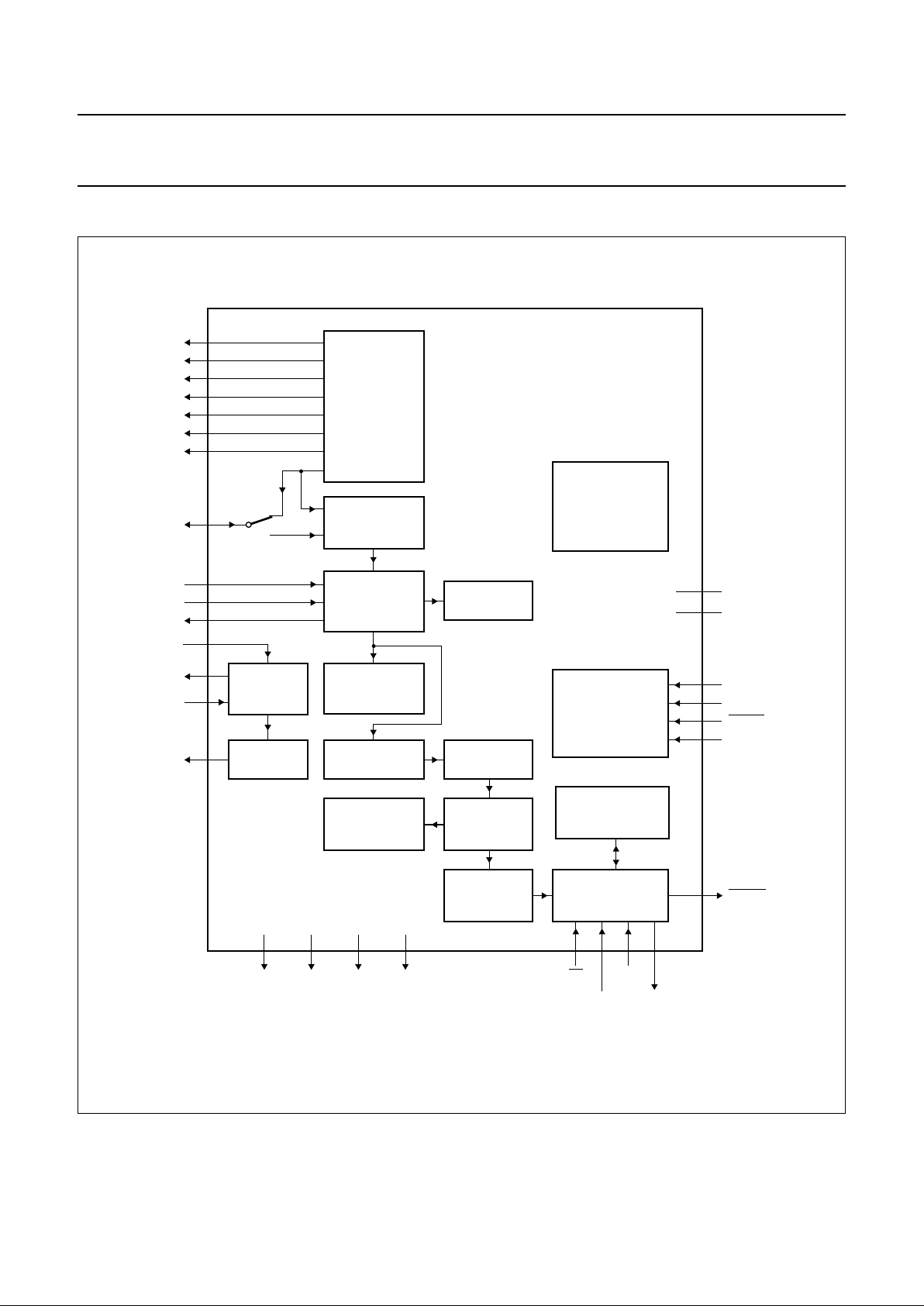
6 BLOCK DIAGRAM
Fig.1 Functional block diagram for PCD5013 pager decoder.
READY
MGR616
handbook, full pagewidth
22
S1
21
S2
20
S3
19
S4
18
S5
16
S6
15
S7
12
EXTS0
11
EXTS1
5
XTAL
2
OSCPD
6
EXTAL
32
CLKOUT
14
SYMCLK
23
S0
S0/IFIN
IFIN
27 28 30 31
26
RECEIVER
CONTROL
DEMODULATOR
&
DATA SLICER
SYNC
CORRELATOR
DE-
INTERLEAVER
76.8 kHz
OR 160 kHz
OSCILLATOR
CLOCK
GENERATOR
ADDRESS
COMPARATOR/
CORRELATOR
ERROR
CORRECTOR
NOISE
DETECTOR
SPI
BUFFER
SPI
INTERNAL
CONTROL
UNIT
EXTERNAL
CONTROL
UNIT
MISO
10
LOBAT
24
RESET
8
TEST3
4
TEST2
7, 29
V
SS1
, V
SS2
3, 13
V
DD1
, V
DD2
MOSI
SCK
SS
9
TOUT3
17
TOUT2
25
TOUT1
1
TOUT0
LOCAL
MESSAGE
FILTER
CONTROL/STATUS
REGISTERS
SYMBOL
SYNC
PCD5013
Page 5

1999 Apr 12 5
Philips Semiconductors Product specification
FLEX roaming decoder II PCD5013
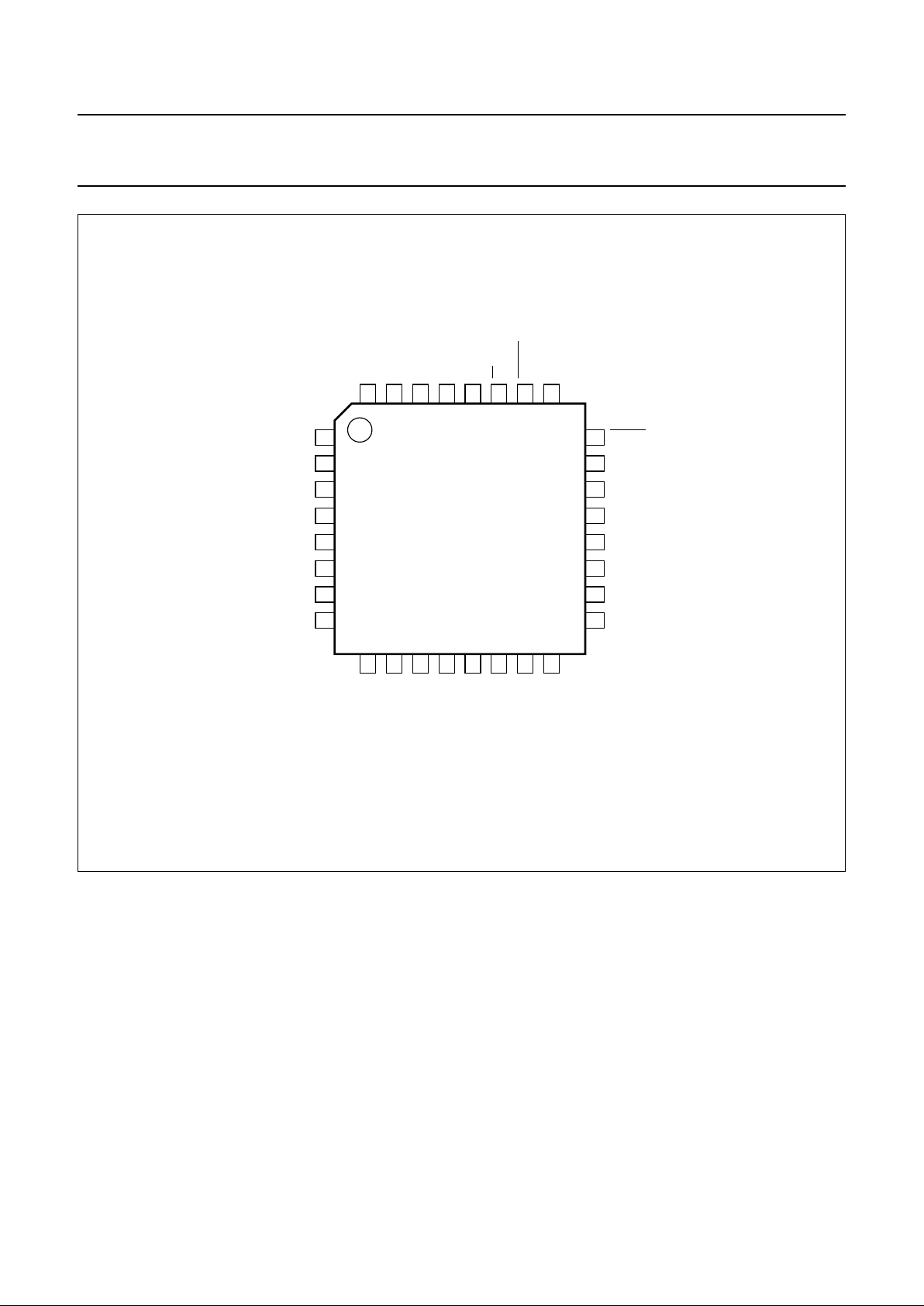
7 PINNING
Notes
1. These test outputs may be either left unconnected or connected to V
SS
in the application.
2. For a 160 kHz oscillator either a 38.4 or a 40 kHz output frequency can be selected. See Section 8.4.4.
SYMBOL PIN I/O DESCRIPTION
TOUT0 1 O 3-state test output; note 1
OSCPD 2 I internal oscillator power-down; connected to V
SS
when using the internal oscillator,
connected to VDD when using an external source
V
DD1
3 − supply voltage
TEST2 4 I manufacturing test mode input pin; has to be connected to V
SS
XTAL 5 O 76.8 or 160 kHz crystal oscillator output
EXTAL 6 I 76.8 or 160 kHz crystal oscillator input or external clock input
V
SS1
7 − ground supply
TEST3 8 I manufacturing test mode input pin; has to be connected to V
SS
TOUT3 9 O 3-state test output; note 1
LOBAT 10 I low battery voltage detect input
EXTS1 11 I most significant bit (MSB) of the symbol currently being decoded
EXTS0 12 I least significant bit (LSB) of the symbol currently being decoded
V
DD2
13 − supply voltage
SYMCLK 14 O recovered symbol clock output
S7 15 O receiver control output port, 3-state
S6 16 O receiver control output port, 3-state
TOUT2 17 O 3-state test output; note 1
S5 18 O receiver control output port, 3-state
S4 19 O receiver control output port, 3-state
S3 20 O receiver control output port, 3-state
S2 21 O receiver control output port, 3-state
S1 22 O receiver control output port, 3-state
S0/IFIN 23 I/O receiver control output port, 3-state when using external demodulator; limited
IF input 455 or 140 kHz when using internal demodulator
RESET 24 I active LOW reset input
TOUT1 25 O 3-state test output; note 1
READY 26 O output driven LOW when the PCD5013 is ready for an SPI packet
SS 27 I slave select input for SPI communications
SCK 28 I serial clock input for SPI communications
V
SS2
29 − ground supply
MOSI 30 I data input for SPI communications
MISO 31 O data output for SPI communications, 3-state
CLKOUT 32 O 38.4 kHz clock output (derived from 76.8 kHz oscillator); note 2
Page 6
1999 Apr 12 6
Philips Semiconductors Product specification
FLEX roaming decoder II PCD5013
Fig.2 Pin configuration.
handbook, full pagewidth
PCD5013
MGR619
1
2
3
4
5
6
7
8
24
23
22
21
20
19
18
17
9
10
11
12
13
14
15
16
32
31
30
29
28
27
26
25
TOUT0
OSCPD
V
DD1
TEST2
XTAL
EXTAL
V
SS1
TEST3
TOUT3
LOBAT
EXTS1
EXTS0
SYMCLK
S7
S6
V
DD2
TOUT2
S5
S3
S1
S2
S0/IFIN
S4
RESET
TOUT1
SCK
V
SS2
MOSI
MISO
CLKOUT
READY
SS
Page 7

1999 Apr 12 7
Philips Semiconductors Product specification
FLEX roaming decoder II PCD5013
8 FUNCTIONAL DESCRIPTION
8.1 General
The PCD5013 simplifies implementation of a FLEX
paging device by interfacing with off-the-shelf components
such as a paging receiver and a microcontroller or
microprocessor (called a host). The PCD5013 is fully
compatible with FLEXstack software which provides a
complete, platform independent, software driver for the
PCD5013.
The PCD5013 fully supports all aspects of the FLEX
protocol (version G1.9), and can operate in either
single-phase or any-phase mode. The PCD5013 supports
FLEX dynamic grouping, allowing up to 16 temporary
addresses to be enabled simultaneously. It is also capable
of retrieving real time information from a FLEX channel.
The PCD5013 connects to any receiver capable of
providing a 2-bit digital signal. The PCD5013 operates the
paging receiver in an efficient power consumption mode.
The PCD5013 has 8 receiver control lines used for
warming up, operating and shutting down a receiver in
stages.
The PCD5013 has the ability to detect a battery-low signal
from an external detector during the receiver control
sequences.
The PCD5013 carries out the following functions:
• Synchronises to a FLEX data stream
• Processes received, demodulated information
• Performs de-interleaving and error correction
• Selects calls addressed to the paging device using up to
16 programmable addresses
• Communicates the message information to the host.
The PCD5013 interfaces to a host through a serial
peripheral interface (SPI). The host can then interpret the
message information in an appropriate manner (numeric,
alphanumeric, binary, etc.). This function is provided by
the FLEXstack software.
When configured to use the internal demodulator, the
PCD5013 connects to a receiver capable of generating a
limited (i.e. 1-bit digitized) 455 or 140 kHz IF signal
(IF frequency automatically detected).
The PCD5013 enables the host to operate in a low-power
mode when monitoring a single channel for message
information. It has a 38.4 kHz clock output (40 kHz
available when using the internal demodulator) capable of
driving other devices, and has a 1-minute timer that offers
low-power support for a real-time clock function on the
host.The host can use receiver control lines which are not
required by the receiver as expansion ports to control other
peripheral devices.
8.2 Clocking, reset and start-up
8.2.1 O
SCILLATOR
The PCD5013 uses an inverting crystal oscillator.
The clock signal for the internal circuitry is derived via an
amplifier from the oscillator input pin EXTAL. Alternatively,
an external clock signal can be fed in at input pin EXTAL.
In this case the internal oscillator can be disabled by
pulling the OSCPD input pin HIGH. This reduces current
consumption and routes EXTAL directly to the internal
clock signal. When using a crystal, an external feedback
resistor and the load capacitances need to be connected
to pins EXTAL and XTAL (Fig.19). See Chapter 14 for the
recommended crystal parameters and the specification of
the oscillator transconductance to guarantee correct
start-up.
The PCD5013 oscillator can operate at either 76.8 kHz or
160 kHz by selecting the appropriate crystal. The choice of
frequency is determined by the setting of the IDE bit in the
configuration packet; see Section 8.4.4.
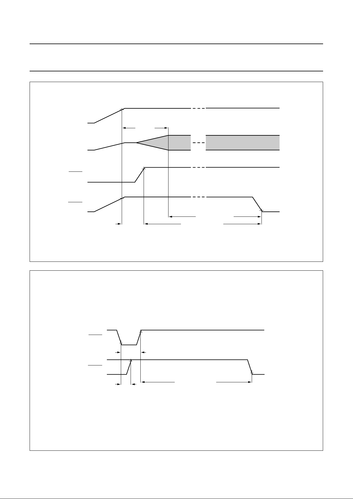
8.2.2 R
ESET AND START-UP CONDITIONS
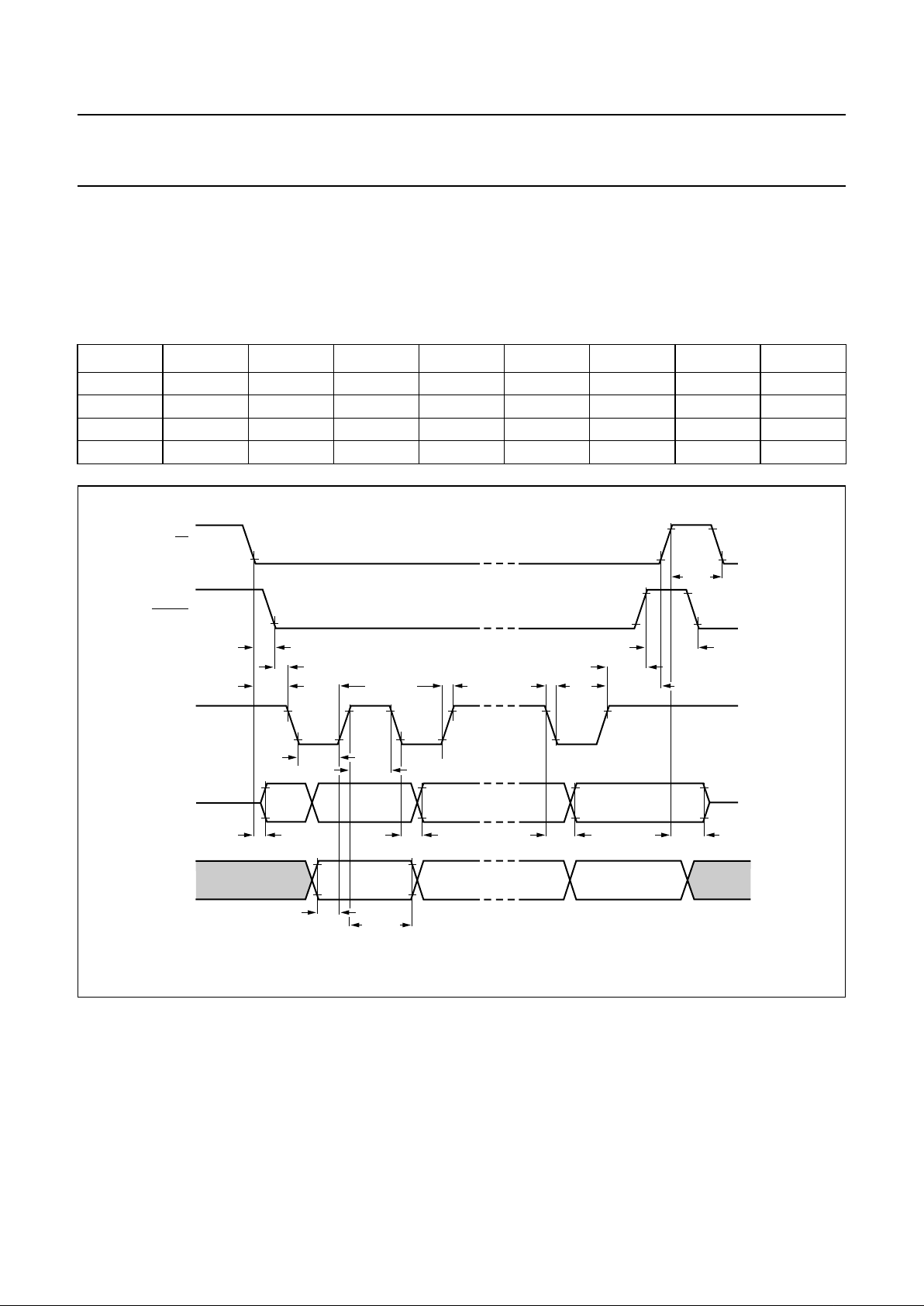
The PCD5013 is reset by pulling the RESET input LOW.
After releasing the RESET by pulling it HIGH, the
PCD5013 counts 76800 clock cycles (independent of the
oscillator frequency) before pulling READY LOW to
indicate that the decoder is ready for configuration via
the SPI.
See Fig.3 and Chapter 13 for the PCD5013 timing
specifications when power is applied.
See Fig.4 and Chapter 13 for the PCD5013 timing
specifications when it is reset.
After switch-on, the PCD5013 operates in Asynchronous
mode, periodically sampling the channel for incoming
data. As soon as data is detected, the PCD5013 maintains
the receiver on to synchronize to the channel. Once the
pager is synchronized to the channel it enters
Synchronous mode, switching the receiver on only for the
programmed frames.
When the receiver is programmed for Roaming operation,
the PCD5013 sends information which allows the host to
calculate when to switch frequencies in a roaming
network.
Page 8
1999 Apr 12 8
Philips Semiconductors Product specification
FLEX roaming decoder II PCD5013
Fig.3 Start-up timing.
handbook, full pagewidth
MBK031
t
h(rst)
t
WUL(osc-READY)
t
HL(RESET-READY)
t
strt(osc)
V
DD
oscillator
RESET
READY
Fig.4 Reset timing.
handbook, full pagewidth
MBK033
RESET
READY
t
LH(RESET-READY)
t
HL(RESET-READY)
t
W(rst)
Page 9

1999 Apr 12 9
Philips Semiconductors Product specification
FLEX roaming decoder II PCD5013
8.3 Serial Peripheral Interface (SPI)
8.3.1 G
ENERAL
All data communication between the PCD5013 and the
host is done via the SPI using 32-bit data packets at data
rates up to 1 Mbits/s. SPI transfers are full-duplex and can
be initiated by either the host which acts as the SPI master
providing the data clock for packet transfer, or the
PCD5013 as an SPI slave.
The host can send packets to configure or control the
PCD5013 or a checksum packet to validate SPI
communication (Section 8.4.2). The PCD5013 buffers
data packets, relating to received data, into a 32 packet
transmit buffer. The PCD5013 can send either a status
packet, a part ID packet, or packets from the transmit
buffer. In the event of a buffer overflow, the PCD5013
stops decoding and clears the transmit buffer.
8.3.2 SPI
INTERCONNECT
Connection on the PCD5013 consists of a READY pin and
4 SPI pins (SS, SCK, MOSI and MISO):
READY: output signal; indicates that data is available
from the PCD5013
SS: SPI select; used as PCD5013 chip select
SCK: serial clock; output from the host used for clocking
data
MOSI: master output slave input; data output from the
host
MISO: master input slave output; data output from the
PCD5013.
8.3.3 SPI
TRANSFER INITIATED BY THE HOST
The following steps occur when the host initiates an SPI
packet transfer, see Fig.5 for event timings:
1. The host selects the PCD5013 by driving the
SS pin LOW.
2. The PCD5013 indicates that it is ready to start the
SPI transfer by driving the
READY pin LOW.
3. The host clocks each of the 32 bits of the SPI packet
by pulsing SCK. Both the host and the PCD5013
sample data on the rising edge of SCK. Packets are
sent MSB first.
4. The PCD5013 pulls the READY line HIGH, to indicate
that the transfer is complete.
5. The host waits until the READY line is pulled HIGH,
then de-selects the PCD5013 SPI by driving the
SS pin HIGH.
6. The first 5 steps are repeated for each additional
packet.
8.3.4 SPI
TRANSFER INITIATED BY THE DECODER
The following steps occur when the PCD5013 initiates an
SPI packet transfer, see Fig.6 for event timings:
1. The PCD5013 initiates the SPI transfer by driving the
READY pin LOW.
2. If the PCD5013 is not already selected, the host
selects the PCD5013 SPI by driving the SS pin LOW.
3. The host clocks each of the 32 bits of the SPI packet
by pulsing SCK. Both the host and the PCD5013
sample data on the rising edge of SCK. Packets are
sent MSB first.
4. The PCD5013 pulls the READY line HIGH, to indicate
that the transfer is complete.
5. The host may then either de-select the SPI interface of
the PCD5013 (Fig.7) by driving the SS pin HIGH or
maintain SS LOW to continue sending packets to the
PCD5013.
Page 10

1999 Apr 12 10
Philips Semiconductors Product specification
FLEX roaming decoder II PCD5013
Fig.5 Typical multiple SPI transfers initiated by the host.
handbook, full pagewidth
MGK262
MISO
MOSI
SCK
Z
o(off)
(1) (5)
(4)
(2)
(3)
D31 D1 D0
D31 D1 D0
Z
o(off)
D31 D1 D0
D31 D1 D0
Z
o(off)
Z
o(off)
D31 D1 D0
D31 D1 D0
READY
SS
Numbers within parenthesis refer to sequence numbers, see Section 8.3.3.
Fig.6 Typical multiple SPI transfers initiated by the PCD5013.
handbook, full pagewidth
MGK263
MISO
MOSI
SCK
Z
o(off)
(2) (5)
(4)
(1)
(3)
D31 D1 D0
D31 D1 D0
Z
o(off)
Z
o(off)
Z
o(off)
D31 D1 D0
D31 D1 D0
D31 D1 D0
D31 D1 D0
READY
SS
Numbers within parenthesis refer to sequence numbers, see Section 8.3.4.
Page 11
1999 Apr 12 11
Philips Semiconductors Product specification
FLEX roaming decoder II PCD5013
Fig.7 Multiple SPI transfers initiated by the PCD5013 with SS maintained LOW.
handbook, full pagewidth
MGK264
MISO
MOSI
SCK
Z
o(off)
D31 D1 D0
D31 D1 D0
D31 D1 D0
D31 D1 D0
D31 D1 D0
D31 D1 D0
READY
SS
Page 12
1999 Apr 12 12
Philips Semiconductors Product specification
FLEX roaming decoder II PCD5013
8.3.5 SPI PACKET FORMAT
SPI data packets consist of an 8-bit ID (byte 3), followed
by 24 bits of information (byte 2 to byte 0). See Table 1,
note that bit 7 of byte 3 is the first bit on the bus.
8.3.6 SPI TIMING
See Fig.8 and Chapter 13 for the timing specifications of
the SPI.
Table 1 Packet bit assignments
BYTE BIT 7 BIT 6 BIT 5 BIT 4 BIT 3 BIT 2 BIT 1 BIT 0
3 D31 D30 D29 D28 D27 D26 D25 D24
2 D23 D22 D21 D20 D19 D18 D17 D16
1 D15 D14 D13 D12 D11 D10 D9 D8
0D7D6D5D4D3D2D1D0
Fig.8 SPI timing.
handbook, full pagewidth
MBK032
t
SCKL
t
SCKH
t
ACC(o)
Z
o(off)
t
DOV
t
h(i)(D)
t
su(i)(D)
T
cy(SCK)
t
LEAD1
SS
t
LEAD2
t
d(SS-READY)
t
READYH
t
r
t
f
t
LAG1
t
LAG2
t
SSH
READY
SCK
MISO D31 D0
D31 D0
MOSI
t
h(o)(D)
t
o(dis)
Page 13

1999 Apr 12 13
Philips Semiconductors Product specification
FLEX roaming decoder II PCD5013
8.3.7 HOST-TO-DECODER PACKETS OVERVIEW
This section summarises the packets which can be sent from the host to the decoder.
Table 2 Host-to-decoder packet ID map2
PACKET
ID (HEX) TYPE SECTION
00 checksum 8.4.6
01 configuration 8.4.4
02 control 8.4.7
03 all frame mode 8.8.4
04 operator message address enable 8.6.9
05 roaming control 8.4.9
06 timing control 8.4.10
07 to 0E reserved (host should never send) −
0F receiver line control 8.5.7
10 receiver control configuration (off setting) 8.5.4
11 receiver control configuration (warm-up 1 setting) 8.5.5.3
12 receiver control configuration (warm-up 2 setting) 8.5.5.3
13 receiver control configuration (warm-up 3 setting) 8.5.5.3
14 receiver control configuration (warm-up 4 setting) 8.5.5.3
15 receiver control configuration (warm-up 5 setting) 8.5.5.3
16 receiver control configuration (3200 sps sync setting) 8.5.6.2
17 receiver control configuration (1600 sps sync setting) 8.5.6.2
18 receiver control configuration (3200 sps data setting) 8.5.6.2
19 receiver control configuration (1600 sps data setting) 8.5.6.2
1A receiver control configuration (shut-down 1 setting) 8.5.8.1
1B receiver control configuration (shut-down 2 setting) 8.5.8.1
1C to 1F special (ignored by decoder) −
20 frame assignment (frames 112 to 127) 8.6.7
21 frame assignment (frames 96 to 111) 8.6.7
22 frame assignment (frames 80 to 95) 8.6.7
23 frame assignment (frames 64 to 79) 8.6.7
24 frame assignment (frames 48 to 63) 8.6.7
25 frame assignment (frames 32 to 47) 8.6.7
26 frame assignment (frames 16 to 31) 8.6.7
27 frame assignment (frames 0 to 15) 8.6.7
28 to 77 reserved (host should never send) −
78 user address enable 8.6.6
79 to 7F reserved (host should never send) −
80 user address assignment (user address 0) 8.6.6
81 user address assignment (user address 1) 8.6.6
82 user address assignment (user address 2) 8.6.6
Page 14

1999 Apr 12 14
Philips Semiconductors Product specification
FLEX roaming decoder II PCD5013
8.3.8 DECODER-TO-HOST PACKETS OVERVIEW
This section summarises the packets which can be sent from the PCD5013 to the host (Table 3).
Table 3 Decoder-to-host packet ID map
83 user address assignment (user address 3) 8.6.6
84 user address assignment (user address 4) 8.6.6
85 user address assignment (user address 5) 8.6.6
86 user address assignment (user address 6) 8.6.6
87 user address assignment (user address 7) 8.6.6
88 user address assignment (user address 8) 8.6.6
89 user address assignment (user address 9) 8.6.6
8A user address assignment (user address 10) 8.6.6
8B user address assignment (user address 11) 8.6.6
8C user address assignment (user address 12) 8.6.6
8D user address assignment (user address 13) 8.6.6
8E user address assignment (user address 14) 8.6.6
8F user address assignment (user address 15) 8.6.6
90 to FF reserved (host should never send) −
PACKET
ID (HEX) TYPE SECTION
00 block information word 8.7.9
01 address 8.7.2
02 to 57 vector or message (ID is word number in frame) 8.7.3 and 8.7.8
58 to 5F reserved −
60 roaming status 8.4.13
61 to 7D reserved −
7E receiver shutdown 8.4.12
7F status 8.4.11
80 to FE reserved −
FF part ID 8.4.5
PACKET
ID (HEX) TYPE SECTION
Page 15

1999 Apr 12 15
Philips Semiconductors Product specification
FLEX roaming decoder II PCD5013
8.4 Configuration and synchronisation
8.4.1 G
ENERAL
After a reset, all configuration data has to be (re)loaded
into the PCD5013 by the host using the SPI. PCD5013
features which do not change during operation are
configured using the configuration packet (Section 8.4.4),
the receiver control packets (Section 8.5) and the address
configuration packets (Section 8.6). PCD5013 features
which can be changed during operation are configured
using the control packet. The checksum packet ensures
proper communication between the host and the
PCD5013.
8.4.2 SPI
SECURITY ALGORITHM
The PCD5013 provides a security algorithm to verify
correct SPI operation (Figs 9 and 10). The PCD5013
maintains a checksum register equal to the result of
XORing the 24 data bits of every packet it receives, except
the checksum packet 00H and special packets
1CH to 1FH. When the PCD5013 is reset, the internal
checksum register is initialized to the 24-bit part ID defined
in the part ID packet.
Immediately following a reset and whenever the host
sends a packet other than a checksum packet, the
SPI output of status and data (SPI transmit) is disabled.
The PCD5013 then initiates SPI transfers continuously,
sending the part ID packet (Section 8.4.5). Note that when
SPI transmit is disabled all decoding and timing functions
are unaffected. The SPI transmit can be enabled by
sending a checksum packet for which the checksum value
matches the checksum register.
Checksum packets sent when the SPI transmit is enabled,
are ignored by the PCD5013 irrespective of the value of
the checksum packet data bits. Thus when the PCD5013
initiates an SPI transfer and the host has no data to send,
the host should send the checksum packet so as not to
disable the SPI transmit. The data in the checksum packet
could be a null packet (32-bit stream of all zeros).
Sending a packet other than the checksum packet when
the SPI transmit is enabled causes the SPI transmit to be
disabled until a checksum packet is sent with the correct
value. Thus when the host re-configures the PCD5013
after a reset, the SPI transmit is disabled until the host
sends a checksum packet at the end of the configuration
data, with the checksum value equal to the result of
XORing together the data bits of each of the configuring
packets and the data bits of the part ID packet.
If the SPI transmit is enabled and a receiver shutdown
packet is pending, the receiver shutdown packet is sent. If
there is no receiver shutdown packet pending, but there is
a roaming status packet pending, the roaming status
packet is sent. If neither the receiver shutdown packet nor
the roaming status packet is pending and there is data in
the transmit buffer, the PCD5013 initiates an SPI transfer
sending a packet from its transmit buffer. The PCD5013
sends the status packet (which is not buffered) when the
host initiates an SPI transfer and the transmit buffer is
empty.
Fig.9 SPI transmit functional block diagram.
handbook, full pagewidth
MGR618
ROAMING STATUS REGISTER
STATUS REGISTER
SPI
SECURITY
ALGORITHM
MUX
SPI TRANSMIT REGISTER
MISO
32 × 32 DATA PACKET
FIFO TRANSMIT
BUFFER
32
RECEIVER SHUTDOWN REGISTER
32
PART ID REGISTER
32
32
32
32
Page 16

1999 Apr 12 16
Philips Semiconductors Product specification
FLEX roaming decoder II PCD5013
Fig.10 SPI security algorithm.
handbook, full pagewidth
MGR617
reset
PCD5013 disables
SPI transmit
PCD5013 disables
SPI transmit
PCD5013 sets
checksum registers to
the XOR of the packet
data bits with the
checksum register bits
PCD5013 enables
SPI transmit
Y
Y
YN
N
N
PCD5013 initializes
checksum register
to part ID value
PCD5013 initiates
part ID packet
PCD5013 waits for
SPI packet from host
checksum packet?
PCD5013
SPI transmit
enabled?
packet data
matches checksum
register data?
Page 17
1999 Apr 12 17
Philips Semiconductors Product specification
FLEX roaming decoder II PCD5013
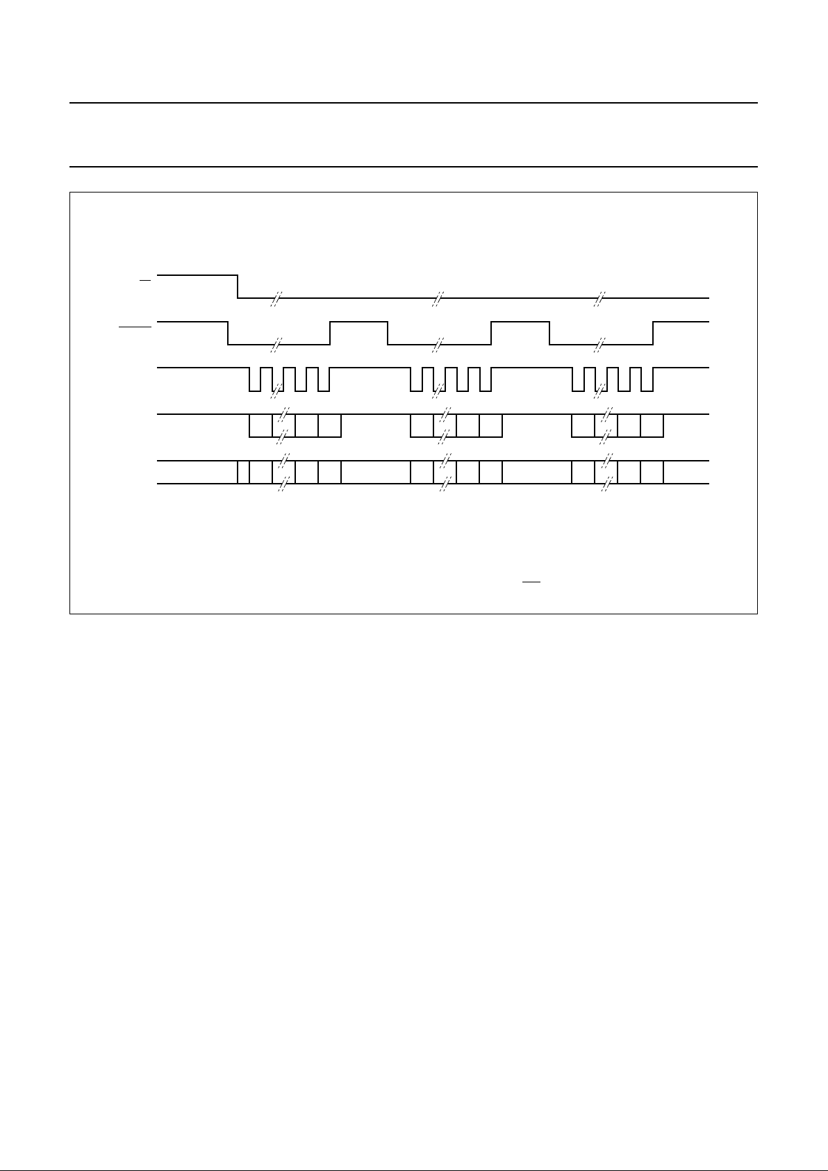
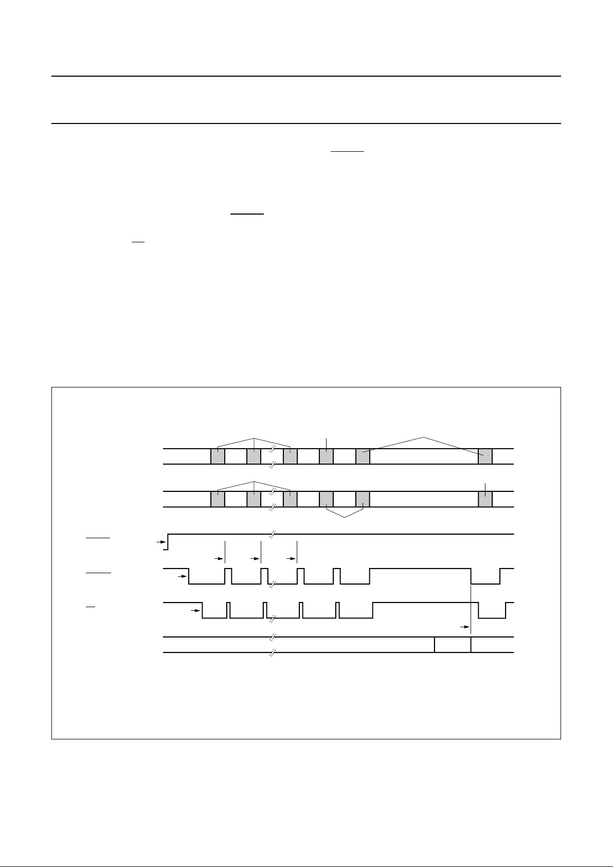
8.4.3 CONFIGURATION SEQUENCE
A typical configuration and synchronisation sequence
would be as follows, see Fig.11 for event timings:
1. The PCD5013 is reset by the host.
2. After 76800 clock cycles the PCD5013 interrupts the
host to read the part ID by pulling the READY
line LOW.
3. The host pulls SS LOW at the start of each
SPI transfer and clocks out the part ID data.
4. The host configures the following aspects of PCD5013
operation:
a) General configuration (Section 8.4.4)
b) Receiver operation (Section 8.5)
c) FLEX CAPCODE configuration (Section 8.6).
The PCD5013 writes a part ID packet in response to
each incoming packet.
5. At the end of each packet the PCD5013 pulls the
READY line HIGH, and then LOW again to indicate
that packet processing is complete.
6. The host writes a control packet to enable FLEX
decoding in the PCD5013 (Section 8.4.7).
7. The host writes a checksum packet to enable SPI data
output by the PCD5013 (Section 8.4.2).
8. On recognising a SYNC word, the PCD5013
synchronises to the channel.
9. The PCD5013 initiates an SPI transfer writing the
status packet, indicating that it is now in synchronous
mode.
Fig.11 Typical configuration and synchronization sequence.
handbook, full pagewidth
MBK097
SPI
DECODER-TO-HOST
RESET
READY
SS
FLEX DATASTREAM
SPI
HOST-TO-DECODER
checksum packet
(7)
control packet
(6)
partid packet
(4)
configuration packets
(addresses, receiver etc.)
status packet
(9)
partid packet
(4)
(1)
(2)
(3)
(5) (5) (5)
(8)
SYNC
Numbers within parenthesis refer to sequence numbers, see Section 8.4.3.
Page 18

1999 Apr 12 18
Philips Semiconductors Product specification
FLEX roaming decoder II PCD5013
8.4.4 CONFIGURATION PACKET (ID = 01H)
The configuration packet defines a number of different
configuration options for the PCD5013. The PCD5013
ignores this packet when decoding is enabled,
i.e. the ON bit in the control packet is set (Table 12).
DFC: disable fractional clock (Table 8). When this bit is set
and IDE is set, the CLKOUT signal generates a 40 kHz
signal (EXTAL divided-by-4). When this bit is cleared and
IDE is set, the CLKOUT signal generates a 38.4 kHz signal
(EXTAL fractionally divided by25⁄6). This bit has no effect
when IDE is cleared. Value after reset = 0.
IDE: internal demodulator enable (Table 8). When this bit
is set, the internal demodulator is enabled and the clock
frequency at EXTAL is expected to be 160 kHz. When this
bit is cleared, the internal demodulator is disabled and the
clock frequency at EXTAL is expected to be 76.8 kHz.
Value after reset = 0.
OFD: oscillator frequency difference (Tables 4 and 8).
These bits represent the maximum frequency difference
between the 76.8 kHz oscillator (accounting for ageing,
temperature variation, manufacturing tolerance etc.) and
the worst case transmitter bit rate (specified as ±25 parts
per million (ppm) in the FLEX specification).
For example, if the transmitter tolerance is ±25 ppm and
the 76.8 kHz oscillator tolerance is ±140 ppm, the
transmitter-oscillator frequency difference is ±165 ppm
and OFD should be cleared (300 ppm maximum). Value
after reset = 0. Note that configuring a smaller frequency
difference in this packet results in lower power
consumption due to higher receiver battery save ratios.
Table 4 Oscillator frequency difference
PCE: partial correlation enable (Table 8). When this bit is
set, partial correlation of addresses is enabled. When
partial correlation is enabled, the PCD5013 shuts down
the receiver before the end of the last FLEX block which
contains addresses if it can determine that none of the
addresses in that FLEX block matches any enabled
address in the PCD5013. When this bit is cleared, the
receiver is controlled as in the PCD5008. Value after
reset = 0.
OFD
1
OFD
0
FREQUENCY DIFFERENCE
(ppm)
00±300
01±150
10±75
11±0
SP: signal polarity (Tables 8, 5 and 6). These bits set the
polarity of EXTS1 and EXTS0 input signals. The polarity of
the EXTS1 and EXTS0 bits is determined by the receiver
design. Value after reset = 0.
Table 5 Input signal polarity
Table 6 FLEX 4 level FSK modulation (SP = 00)
SME: synchronous mode enable (Table 8). When this bit
is set, a status packet is sent automatically whenever the
synchronous mode update (SMU) bit in the status packet
is set. This happens whenever a change occurs in the
synchronous mode (SM) status bit, which indicates that
the decoder is synchronized to a FLEX data stream.
The host can use the SM bit in the status packet as an
in-range/out-of-range indication. Value after reset = 0.
COD: clock output disable (Table 8). When this bit is
cleared, a 38.4 or 40 kHz signal is output on the
CLKOUT pin (depending on the values of IDE and DFC).
When this bit is set, the CLKOUT pin is driven LOW. Value
after reset = 0.
• Setting and clearing this bit can cause pulses on the
CLKOUT pin that are less than one half the 38.4 kHz
period.
• When the clock output is enabled and not set for
intermittent operation (see ICO in this packet), the
CLKOUT pin always outputs the clock signal even when
the PCD5013 is in reset (as long as a clock signal is
available to the PCD5013 oscillator).
• When the PCD5013 is used in internal demodulator
mode (i.e. uses a 160 kHz oscillator), the CLKOUT pin
is 80 kHz from reset until the time the IDE bit is set.
SP
1
SP
0
SIGNAL POLARITY
EXTS1 EXTS0
0 0 normal normal
0 1 normal inverted
1 0 inverted normal
1 1 inverted inverted
EXTS1 EXTS0
DEVIATION
(Hz)
1 0 +4800
1 1 +1600
01 −1600
00 −4800
Page 19

1999 Apr 12 19
Philips Semiconductors Product specification
FLEX roaming decoder II PCD5013
LBP: low battery polarity (Table 8). This bit defines the
polarity of the PCD5013’s LOBAT pin: When this bit is set,
a HIGH at input LOBAT represents a low battery condition.
The LB bit in the status packet is initialized to the inverse
(i.e. inactive) value of the LBP bit when the PCD5013 is
turned on (by setting the ON bit in the control packet).
When the PCD5013 is turned on, the first low battery
update in the status packet is sent to the host when a low
battery condition is detected on the LOBAT pin. Value
after reset = 0.
MOT: maximum off time (Table 8). When this bit is set, the
PCD5013 assumes that the service provider leaves up to
1 minute between transmitted frames. When this bit is
clear, the PCD5013 assumes that there can be up to
4 minutes between transmitted frames. This bit has no
effect if AST in the Timing Control Packet is non-zero.
Value after reset = 0.
MTE: minute timer enable (Table 8). When this bit is set,
a status packet is sent at one minute intervals with the
minute time-out (MT) bit in the status packet set. When
this bit is clear, the internal 1-minute timer stops counting.
See Section 8.4.8 for details of 1-minute timer operation.
Note that the minute timer is not accurate using a 160 kHz
oscillator until the IDE bit is set. Value after reset = 0.
ICO: intermittent clock out (Table 8). When this bit is clear
and COD is clear, a 38.4 or 40 kHz (depending on the
values of IDE and DFC) signal is output on the CLKOUT
pin. When this bit is set and COD is clear, the clock is only
output on the CLKOUT pin while the receiver is not in the
Off state. The clock is output for a few cycles before the
receiver transitions from the off state and for a few cycles
after the receiver transitions to the off state (this is to insure
that the receiver receives enough clocks to detect and
process the changes to and from the off state).
The CLKOUT pin is driven LOW when it is not driving a
clock.
Note that when the clock is automatically enabled and
disabled (i.e. when ICO is set), the CLKOUT signal
transitions are clean (i.e. no pulses less than half the clock
period) when it transitions between no clock and clocked
output. This bit has no effect when COD is set. Value after
reset = 0.
8.4.5 P
ART ID P ACKET (ID = FFH)
The part ID packet is output by the PCD5013 SPI
whenever the SPI transmit is disabled due to the
checksum feature. The value of the part ID packet for the
PCD5013 is FF000308H.
MDL: model (Table 9). The PCD5013 model value is 0.
CID: compatibility ID (Table 9). This value describes other
parts with the same model number, which are compatible
with this part.
Table 7 CID Compatibilities
REV: revision (Table 9). This identifies the manufacturing
version of the PCD5013. For the PCD5013 the value is 8.
8.4.6 C
HECKSUM PACKET (ID = 00H)
See Table 10 for checksum packet bit assignment.
CV: checksum value (24 bits), see Section 8.4.2.
BIT COMPATIBILITY
VALUE FOR
PCD5013
CID
0
Alphanumeric Decoder I 1 (true)
CID
1
Roaming Decoder I 1 (true)
CID
2
Numeric Decoder 0 (false)
Table 8 Configuration packet bit assignments
BYTE BIT 7 BIT 6 BIT 5 BIT 4 BIT 3 BIT 2 BIT 1 BIT 0
300000001
2 0 DFC 0 0 0 IDE OFD
1
OFD
0
100000PCESP
1SP0
0 SME MOT COD MTE LBP ICO 0 0
Page 20

1999 Apr 12 20
Philips Semiconductors Product specification
FLEX roaming decoder II PCD5013
Table 9 Part ID packet bit assignments
Table 10 Checksum packet bit assignments
BYTE BIT 7 BIT 6 BIT 5 BIT 4 BIT 3 BIT 2 BIT 1 BIT 0
311111111
2 MDL
1
MDL
0
CID
13
CID
12
CID
11
CID
10
CID
9
CID
8
1 CID
7
CID
6
CID
5
CID
4
CID
3
CID
2
CID
1
CID
0
0 REV
7
REV
6
REV
5
REV
4
REV
3
REV
2
REV
1
REV
0
BYTE BIT 7 BIT 6 BIT 5 BIT 4 BIT 3 BIT 2 BIT 1 BIT 0
300000000
2CV23CV
22
CV
21
CV
20
CV
19
CV
18
CV
17
CV
16
1CV15CV
14
CV
13
CV
12
CV
11
CV
10
CV
9
CV
8
0CV
7CV6
CV
5
CV
4
CV
3
CV
2
CV
1
CV
0
Page 21

1999 Apr 12 21
Philips Semiconductors Product specification
FLEX roaming decoder II PCD5013
8.4.7 CONTROL PACKET (ID = 02H)
The control packet defines a number of different control
bits for the PCD5013.
FF: force frame 0 to 7 (Table 12). When set, each of these
bits forces the PCD5013 to decode one of the FLEX
frames 0 to 7 irrespective of the system collapse value (for
details of collapse values see Section 8.6.2). For example,
if the system collapse causes the PCD5013 to decode
frames 0, 32, 64 and 96, setting FF2 causes the PCD5013
to also decode FLEX frame 2. This may be used to
acquire transmitted time information or channel attributes
(e.g. Local ID). Value after reset = 0.
SPM: single phase mode (Table 12). When this bit is set,
the PCD5013 decodes only one of the transmitted phases.
When this bit is clear, the PCD5013 decodes all
transmitted phases. This value is determined by the
CAPCODE (Section 8.6). A change to this bit while the
PCD5013 is on does not take effect until the next block 0
of a frame. Value after reset = 0.
PS: phase select (Tables 11 and 12). When the SPM bit is
set, these bits define which phase the PCD5013 shall
decode. This value is determined by the CAPCODE
(Section 8.6). A change to these bits, while the PCD5013
is on, does not take effect until the next block 0 of a frame.
Value after reset = 0.
Table 11 Phase selection (by PS bits)
PS
1
PS
0
DECODED PHASE (BASED ON
FLEX DATA RATE)
1600 bits/s 3200 bits/s 6400 bits/s
00AAA
01AAB
10 A C C
11 A C D
SBI: send block information words (BIW) 2 to 4
(Table 12). When this bit is set, BIWs with time and date
information and BIWs received in error are sent to the host,
(Section 8.7.9). Value after reset = 0.
MTC: minute timer clear (Table 12). Setting this bit causes
the 1-minute timer to restart from 0 (Section 8.4.8).
ON: turn on decoder (Table 12). When this bit is set, the
PCD5013 decodes FLEX signals. If this bit is cleared,
signal processing stops. However, to assure proper
operation, the PCD5013 requires that it be set into
asynchronous mode when turned off. To achieve that the
following sequence must be used:
1. Send control packet with ON bit clear (decoder off)
2. Send control packet with ON bit set (decoder on)
3. Send control packet with ON bit clear (decoder off).
Timing between these steps is specified below and is
measured from the positive edge of the last clock of one
packet to the positive edge of the last clock of the next
packet.
• The minimum time between steps 1 and 2 is the greater
of 2 ms or the programmed shut-down time.
The programmed shut-down time is the sum of all of the
times programmed in the used receiver shut-down
settings packets.
• There is no maximum time between steps 1 and 2.
• The minimum time between steps 2 and 3 is 2 ms.
• The maximum time between steps 2 and 3 is the
programmed warm-up time minus 2 ms.
The programmed warm-up time is the sum of all the
times programmed in the used receiver warm-up
settings packets.
EAE: end of addresses enable. When this bit is set, the EA
bit in the Status Packet is PCD5013 set immediately after
the PCD5013 decodes the last address word in the frame
if any of the enabled PCD5013 addresses was detected in
the frame. When this bit is cleared, the EA bit is never set.
Table 12 Control packet bit assignments
BYTE BIT 7 BIT 6 BIT 5 BIT 4 BIT 3 BIT 2 BIT 1 BIT 0
300000010
2FF
7FF6
FF
5
FF
4
FF
3
FF
2
FF
1
FF
0
1 0 SPM PS
1
PS
0
0000
0 0 SBI 0 MTC 0 0 EAE ON
Page 22

1999 Apr 12 22
Philips Semiconductors Product specification
FLEX roaming decoder II PCD5013
8.4.8 OPERATING THE 1-MINUTE TIMER
The PCD5013 provides a 1-minute timer which allows the
host to implement a time-of-day function while maintaining
low-power operation. The 1-minute timer is enabled using
the MTE bit in the configuration packet (Section 8.4.4).
When the 1-minute timer is enabled, a status packet is
sent at 1-minute intervals with the MT bit set
(Section 8.4.11). When the MTE bit is clear, the internal
1-minute timer stops counting. When the host sends a
control packet with MTC bit set, the 1-minute timer restarts
from 0. This allows accurate setting of a time-of-day
function.
8.4.9 R
OAMING CONTROL PACKET (ID = 05H)
The roaming control packet controls the features of the
PCD5013 that allow implementation of a roaming pager.
IRS: ignore re-synchronization signal (Table 13). When
this bit is set, the PCD5013 does not go asynchronous
when detecting an Ar or Ar signal during searches for
A-words. It merely reports that the re-synchronization
signal was received by setting RSR to 1 in the Roaming
Status packet. This allows the host to decide what to do
when the paging device is synchronous to more than one
channel and only one channel is sending the
re-synchronization signal. It also prevents the PCD5013
from losing synchronization when it detects the
re-synchronization signal while the paging device is
checking an unknown channel. This bit is set and cleared
by the host. Value after reset = 0.
NBC: network bit check (Table 13). Setting this bit enables
reporting of the received network bit value (NBU and n) in
the Roaming Status Packet. Setting this bit also makes the
PCD5013 abandon a frame after the Frame Info word
without synchronizing to the frame if the frame information
word is uncorrectable or if the n bit in the frame information
word is not set. If the PCD5013 is in synchronous mode
when this occurs (probably due to synchronizing to a
second channel), it maintains synchronization to the
original channel.
If the PCD5013 is in asynchronous mode when this
occurs, it stays in asynchronous mode and end the A-word
search. This is done to avoid synchronizing to a
non-roaming channel when searching for roaming
channels. This bit is set and cleared by the host. Value
after reset = 0.
MCM: manual collapse mode (Table 13). When this bit is
set, the PCD5013 behaves as if the system collapse
was 7. The PCD5013 does not apply the received system
collapse to the AF bits. When this bit is set, the received
system collapse is reported to the host via SCU and RSC
in the Roaming Status Packet. This is so the host can
modify the AF bits based on the system collapse of the
channel. This bit is set and cleared by the host. Value after
reset = 0.
IS1: invert EXTS1 (Table 13). Setting this bit inverts the
expected polarity of the EXTS1 pin from the way it is
configured by SP 1 in the Configuration Packet (e.g. if both
IS1 and SP 1 are set, the polarity of the EXTS1 pin is
untouched). This bit is intended to be changed when a
change in a channel changes the polarity of the received
signal. This bit is set and cleared by the host. This bit has
the equivalent effect when using the internal demodulator.
Value after reset = 0.
SDF: stop decoding frame (Table 13). Setting this bit
causes the PCD5013 to stop decoding a frame without
losing frame synchronization. This bit is set by the host,
and cleared by the PCD5013 once it has been processed.
The packet with the SDF bit set must be sent after
receiving the status packet with EA bit set. It must be sent
within 40 ms of the end of block in which the PCD5013 set
the EA bit. Value after reset = 0.
RSP: receiver shutdown packet enable (Table 13). When
this bit is set, a Receiver Shutdown Packet is sent
whenever the receiver is shut down. The receiver
shutdown packet informs the host that the receiver
shutdown, and gives the time period before the PCD5013
automatically warms the receiver back up. Value after
reset = 0.
Table 13 Roaming Control Packet bit assignments
BYTE BIT 7 BIT 6 BIT 5 BIT 4 BIT 3 BIT 2 BIT 1 BIT 0
300000101
2 IRS NBC MCM IS1 SDF RSP SND CND
1 RND ABI SAS DAS AF
11
AF
10
AF
9
AF
8
000MFC
1
MFC
0
0 0 MCO
1
MCO
0
Page 23

1999 Apr 12 23
Philips Semiconductors Product specification
FLEX roaming decoder II PCD5013
SND: start noise detect (Table 13). Setting this bit while
the PCD5013 is battery saving causes it to warm-up the
receiver, run a noise detect, and report the result of the
noise detect via NDR in the Roaming Status Packet.
This bit is set by the host, and cleared by the PCD5013
once it has been processed. If the time comes for the
PCD5013 to warm-up automatically or the SAS bit is set
while an SND is being processed, the noise detect is
abandoned and the abandoned noise detect result
(NDR = 01) is sent in the Roaming Status Packet. Value
after reset = 0.
CND: continuous noise detect (Table 13). Setting this bit
causes the PCD5013 to do continuous noise detects
during the decoded block data of a frame. The results of
the noise detect is only reported if noise is detected
(NDR = 11). Only one noise detected result (NDR = 11) is
sent per block. If the PCD5013 has not completed a noise
detect when it shuts down for the frame, that noise detect
is abandoned, but no abandon result (NDR = 01) is sent.
This bit is set and cleared by the host. Value after
reset = 0.
RND: report noise detects (Table 13). Setting this bit
causes the PCD5013 to report the results of the noise
detects it does under normal asynchronous operation
(when first turned on and when asynchronous).
The results of the noise detect is reported via NDR in the
Roaming Status Packet. This bit is set and cleared by the
host. Value after reset = 0.
ABI: all block information words (Table 13). When this bit
is set, the PCD5013 sends all received Block Information
words 2-4 to the host. Note: Setting the SBI bit in the
Control Packet only enables errored and real-time clock
related block info words. Value after reset = 0.
SAS: start A-word search (Table 13). Setting this bit while
in asynchronous battery save mode causes the PCD5013
to warm-up the receiver and run an A-word search.
If, during the A-word search, the PCD5013 finds sufficient
FLEX signal, it enters synchronous mode and start
decoding the frame. If the A-word search times-out without
finding sufficient FLEX signal, it enters a battery save
mode and continue doing periodic noise detects.
The time-out for the A-word searches is controlled by the
AST bits in the Timing Control Packet and the MOT bit in
the Configuration Packet. The A-word search takes priority
over noise detects. Therefore, if the PCD5013 is
performing an A-word search and the time comes to do
automatic noise detect, the noise detect is not performed.
This bit is set by the host, and cleared by the PCD5013
once it has been acted on. Value after reset = 0.
MFC: missed frame control (Tables 14 and 13). These bits
control the frames for which missing frame data (MS1,
MFI, MS2, MBI, and MAW) is reported in the Roaming
Status Packet. Value after reset = 0.
Table 14 Missed Frame Control (MFC bits)
MCO: maximum carry on (Table 13). The value of these
bits sets the maximum carry on that the PCD5013 follows.
For example, if the PCD5013 receives a carry on of 3 over
the air and MCO is set to 1, the PCD5013 only carries on
for one frame. Value after reset = 3.
DAS: disable A-word search (Table 13). When this bit is
set, an A-word search does not automatically occur after a
noise detect in asynchronous mode finds FLEX signal.
This includes automatic noise detects and noise detects
initiated by the host by setting SND. The PCD5013 shuts
down the receiver after the noise detect completes
regardless of the result. When this bit is cleared, A-word
searches occur after a noise detect finds signal in
asynchronous mode. Value after reset = 0.
MFC
1
MFC0MISSING FRAME DATA REPORTED
0 0 never
0 1 only during frames 0 through 3
1 0 only during frames 0 through 7
1 1 always
Page 24

1999 Apr 12 24
Philips Semiconductors Product specification
FLEX roaming decoder II PCD5013
8.4.10 TIMING CONTROL PACKET (ID = 06H)
The timing control packet gives the host control of the
timing used when the PCD5013 is in asynchronous mode.
The packet ID for the timing control packet is 6.
AST: A-word search time (Table 15). The value of these
bits sets the A-word search time for all asynchronous
A-word searches in units of 80 ms (e.g. value of 1 is 80 ms,
a value of 2 is 160 ms, etc.). If the value is 0, the PCD5013
defaults to the 1-minute (MOT = 1) or 4-minute (MOT = 0)
A-word search time controlled by the MOT bit in the
configuration packet. Value after reset = 0.
ABT: asynchronous battery-save time (Table 15).
The value of these bits sets the battery save time (time
from the beginning of one automatic noise detect to the
beginning of the next automatic noise detect) in
asynchronous mode in units of 80 ms (e.g. value of 1 is
80 ms, a value of 2 is 160 ms, etc.) If the value is 0, the
battery save time is set to the default value of 1.5 seconds.
The minimum allowed ABT is 320 ms, therefore values of
1, 2, 3, and 4 are invalid. Value after reset = 0.
8.4.11 S
TATUS PACKET (ID = 7FH)
The status packet contains various types of information
that the host may require and is sent to the host:
• Whenever the PCD5013 is polled and has no other data
to send
• On events for which the PCD5013 is configured to send
the status packet (Sections 8.4.4 and 8.4.7). In this
case, the PCD5013 prompts the host to read a status
packet for the following conditions:
– SMU bit in the status packet and the SME bit in the
configuration packet are set
– MT bit in the status packet and the MTE bit in the
configuration packet are set
– EOF bit in the status packet is set
– LBU bit in the status packet is set
– EA bit in the status packet is set
– BOE bit in the status packet is set.
FIV: frame information valid (Table 16). This bit is set,
when a valid frame information word has been received
since becoming synchronous to the system and the
f and c fields contain valid values. If this bit is clear, no
valid frame information words have been received since
the PCD5013 became synchronous to the system.
This value changes from 0 to 1 at the end of block 0
(Fig.18) of the frame in which the first frame information
word was properly received. It is cleared when the
PCD5013 goes into asynchronous mode (see SM bit
below). This bit is initialized to 0 when the PCD5013 is
reset and when the PCD5013 is turned off by clearing the
ON bit in the control packet.
f: current frame number (Table 16). This value is updated
every frame regardless of whether the PCD5013 needs to
decode the frame. This value changes to its proper value
for a frame at the end of block 0 of the frame. The value of
these bits is not guaranteed when FIV is 0.
c: current system cycle number (Table 16). This value is
updated every frame regardless of whether the PCD5013
needs to decode the frame. This value changes to its
proper value for a frame at the end of block 0 of the frame.
The value of these bits is not guaranteed when FIV is 0.
SM: synchronous mode (Table 16). This bit is set, when
the PCD5013 is synchronous to the system.
The PCD5013 sets this bit when the first synchronization
words are received. It clears this bit when the PCD5013
has not properly received both synchronization words in
any frame for 8, 16, or 32 minutes (depending on the
number of assigned frames and the system collapse). This
bit is initialized to 0 when the PCD5013 is reset and when
it is turned off by clearing the ON bit in the control packet.
Table 15 Timing Control Packet bit assignments
BYTE BIT 7 BIT 6 BIT 5 BIT 4 BIT 3 BIT 2 BIT 1 BIT 0
300100f
2
f
1
f
0
200000000
1 AST
7
AST
6
AST
5
AST
4
AST
3
AST
2
AST
1
AST
0
0 ABT
7
ABT
6
ABT
5
ABT
4
ABT
3
ABT
2
ABT
1
ABT
0
Page 25

1999 Apr 12 25
Philips Semiconductors Product specification
FLEX roaming decoder II PCD5013
SMU: synchronous mode update (Table 16). This bit is set
if the SM bit has been updated in this packet. After the
PCD5013 has been turned on, this bit is set when the first
synchronization words are found (SM changes to 1) or
when the first synchronization search period (meaning the
receiver is active during this time) expires (SM stays 0),
after the PCD5013 is turned on. The latter condition gives
the host the option of assuming the paging device is in
range when it is turned on, and displaying out-of-range
only after the initial search period expires. After the initial
synchronous mode update, the SMU bit is set whenever
the PCD5013 switches from/to synchronous mode. The bit
is cleared when read. Changes in the SM bit due to turning
off the PCD5013 does not set the SMU bit. This bit is
initialized to 0 when the PCD5013 is reset.
LB: low battery (Table 16). Set to the value last read from
the LOBAT pin. The host controls when the LOBAT pin is
read via the receiver control packets. This bit is initialized
to 0 at reset. It is also initialized to the inverse of the
LBP bit in the configuration packet, when the PCD5013 is
turned on, by setting the ON bit in the control packet.
LBU: low battery update (Table 16). This bit is set if the
value on two consecutive reads of the LOBAT pin yielded
different results. The bit is cleared when read. The host
controls when the LOBAT pin is read via the receiver
control packets. Changes in the LB bit due to turning on
the PCD5013 do not cause the LBU bit to be set. This bit
is initialized to 0 when the PCD5013 is reset.
EOF: end of frame (Table 16). Set when the PCD5013 is
in all frame mode (AFM) (Section 8.8.4), and the end of
the frame has been reached. The PCD5013 is in the AFM
if the AFM enable counter is non-zero, if any temporary
address enabled (TAE) counter is non-zero (Section 8.8.4)
or if the FAF bit in the AFM packet is set. The bit is cleared
when read and initialized to 0 when the PCD5013 is reset.
MT: minute time-out (Table 16). Set if one minute has
elapsed. The bit is cleared when read. This bit is initialized
to 0 when the PCD5013 is reset.
BOE: buffer overflow error (Table 16). Set when
information has been lost owing to slow host response
time. When the PCD5013 detects that its SPI transmit
buffer has overflowed, it clears the transmit buffer, turns off
decoding by clearing the ON bit in the control packet, and
sets this bit. The bit is cleared when read. This bit is
initialized to 0 when the PCD5013 is reset.
EA: end of addresses (Table 16). If EAE of the control
packet is set and an address is detected in a frame, EA is
set after the PCD5013 processes the last address in the
frame. Since data packets take priority over the status
packet, the status packet with the EA bit set is guaranteed
to come after all address packets for the frame. Cleared
when read. This bit is initialized to 0 when the PCD5013 is
reset.
x: unused bits (Table 16). The value of these bits is not
guaranteed.
8.4.12 R
ECEIVER SHUTDOWN PACKET (ID = 7EH)
The Receiver Shutdown Packet is sent in both
synchronous and asynchronous mode. It is designed to
indicate to the host that the receiver is turned off and how
much time there is until the PCD5013 automatically turns
it back on. This enables the host to perform other tasks
such as monitoring other pager channels.
FNV: frame number valid (Table 17). This bit is set if the
last decoded frame information word was correctable and
the frame number was the expected value. When in
asynchronous mode, this value is 0.
CF: current frame (Table 17). When in synchronous mode,
this is the current frame number. This value is latched on
the negative edge of the READY line when this packet is
sent to the host. The value of this field is valid only if the
PCD5013 is in synchronous mode and the FIV bit in the
status packet is set. When in asynchronous mode, this
value is 0.
TNF: time to next frame (Table 17). When in synchronous
mode TNF indicates the time to the start of the A-word
check if the PCD5013 were to warm-up for the next frame.
When in asynchronous mode TNF indicates the time to the
start of the next automatic noise detect. See section 8.8.9
for an explanation on how to use this value. This value is
latched on the negative edge of the READY line when this
packet is sent to the host.
FCO: frame carried on (Table 17). Set if the PCD5013 is
decoding the next frame due to the reception of a non-zero
carry-on value in the current or a previous frame. When in
asynchronous mode, this value is 0.
NAF: next assigned frame (Table 17). This is the frame
number of the next frame the PCD5013 was scheduled to
decode when the receiver shut down. The value of this
field is valid only if the PCD5013 is in synchronous mode
and the FIV bit in the status packet is set. When in
asynchronous mode this value is 0.
Page 26

1999 Apr 12 26
Philips Semiconductors Product specification
FLEX roaming decoder II PCD5013
Table 16 Status packet bit assignments
Table 17 Receiver Shutdown Packet bit assignments
BYTE BIT 7 BIT 6 BIT 5 BIT 4 BIT 3 BIT 2 BIT 1 BIT 0
301111111
2 FIV f
6
f
5
f
4
f
3
f
2
f
1
f
0
1SMLBx x c
3
c
2
c
1
c
0
0 SMU LBU x MT x EOF EA BOE
BYTE BIT 7 BIT 6 BIT 5 BIT 4 BIT 3 BIT 2 BIT 1 BIT 0
301111110
2 FNV CF
6
CF
5
CF
4
CF
3
CF
2
CF
1
CF
0
1 TNF
7
TNF
6
TNF
5
TNF
4
TNF
3
TNF
2
TNF
1
TNF
0
0 FCO NAF
6
NAF
5
NAF
4
NAF
3
NAF
2
NAF
1
NAF
0
Page 27

1999 Apr 12 27
Philips Semiconductors Product specification
FLEX roaming decoder II PCD5013
8.4.13 ROAMING STATUS PACKET (ID = 60H)
The PCD5013 automatically prompts the host to read a
Roaming Status Packet if RSR, MS1, MFI, MS2, MBI,
MAW, NBU, NDR 1, NDR 0, or SCU is set.
RSR: re-synchronization signal received (Table 19).
Set when the PCD5013 detected a re-synchronization
signal (Ar/Ar) and the host configured the PCD5013 to
ignore it via the IRS bit in the roaming control packet. This
bit is cleared when read.
MS1: missed synchronization 1 (Table 19). Set when the
PCD5013 fails to detect the first synchronization pattern
(A/
A) of a FLEX frame and the PCD5013 was configured
to report missed frame information via the MFC bit in the
roaming control packet. This bit is cleared when read.
MFI: missed frame information word (Table 19). Set when
the frame information word is received with an
uncorrectable number of errors and the PCD5013 was
configured to report missed frame information via the MFC
bit in the roaming control packet. This bit is cleared when
read.
MS2: missed synchronization 2 (Table 19). Set when the
PCD5013 failed to detect the second synchronization
pattern (C/C) of a frame and PCD5013 was configured to
report missed frame information via the MFC bit in the
roaming control packet. This bit is cleared when read.
MBI: missed block information word 1 (Table 19).
Set when at least one of the block information word ones
is received with an uncorrectable number of errors and
PCD5013 was configured to report missed frame
information via the MFC bit in the roaming control packet.
This bit is set no more than once per frame regardless of
the number of missed block information word 1’s in the
frame. This bit is cleared when read.
MAW: missed address word (Table 19). Set when any
address words in the address field is received with an
uncorrectable number of errors and PCD5013 was
configured to report missed frame information via the MFC
bit in the roaming control packet. This bit is set no more
than once per frame regardless of the number of missed
address words in the frame. This bit is cleared when read.
NBU: network bit update (Table 19). Set when the NBC bit
in the roaming control packet is set and a frame
information word is received with a correctable number of
errors. This bit is not set when the frame information word
is not received due to missing the first synchronization
pattern (A/
A). This bit is cleared when read.
n: network bit value (Table 19). When NBU is set, this is
the value of the n bit in the last received frame information
word.
NDR: noise detect result (Tables 18 and 19). These bits
indicate the result of a noise detect. The results of noise
detects initiated by setting the SND bit in the roaming
control packet is always reported. The results of the
automatic noise detects performed in asynchronous mode
is only reported if the RND bit is set in the roaming control
packet. When continuous noise detects during block data
are enabled by setting the CND bit in the roaming control
packet, only the ‘No FLEX signal detected’ result is
reported. These bits are cleared when read.
Table 18 Noise Detect Result (NDR bits)
SCU: system collapse update (Table 19). Set when the
PCD5013 is configured for manual collapse mode by
setting the MCM bit in the roaming control packet and the
system collapse of a frame is received. This bit is set no
more than once per frame regardless of the number of
phases in the frame. This bit is not set in frames in which
no block information word 1’s is received properly. This bit
is cleared when read.
RSC: received system collapse (Table 19). When SCU is
set, this value represents the system collapse value that
was received in the frame.
NDR
1
NDR
0
NOISE DETECT RESULT
0 0 No Information
0 1 Noise Detect was abandoned
1 0 FLEX signal detected
1 1 FLEX signal not detected
Table 19 Roaming Status packet bit assignments
BYTE BIT 7 BIT 6 BIT 5 BIT 4 BIT 3 BIT 2 BIT 1 BIT 0
301100010
2 RSR MS1 MFI MS2 MBI MAW NBU n
1xxxxxxNDR
1
NDR
0
0 x x x x SCU RSC
2
RSC
1
RSC
0
Page 28

1999 Apr 12 28
Philips Semiconductors Product specification
FLEX roaming decoder II PCD5013
8.5 Receiver control interface
8.5.1 G
ENERAL
The PCD5013 has 8 programmable receiver control lines,
S0 to S7. The host can program via SPI packets what
setting is applied to the receiver control lines, the duration
of warm-up and shut-down stages and the polling of the
LOBAT pin. This programmability allows the PCD5013 to
interface with many off-the-shelf receiver ICs. Note that
these packets are ignored when sent while decoding is
enabled (ON bit is set in the control packet).
8.5.2 L
OW BATTERY DETECTION
The PCD5013 can be configured to poll the LOBAT pin at
the end of every receiver control setting. This check can be
enabled or disabled for each receiver control setting. If the
poll is enabled for a setting, the pin is read just before the
PCD5013 activates the next setting on the receiver control
lines. The PCD5013 sends a status packet whenever the
value differs from the previous time that the LOBAT pin
was polled.
8.5.3 R
ECEIVER SETTINGS AT RESET
The receiver control ports are 3-state outputs which are set
to high impedance when the PCD5013 is reset, until the
corresponding FRS bit in the receiver line control packet is
set or the PCD5013 is turned on for the first time after a
reset (by setting the ON bit in the control packet).
This allows the designer to force the receiver control lines
to the receiver off setting with external pull-up or pull-down
resistors before the host can configure these settings in
the PCD5013.
8.5.4 R
ECEIVER OFF STATE (ID = 10H)
The receiver off state is configured by the receiver off
setting packet (Table 20), which defines the settings to be
applied when the PCD5013 decides to switch the
receiver off.
LBC: low battery check (Table 20). If this bit is set, the
PCD5013 checks the status of the LOBAT port just before
leaving the receiver off state. Value after reset = 0.
CLS: control line setting (Table 20). This is the value to be
output on the receiver control lines for the receiver off
state. Value after reset = 0.
ST: step time (Table 20). This sets the duration of the
warm-up off time. The setting is in steps of 625 µs. Valid
values are 625 µs (ST = 01H) to 159.375 ms (ST = FFH).
Value after reset = 01H.
Table 20 Receiver off setting packet bit assignments
BYTE BIT 7 BIT 6 BIT 5 BIT 4 BIT 3 BIT 2 BIT 1 BIT 0
300010000
20000LBC000
1 CLS
7
CLS
6
CLS
5
CLS
4
CLS
3
CLS
2
CLS
1
CLS
0
0ST
7ST6
ST
5
ST
4
ST
3
ST
2
ST
1
ST
0
Page 29

1999 Apr 12 29
Philips Semiconductors Product specification
FLEX roaming decoder II PCD5013
8.5.5 RECEIVER WARM-UP SEQUENCES
8.5.5.1 Normal receiver warm-up sequence
The PCD5013 allows for up to 6 steps associated with
warming-up the receiver. When the PCD5013 turns on the
receiver while decoding, it starts the warm-up sequence
160 ms before it requires valid signals at the EXTS1 and
EXTS0 input pins.
1. The PCD5013 leaves the receiver control lines in the
off state for the programmed warm-up off time.
2. The first warm-up setting, if enabled, is applied to the
receiver control lines for the amount of time
programmed for that setting.
3. Subsequent warm-up settings are applied to the
receiver control lines for their corresponding time until
a disabled warm-up setting is found.
4. At the end of the last used warm-up setting, the
1600 symbols per second (sps) sync setting or the
3200 sps sync setting is applied to the receiver control
lines depending on the PCD5013 current state.
The PCD5013 must be configured such that the sum of all
of the used warm-up times and the warm-up off time does
not exceed 160 ms. If it exceeds 160 ms, the PCD5013
executes the receiver shut-down sequence 160 ms after
the start of the warm-up off time. If the sum of all of the
used warm-up times and the warm-up off times is less than
160 ms, the receiver remains in the 1600 sps sync setting
or the 3200 sps sync setting from the end of the last used
warm-up setting until valid signals are expected (160 ms
after the start of the warm-up off time). Figure 12 shows
the receiver warm-up sequence while decoding, when all
warm-up settings are enabled.
8.5.5.2 Host initiated receiver warm-up sequence
A host can initiate a receiver warm-up sequence is by one
of the following actions:
• Turning on the PCD5013 by setting the ON bit in the
control packet
• Requesting a noise detect by setting the SND bit in the
roaming control packet
• Requesting an A-word search by setting the SAS bit in
the roaming control packet.
A host initiated receiver warm-up sequence (see Fig.13)
differs from the sequence described in Section 8.5.5.1.
No receiver warm-up off time is applied, instead the
PCD5013 immediately begins to apply the receiver
warm-up settings. Once a disabled warm-up setting is
found, the “3200 sps sync setting” (for ON and SND
warm-ups) or the “1600 sps sync setting” (for SAS
warm-ups) is applied to the receiver control lines.
The decoder then expects valid signals after the 3200 sps
sync warm-up time.
Fig.12 Receiver warm-up sequence while decoding.
handbook, full pagewidth
MGK265
receiver
control
line setting
warm-up
off time
warm-up
time 1
warm-up
setting 1
possible
LOBAT
check
off
warm-up
time 2
warm-up
setting 2
possible
LOBAT
check
possible
LOBAT
check
warm-up
time 3
160 ms
warm-up
setting 3
possible
LOBAT
check
warm-up
time 4
warm-up
setting 4
possible
LOBAT
check
warm-up
time 5
warm-up
setting 5
possible
LOBAT
check
1600 sps or 3200 sps
sync setting
EXTS1 & EXTS0
signals are expected
to be valid here
Fig.13 First receiver warm-up sequence after turning decoding on.
handbook, full pagewidth
MGK266
receiver
control
line setting
warm-up
time 1
warm-up
setting 1
possible
LOBAT
check
off
warm-up
time 2
warm-up
setting 2
possible
LOBAT
check
possible
LOBAT
check
warm-up
time 3
warm-up
setting 3
possible
LOBAT
check
warm-up
time 4
warm-up
setting 4
possible
LOBAT
check
warm-up
time 5
warm-up
setting 5
possible
LOBAT
check
3200 sps sync
warm-up
time
3200 sps
sync setting
EXTS1 & EXTS0
signals are expected
to be valid here
Page 30

1999 Apr 12 30
Philips Semiconductors Product specification
FLEX roaming decoder II PCD5013
8.5.5.3 Receiver warm-up setting packets
(ID = 11H to 15H)
CLS: control line setting (Table 22). This is the value to be
output on the receiver control lines (S0 to S7) for this
receiver warm-up state. Value after reset = 0.
SE: step enable (Table 22). The receiver setting is
enabled when the bit is set. If the bit is cleared then that
step in the receiver warm-up sequence is disabled and all
following steps are ignored. Value after reset = 0.
LBC: low battery check (Table 22). If this bit is set, the
PCD5013 checks the status of the LOBAT port just before
leaving this receiver warm-up state. Value after reset = 0.
ST: step time (Table 22). This sets the duration time for
receiver warm-up until the next receiver state. The setting
is in 625 µs steps and valid values are:
625 µs (ST = 01H) to 79.375 ms (ST = 7FH).
Value after reset = 01H.
s: setting number, see Tables 21 and 22 for the s names
and values and location in the receiver warm-up packet.
Table 21 Receiver warm-up setting numbers
Table 22 Receiver warm-up setting packet bit assignments
s
3
s
2
s
1
s
0
SETTING NAME
0 0 0 1 warm-up 1
0 0 1 0 warm-up 2
0 0 1 1 warm-up 3
0 1 0 0 warm-up 4
0 1 0 1 warm-up 5
BYTE BIT 7 BIT 6 BIT 5 BIT 4 BIT 3 BIT 2 BIT 1 BIT 0
30001s
3
s
2
s
1
s
0
2SE0 0 0LBC0 0 0
1 CLS
7
CLS
6
CLS
5
CLS
4
CLS
3
CLS
2
CLS
1
CLS
0
00ST
6ST5
ST
4
ST
3
ST
2
ST
1
ST
0
Page 31

1999 Apr 12 31
Philips Semiconductors Product specification
FLEX roaming decoder II PCD5013
8.5.6 ACTIVE RECEIVER STATES
8.5.6.1 General
In addition to the warm-up and shut-down states, the PCD5013 has four active receiver states. When these settings are
applied to the receiver control lines, the PCD5013 is decoding the EXTS1 and EXTS0 input signals. The timing of these
signals and their duration depends on the FLEX data stream. Because of this, there is no time setting associated with
these settings (with the exception of the 3200 sps sync setting).
The four settings are as follows:
1600 sps sync setting: applied when the PCD5013 searches for a 1600 sps signal.
3200 sps sync setting: applied when the PCD5013 searches for a 3200 sps signal.
1600 sps data setting: applied after the PCD5013 has found the C or C sync word in the sync 2 section of a
1600 sps frame.
3200 sps data setting: applied after the PCD5013 has found the C or C sync word in the sync 2 section of a
3200 sps frame.
Figure 14 shows some examples of how these settings are used in the PCD5013.
Fig.14 Examples of receiver control transitions.
handbook, full pagewidth
MGK268
receiver
control
line setting
example #1
frame
info
block 10 block 0
possible
LOBAT
check
possible
LOBAT
check
possible
LOBAT
check
1600 sps data or 3200 sps data
or last used warm up setting
1600 sps
sync setting
sync 1 sync 2
3200 sps
data setting
3200 sps
sync setting
receiver
control
line setting
example #2
possible
LOBAT
check
possible
LOBAT
check
1600 sps data or 3200 sps data
or last used warm up setting
1600 sps
sync setting
1600 sps
data setting
FLEX
TM
signal
Page 32

1999 Apr 12 32
Philips Semiconductors Product specification
FLEX roaming decoder II PCD5013
8.5.6.2 Receiver on setting packets (ID = 16H to 19H)
LBC: low battery check (Tables 24 and 25). If this bit is
set, the PCD5013 checks the status of the LOBAT port just
before leaving this receiver sync setting state. Value after
reset = 0.
CLS: control line setting (Tables 24 and 25). This is the
value to be output on the receiver control lines for this
receiver sync setting state. Value after reset = 0.
ST: step time (Table 24). This sets the waiting time, before
expecting good signals at EXTS1 and EXTS0 at the end of
the warm-up sequence, after turning decoding on.
The setting is in steps of 625 µs. Valid values are:
625 µs (ST = 01H) to 79.375 ms (ST = 7FH). Value after
reset = 01H.
s: setting number, see Tables 23 and 25 for the s names
and values and location in the receiver on setting packet.
Table 23 s names and values
8.5.7 F
ORCING RECEIVER LINES (ID = 0FH)
This packet (Table 26) enables host control over the
receiver control line (S0 to S7) settings in all modes except
reset. In reset, the receiver control lines are high
impedance.
FRS: force receiver setting (Table 26). Setting a bit causes
the associated CLS bit in this packet to override the
internal receiver control settings on the corresponding
receiver control line. Clearing a bit returns control of the
corresponding receiver control line to the PCD5013. Value
after reset = 0.
CLS: control line setting (Table 26). This bit setting is
applied to the corresponding receiver control line if the
associated FRS bit is set in this packet. Value after
reset = 0.
s
3
s
2
s
1
s
0
SETTING NAME
0111 1600spssync
1000 3200spsdata
1001 1600spsdata
Table 24 3200 sps sync setting packet bit assignments
Table 25 Receiver on setting packet bit assignments
Table 26 Receiver line control packet bit assignments
BYTE BIT 7 BIT 6 BIT 5 BIT 4 BIT 3 BIT 2 BIT 1 BIT 0
300010110
20000LBC000
1 CLS
7
CLS
6
CLS
5
CLS
4
CLS
3
CLS
2
CLS
1
CLS
0
00ST
6ST5
ST
4
ST
3
ST
2
ST
1
ST
0
BYTE BIT 7 BIT 6 BIT 5 BIT 4 BIT 3 BIT 2 BIT 1 BIT 0
30001s
3
s
2
s
1
s
0
20000LBC000
1 CLS
7
CLS
6
CLS
5
CLS
4
CLS
3
CLS
2
CLS
1
CLS
0
000000000
BYTE BIT 7 BIT 6 BIT 5 BIT 4 BIT 3 BIT 2 BIT 1 BIT 0
300001111
200000000
1 FRS
7
FRS
6
FRS
5
FRS
4
FRS
3
FRS
2
FRS
1
FRS
0
0 CLS
7
CLS
6
CLS
5
CLS
4
CLS
3
CLS
2
CLS
1
CLS
0
Page 33

1999 Apr 12 33
Philips Semiconductors Product specification
FLEX roaming decoder II PCD5013
8.5.8 RECEIVER SHUT-DOWN SEQUENCE
The PCD5013 allows up to 3 steps associated with
shutting down the receiver. When the PCD5013 decides to
turn off the receiver, the first shut-down setting, if enabled,
is applied to the receiver control lines for the
corresponding shut-down time. At the end of the last used
shut-down time, the receiver off setting is applied to the
receiver control lines. If the first shut-down setting is not
enabled, the PCD5013 switches directly from the
receiver on to the receiver off setting.
Figure 15 shows the receiver shut-down sequence when
all shut-down settings are enabled. If the receiver is on or
being warmed up when the decoder is turned off (by
clearing the ON bit in the control packet), the PCD5013
immediately executes the receiver shut-down sequence.
If the PCD5013 is executing the shut-down sequence
when turned on (with the ON bit in the control packet set)
the PCD5013 completes the shut-down sequence before
starting the warm-up sequence.
8.5.8.1 Receiver shut-down setting packets
(ID = 1AH to 1BH)
SE: step enable (Table 28). The receiver setting is
enabled when the bit is set. If the bit is cleared then that
step in the receiver shut-down sequence is disabled and
all following steps are ignored. Value after reset = 0.
LBC: low battery check (Table 28). If this bit is set, the
PCD5013 checks the status of the LOBAT port just before
leaving this receiver shut-down state. Value after
reset = 0.
CLS: control line setting (Table 28). This is the value to be
output on the receiver control lines (S0 to S7) for this
receiver shut-down state. Value after reset = 0.
ST: step time (Table 28). This sets the duration time for
receiver shut-down, until the next receiver state.
The setting is in steps of 625 µs. Valid values are
625 µs (ST = 01H) to 39.375 ms (ST = 3FH). Value after
reset = 01H.
s: setting number, see Tables 27 and 28 for the s names
and values and location in the receiver shut-down packet.
Table 27 s names and values
s SETTING NAME
0 shut-down 1
1 shut-down 2
Table 28 Receiver shut-down stages
BYTE BIT 7 BIT 6 BIT 5 BIT 4 BIT 3 BIT 2 BIT 1 BIT 0
30001101s
2SE0 0 0LBC0 0 0
1 CLS
7
CLS
6
CLS
5
CLS
4
CLS
3
CLS
2
CLS
1
CLS
0
000ST
5ST4
ST
3
ST
2
ST
1
ST
0
Fig.15 Receiver shut-down sequence.
handbook, full pagewidth
MGK267
receiver
control
line setting
shut down
time 1
shut down
setting 1
shut down
time 2
shut down
setting 2
possible
LOBAT
check
off
possible
LOBAT
check
possible
LOBAT
check
1600 sps or 3200 sps
sync or data setting
Page 34

1999 Apr 12 34
Philips Semiconductors Product specification
FLEX roaming decoder II PCD5013
8.6 Configuration of the FLEX CAPCODE
8.6.1 G
ENERAL
A CAPCODE specifies a decoder address, the collapse
value of the address and whether single-phase, any-phase
or all-phase address. The PCD5013 supports
single-phase and any-phase operation. The FLEX
protocol provides a standard mechanism to derive phase
and frame in which an address should be transmitted.
If this mechanism is not used, a CAPCODE also specifies
the phase and frame assigned to the address.
8.6.2 CAPCODE
FORMAT
The FLEX CAPCODE consist of a series of decimal and
alphabetic fields, see Fig.16 for the field definitions.
When the FLEX standard pager collapse value of 4
(battery cycle of 16 frames) is used, the pager collapse
field can be omitted.
The collapse value is a number between 0 and 7 and
defines how often the decoding device looks for messages
on the FLEX channel. For a given collapse value b, the
decoding device looks in every 2
b
frames. Thus an
address with an assigned base frame of 3 and a collapse
value of 5 typically looks for messages in frame 3 and
every 32 frames thereafter (i.e. frames 3, 35, 67 and 99).
Fig.16 CAPCODE format.
handbook, full pagewidth
MBK096
P 1 2 2 5 U 2 2 3 4 5 5 0 1 2 1
Frame field, optional 3 digit decimal
field, represents the frame number if
standard frame and phase
embedding rules are not used.
Roaming capability, optional
alphabetic character 'P'
indicates no roaming capabilities.
Pager collapse (battery cycle),
optional 1 digit decimal field
(mandatory if frame number
field is included) indicates pager
collapse value.
Address field, mandatory 7, 9 or 10 digit
decimal field, contains the information from
which the BCH address codewords for this
CAPCODE are derived.
CAPCODE type, mandatory
alphabetic character, indicates rules
for deriving phase and frame from
address field.
Page 35

1999 Apr 12 35
Philips Semiconductors Product specification
FLEX roaming decoder II PCD5013
8.6.3 CAPCODE RANGES
A CAPCODE represents user addresses ranging
from 1 to 5370810366. A short CAPCODE can have
address values below 2031615 and are represented in the
data stream by a single address codeword. Some short
addresses have been reserved for special purposes:
information service addresses, network addresses,
temporary (group) addresses and operator messaging
addresses.
A long CAPCODE represents addresses situated
above 2101248 subdivided into categories
(uncoordinated, global, country) to allow different
allocation schemes to coexist.
Table 29 defines the address usage assignment.
All addresses not listed in this table are not defined and
reserved for future use.
Table 29 CAPCODE assignment table
Notes
1. Country: the addresses are coordinated within each country and with countries along borders.
2. Global: address is coordinated to be unique world-wide.
3. Information service: currently, the rules governing the use of these addresses are not defined.
4. World-wide: 1000 addresses are assigned to each country for world-wide use.
CAPCODE ADDRESS VALUE
DESCRIPTION
from to
0000000000 illegal
0000000001 0001933312 short addresses
0001933313 0001998848 illegal
0001998849 0002009087 reserved for future use
0002009088 0002025471 Information service addresses
0002025472 0002029567 network addresses
0002029568 0002029583 temporary addresses
0002029584 0002029599 operator messaging addresses
0002029600 0002031614 reserved for future use
0002031615 0002101248 invalid, not used
0002101249 0102101250 long address set 1-2 uncoordinated
0102101251 0402101250 long address set 1-2 country; note 1
0402101251 1075843072 long address set 1-2 global; note 2
1075843073 2149584896 long address set 1-3 global; note 2
2149584897 3223326720 long address set 1-4 global; note 2
3223326721 3923326750 long address set 2-3 country; note 1
3923326751 4280000000 long address set 2-3 reserved
4280000001 4285000000 long address set 2-3 information service, global; notes 2 and 3
4285000001 4290000000 long address set 2-3 information service, country; notes 1 and 3
4290000001 4291000000 long address set 2-3 information service, world-wide; notes 3 and 4
4291000001 4297068542 reserved for future use
Page 36

1999 Apr 12 36
Philips Semiconductors Product specification
FLEX roaming decoder II PCD5013
8.6.4 ADDRESS CALCULATION
Address codeword values generally do not coincide with
(part of) the user address as specified in the CAPCODE.
To find the address codewords corresponding to a user
address a conversion has to be done (Table 31). The type
of conversion depends on the CAPCODE range in which
the user address is located. Note that addresses are
transmitted LSB first (differently to POCSAG).
Short addresses, are transmitted in a single address
codeword where as long addresses are transmitted in two
consecutive address codewords. The first codeword of a
long address contains the lower part of the address, the
second codeword the upper part. By combining two long
address codewords from different banks 6 long address
ranges are created: 1 to 2, 1 to 3, 1 to 4, 2 to 3, 2 to 4 and
3 to 4. Ranges 2 to 4 and 3 to 4 are as yet undefined and
reserved.
Table 31 describes how to calculate the 21-bit address
codeword which is transmitted over the air.
Table 30 Address word range definitions
TYPE HEX VALUE
Idle word (illegal address) 000000
Long address 1 000001 to 008000
Short address 008001 to 1E0000
Long address 3 1E0001 to 1E8000
Long address 4 1E8001 to 1F0000
Short address (reserved) 1F0001 to 1F27FF
Information service address 1F2800 to 1F67FF
Network address 1F6800 to 1F77FF
Temporary address 1F7800 to 1F780F
Operator messaging address 1F7810 to 1F781F
Short address (reserved) 1F7820 to 1F7FFE
Long address 2 1F7FFF to 1FFFFE
Idle word (illegal address) 1FFFFF
Table 31 Address word calculation
Notes
1. All numbers are in hexadecimal format.
2. The MOD operator gives the remainder of an integer division.
3. CAPCODE refers to the value of the address field in a FLEX CAPCODE.
4. The DIV operator is the integer division.
5. A short address consists of a single codeword.
6. The upper codeword range in bank 2 is used from the highest address downwards, i.e. the lowest value of the
CAPCODE produces a codeword value of 1FFFFEH.
TYPE
LOWER ADDRESS CODEWORD;
notes 1, 2 and 3
UPPER ADDRESS CODEWORD;
notes 1, 3 and 4
Short address CAPCODE + 8000 note 5
Long address,
range 1 to 2; note 6
1 + ((CAPCODE − 1F9001) MOD 8000) 1FFFFF − ((CAPCODE − 1F9001) DIV 8000)
Long address,
ranges 1 to 3 and
1to4
1 + ((CAPCODE − 1F9001) MOD 8000) 1D8000 + ((CAPCODE − 1F9001) DIV 8000)
Long address,
range 2 to 3
1F7FFF + ((CAPCODE − 1F8FFF) MOD 8000) 1C8000 + ((CAPCODE − 1F8FFF) DIV 8000)
Page 37

1999 Apr 12 37
Philips Semiconductors Product specification
FLEX roaming decoder II PCD5013
8.6.5 PHASE AND FRAME CALCULATION
The method for specifying phase and base frame of a
pager is specified in the CAPCODE type.
• The phase and base frame are extracted by standard
rules from the user address field in the CAPCODE
(CAPCODE types A to L)
• The phase is indicated by the CAPCODE type
(Table 32) and the base frame is specified in the frame
field of the CAPCODE (CAPCODE types U to Z).
For easy allocation of (up to 4) consecutive CAPCODEs
having the same phase and frame, an offset in the
range 0 to 3 is subtracted from the user address for the
purposes of phase and frame extraction. The offset is
determined by the CAPCODE type.
The standard rules for extracting phase and base frame
from the user address are (phase numbers 0 to 3
correspond to phases A to D):
Phase number = ((Address − Offset) DIV 4) MOD 4
Frame = ((Address − Offset) DIV 16) MOD 128
where DIV is the integer division and MOD is the
remainder of an integer division.
For a CAPCODE not using the standard rules for
extracting phase and base frame (types U to Z) the 3-digit
frame field 000 to 127 and a single digit decimal pager
collapse 0 to 5 can precede the CAPCODE type. When
these fields are not included, the paging device or the
subscriber database must be accessed to determine the
assigned frame and collapse value.
The CAPCODE for a roaming pager uses an Alpha
character to describe the level of roaming capability.
The Alpha characters descriptions are shown in Table 33.
Table 32 Frame and phase extraction for different CAPCODE types
Note
1. All-phase decoding is not defined in FLEX G1.8 and, therefore, is not supported by the PCD5013.
CAPCODE TYPE PAGER TYPE FRAME/PHASE EXTRACTION
A single-phase standard rules; Offset:0
B single-phase standard rules; Offset:1
C single-phase standard rules; Offset: 2
D single-phase standard rules; Offset: 3
E any-phase standard rules; Offset: 0
F any-phase standard rules; Offset: 1
G any-phase standard rules; Offset: 2
H any-phase standard rules; Offset: 3
I all-phase; note 1 standard rules; Offset: 0
J all-phase; note 1 standard rules; Offset: 1
K all-phase; note 1 standard rules; Offset: 2
L all-phase; note 1 standard rules; Offset: 3
U single-phase no frame extraction rules, phase-A
V single-phase no frame extraction rules, phase-B
W single-phase no frame extraction rules, phase-C
X single-phase no frame extraction rules, phase-D
Y any-phase no frame extraction rules, any-phase
Z all-phase; note 1 no frame extraction rules, all-phase
Page 38

1999 Apr 12 38
Philips Semiconductors Product specification
FLEX roaming decoder II PCD5013
Table 33 Roaming CAPCODE character
8.6.6 C
ONFIGURATION OF USER ADDRESSES
(ID = 78H, 80H TO 8FH)
The PCD5013 has 16 user address locations which can be
programmed as network IDs or as long or short addresses,
which can be configured as priority and/or tone-only. After
a reset all address locations are disabled. Short addresses
and network IDs occupy a single location, long addresses
occupy two locations. The first word of a long address
must be in an even address location and the second word
must be in the address index immediately following the first
word. Address location containing long addresses of the
2-3 and 2-4 set (Section 8.6.3) must follow any address
locations programmed as long addresses of the 1-2, 1-3
and 1-4 set.
User addresses are programmed using the address
assignment packets, and are enabled and disabled using
the address enable packet. To allow easy reprogramming
of user addresses without disrupting normal operation, the
host can send address assignment packets while the
PCD5013 is on.
CHARACTER DESCRIPTION
P non-roaming or single frequency pager
Q no frame offset, follows the Traffic
Management Flags
R frame offset BIW101, does not follow
the Traffic Management Flags
S frame offset BIW101, follows the Traffic
Management Flags
In this case, the host must disable the user address
location(s) by clearing the corresponding user address
enable (UAE) bit in the UAE packet before changing any
of the bits in the corresponding address assignment
packet.
a: address location (Table 34). This specifies which
address location is being configured. A zero in this field
corresponds to address index zero (AI = 0) in the address
packet received from the PCD5013 when an address is
detected (Section 8.7.2).
LA: long address (Table 34). When this bit is set, the
address is configured as a long address. Both words of a
long address must have this bit set.
TOA: tone-only address (Table 34). When this bit is set,
the PCD5013 considers this address a tone-only address
and does not decode a vector word when the address is
received. Both words of a long, tone only address must
have this bit set.
A: address word (Table 34). This is the 21-bit value of the
address word (A20 = MSB). Valid FLEX messaging
addresses or Network ID’s must be used. For the
conversion from a CAPCODE (Section 8.6.4).
UAE: user address enable (Table 35). When a bit is set,
the corresponding user address location is enabled. When
it is cleared, the corresponding user address location is
disabled. UAE0corresponds to the user address location
configured using a packet ID of 80H and UAE
15
corresponds to the user address location configured using
a packet ID of 8FH. In some instances, if an invalid
FLEX messaging address is programmed, it is not
detected even when the address is enabled. Value after
reset = 0.
Table 34 Address assignment packet bit assignments (ID = 80H to 8FH)
Table 35 Address enable packet bit assignments (ID = 78H)
BYTE BIT 7 BIT 6 BIT 5 BIT 4 BIT 3 BIT 2 BIT 1 BIT 0
31000a
3
a
2
a
1
a
0
20LATOAA20A
19
A
18
A
17
A
16
1A15A
14
A
13
A
12
A
11
A
10
A
9
A
8
0A
7
A
6
A
5
A
4
A
3
A
2
A
1
A
0
BYTE BIT 7 BIT 6 BIT 5 BIT 4 BIT 3 BIT 2 BIT 1 BIT 0
301111000
200000000
1 UAE
15
UAE
14
UAE
13
UAE
12
UAE
11
UAE
10
UAE
9
UAE
8
0 UAE
7
UAE
6
UAE
5
UAE
4
UAE
3
UAE
2
UAE
1
UAE
0
Page 39

1999 Apr 12 39
Philips Semiconductors Product specification
FLEX roaming decoder II PCD5013
8.6.7 CONFIGURATION OF ASSIGNED FRAMES AND PAGER
COLLAPSE
(ID = 20H TO 27H)
The assigned frame and collapse value determine the
frames in which the decoding device typically looks for
messages (other system factors can cause the decoding
device to look in other frames in addition to the typical
frames).
The PCD5013 must be configured explicitly to receive all
required frames by setting the associated assigned
frame (AF) bits. For each enabled CAPCODE these are
the base frame and the associated frames implied by the
pager collapse value. For example if the PCD5013 has
one enabled address and it is assigned to base frame 3
with a collapse value of 4, the AF bits for
frames 3, 19, 35, 51, 67, 83, 99 and 115 should be set
and the AF bits for all other frames should be cleared.
When the PCD5013 is configured for manual collapse
mode by setting the MCM bit in the Roaming Control
Packet, the PCD5013 does not apply the received system
collapse to the AF bits. The host should set the AF bits for
all frames that should be decoded on all channels.
For example, if frames 0 and 64 should be decoded on one
channel and frames 4, 36, 68, and 100 should be decoded
on another channel, all six of the corresponding AF bits
should be set. The host can then change the receiver’s
carrier frequency after the PCD5013 decodes frames 0,
36, 64, and 100.
There are 8 frame assignment packets each capable of
assigning a range of 16 consecutive frame numbers.
f: frame range, see Table 38 for location in the frame
assignment packet and Table 36 for the AFs and values.
The value determines which 16 frames out of a range
of 128 correspond to the 16 AF bits in the packet. At least
one of these bits must have been set when the PCD5013
is turned on by setting the ON bit in the control packet.
Value after reset = 0.
AF: assigned frame (Table 38). If a bit is set, the PCD5013
decodes the associated FLEX frame and scans its
contents for enabled addresses. Value after reset = 0.
8.6.8 C
ONFIGURATION OF ASSIGNED PHASE
The assigned phase is required only for single-phase
devices. It determines the phase (A, B, C, or D) in which
the messages are received.
For details of phase calculation see Section 8.6.5.
For details of programming the assigned phase
see Section 8.4.7.
Table 36 Frame assignment ranges
8.6.9 O
PERATOR MESSAGING ADDRESS ENABLE PACKET
(ID = 04H)
The operator messaging address enable packet is used to
enable and disable the built-in FLEX operator messaging
addresses. Enabling and disabling operator messaging
addresses does not affect on which frames the decoder IC
decodes. To ensure that the correct frames are decoded,
the host must modify the FF bits in the Control Packet or
the AF bits in the Frame Assignment Packets.
OAE: operator messaging address enable (Table 37).
When a bit is set, the corresponding operator messaging
address is enabled. When it is cleared, the corresponding
operator messaging address is disabled. OAE0to OAE
15
corresponds to the hexadecimal operator messaging
address values of 1F7810 through to 1F781F
respectively. Value after reset = 0.
f
2
f
1
f
0
AF
15
AF
0
0 0 0 frame 127 frame 112
0 0 1 frame 111 frame 96
0 1 0 frame 95 frame 80
0 1 1 frame 79 frame 64
1 0 0 frame 63 frame 48
1 0 1 frame 47 frame 32
1 1 0 frame 31 frame 16
1 1 1 frame 15 frame 0
Table 37 Operator messaging address enable packet bit assignments
BYTE BIT 7 BIT 6 BIT 5 BIT 4 BIT 3 BIT 2 BIT 1 BIT 0
300000100
200000000
1 OAE
15
OAE
14
OAE
13
OAE
12
OAE
11
OAE
10
OAE
9
OAE
8
0 OAE
7
OAE
6
OAE
5
OAE
4
OAE
3
OAE
2
OAE
1
OAE
0
Page 40

1999 Apr 12 40
Philips Semiconductors Product specification
FLEX roaming decoder II PCD5013
Table 38 Frame assignment packet bit assignments
BYTE BIT 7 BIT 6 BIT 5 BIT 4 BIT 3 BIT 2 BIT 1 BIT 0
300100f
2
f
1
f
0
200000000
1AF
15
AF
14
AF
13
AF
12
AF
11
AF
10
AF
9
AF
8
0AF
7AF6
AF
5
AF
4
AF
3
AF
2
AF
1
AF
0
8.7 Call data packets
8.7.1 G
ENERAL
The PCD5013 sends data extracted from the
FLEX signal to the host in SPI packets using the
following packet types:
• BIW packets which contain data transmitted in BIWs
• Address packets which indicate that a call has been
detected and give additional information about call
attributes
• Vector packets which indicate the call type and indicate
which message word numbers (WN) are associated
with the call
• Message packets which contain the information
contained within the message codewords of a call.
For more information about the function of these packets
within the FLEX data stream see Section 8.8.
8.7.2 A
DDRESS PACKET (ID = 01H)
Information from address codewords in received calls is
sent to the host in address packets. If less than 3-bit errors
are detected in a received address word and it matches an
enabled address assigned to the PCD5013, the address
packet is sent to the host processor. The address packet
contains the call address, the location in the data stream
of the associated vector, and other miscellaneous call
data.
PA: priority address (Table 39). This bit is set if the
address was received as a priority address.
p: phase (Table 39). This is the phase on which the
address was detected (0 = A,1=B,2=Cand3=D).
LA: long address (Table 39). This bit is set if the address
was programmed in the PCD5013 as a LA.
AI: address index (Table 39). This index identifies which
address was detected. Valid values are 00H to 0FH,
corresponding to the 16 programmable address words
and 80H to 8FH, corresponding to the 16 temporary
addresses (Section 8.8.5). Values 144 through to 159
correspond to 16 operator messaging addresses.
For long addresses, the address packet is only sent once
with AI referring to the second word of the address.
TOA: tone-only address (Table 39). This bit is set if the
address was programmed as a tone-only address.
No vector word is sent for tone-only addresses. This bit is
never set for temporary or operator messaging addresses.
WN: word number of vector (2 to 87 decimal) (Table 39).
The location of the vector within this frame for the detected
address. This value is invalid for this packet if the TOA bit
is set.
x: unused bits (Table 39). The value of these bits is not
guaranteed.
8.7.3 VECTOR PACKETS (ID = 02H TO 57H)
Information from vector codewords in received calls is sent
to the host in vector packets. For any address packet sent
to the host (except tone-only addresses), a corresponding
vector packet is always sent.
The ID of the vector packet is the word number where the
vector word was received in the frame. The host must
associate vector packets with a call by searching for an
address packet previously received on the same phase
and with WN bits which match the ID of the vector packet.
The vector type of a vector packet indicates the format of
a call as one of:
• Numeric (3 types)
• Short message/tone-only
• Hex/binary
• Alphanumeric
• Secure message
• Short instruction.
The numeric, hex/binary, alphanumeric, and secure
message vector packets indicate the location and number
of message word packets in the message field. If more
than two bit errors are detected in the vector word (via
BCH calculations, parity calculations, check character
calculations, or value validation) the e bit is set and the
message words are not sent.
Page 41

1999 Apr 12 41
Philips Semiconductors Product specification
FLEX roaming decoder II PCD5013
Table 39 Address packet bit assignments
BYTE BIT 7 BIT 6 BIT 5 BIT 4 BIT 3 BIT 2 BIT 1 BIT 0
300000001
2PAp
1
p
0
LAxxxx
1AI
7AI6
AI
5
AI
4
AI
3
AI
2
AI
1
AI
0
0 TOA WN
6
WN
5
WN
4
WN
3
WN
2
WN
1
WN
0
8.7.4 NUMERIC VECTOR PACKET
WN: word number of vector (2 to 87 decimal) (Table 40).
WN describes the location of the vector word in the frame.
e: error (Table 40). Set if more than 2-bit errors are
detected in the word, if the check character calculation fails
after error correction has been performed, or if the vector
value is determined to be invalid.
p: phase (Table 40). This is the phase on which the vector
was found (0 = A, 1 = B,2=Cand3=D).
x: unused bits (Table 40). The value of these bits is not
guaranteed.
V: vector type identifier (Table 41).
K: first check bits of the message checksum
(Table 40 and Section 8.8.7).
n: number of message words in the message (Table 40),
including the second vector word for long addresses,
(000 = 1 word message, 001 = 2 word message, etc.).
For long addresses, the first message word is located in
the word location that immediately follows the associated
vector.
b: word number of message start in the message field
(3 to 87 decimal) (Table 40). For long addresses, the word
number indicates the location of the second message
word.
Table 40 Numeric vector packet bit assignments
Table 41 Numeric vector definitions
BYTE BIT 7 BIT 6 BIT 5 BIT 4 BIT 3 BIT 2 BIT 1 BIT 0
30WN
6WN5
WN
4
WN
3
WN
2
WN
1
WN
0
2ep
1
p
0
xxV
2
V
1
V
0
1xxK
3
K
2
K
1
K
0
n
2
n
1
0n
0
b
6
b
5
b
4
b
3
b
2
b
1
b
0
V
2
V
1
V
0
TYPE DESCRIPTION
0 1 1 standard numeric No special formatting of characters is specified.
1 0 0 special format numeric Formatting of the received characters is predetermined by
special rules in the host (e.g. inserting spaces and dashes).
1 1 1 numbered numeric Received information is numbered by the service provider to
indicate all messages have been properly received.
Page 42

1999 Apr 12 42
Philips Semiconductors Product specification
FLEX roaming decoder II PCD5013
8.7.5 SHORT MESSAGE/TONE-ONLY VECTOR PACKET
V: vector type identifier, these bits set to 010 for a
short message/tone-only vector (Table 42).
WN: word number of vector (2 to 87 decimal) (Table 42).
WN describes the location of the vector word in the frame.
e: error (Table 42). Set if more than 2-bit errors are
detected in the word, if the check character calculation fails
after error correction has been performed, or if the vector
value is determined to be invalid.
p: phase (Table 42). This is the phase on which the vector
was found (0 = A, 1 = B,2=Cand3=D).
t: message type (Tables 42 and 43). These bits define the
meaning of the d bits in this packet.
x: unused bits (Table 42). The value of these bits is not
guaranteed.
d: data bits whose definition depends on the value of t in
this packet according to Table 43. Note that if this vector is
received on a long address and the e bit in this packet is
not set, the decoder sends a message packet from the
word location immediately following the vector packet.
Except for the short message on a non-network address
(t = 0), all messages bits in the message packet are
unused and should be ignored.
Table 42 Short message/tone-only vector packet bit assignments
Table 43 Short message/tone-only vector definitions; note 1
Notes
1. When this vector is sent in conjunction with a Network Address, the t
1,to
value ‘00’ represents Network ID information.
In this case the bit definitions are: T3 T2 T1 T0 M2 M1 M0 A4 A3 A2 A1 A0
Where T are Traffic Management Flags, M represents a multiplier and A is the service area.
2. For long addresses, an extra 5 characters are sent in the message packet immediately following the vector packet.
t0and t1 are also set to ‘00’ when defining the last 12 bits of a Network Address.
BYTE BIT 7 BIT 6 BIT 5 BIT 4 BIT 3 BIT 2 BIT 1 BIT 0
30WN
6WN5
WN
4
WN
3
WN
2
WN
1
WN
0
2ep
1
p
0
xxV
2
V
1
V
0
1xxd11d
10
d
9
d
8
d
7
d
6
0d
5
d
4
d
3
d
2
d
1
d
0
t
1
t
0
t
1
t
0
d
11d10d9d8d7d6d5d4d3d2d1d0
DESCRIPTION
00c
3
c2c1c0b3b2b1b0a3a2a1a0first 3 numeric characters; note 2
01s
8
s7s6s5s4s3s2s1s0S2S1S08 sources (S) and 9 unused bits (s)
10s
1
s0R0N5N4N3N2N1N0S2S1S08 sources (S), message retrieval
flag (R), message number (N) and
2 unused bits (s)
1 1 spare message type
Page 43

1999 Apr 12 43
Philips Semiconductors Product specification
FLEX roaming decoder II PCD5013
8.7.6 HEX/BINARY, ALPHANUMERIC AND SECURE
MESSAGE VECTORS
V: vector type identifier (Table 44).
WN: word number of vector (2 to 87 decimal) (Table 45).
WN describes the location of the vector word in the frame.
e: error (Table 45). Set if more than 2-bit errors are
detected in the word, if the check character calculation fails
after error correction has been performed, or if the vector
value is determined to be invalid.
p: phase (Table 45). This is the phase on which the vector
was found (0 = A, 1 = B,2=Cand3=D).
n: number of message words in this frame (Table 45),
including the first message word that immediately follows
a long address vector. Valid values are 1 to 85 decimal.
b: word number of message start in the message field
(Table 45). Valid values are 3 to 87 decimal.
x: unused bits (Table 45). The value of these bits is not
guaranteed.
Note that for long addresses, the first message packet is
sent from the word location immediately following the word
location of the vector packet. The b bits indicate the
second message word in the message field if one exists.
Table 44 Non-numeric vector definitions
V
2
V
1
V
0
TYPE
0 0 0 secure
1 0 1 alphanumeric
1 1 0 hex/binary
Table 45 Hex/binary, alphanumeric and secure message vector packet bit assignments
BYTE BIT 7 BIT 6 BIT 5 BIT 4 BIT 3 BIT 2 BIT 1 BIT 0
30WN
6WN5
WN
4
WN
3
WN
2
WN
1
WN
0
2ep
1
p
0
xxV
2
V
1
V
0
1xxn
6
n
5
n
4
n
3
n
2
n
1
0n
0
b
6
b
5
b
4
b
3
b
2
b
1
b
0
Page 44

1999 Apr 12 44
Philips Semiconductors Product specification
FLEX roaming decoder II PCD5013
8.7.7 SHORT INSTRUCTION VECTOR
V: these bits are set 001 for a short instruction vector.
WN: word number of vector (2 to 87 decimal) (Table 46).
WN describes the location of the vector word in the frame.
e: error (Table 46). Set if more than 2-bit errors are
detected in the word, if the check character calculation fails
after error correction has been performed, or if the vector
value is determined to be invalid.
p: phase (Table 46). This is the phase on which the vector
was found (0 = A, 1 = B,2=Cand3=D).
i: instruction type (Tables 46 and 47). These bits define
the meaning of the d bits in this packet.
x: unused bits (Table 46). The value of these bits is not
guaranteed.
d: data bits whose definition depend on the value of the
i bits in this packet according to Table 47. Note that if this
vector is received on a long address and the e bit in this
packet is not set, the decoder sends a message packet
immediately following the vector packet. All message bits
in the message packet are unused and should be ignored.
Table 46 Short instruction vector packet bit assignments
Table 47 Short instruction vector definitions
Notes
1. Assigned temporary address index a and associated frame number f (Section 8.8.5).
2. Refer to
”FLEX Protocol specification G1.9”.
BYTE BIT 7 BIT 6 BIT 5 BIT 4 BIT 3 BIT 2 BIT 1 BIT 0
30WN
6WN5
WN
4
WN
3
WN
2
WN
1
WN
0
2ep
1
p
0
xxV
2
V
1
V
0
1xxd10d
9
d
8
d
7
d
6
d
5
0d
4
d
3
d
2
d
1
d
0
i
2
i
1
i
0
i
2
i
1
i
0
d
10d9d8d7d6d5d4d3d2d1d0
DESCRIPTION
000a
3
a2a1a0f6f5f4f3f2f1f0temporary address assignment,
note 1
001d
10d9d8
d7d6d5d4d3d2d1d0system event; note 2
010a
3
a2a1a0f6N5N4N3N2N1N0temporary address with message
sequence number; note 2
0 1 1 reserved
1 0 0 reserved
1 0 1 reserved
1 1 0 reserved
1 1 1 reserved for test
Page 45

1999 Apr 12 45
Philips Semiconductors Product specification
FLEX roaming decoder II PCD5013
8.7.8 MESSAGE PACKETS (ID = 03H TO 57H)
8.7.8.1 General
The message field follows the vector field in the FLEX
protocol. It contains the message data, checksum
information, and may contain fragment and message
numbers (Sections 8.8.8 and 8.8.6). If the error bit of a
vector word is not set and the vector word indicates that
there are message words associated with the page, the
message words are sent in message packets to the host.
The ID of the message packet is the word number where
the message word was received in the frame.
WN: word number of message word (3 to 87 decimal)
(Table 49). WN describes the location of the message
word in the frame.
e: error (Table 49). Set if more than 2-bit errors are
detected in the word.
p: phase (Table 49). This is the phase on which the vector
was found (0 = A, 1 = B,2=Cand3=D).
i: these are the information bits of the message word
(Table 49). The definition of these i bits depends on the
vector type and which word of the message is being
received.
8.7.8.2 Numeric Message
FLEX numeric messages are encoded using the
4-bit BCD encoded characters sets described in Table 48.
Characters are placed in codewords along with additional
information about the message as described in
Tables 50 and 51 and the following definitions. The 4-bit
numeric characters of the message are designated as
letters a, b, c, d, ... z, A, B etc.
Only codewords containing the numeric message are to
be transmitted. The space character CH is used to fill any
unused 4-bit characters in the last word and zeros to fill
any remaining partial characters. The checksum includes
only the codewords comprising the shortened message,
along with the space and fill characters used to fill in the
last word.
Table 48 Standard and alternate numeric character sets;
Peoples Republic of China (PRC) option ‘on’
and ‘off’
B
3
B
2
B
1
B
0
CHARACTER
PRC ‘on’ PRC ‘off’
0000 0 0
0001 1 1
0010 2 2
0011 3 3
0100 4 4
0101 5 5
0110 6 6
0111 7 7
1000 8 8
1001 9 9
1010 A spare
1011 B U
1100space space
1101 C −
1110 D ]
1111 E [
Table 49 Message packet bit assignments
BYTE BIT 7 BIT 6 BIT 5 BIT 4 BIT 3 BIT 2 BIT 1 BIT 0
30WN
6WN5
WN
4
WN
3
WN
2
WN
1
WN
0
2ep
1
p
0
i20i
19
i
18
i
17
i
16
1i15i
14
i
13
i
12
i
11
i
10
i
9
i
8
0i
7
i
6
i
5
i
4
i
3
i
2
i
1
i
0
Page 46

1999 Apr 12 46
Philips Semiconductors Product specification
FLEX roaming decoder II PCD5013
K: least significant 2 bits of 6-bit message checksum
(Tables 50 and 51), most significant 4 bits are in the
vector word. See Section 8.8.7 for a description of
message checksums.
N: message number (Table 51). See Section 8.8.8 for a
description of message numbering.
R: message retrieval flag (Table 51). When this bit is set,
the pager expects this message to be numbered.
See Section 8.8.8 for a description of message
numbering.
S: special format, (Table 51). In the numbered message
format, when this bit is set, a special display format should
be used. Spaces and dashes, specified by the host, are
inserted into the received message to ease reading of the
message. This feature may avoid the transmission of an
additional word on the channel. The actual format is
undefined in FLEX and may be determined by the
manufacturer.
Table 50 Standard (V = 011) or special format (V = 100) 4, 10, 15, 20, 25, 31, 36, or 41 characters
Table 51 Numbered (V = 111) 2, 8, 13, 18, 23, 29, 34, or 39 numeric characters
MESSAGE
WORD
i
0i1i2i3i4i5i6i7i8i9i10i11i12i13i14i15i16i17i18i19i20
1st K4K5a0a1a2a3b0b1b2b3c0c1c2c3d0d1d2d3e0e1e
2
2nd e3f0f1f2f3g0g1g2g3h0h1h2h3i0i1i2i3j0j1j2j
3
3rd k0k1k2k3l0l1l2l3m0m1m2m3n0n1n2n3o0o1o2o3q
0
4th q1q2q3r0r1r2r3s0s1s2s3t0t1t2t3u0u1u2u3v0v
1
5th v2v3w0w1w2w3y0y1y2y3z0z1z2z3A0A1A2A3B0B1B
2
6th B3C0C1C2C3D0D1D2D3E0E1E2E3F0F1F2F3G0G1G2G
3
7th H0H1H2H3I0I1I2I3J0J1J2J3V0V1V2V3L0L1L2L3M
0
8th M1M2M3O0O1O2O3P0P1P2P3Q0Q1Q2Q3T0T1T2T3U0U
1
MESSAGE
WORD
i0i1i2i3i4i5i6i7i8i9i10i11i12i13i14i15i16i17i18i19i
20
1st K4K5N0N1N2N3N4N5R0S0a0a1a2a3b0b1b2b3c0c1c
2
2nd c3d0d1d2d3e0e1e2e3f0f1f2f3g0g1g2g3h0h1h2h
3
3rd i0i1i2i3j0j1j2j3k0k1k2k3l0l1l2l3m0m1m2m3n
0
4th n1n2n3o0o1o2o3q0q1q2q3r0r1r2r3s0s1s2s3t0t
1
5th t2t3u0u1u2u3v0v1v2v3w0w1w2w3y0y1y2y3z0z1z
2
6th z3A0A1A2A3B0B1B2B3C0C1C2C3D0D1D2D3E0E1E2E
3
7th F0F1F2F3G0G1G2G3H0H1H2H3I0I1I2I3J0J1J2J3V
0
8th V1V2V3L0L1L2L3M0M1M2M3O0O1O2O3P0P1P2P3Q0Q
1
Page 47

1999 Apr 12 47
Philips Semiconductors Product specification
FLEX roaming decoder II PCD5013
8.7.8.3 Alphanumeric Message
FLEX alphanumeric messages are encoded using the
7-bit encoded alphanumeric character set defined in
Table 52. Characters are placed in codewords along with
additional information about the message as described in
Tables 53 and 54 and the following definitions. The 7-bit
characters of the message are designated lower case
letters a, b, c, d, etc.
Alphanumeric messages can be sent as fragments.
See Section 8.8.6 for a description of message
fragmentation.
Control characters that are not acted upon by the pager
are ignored in the display process (do not require display
space) but are stored in memory for possible download to
an external device. The ASCII character ETX (03H) should
be used to fill any unused 7-bit characters in a word.
Where symbolic characters (e.g. Chinese, Kanji etc.) are
being transmitted, special rules for fragment and message
termination are defined in Section 8.8.6.1.
Each 7-bit field, starting with the second character of the
second word in the message (first character of the second
word in all remaining fragments), represents standard
ASCII (ISO 646-1983E) characters with options for certain
international characters.
Table 52 FLEX alphanumeric character set
LEAST SIGNIFICANT 4 BITS
OF CHARACTER (HEX)
MOST SIGNIFICANT 3 BITS OF CHARACTER (HEX)
01234567
0 NUL DLE SP 0 @ P ‘ p
1 SOH DC1 ! 1 A Q a q
2 STX DC2 “ 2 B R b r
3 ETX DC3 # 3 C S c s
4 EOT DC4 $ 4 D T d t
5 ENQ NAK % 5 E U e u
6 ACK SYN & 6 F V f v
7 BEL ETB ’ 7 G W g w
8 BS CAN ( 8 H X h x
9 TAB EM ) 9 I Y i y
A LF SUB * : J Z j z
B VT ESC + ; K [ k {
CFFFS,<L\l
D CRGS-=M]m}
ESORS.>N^n~
F SI US / ? O _ o DEL
Page 48

1999 Apr 12 48
Philips Semiconductors Product specification
FLEX roaming decoder II PCD5013
K: 10-bit fragment checksum (Tables 53 and 54).
See Section 8.8.7 for a description of message checksum.
C: 1-bit message continued flag (Tables 53 and 54).
When this bit is set, fragments of this message are to be
expected in following frames. See Section 8.8.6 for a
description of message fragmentation.
F: 2-bit message fragment number (Tables 53 and 54).
This is a modulo 3 message fragment number which is
incremented by 1 in successive message fragments.
See Section 8.8.6 for a description of message
fragmentation.
N: message number (Tables 53 and 54).
See Section 8.8.8 for a description of message
numbering.
M: 1-bit mail drop flag (Table 53). When this bit is set, it
indicates the message is to be stored in a special area in
memory and is written over existing data automatically in
that memory space.
R: message retrieval flag (Table 53). When this bit is set,
the pager expects this message to be numbered.
See Section 8.8.8 for a description of message
numbering.
S: 7-bit signature field (Table 53). The signature is defined
to be the 1’s complement of the binary sum over the total
message (all fragments). 7 bits at a time are taken (on
alpha character boundary) starting with the first 7 bits
directly following the signature field, a6a5a4a3a2a1a0,
b6b5b4b3b2b1b0, etc. The 7 LSBs of the result are
transmitted as the message signature.
U, V: fragmentation control bits (Table 54). This field exists
in all fragments except the first fragment. It is used to
support character position tracking in each fragment when
symbolic characters (character made up of 1, 2 or 3
ASCII characters) are transmitted using the alphanumeric
message type. The default value is 0,0.
See Section 8.8.6.1 for a description of fragment control.
Table 53 Vector type V = 101 first fragment
Table 54 Vector type V = 101 other fragments
MESSAGE
WORD
i
0i1i2i3i4i5i6i7i8i9i10i11i12i13i14i15i16i17i18i19i20
1st K0K1K2K3K4K5K6K7K8K9C0F0F1N0N1N2N3N4N5R0M
0
2nd S0S1S2S3S4S5S6a0a1a2a3a4a5a6b0b1b2b3b4b5b
6
3rd c0c1c2c3c4c5c6d0d1d2d3d4d5d6e0e1e2e3e4e5e
6
4th f0f1f2f3f4f5f6g0g1g2g3g4g5g6h0h1h2h3h4h5h
6
5th i0i1i2i3i4i5i6j0j1j2j3j4j5j6k0k1k2k3k4k5k
6
...
nth iiiiiiiiiiiiiiiiiiiii
MESSAGE
WORD
i
0i1i2i3i4i5i6i7i8i9i10i11i12i13i14i15i16i17i18i19i20
1st K0K1K2K3K4K5K6K7K8K9C0F0F1N0N1N2N3N4N5U0V
0
2nd a0a1a2a3a4a5a6b0b1b2b3b4b5b6c0c1c2c3c4c5c
6
3rd d0d1d2d3d4d5d6e0e1e2e3e4e5e6f0f1f2f3f4f5f
6
4th g0g1g2g3g4g5g6h0h1h2h3h4h5h6i0i1i2i3i4i5i
6
5th j0j1j2j3j4j5j6k0k1k2k3k4k5k6l0l1l2l3l4l5l
6
...
nth iiiiiiiiiiiiiiiiiiiii
Page 49

1999 Apr 12 49
Philips Semiconductors Product specification
FLEX roaming decoder II PCD5013
8.7.8.4 Hex/binary message
FLEX hexadecimal/binary messages may be encoded
using any word size (blocking length) in the
range 1 to 16 bits. Words are placed in codewords along
with additional information about the message as
described in Tables 55 and 56 and these definitions.
The message data in Tables 55 and 56 have blocking
lengths of 4 bits; words are designated lower case letters
a, b, c, d etc.
Hexadecimal/binary messages can be sent as fragments.
See Section 8.8.6 for a description of message
fragmentation. Messages and message fragments are
terminated, or interrupted in the case of a non-terminating
fragment, on the last full character boundary in the last
codeword. Unused bits are cleared if the last valid data bit
is logic 1, or set if the last valid data bit is logic 0. If the
terminating fragment exactly fills its last codeword, an
additional codeword is sent to indicate the location of the
last character. This codeword is filled with logic 0s if the
last valid data bit is logic 1 and filled with logic 1s if the last
valid data bit is logic 0.
Fields K to N make up the first word of a message and the
first word of every fragment in a long message.
K: 12-bit fragment checksum (Tables 55 and 56).
See Section 8.8.7 for a description of message
checksums.
C: 1-bit message continued flag (Tables 55 and 56).
When this bit is set, fragments of this message are to be
expected in following frames. See Section 8.8.6 for a
description of message fragmentation.
F: 2-bit message fragment number (Tables 55 and 56).
This is a modulo 3 message fragment number which is
incremented by 1 in successive message fragments.
See Section 8.8.6 for a description of message
fragmentation.
N: message number (Tables 55 and 56).
See Section 8.8.8 for a description of message
numbering.
H: 1-bit header message flag (Table 55). It is a header
message only when this bit is set, otherwise it is a data
message. A header message is a displayable tag
associated with a non-displayable data message.
The header message (which is sent first) and the data
message, both have the same message number.
The second codeword of the first fragment of a hex/binary
message contains fields R to S. These fields are only
transmitted in the first fragment of a message.
R: message retrieval flag (Table 55). When this bit is set,
the pager expects this message to be numbered.
See Section 8.8.8 for a description of message
numbering.
s: 5-bit field reserved for future use (Table 55).
Default value = 00000.
M: 1-bit mail drop flag, see Table 55. When this bit is set,
the message is to be stored in a special area in memory to
overwrite existing data in the same memory space.
D: 1-bit display direction field (Table 55). D = 0 display left
to right, D = 1 display right to left (valid only when data sent
as characters i.e. blocking length not equal 0001).
B: 4-bit blocking length (Table 55). Indicates bits per
character. B
3B2B1B0
= 0001 = 1-bit per character
(binary/transparent data), 1111 = 15 bits per character,
0000 = 16 bits per character. Data with a blocking length
other than 1 is assumed to be displayed on a character by
character basis (default value = 0001). Note: Tables 55
and 56 show B = 4-bit blocking length.
S: 8-bit signature field (Table 55). The 1’s complement of
the binary sum, taken 8 bits at a time, over the total
message prior to formatting into fragments. The first 8 bits
following the signature field are summed with the following
8 bits, b3b2b1b0a3a2a1a0+d3d2d1d0c3c2c1c0, etc.
continuing to the last valid data bit in the last word of the
last fragment (the sum does not include termination bits).
The 8 LSBs of the result are inverted (1’s complement)
and transmitted as the message signature.
8.7.8.5 Secure message
FLEX secure messages are encoded using the 7-bit
FLEX alphanumeric character set (Section 8.7.8.3).
These characters are placed in codewords along with
additional information about the message as described in
Table 57 and the following definitions. In Table 57, 7-bit
characters of the message are designated lower case
letters a, b, c, d etc.
Secure messages follow the same fragmentation and
termination rules as alphanumeric messages
(Section 8.7.8.3).
K: 10-bit fragment checksum (Table 57).
See Section 8.8.7 for a description of message
checksums.
C: 1-bit message continued flag (Table 57). When this bit
is set, fragments of this message are to be expected in
following frames. See Section 8.8.6 for a description of
message fragmentation.
Page 50

1999 Apr 12 50
Philips Semiconductors Product specification
FLEX roaming decoder II PCD5013
F: 2-bit message fragment number (Table 57). This is a
modulo 3 message fragment number which is
incremented by 1 in successive message fragments.
See Section 8.8.6 for a description of message
fragmentation.
N: message number (Table 57). See Section 8.8.8 for a
description of message numbering.
s: spare bits (Table 57), are not used and are set to 0.
Table 55 Vector type V = 110 first fragment
Table 56 Vector type V = 110 all other fragments
Table 57 Vector type V = 000 all fragments
MESSAGE
WORD
i
0i1i2i3i4i5i6i7i8i9i10i11i12i13i14i15i16i17i18i19i20
1st K0K1K2K3K4K5K6K7K8K9K10K11C0F0F1N0N1N2N3N4N
5
2nd R0M0D0H0B0B1B2B3s0s1s2s3s4S0S1S2S3S4S5S6S
7
3rd a0a1a2a3b0b1b2b3c0c1c2c3d0d1d2d3e0e1e2e3f
0
4th f1f2f3g0g1g2g3h0h1h2h3i0i1i2i3j0j1j2j3k0k
1
5th k2k3l0l1l2l3m0m1m2m3n0n1n2n3o0o1o2o3q0q1q
2
6th q3r0r1r2r3s0s1s2s3t0t1t2t3u0u1u2u3v0v1v2v
3
...
nth iiiiiiiiiiiiiiiiiiiii
MESSAGE
WORD
i
0i1i2i3i4i5i6i7i8i9i10i11i12i13i14i15i16i17i18i19i20
1st K0K1K2K3K4K5K6K7K8K9K10K11C0F0F1N0N1N2N3N4N
5
2nd a0a1a2a3b0b1b2b3c0c1c2c3d0d1d2d3e0e1e2e3f
0
3rd f1f2f3g0g1g2g3h0h1h2h3i0i1i2i3j0j1j2j3k0k
1
4th k2k3l0l1l2l3m0m1m2m3n0n1n2n3o0o1o2o3q0q1q
2
5th q3r0r1r2r3s0s1s2s3t0t1t2t3u0u1u2u3v0v1v2v
3
...
nth iiiiiiiiiiiiiiiiiiiii
MESSAGE
WORD
i0i1i2i3i4i5i6i7i8i9i10i11i12i13i14i15i16i17i18i19i
20
1st K0K1K2K3K4K5K6K7K8K9C0F0F1N0N1N2N3N4N5s0s
1
2nd a0a1a2a3a4a5a6b0b1b2b3b4b5b6c0c1c2c3c4c5c
6
3rd d0d1d2d3d4d5d6e0e1e2e3e4e5e6f0f1f2f3f4f5f
6
4th g0g1g2g3g4g5g6h0h1h2h3h4h5h6i0i1i2i3i4i5i
6
5th j0j1j2j3j4j5j6k0k1k2k3k4k5k6l0l1l2l3l4l5l
6
...
nth iiiiiiiiiiiiiiiiiiiii
Page 51

1999 Apr 12 51
Philips Semiconductors Product specification
FLEX roaming decoder II PCD5013
8.7.9 BLOCK INFORMATION WORD PACKET (ID = 00H)
The FLEX protocol allows systems to transmit time
information using block information words. The information
carried in a BIW depends on the BIW word format
(Table 58). The first BIW of each phase, carrying
information about the frame structure, is used internally by
the PCD5013 and is never transmitted to the host with the
exception of the system collapse which is sent to the host
when the PCD5013 is in manual collapse mode.
The PCD5013 can be configured to send all time and date
BIWs (BIW001, BIW010 and BIW101) to the host by
setting the SBI bit in the control packet, see Section 8.4.7.
All block information words 2-4 can be optionally sent to
the host by setting the ABI bit in the roaming control
packet. When the SBI or ABI bit is set and a BIW is
received with an uncorrectable number of bit errors, the
PCD5013 sends the BIW to the host indicating that the
codeword was received in error (regardless of the BIW
word format). The PCD5013 does not support decoding of
vector and message words associated with the
data/system message BIW101.
System providers supporting local time transmissions are
required to transmit at least one time related BIW in each
phase transmitted in frame 0, cycle 0. The time
transmitted is the local time for the transmitted time zone
and refers to the actual time at the leading edge of the first
bit of sync 1 of frame 0 of the current cycle. See Tables 58,
59, and 60 and the following bit definitions of the time
related BIWs.
e: error (Table 58). Set if more than 2-bit errors are
detected in the word or if the check character calculation
fails after error correction has been performed.
p: phase (Table 58), is the phase on which the BIW was
found (0 = A,1=B,2=Cand3=D).
x: unused bits (Table 58). Their value is not guaranteed.
f: word format type (Table 58). The value of these bits
modify the meaning of the s bits in this packet as described
in Table 59.
s: BIW information bits (Table 58). The definition of these
bits depend on the f bits in this packet.
Table 58 BIW packet bit assignments
Table 59 BIW definitions
Notes
1. Decoded only if ABI bit is set.
2. Decoded only if SBI or ABI bit is set.
BYTE BIT 7 BIT 6 BIT 5 BIT 4 BIT 3 BIT 2 BIT 1 BIT 0
3 00000000
2ep
1
p
0
xxf
2
f
1
f
0
1xxs13s
12
s
11
s
10
s
9
s
8
0s
7
s
6
s
5
s
4
s
3
s
2
s
1
s
0
f
2
f
1
f
0
s
13s12s11s10s9s8s7s6s5s4s3s2s1s0
DESCRIPTION
000i
8i7i6i5i4i3i2i1i0
C4C3C2C1C0Local ID, Coverage Zone
(1)
001m3m2m1m0d4d3d2d1d0Y4Y3Y2Y1Y0month/day/year
(2)
010S2S1S0M5M4M3M2M1M0H4H3H2H1H0second/minute/hour
(2)
0 1 1 Reserved by FLEX protocol for future use
(1)
1 0 0 Reserved by FLEX protocol for future use
(1)
101z9z8z7z6z5z4z3z2z1z00 1 0 X system message;
(2)
1 1 0 Reserved by FLEX protocol for future use
(1)
111c8c7c6c5c4c3c2c1c0T4T3T2T1T0Country Code, Traffic
Management Flags
(1)
Page 52

1999 Apr 12 52
Philips Semiconductors Product specification
FLEX roaming decoder II PCD5013
i: Local ID (Table 59). A Local ID along with the Coverage
Zone, Country Code and Traffic Management Flags define
a specific simulcast coverage area for SSID roaming.
C: Coverage Zone (Table 59). A Coverage Zone along
with a Local ID, Country Code and Traffic Management
Flags define a specific simulcast coverage area for SSID
roaming.
m: month field (Table 59). 0001 to 1100 binary
correspond to January to December in month order.
d: day field (Table 59). 00001 to 11111 binary correspond
to 1 to 31 days in the month.
Y: year field (Table 59). This represents the year with
modulo 32 arithmetic. 00000 to 11111 binary representing
years 1994 to 2025 and 2026 to 2057.
S: seconds field (Table 59). This represents a coarse
value of the seconds field. These bits represent the
seconds in1⁄8minute (7.5 s) increments.
000 to 111 binary correspond to 0 to 52.5 seconds.
M: minute field (Table 59). 000000 to 111011 binary
correspond to 0 to 59 minutes.
H: hour field (Table 59). 00000 to 10111 binary
correspond to 0 to 23 hours.
L: daylight savings time (Table 59). When this bit is set,
the time being transmitted is local standard time. When it
is clear, the time being transmitted is daylight savings time.
z: time zone (Table 59). These bits indicate the time zone
for the time which is being transmitted. The offset
from GMT is the offset for local standard time. Table 60
describes the values for z.
c: Country code (Table 59) identified in the CCITT (ITU-T)
Standard E.212, Annex A.
T: Traffic management flags (Table 59). indicate a
possible assignment of any combination of 4 groups of
traffic to an RF channel. Each roaming subscriber unit,
after finding an RF channel which matches its
programmed Local ID, Coverage Zone and Country Code
responds to only one of the 4 Traffic Management Flags.
When one or more of the transmitted Traffic Management
Flags are set to O, subscriber units assigned to those
traffic groups must find another RF channel with the same
LID, Coverage Zone and Country Code information with its
assigned Traffic Flag set to 1.
Table 60 Time zone values
z
4
z
3
z
2
z
1
z
0
TIME ZONE
00000 GMT
0 0 0 0 1 GMT + 01:00h
0 0 0 1 0 GMT + 02:00h
0 0 0 1 1 GMT + 03:00h
0 0 1 0 0 GMT + 04:00h
0 0 1 0 1 GMT + 05:00h
0 0 1 1 0 GMT + 06:00h
0 0 1 1 1 GMT + 07:00h
0 1 0 0 0 GMT + 08:00h
0 1 0 0 1 GMT + 09:00h
0 1 0 1 0 GMT + 10:00h
0 1 0 1 1 GMT + 11:00h
0 1 1 0 0 GMT + 12:00h
0 1 1 0 1 GMT + 03:30h
0 1 1 1 0 GMT + 04:30h
0 1 1 1 1 GMT + 05:30h
1 0 0 0 0 reserved
1 0 0 0 1 GMT + 05:45h
1 0 0 1 0 GMT + 06:30h
1 0 0 1 1 GMT + 09:30h
10100GMT−03:30h
10101GMT−11:00h
10110GMT−10:00h
10111GMT−09:00h
11000GMT−08:00h
11001GMT−07:00h
11010GMT−06:00h
11011GMT−05:00h
11100GMT−04:00h
11101GMT−03:00h
11110GMT−02:00h
11111GMT−01:00h
z
4
z
3
z
2
z
1
z
0
TIME ZONE
Page 53

1999 Apr 12 53
Philips Semiconductors Product specification
FLEX roaming decoder II PCD5013
8.8 Message reception
8.8.1 FLEX
SIGNAL STRUCTURE
The FLEX signal transmitted on the radio channel (see
Fig.18) consists of a series of four minute cycles, each
cycle having 128 frames at 1.875 seconds per frame.
A pager may be assigned to process any number of the
frames. Battery saving is performed for frames which are
not assigned. The FLEX signal can assign additional
frames to the pager using collapse, fragmentation,
temporary addressing or carry-on information within the
FLEX signal.
Each FLEX frame has a synchronization portion followed
by an eleven block data portion, each block lasting
160 milliseconds. The synchronization portion indicates
the rate at which the data portion is transmitted,
1600, 3200 or 6400 bits per second (bps). The 1600 bps
rate is transmitted at 1600 symbols per second (sps)
using 2 level FSK modulation and consists of a single
phase of information at 1600 bps, phase-A. The 3200 bps
rate is transmitted at either 1600 sps using 4 level FSK
modulation or 3200 sps using 2 level FSK modulation and
consists of two concurrent phases of information at
1600 bps, phase-A and phase-C. The 6400 bps rate is
transmitted at 3200 sps using 4 level FSK modulation and
consists of four concurrent phases of information at
1600 bps (phase-A, -B, -C and -D).
Each block has eight interleaved words per phase, thus
there are 88 codewords (numbered 0 to 87) per phase in
every frame. Each word has information contained within
an error correcting code which allows for bit error
correction and detection. The 88 words in each phase are
organized into a block information field, an address field, a
vector field, a message field, and an idle field.
The boundaries between the fields are independent of the
block boundaries. Furthermore, at 3200 and 6400 bps,
the information in one phase is independent of the
information in a concurrent phase, and the boundaries
between the fields of one phase are unrelated to the
boundaries between the fields in a concurrent phase.
The synchronization portion consists of: a first sync signal
at 1600 bps; a frame information word having the frame
number 0 to 127 (7 bits) and the cycle number
0 to 14 (4 bits); and a second sync signal at the data rate
of the interleaved portion.
The block information field contains BIWs. These can be
used for determining time and date information and certain
paging system information.
The address field contains addresses assigned to paging
devices. Addresses are used to identify information sent to
individual paging devices and/or groups of paging devices.
Information in the FLEX signal may indicate that an
address is a priority address. An address may be either a
short (one word) address or a long (two word) address.
An address may be a tone-only address in which case
there is no additional information associated with the
address. If an address is not a tone-only address, then
there is an associated vector word in the vector field.
Information in the FLEX signal indicates the location of
the vector word in the vector field associated with the
address. A pager may perform battery saving at the end of
the address field when its address(es) is not detected.
The vector field consists of a series of vector words.
Depending upon the type of message, a vector word (or
words in the case of a long address) may either contain all
of the information necessary for the message, or indicate
the location of message words in the message field
comprising the message information. Short addresses
have one associated vector word in the vector field. Long
addresses have one associated vector word in the vector
field directly followed by the first message codeword of the
call.
The message field consists of a series of information
words containing message information. The message
information may be formatted in ASCII, BCD or binary
depending upon the message type.
Page 54

1999 Apr 12 54
Philips Semiconductors Product specification
FLEX roaming decoder II PCD5013
8.8.2 FLEX ROAMING STRUCTURE
The FLEX paging protocol defines two methods for
supporting roaming pagers:
• Simulcast System identification (SSID) roaming, where
pagers scan a pre-programmed set of channels and
identify each simulcast area which is to be included in
the desired roaming area
• Network identification (NID) roaming where pagers
examine all frequencies within the subscriber units’s
range for the presence of a marker (NID). The NID
indicates whether the channel is affiliated with the
desired roaming network.
A Simulcast System Identifier (SSID) is carried in the Block
Identification Field. A SSID is composed of a Local
Identifier (LID), a Coverage Zone, a Country Code and
Traffic Management Flags. These components define a
simulcast area which is unique worldwide. An LID is
unique within a Country Code and cannot be reassigned to
another operator in any paging RF band.
A Network Identifier (NID) is carried in the address and
vector fields. NIDs are unique within an RF band and are
composed of a Network Address, a Service Area Identifier,
a Multiplier and Traffic Management Flags. An RF channel
may combine roaming traffic from several different Service
Providers by carrying their respective NIDs.
NIDs and SSIDs are referred to as Roaming IDs.
In addition pagers may be programmed to search for calls
on a channel without finding an SSID or an NID in order to
receive calls on that RF channel. In this case the Roaming
ID associated with the channel is programmed within the
pager as having ANY ID.
8.8.2.1 Example Roaming System
Figure 17 shows six RF frequencies servicing three cities.
NID1 is used to identify a network covering all three cities
and SSIDs A, B and C identify the specific simulcast areas
covering cities A, B and C. In city C, the large amount of
traffic has resulted in the service provider activating
additional RF channels identified as a, b, d, e and f. In this
example, the pager is assigned Roaming IDs as follows:
SSID
C
NID
1
traffic management group 2 (0100)
Thus the pager will monitor frequencies as follows:
fb when in the area of city A
fc when in the area of city B
fd when in the area of city C.
For further information on FLEX Roaming, see the
“FLEX
™ specification G1.9”.
Fig.17 Roaming system example.
handbook, full pagewidth
NID1 - 0011 SSIDC - 0000
f
f
f
e
f
d
f
b
f
c
f
a
MGL555
NID1 - 0000 SSIDC - 1000
NID1 - 0000 SSIDC - 0100
NID1 - 0000 SSIDC - 0010
NID1 - 1100 SSIDC - 0001
City CCity B
Pager is assigned SSIDC as Home with NID1 active away from Home.
Pager is assigned to TMG 2 (0100 - 3rd flag from right).
Frequency list contains fa, fb, fc, fd, fe and ff.
NID1 - 1111 SSIDA - 1111
City A
NID1 - 1111 SSIDB - 1111
Page 55

1999 Apr 12 55
Philips Semiconductors Product specification
FLEX roaming decoder II PCD5013
Fig.18 FLEX signal structure.
handbook, full pagewidth
MGK469
cycle 0 cycle 1 cycle 14cycle 2 . . . . . . . . . . . . . . . . . . . . . . . . . . . . . . . . . . . . . . . . . . . . cycle 13
frame 0 frame 1 frame 127frame 2 . . . . . . . . . . . . . . . . . . . . . . . . . . . . . . . . . . . . . . . . . frame 126
sync block 0
block 10
block 1 . . . . . . . . . . . . . . . . . . . . . . . . . . . . . . . . . . . . . . . . . . . . . . block 9
15 cycles (1 hour)
1 frame (1.875 seconds) = sync + 11 blocks
sync (115 ms)
interleaved block (160 ms)
1 cycle (4 minutes) = 128 frames
sync 1 sync 2
2 - level FM
2 or 4 level FM
4 - level FM
8 × 32 bits @ 1600 bps
16 × 32 bits @ 3200 bps
32 × 32 bits @ 6400 bps
8 + 32 bits @ 1600 bps
48 + 32 bits @ 3200 bps
128 + 32 bits @ 6400 bps
32 bits @ 1600 bps (20 ms)
112 bits @ 1600 bps (70 ms)
frame info
(25 ms)
Page 56

1999 Apr 12 56
Philips Semiconductors Product specification
FLEX roaming decoder II PCD5013
8.8.3 MESSAGE BUILDING
The PCD5013 sends data from the FLEX signal to the
host in packets. Data is transmitted one block at a time,
and one phase at a time. For a 2 phase transmission,
information in block 0 phase-A is converted into packets
and sent to the host, then information in block 0 phase-C
is sent to the host followed by information in
block 1 phase-A and then information in block 1 phase-C
etc. Codewords for different calls may therefore be
interleaved, so the host must use the phase and word
number embedded in each packet to associate that packet
with a particular call.
The phase and word number of the vector packet provides
a unique key which allows the host to associate all the data
for a particular call within a frame. The host must then use
information embedded in the vector word to calculate what
message word locations are associated with the vector.
Table 61 FLEX transmission sequence
Notes
1. Phases begin with BIW1, which is not sent to the host.
2. Codewords not addressed to the pager.
3. Vector for long address indicates the location of the
second and third message words.
4. For long addresses, the first message word
immediately follows the vector.
BLOCK WORD PHASE-A PHASE-C
0
0
BIW1; note 1 BIW1; note 1
1 addr; note 2 BIW
2 addr; note 2 BIW
3 addr
1
addr; note 2
4
addr
2
addr; note 2
5 vect; note 2 long addr
3
(cw 1)
6 vect; note 2 long addr
3
(cw 2)
7 vect
1
addr; note 2
1
8
vect
2
vect; note 2
9 mess
1
(cw 1) vect; note 2
10 mess
1
(cw 2) vect3; note 3
11 mess
1
(cw 3) mess3(cw 1);
note 4
12 mess
2
(cw 1) mess; note 2
13 mess
2
(cw 2) mess; note 2
14 mess
2
(cw 3) mess3(cw 2)
15 mess
2
(cw 4) mess3(cw 3)
Tables 61 and 62 show an example of receiving three
messages (possibly portions of fragmented or group
messages), and two BIW packets in the first two blocks of
a 2 phase 3200 bps FLEX frame in case of an
any-phase pager. Table 61 shows the block number, word
number and word content of both phase-A and phase-C
(subscripts indicate the call number). In a 6400 bps
FLEX frame, there would be four phases: A, B, C and D;
in a 1600 bps signal there would be only phase-A.
Table 62 shows the sequence of packets transmitted to
the host.
Table 62 PCD5013 packet sequence
Notes
1. Word number in an address is that of the
corresponding vector.
2. BIW sent if BIW reception enabled by SBI bit in the
control packet.
PACKET PHASE
PACKET
TYPE
WORD
NO.
COMMENT
1 A address 7 note 1
2 A address 8 note 1
3 A vector 7 pointer to
phase-A
word 9
4 C BIW n.a. note 2
5 C BIW n.a. note 2
6 C long
address
10 note 1
7 A vector 8 pointer to
phase-A
word 12
8 A message 9 mess
1
(cw 1)
9 A message 10 mess
1
(cw 2)
10 A message 11 mess
1
(cw 3)
11 A message 12 mess
2
(cw 1)
12 A message 13 mess
2
(cw 2)
13 A message 14 mess
2
(cw 3)
14 A message 15 mess
2
(cw 4)
15 C vector 10 pointer to
phase-A
word 14
16 C message 11 mess
3
(cw 1)
17 C message 14 mess
3
(cw 2)
18 C message 15 mess
3
(cw 3)
Page 57

1999 Apr 12 57
Philips Semiconductors Product specification
FLEX roaming decoder II PCD5013
8.8.4 ALL FRAME MODE (ID = 03H)
The FLEX protocol requires pagers to be capable of
receiving data in frames other than pagers’ programmed
frames and frames implied by collapse values. This is
achieved in the PCD5013 by all frame mode (AFM) which
is required to implement the following features:
• Fragmented messages (Section 8.8.6)
• Temporary addresses (Section 8.8.5).
The PCD5013 enters AFM automatically and when
in AFM, it decodes every FLEX frame irrespective of
whether it is a programmed frame. In AFM the PCD5013
sends a status packet with the end-of-frame (EOF) bit set
at the end of every frame. In addition the host can force
AFM by sending an AFM packet with the force all frame
mode (FAF) bit set.
The PCD5013 contains a number of counters which are
used to track the number of active calls requiring AFM.
These consist of an AFM counter for tracking the number
of active fragmented messages and 16 temporary address
enable (TAE) counters which count the number of times
each temporary address has been enabled. These
counters are automatically incremented when a
corresponding vector is received, i.e.:
• A short instruction vector indicating a temporary address
has been assigned to this pager
• A vector indicating a message for this pager with a
format which allows fragmentation.
The host must determine when no further data can be
received for a message associated with a temporary
address, or a fragmented message, and send an
AFM packet, see Table 63, to decrement the appropriate
counter.
AFM remains active until the host determines that no
further data can be sent to it outside programmed frames,
i.e:
• The TAE counters are all zero indicating that no further
temporary message data is expected
• The AFM counter is zero indicating that no further data
is expected for fragmented messages
• The FAF bit is clear.
Both the AFM counter and the TAE counters can only be
incremented internally by the PCD5013 and can only be
decremented by the host via AFM packet. Neither the
TAE counters nor the AFM counter can be incremented
past the value 127 (it does not roll-over) or decremented
past the value 0. The TAE counters and the AFM counter
are cleared on a reset and when the decoder is turned off.
DAF: decrement all frame mode counter, see Table 63.
Setting this bit decrements the AFM counter by one. If a
packet is sent with this bit clear, the AFM counter is not
affected. Value after reset = 0.
FAF: force all frame mode, see Table 63. Setting this bit
forces the PCD5013 to enter AFM. If this bit is clear, the
PCD5013 may or may not be in AFM depending on the
status of the AFM counter and the TAE counters. This
functionality may be useful in acquiring transmitted time
information. Value after reset = 0.
DTA: decrement temporary address enable counter, see
Table 63. When a bit in this word is set, the corresponding
TAE counter is decremented by one. When a bit is clear,
the corresponding TAE counter is not affected. When a
TAE counter reaches zero, the temporary address is
disabled. Value after reset = 0.
Table 63 All frame mode packet bit assignments
BYTE BIT 7 BIT 6 BIT 5 BIT 4 BIT 3 BIT 2 BIT 1 BIT 0
300000011
2DAFFAF000000
1DTA
15
DTA
14
DTA
13
DTA
12
DTA
11
DTA
10
DTA
9
DTA
8
0DTA
7
DTA
6
DTA
5
DTA
4
DTA
3
DTA
2
DTA
1
DTA
0
Page 58

1999 Apr 12 58
Philips Semiconductors Product specification
FLEX roaming decoder II PCD5013
8.8.5 TEMPORARY ADDRESSES
FLEX allows dynamic group calls in which a common
message is sent to a group of paging devices. This is
achieved by assigning the same temporary address (TA)
to each pager in the group using the pagers’ personal
addresses and the short instruction vector. The short
instruction vector causes the TA to be active in the next
occurrence of a specific frame (if the designated frame is
equal to the present frame the host is to interpret this as
the next occurrence of this frame in the following cycle).
FLEX specifies sixteen TAs which remain valid for one
message starting in the specified frame and remaining
valid throughout the following frames to the completion of
the message. The FLEX protocol restricts the placement
of TAs such that once assigned to a specific frame they
cannot occur in the FLEX transmission before that
frame.
The PCD5013 uses AFM (Section 8.8.4) to allow the
reception of TAs outside programmed frames.
The sequence for the host and the PCD5013 to operate
a TA is:
1. The PCD5013 receives an address codeword followed
by a vector codeword with
V
2V1V0
= 001 and I2I1I0= 000 indicating a short
instruction vector which assigns a TA to this pager.
2. The PCD5013 passes the address and vector
codeword to the host as packets and increments the
corresponding TA counter and enters AFM.
3. The host examines the vector packet to identify
which TA is assigned and the frame in which the TA is
expected.
4. The PCD5013 continues to decode all of the frames
and passes any address information, vector
information and message information to the host
followed by a status packet indicating the end of each
frame and the current frame number.
5. The host processes data packets received while the
PCD5013 is in AFM. It uses the AFM packet to
decrement the appropriate TA counter when no further
data can be expected for the corresponding TA. This
occurs when:
a) The TA is not found in the assigned frame.
b) The TA is found in the frame it was assigned and
was not a fragmented message.
c) The TA is found in the assigned frame was a
fragmented message and the rules for message
fragmentation (Section 8.8.6) indicate that no
further data can be expected. In this case the host
must send an AFM packet with both the DAF and
the appropriate DTA bits set in order to terminate
both the fragmented message and the TA.
6. The above operation is repeated for every enabled TA.
Page 59

1999 Apr 12 59
Philips Semiconductors Product specification
FLEX roaming decoder II PCD5013
8.8.6 MESSAGE FRAGMENTATION
The FLEX frame length limits the maximum number of
message codewords that can be associated with an
address codeword. Messages longer than 84 codewords
must be sent as several fragments. The PCD5013
uses AFM (Section 8.8.4) to allow the reception of
fragmented messages.
The fragments of a message are sent in sequence. Each
fragment contains a checksum character to detect errors
in the fragment, a message number to identify which
message the fragment is a part, and the continue bit which
either indicates that more fragments are in queue or that
the last fragment has been received. Each fragment also
contains a fragment number starting with 3 for the first
fragment and then incremented through the
sequence 0, 1 or 2 in subsequent fragments. This allows
the detection of missing fragments.
Message fragments may not be separated by more than
32 frames (1 minute) or 128 frames (4 minutes), as
indicated by the service provider. During the reception of a
fragmented message, the PCD5013 examines every
frame for additional fragments until the last fragment is
encountered or the host determines that more than
32 or 128 frames have elapsed since the reception of the
previous message fragment.
The sequence for the host and the PCD5013 to receive a
fragmented message is as follows:
1. The PCD5013 receives an address codeword followed
by a vector indicating one of:
a) Secure (vector type = 000)
b) Alphanumeric (vector type = 101)
c) Hexadecimal/binary (vector type = 110).
The PCD5013 passes the address, vector and
message codewords to the host as packets and
increments its internal AFM counter and enters AFM.
2. While in AFM, the PCD5013 decodes all of the frames
passing any address, vector and message information
to the host followed by a status packet indicating the
end of each frame and the current frame number.
3. Every time the host receives a secure, alphanumeric
or hexadecimal/binary vector packet, it inspects the
message continued flag (C) in the first message
packet:
a) If this is not a fragmented message (C is clear and
no fragmented messages are in progress for this
address and message number), then the host
decrements the AFM counter by sending an
AFM packet to the PCD5013 with the DAF bit set.
If the fragmented message was received on a
temporary address, then the appropriate DTA bit
should also be set in the AFM packet.
b) If this is the first fragment of a fragmented message
(C is set and no fragmented messages are in
progress for this address and message number),
then the host does not decrement the AFM counter
and expects further fragments to be received for
this address in subsequent frames.
c) If this is the second or subsequent fragment of a
fragmented message and further fragments will
follow, (C is set and a fragmented message is in
progress for this address and message number),
then the host decrements the AFM counter by
sending an AFM packet to the PCD5013 with the
DAF bit set.
d) If this is the last fragment of a fragmented
message, (C is clear and a fragmented message is
in progress for this address and message number),
then the host decrements the AFM counter by 2,
sending 2 AFM packets to the PCD5013 with the
DAF bit set. If the fragmented message was
received on a TA, then one of these AFM packets
should also have the appropriate DTA bit set.
4. If, on receiving a status packet, the host determines
that more than 32 or 128 frames have elapsed since
the reception of a fragment for a fragmented message
then the host decrements the AFM counter by sending
an AFM packet to the PCD5013 with the DAF bit set.
If the fragmented message was received on a TA, then
the appropriate DTA bit should also be set in the
AFM packet.
5. When no fragmented messages are in progress
(the AFM counter = 0) and no TAs are pending
(all TA counters = 0) and the FAF bit is clear in the
AFM packet, the PCD5013 leaves AFM.
As an alternative to the above scheme, the host may
choose to decrement the AFM counter at the end of the
entire message by decrementing it once for each fragment
received. This method is limited to a maximum of
127 fragments.
Tables 64 and 65 show examples of message reception
with and without message fragmentation.
Page 60

1999 Apr 12 60
Philips Semiconductors Product specification
FLEX roaming decoder II PCD5013
Table 64 Alphanumeric message without fragmentation
Table 65 Alphanumeric message with fragmentation
PACKET
PHASE
AFM
COUNTER
COMMENT
NUMBER TYPE
1st address 1 A 0 address 1 is received
2nd vector 1 A 1 vector = alphanumeric type
3rd message A 1 message word received; C bit = 0; no more fragments are expected
4th AFM 0 host writes AFM packet to the PCD5013 with the DAF bit = 1
PACKET
PHASE
AFM
COUNTER
COMMENT
NUMBER TYPE
1st address 1 A 0 address 1 is received
2nd vector 1 A 1 vector = alphanumeric type
3rd message A 1 message word received; C bit = 1;
message is fragmented, more expected
4th status 1 end of frame indication (EOF = 1)
5th address 1 B 1 address 1 is received
6th vector 1 B 2 vector = alphanumeric type
7th message B 2 message word received; C bit = 1;
message is fragmented, more expected
8th AFM 1 host writes AFM packet to the PCD5013 with the DAF bit = 1
9th status 1 end of frame indication (EOF = 1)
10th address 1 A 1 address 1 is received
11th vector 1 A 2 vector = alphanumeric type
12th message A 2 message word received; C bit = 0; no more fragments are expected
13th AFM 1 host writes AFM packet to the PCD5013 with the DAF bit = 1
14th AFM 0 host writes AFM packet to the PCD5013 with the DAF bit = 1
Page 61

1999 Apr 12 61
Philips Semiconductors Product specification
FLEX roaming decoder II PCD5013
8.8.6.1 Fragmentation of non-7-bit character sets
FLEX alphanumeric messages can be used to send
symbolic characters like Chinese, Kanji, etc. In this case
several ASCII characters are used to represent each
symbolic character. Enhanced fragmentation (EF) rules
are provided by FLEX to allow character positions within
a fragment to be determined in the event of missing
fragments under poor signal conditions.
1. The pager must remove <NUL> characters from the
end of fragments (where they are used as fill
characters) so that the displayed message is not
affected. To determine character boundaries,
<NUL> (00H) characters in all other positions must be
considered a result of channel errors. This allows each
fragment to end with a complete character and does
not disrupt pagers which do not follow all the EF rules.
2. The last fragment of a message containing symbolic
characters is completed by filling unused character
positions with <ETX> (03H) characters or
<NUL> characters. When a message ends at exactly
the last character position of the last BCH codeword,
no additional <ETX> is required.
3. The U and V bits (Table 54) which aid decoding, are
available in all fragments following the initial fragment.
In the first fragment the message starts in the default
character mode (U and V = 10). For subsequent
fragments the definition of the U and V field is as
shown in Table 66. When the U and V field is 00,
characters may be split between fragments. When the
U and V field is not 00, each fragment starts on a
character boundary with the character mode defined
as in Table 66.
8.8.7 M
ESSAGE CHECKSUMS
FLEX provides a message checksum facility for
alphanumeric, numeric, hex/binary, and secure
messages. The checksum is calculated by summing the
information bits of each codeword in the message or
message fragment (including control information and
termination characters and bits in the last message
codeword). Information bits of each codeword are broken
into three groups as indicated in Table 67. Bits i0,i8and i
16
are the LSBs of each group and bit i0 is the first bit of the
codeword to be transmitted. The 3 groups are for each
codeword are added to form a binary sum. The message
checksum is the 1’s complement of the LSBs of the
binary sum, where the number of bits taken is determined
by the message type (Section 8.7.8).
In the case of the 6-bit message checksum used in
numeric messages, a binary sum is first calculated as
described above. The binary sum is then truncated to its
8 LSBs, then the 2 MSBs are shifted right by 6 bits and
added to the least significant 6 bits to form a new
binary sum. The 6 LSBs of this new sum are taken and
1’s complemented to form the 6-bit message checksum.
8.8.8 M
ESSAGE NUMBERING
FLEX messages may be numbered (Section 8.7.8), in
this case the system controller assigns message numbers
(for each paging address separately) starting at 0 and
progressing up to a maximum of 63 in numerical order.
The maximum roll-over number is defined in the pager
code plug to accommodate values set in the system
infrastructure. When message numbers are not received
in order, the subscriber should assume a message has
been missed. When a message number is missed, the
subscriber or the pager may determine the missing
message number(s) allowing a request to be made for
retrieval.
Messages which can be received out of sequence are
indicated by clearing the message retrieval flag R.
Messages with R cleared number should not be included
in the missed message calculation.
In case of fragmented messages, this number is also used
to identify fragments of the same message. Multiple
messages to the same address must have separate
message numbers.
Table 66 Fragmentation control bit definitions
U
0V0
DEFINITION
0 0 EF not supported in controller
0 1 reserved (for a second alternate character
mode)
1 0 default character mode start position 1
1 1 alternate character mode start position 1
Table 67 Bit groups for message checksums
i
0
i
1i2i3i4i5i6
i
7i8i9i10i11i12i13i14i15i16i17i18i19i20
group 1 group 2 group 3
Page 62

1999 Apr 12 62
Philips Semiconductors Product specification
FLEX roaming decoder II PCD5013
8.8.9 USING THE RECEIVER SHUTDOWN PACKET
8.8.9.1 Operation of Roaming features
A roaming pager scans channels in a frequency list to
determine the channel or channels to monitor. The pager
matches the Roaming IDs (SSIDs, NIDs or any IDs)
transmitted on monitored channels against those
contained in the pager’s Roaming ID list. Each item in the
Roaming ID list is assigned a priority to ensure
determinative behaviour for roaming pagers.
Implementation of a Roaming Pager using the PCD5013 is
greatly simplified using the FLEX software.
Items in the Roaming ID list are assigned priorities to
arbitrate in the case where a pager is in a coverage in
which there is more than one RF channel. In the case that
a pager receives data from two channels both of Roaming
Identifiers of the highest priority, it can enter one of two
modes of operation (as determined by the pager
programming).
Channel scanning is done to determine whether to switch
channel because there is a channel of higher priority than
the currently monitored channel.
• Global scanning: the scan of all RF channels after switch
on. Once the global scan is completed, the pager starts
to monitor all channels with a programmed priority which
is equal to or higher than the highest priority channel on
which a FLEX transmission was encountered. If no
FLEX transmission is encountered the pager must
restart the global scan after some battery saving period.
• Background scanning: scanning done to determine
whether the pager one of the monitored RF channels
carries a FLEX signal with higher priority than the
currently monitored channel.
This can occur either because the pager has entered a
new area or because the Roaming IDs or Traffic
Management Flags change.
A pager can stop monitoring a channel either because
the channel’s Roaming ID changes or because no signal
has been encountered on the channel for a given period.
When all the monitored channels have been lost, the
pager must start a global scan.
The PCD5013 sends information to the host in the
Receiver Shutdown Packet (see Section 8.4.12) every
time it shuts the receiver down. This allows the host to
calculate whether it will have enough time to switch
frequencies before the receiver next switches on
(see Section 8.8.9.2).
The PCD5013 allows the identification of Roaming IDs
by the support for the reception of SSID Block
Information words and Short Messaging Vectors
(see Sections 8.7.5 and 8.7.9)
8.8.9.2 Calculating time left
The receiver shutdown packet gives timing information to
the host. Two times are of particular interest when
implementing a roaming algorithm.
TimeToWarmUpStart: Defined as the amount of time
there is before the receiver starts to warm-up (i.e.
transition from the off state to the first warm-up state).
TimeToTasksDisabled: Defined as the amount of time
the host has to complete any host initiated tasks (e.g. by
setting SND or SAS in the roaming control packet).
The formulae for calculating these times are shown below
and depend on whether the PCD5013 is in Synchronous
mode or Asynchronous mode.
Synchronous mode:
Asynchronous mode:
Where:
TNF (Time to Next Frame): value from the receiver shutdown packet. SkippedFrames: the number of frames that will not
be decoded. Calculated from the Current Frame (CF) and Next Needed Frame (NAF) fields in the receiver shutdown
packet (e.g. if CF is 10 and NAF is 12, then SkippedFrames is 1). ReceiverOffTime: the time programmed in the receiver
off setting packet.
TimeToWarmupStart TNF 80 ms×()SkippedFrames 1874.375 ms×()ReceiverOffTime 167.5 ms–()++≥
TimeToTasksDisabled TNF 80 ms×()SkippedFrames 1874.375 ms×()ReceiverOffTime 247.5 ms–()++≥
TimeToWarmupStart TNF 2–()80 ms×[]ReceiverOffTime+≥
TimeToTasksDisabled TNF 3–()80 ms×[]≥
Page 63

1999 Apr 12 63
Philips Semiconductors Product specification
FLEX roaming decoder II PCD5013
8.8.9.3 Calculating how long tasks take
Since the TimeToTaskDisabled discussed in the previous
section limits how much the host can do while the
PCD5013 is battery saving, it is necessary for the host to
know how long it can take the PCD5013 to perform a task.
The formulae below calculate how long the two types of
host initiated tasks take to complete as measured from the
last SPI clock of the packet that initiates the task to the
time the receiver shutdown sequence starts. Note that the
receiver shutdown sequence must start before tasks are
disabled.The following definitions are used:
TotalWarmUpTime: The sum of the times programmed
for the used warm-up steps plus the time programmed for
the 3200 sps Sync Setting in the receiver control
configuration packets
AST: The value configured using the timing control packet.
Equation (1) calculates how long it takes to complete a
Noise Detect started by setting the SND bit in the roaming
control packet. This formula assumes that:
• the noise detect was performed while in synchronous
mode OR
• the noise detect was performed in asynchronous mode
and did not find FLEX signal OR
• the noise detect found FLEX signal but the DAS bit of
the roaming control packet was set.
Equation (2) calculates how long it will take to complete an
A-word search initiated by setting the SAS bit in the
roaming control packet. This formula assumes that the
A-word search failed to find roaming FLEX channel.
Equation (3) calculates how long it will take to complete a
Noise Detect/A-word search combination. This can occur
when the noise detect is performed while in asynchronous
mode, the noise detect finds FLEX signal, and the DAS
bit of the roaming control packet is not set.
(1)
(2)
(3)
TimeToPerformNoiseDetect TotalWarmUpTime 82 ms+≤
TimeToPerformAwordSearch TotalWarmupTime AST 47 ms++≤
TimeToPerformBoth TotalWarmUpTime AST 127 ms++≤
Page 64

1999 Apr 12 64
Philips Semiconductors Product specification
FLEX roaming decoder II PCD5013
9 LIMITING VALUES
In accordance with the absolute maximum rating system (IEC 134).
Notes
1. V
DD1
and V
DD2
respectively and V
SS1
and V
SS2
must be connected at the same potential.
2. V
I(max)
= 4.0 V.
10 HANDLING
Inputs and outputs are protected against electrostatic discharge in normal handling. However, to be totally safe, it is
desirable to take normal precautions appropriate to handling MOS devices.
11 THERMAL CHARACTERISTICS
SYMBOL PARAMETER CONDITIONS MIN. MAX. UNIT
V
DD
supply voltage note 1 −0.5 4.0 V
I
DD
supply current − 50 mA
I
I
DC input current (any input) −10 +10 mA
I
O
DC output current (any output) −10 +10 mA
V
I
input voltages (all inputs) note 2 −0.5 VDD+ 0.5 V
P
tot
total power dissipation − 300 mW
P
O
power dissipation per output − 10 mW
T
amb
operating ambient temperature −25 +70 °C
T
stg
storage temperature −65 +150 °C
SYMBOL PARAMETER CONDITIONS VALUE UNIT
R
th(j-a)
thermal resistance from junction to ambient in free air 90 K/W
Page 65

1999 Apr 12 65
Philips Semiconductors Product specification
FLEX roaming decoder II PCD5013
12 DC CHARACTERISTICS
T
amb
= −25 to +70 °C; VDD= 2.2 V; f = 76.8 kHz; unless otherwise specified.
Notes
1. External clock signal (frequency = 76.8 kHz, amplitude = V
SS
to VDD) at pin EXTAL; OSCPD = HIGH;
test inputs = LOW; other inputs = HIGH; outputs unconnected; SPI transmit enabled; COD bit set to logic 1 (see
Section 8.4.4); to obtain the supply current of an application with a crystal connected as in Fig.19, a typical oscillator
current of 2 µA needs to be added to this value (see Chapter 14); T
amb
= 25°C.
2. As note 1, but PCD5013 and synchronous to a typical FLEX data stream (collapse value = 4), T
amb
= 25°C.
13 AC CHARACTERISTICS
T
amb
= −25 to +70 °C, VDD= 1.8 to 3.6 V, f
EXTAL
= 76.8 kHz, maximum load capacitance = 50 pF connected to any
digital output; unless otherwise specified.
SYMBOL PARAMETER CONDITIONS MIN. TYP. MAX. UNIT
Supply
V
DD
supply voltage 1.8 2.2 3.6 V
I
DD(stby)
standby supply current on = 0; note 1 − 4.9 24 µA
I
DD
operating supply current on = 1; note 2 − 6.0 −µA
Digital inputs: OSCPD, TEST2, TEST3,
RESET, LOBAT, EXTS0, EXTS1, SS and MOSI
V
IL
LOW-level input voltage −−0.2V
DD
V
V
IH
HIGH-level input voltage 0.8V
DD
−−V
I
LI
LOW/HIGH-level input leakage current −−1µA
Digital outputs: MISO,
READY, CLKOUT, SYMCLK and S0 to S7
V
OL
LOW-level output voltage I
sink
= 0.8 mA − 0.1 0.4 V
V
OH
HIGH-level output voltage I
source
= −0.8 mA VDD− 0.4 VDD− 0.1 − V
I
LO
LOW/HIGH-level output leakage current 3-state outputs −−1µA
SYMBOL PARAMETER CONDITIONS MIN. TYP. MAX. UNIT
Reset timing
t
W(rst)
RESET pulse width 200 −−ns
t
LH(RESET-READY)
RESET LOW to READY HIGH −−200 ns
t
HL(RESET-READY)
RESET HIGH to READY LOW stable 76.8 kHz clock − 1 − s
Start-up timing
t
strt(osc)
oscillator start-up time see Fig.19 − 0.5 − s
t
h(rst)
RESET hold time 200 −−ns
t
HL(RESET-READY)
RESET HIGH to READY LOW note 1 − 76800 − T
t
WUL(osc-READY)
oscillator warmed up to
READY LOW
note 1 − 76800 − T
SPI timing
f
SCK
operating frequency 0 − 1 MHz
T
cy(SCK)
cycle time 1000 −−ns
t
LEAD1
select lead time 200 −−ns
t
LAG1
de-select lag time 200 −−ns
Page 66

1999 Apr 12 66
Philips Semiconductors Product specification
FLEX roaming decoder II PCD5013
Notes
1. T is one period of the clock source either generated by the internal oscillator, or applied at the input EXTAL. Note
that from power-up, the oscillator start-up time can influence the availability and period of clock strobes. This can
affect the RESET HIGH to READY LOW timing.
2. When the host re-programs an address word with a host-to-decoder packet ID > 7FH, there is an added delay before
the PCD5013 is ready for another packet.
14 OSCILLATOR CHARACTERISTICS
T
amb
= −25 to +70 °C; note 1.
Notes
1. Designed for quartz crystal type: SEIKO VTC200 or equivalent; parameters: f = 76800Hz, R
S
=35kΩ(max.),
CL=C1.C2/(C1+C2)+C
stray
= 8 to 12 pF, C0= crystal shunt capacitance = 0.8 pF (typ.),
Cf= typical parasitic pin capacitance = 2 pF; maximum overall frequency tolerance (including transmitter)
is 300 ppm (Section 8.4.4).
2. Extracted from evaluations under conditions as in Fig.19; this value is strongly dependent on external conditions
(load and parasitic capacitances).
t
d(SS-READY)
SS-to-READY delay time previous packet did not program
an address word; note 2
−−80 µs
previous packet programmed
an address word; note 2
−−420 µs
t
READYH
READY HIGH time 50 −−µs
t
LEAD2
READY lead time 200 −−ns
t
LAG2
READY lag time −−200 ns
t
su(i)(D)
MOSI data setup time 200 −−ns
t
h(i)(D)
MOSI data hold time 200 −−ns
t
ACC(o)
MISO access time 0 − 200 ns
t
o(dis)
MISO disable time −−300 ns
t
DOV
MISO data valid time −−200 ns
t
h(o)(D)
MISO data hold time 0 −−ns
t
SSH
SS HIGH time 200 −−ns
t
SCKH
SCK HIGH time 300 −−ns
t
SCKL
SCK LOW time 200 −−ns
t
r
SCK rise time 10% to 90% V
DD
−−1µs
t
f
SCK fall time 10% to 90% V
DD
−−1µs
SYMBOL PARAMETER CONDITIONS MIN. TYP. MAX. UNIT
C
1
external capacitor at pin EXTAL note 1 − 15 − pF
C
2
external capacitor at pin XTAL note 1 − 15 − pF
R
f
external feedback resistor note 1 − 10 − MΩ
g
m(osc)
oscillator transconductance 9.4 27 70 µS
I
osc
oscillator operating supply current VDD= 2.2 V; note 2 − 2 −µA
SYMBOL PARAMETER CONDITIONS MIN. TYP. MAX. UNIT
Page 67

1999 Apr 12 67
Philips Semiconductors Product specification
FLEX roaming decoder II PCD5013
15 TEST AND APPLICATION INFORMATION
15.1 FLEX protocol
The PCD5013 conveys a licence to manufacture Pagers
using the
“FLEX Total Messaging Solution”
agreement.
For the terms and conditions of this agreement please
contact Philips Semiconductors.
Further details of the FLEX protocol are contained in the
document
“FLEX Protocol and FLEX Encoding and
Decoding Requirements
”.
Please note that the issuing of this document is not part of
the
“FLEX Total Messaging Solution”
agreement.
Enquiries about the FLEX protocol not covered by the
“FLEX Total Messaging Solution”
should be directed to:
Motorola Inc.
FLEX Licensing Manager,
Mail Stop 99,
1500 Gateway Boulevard,
Boynton Beach,
Florida 33426.
FAX: (561) 739-2519
Telephone: (561) 739-8281.
15.2 Example applications
Fig.19 Example application using external demodulation.
handbook, full pagewidth
MGR621
10 MΩ
15 pF 15 pF
76.8 kHz
IF AND
4-LEVEL
DEMODULATOR
RECEIVER
FRONT-END
EXTAL
XTAL V
SS1, VSS2
V
DD1, VDD2
OSCPD,
TEST2, TEST3
V
DD
5
PCD5013
100 nF
10 µF
MICROCONTROLLER
P87CL881
EEPROM
TOUT0 to
TOUT3
RESET
I
2
C-bus
LOBAT
2
EXTS0, EXTS1
S0 to S7
CLKOUT
SYMCLK
DC/DC
CONVERTER
V
sup
READY, SS, SCK,
MOSI, MISO
LCD
DRIVER
LCD
KEYPAD
3
8
4
2
Page 68

1999 Apr 12 68
Philips Semiconductors Product specification
FLEX roaming decoder II PCD5013
Fig.20 Example application using internal demodulator.
handbook, full pagewidth
MGR622
10 MΩ
15 pF 15 pF
160 kHz
IF
RECEIVER
FRONT-END
EXTAL XTAL V
SS1, VSS2
V
DD1, VDD2
OSCPD,
TEST2, TEST3
V
DD
5
PCD5013
100 nF
10 µF
MICROCONTROLLER
P87CL881
EEPROM
TOUT0 to
TOUT3
RESET
I
2
C-bus
LOBAT
S0/IFIN
S1 to S7
CLKOUT
SYMCLK
DC/DC
CONVERTER
V
sup
READY, SS, SCK,
MOSI, MISO
3
8
4
2
LCD
DRIVER
LCD
KEYPAD
Page 69

1999 Apr 12 69
Philips Semiconductors Product specification
FLEX roaming decoder II PCD5013
15.3 System block diagram
Fig.21 System block diagram.
handbook, full pagewidth
MGR620
RF RECEIVER
IF BACKEND
BATTERY
LOW DETECTOR
battery low
indication
receiver
control
lines
reset
160 kHz crystal
SPI INTERFACE
USER INTERFACE
FLEXstack
TM
SOFTWARE
serial
peripheral
interface
455 kHz IF
data
7
PAGING RECEIVER
HOST
MICROPROCESSOR
PCD5013
1
5
API
Page 70

1999 Apr 12 70
Philips Semiconductors Product specification
FLEX roaming decoder II PCD5013
16 PACKAGE OUTLINE
UNIT
A
max.
A1A2A3b
p
cE
(1)
eH
E
LL
p
Zywv θ
REFERENCES
OUTLINE
VERSION
EUROPEAN
PROJECTION
ISSUE DATE
IEC JEDEC EIAJ
mm
1.60
0.20
0.05
1.45
1.35
0.25
0.4
0.3
0.18
0.12
7.1
6.9
0.8
9.15
8.85
0.9
0.5
7
0
o
o
0.25 0.11.0 0.2
DIMENSIONS (mm are the original dimensions)
Note
1. Plastic or metal protrusions of 0.25 mm maximum per side are not included.
0.75
0.45
SOT358 -1
95-12-19
97-08-04
D
(1) (1)(1)
7.1
6.9
H
D
9.15
8.85
E
Z
0.9
0.5
D
b
p
e
θ
E
A
1
A
L
p
detail X
L
(A )
3
B
8
c
D
H
b
p
E
H
A
2
v M
B
D
Z
D
A
Z
E
e
v M
A
X
1
32
25
24 17
16
9
y
pin 1 index
w M
w M
0 2.5 5 mm
scale
LQFP32: plastic low profile quad flat package; 32 leads; body 7 x 7 x 1.4 mm
SOT358-1
Page 71

1999 Apr 12 71
Philips Semiconductors Product specification
FLEX roaming decoder II PCD5013
17 SOLDERING
17.1 Introduction to soldering surface mount
packages
This text gives a very brief insight to a complex technology.
A more in-depth account of soldering ICs can be found in
our
“Data Handbook IC26; Integrated Circuit Packages”
(document order number 9398 652 90011).
There is no soldering method that is ideal for all surface
mount IC packages. Wave soldering is not always suitable
for surface mount ICs, or for printed-circuit boards with
high population densities. In these situations reflow
soldering is often used.
17.2 Reflow soldering
Reflow soldering requires solder paste (a suspension of
fine solder particles, flux and binding agent) to be applied
to the printed-circuit board by screen printing, stencilling or
pressure-syringe dispensing before package placement.
Several methods exist for reflowing; for example,
infrared/convection heating in a conveyor type oven.
Throughput times (preheating, soldering and cooling) vary
between 100 and 200 seconds depending on heating
method.
Typical reflow peak temperatures range from
215 to 250 °C. The top-surface temperature of the
packages should preferable be kept below 230 °C.
17.3 Wave soldering
Conventional single wave soldering is not recommended
for surface mount devices (SMDs) or printed-circuit boards
with a high component density, as solder bridging and
non-wetting can present major problems.
To overcome these problems the double-wave soldering
method was specifically developed.
If wave soldering is used the following conditions must be
observed for optimal results:
• Use a double-wave soldering method comprising a
turbulent wave with high upward pressure followed by a
smooth laminar wave.
• For packages with leads on two sides and a pitch (e):
– larger than or equal to 1.27 mm, the footprint
longitudinal axis is preferred to be parallel to the
transport direction of the printed-circuit board;
– smaller than 1.27 mm, the footprint longitudinal axis
must be parallel to the transport direction of the
printed-circuit board.
The footprint must incorporate solder thieves at the
downstream end.
• For packages with leads on four sides, the footprint must
be placed at a 45° angle to the transport direction of the
printed-circuit board. The footprint must incorporate
solder thieves downstream and at the side corners.
During placement and before soldering, the package must
be fixed with a droplet of adhesive. The adhesive can be
applied by screen printing, pin transfer or syringe
dispensing. The package can be soldered after the
adhesive is cured.
Typical dwell time is 4 seconds at 250 °C.
A mildly-activated flux will eliminate the need for removal
of corrosive residues in most applications.
17.4 Manual soldering
Fix the component by first soldering two
diagonally-opposite end leads. Use a low voltage (24 V or
less) soldering iron applied to the flat part of the lead.
Contact time must be limited to 10 seconds at up to
300 °C.
When using a dedicated tool, all other leads can be
soldered in one operation within 2 to 5 seconds between
270 and 320 °C.
Page 72

1999 Apr 12 72
Philips Semiconductors Product specification
FLEX roaming decoder II PCD5013
17.5 Suitability of surface mount IC packages for wave and reflow soldering methods
Notes
1. All surface mount (SMD) packages are moisture sensitive. Depending upon the moisture content, the maximum
temperature (with respect to time) and body size of the package, there is a risk that internal or external package
cracks may occur due to vaporization of the moisture in them (the so called popcorn effect). For details, refer to the
Drypack information in the
“Data Handbook IC26; Integrated Circuit Packages; Section: Packing Methods”
.
2. These packages are not suitable for wave soldering as a solder joint between the printed-circuit board and heatsink
(at bottom version) can not be achieved, and as solder may stick to the heatsink (on top version).
3. If wave soldering is considered, then the package must be placed at a 45° angle to the solder wave direction.
The package footprint must incorporate solder thieves downstream and at the side corners.
4. Wave soldering is only suitable for LQFP, TQFP and QFP packages with a pitch (e) equal to or larger than 0.8 mm;
it is definitely not suitable for packages with a pitch (e) equal to or smaller than 0.65 mm.
5. Wave soldering is only suitable for SSOP and TSSOP packages with a pitch (e) equal to or larger than 0.65 mm; it is
definitely not suitable for packages with a pitch (e) equal to or smaller than 0.5 mm.
PACKAGE
SOLDERING METHOD
WAVE REFLOW
(1)
BGA, SQFP not suitable suitable
HLQFP, HSQFP, HSOP, HTSSOP, SMS not suitable
(2)
suitable
PLCC
(3)
, SO, SOJ suitable suitable
LQFP, QFP, TQFP not recommended
(3)(4)
suitable
SSOP, TSSOP, VSO not recommended
(5)
suitable
Page 73

1999 Apr 12 73
Philips Semiconductors Product specification
FLEX roaming decoder II PCD5013
18 DEFINITIONS
19 LIFE SUPPORT APPLICATIONS
These products are not designed for use in life support appliances, devices, or systems where malfunction of these
products can reasonably be expected to result in personal injury. Philips customers using or selling these products for
use in such applications do so at their own risk and agree to fully indemnify Philips for any damages resulting from such
improper use or sale.
Data sheet status
Objective specification This data sheet contains target or goal specifications for product development.
Preliminary specification This data sheet contains preliminary data; supplementary data may be published later.
Product specification This data sheet contains final product specifications.
Limiting values
Limiting values given are in accordance with the Absolute Maximum Rating System (IEC 134). Stress above one or
more of the limiting values may cause permanent damage to the device. These are stress ratings only and operation
of the device at these or at any other conditions above those given in the Characteristics sections of the specification
is not implied. Exposure to limiting values for extended periods may affect device reliability.
Application information
Where application information is given, it is advisory and does not form part of the specification.
Page 74

1999 Apr 12 74
Philips Semiconductors Product specification
FLEX roaming decoder II PCD5013
NOTES
Page 75

1999 Apr 12 75
Philips Semiconductors Product specification
FLEX roaming decoder II PCD5013
NOTES
Page 76

Internet: http://www.semiconductors.philips.com
Philips Semiconductors – a worldwide company
© Philips Electronics N.V. 1999 SCA63
All rights are reserved. Reproduction in whole or in part is prohibited without the prior written consent of the copyright owner.
The information presented in this document does not form part of any quotation or contract, is believed to be accurate and reliable and may be changed
without notice. No liability will be accepted by the publisher for any consequence of its use. Publication thereof does not convey nor imply any license
under patent- or other industrial or intellectual property rights.
Netherlands: Postbus 90050, 5600 PB EINDHOVEN, Bldg. VB,
Tel. +31 40 27 82785, Fax. +31 40 27 88399
New Zealand: 2 Wagener Place, C.P.O. Box 1041, AUCKLAND,
Tel. +64 9 849 4160, Fax. +64 9 849 7811
Norway: Box 1, Manglerud 0612, OSLO,
Tel. +47 22 74 8000, Fax. +47 22 74 8341
Pakistan: see Singapore
Philippines: Philips Semiconductors Philippines Inc.,
106 Valero St. Salcedo Village, P.O. Box 2108 MCC, MAKATI,
Metro MANILA, Tel. +63 2 816 6380, Fax. +63 2 817 3474
Poland: Ul. Lukiska 10, PL 04-123 WARSZAWA,
Tel. +48 22 612 2831, Fax. +48 22 612 2327
Portugal: see Spain
Romania: see Italy
Russia: Philips Russia, Ul. Usatcheva 35A, 119048 MOSCOW,
Tel. +7 095 755 6918, Fax. +7 095 755 6919
Singapore: Lorong 1, Toa Payoh, SINGAPORE 319762,
Tel. +65 350 2538, Fax. +65 251 6500
Slovakia: see Austria
Slovenia: see Italy
South Africa: S.A. PHILIPS Pty Ltd., 195-215 Main Road Martindale,
2092 JOHANNESBURG, P.O. Box 7430 Johannesburg 2000,
Tel. +27 11 470 5911, Fax. +27 11 470 5494
South America: Al. Vicente Pinzon, 173, 6th floor,
04547-130 SÃO PAULO, SP, Brazil,
Tel. +55 11 821 2333, Fax. +55 11 821 2382
Spain: Balmes 22, 08007 BARCELONA,
Tel. +34 93 301 6312, Fax. +34 93 301 4107
Sweden: Kottbygatan 7, Akalla, S-16485 STOCKHOLM,
Tel. +46 8 5985 2000, Fax. +46 8 5985 2745
Switzerland: Allmendstrasse 140, CH-8027 ZÜRICH,
Tel. +41 1 488 2741 Fax. +41 1 488 3263
Taiwan: Philips Semiconductors, 6F, No. 96, Chien Kuo N. Rd., Sec. 1,
TAIPEI, Taiwan Tel. +886 2 2134 2886, Fax. +886 2 2134 2874
Thailand: PHILIPS ELECTRONICS (THAILAND) Ltd.,
209/2 Sanpavuth-Bangna Road Prakanong, BANGKOK 10260,
Tel. +66 2 745 4090, Fax. +66 2 398 0793
Turkey: Talatpasa Cad. No. 5, 80640 GÜLTEPE/ISTANBUL,
Tel. +90 212 279 2770, Fax. +90 212 282 6707
Ukraine: PHILIPS UKRAINE, 4 Patrice Lumumba str., Building B, Floor 7,
252042 KIEV, Tel. +380 44 264 2776, Fax. +380 44 268 0461
United Kingdom: Philips Semiconductors Ltd., 276 Bath Road, Hayes,
MIDDLESEX UB3 5BX, Tel. +44 181 730 5000, Fax. +44 181 754 8421
United States: 811 East Arques Avenue, SUNNYVALE, CA 94088-3409,
Tel. +1 800 234 7381, Fax. +1 800 943 0087
Uruguay: see South America
Vietnam: see Singapore
Yugoslavia: PHILIPS, Trg N. Pasica 5/v, 11000 BEOGRAD,
Tel. +381 11 62 5344, Fax.+381 11 63 5777
For all other countries apply to: Philips Semiconductors,
International Marketing & Sales Communications, Building BE-p, P.O. Box 218,
5600 MD EINDHOVEN, The Netherlands, Fax. +31 40 27 24825
Argentina: see South America
Australia: 34 Waterloo Road, NORTH RYDE, NSW 2113,
Tel. +61 2 9805 4455, Fax. +61 2 9805 4466
Austria: Computerstr. 6, A-1101 WIEN, P.O. Box 213,
Tel. +43 1 60 101 1248, Fax. +43 1 60 101 1210
Belarus: Hotel Minsk Business Center, Bld. 3, r. 1211, Volodarski Str. 6,
220050 MINSK, Tel. +375 172 20 0733, Fax. +375 172 20 0773
Belgium: see The Netherlands
Brazil: see South America
Bulgaria: Philips Bulgaria Ltd., Energoproject, 15th floor,
51 James Bourchier Blvd., 1407 SOFIA,
Tel. +359 2 68 9211, Fax. +359 2 68 9102
Canada: PHILIPS SEMICONDUCTORS/COMPONENTS,
Tel. +1 800 234 7381, Fax. +1 800 943 0087
China/Hong Kong: 501 Hong Kong Industrial Technology Centre,
72 Tat Chee Avenue, Kowloon Tong, HONG KONG,
Tel. +852 2319 7888, Fax. +852 2319 7700
Colombia: see South America
Czech Republic: see Austria
Denmark: Sydhavnsgade 23, 1780 COPENHAGEN V,
Tel. +45 33 29 3333, Fax. +45 33 29 3905
Finland: Sinikalliontie 3, FIN-02630 ESPOO,
Tel. +358 9 615 800, Fax. +358 9 6158 0920
France: 51 Rue Carnot, BP317, 92156 SURESNES Cedex,
Tel. +33 1 4099 6161, Fax. +33 1 4099 6427
Germany: Hammerbrookstraße 69, D-20097 HAMBURG,
Tel. +49 40 2353 60, Fax. +49 40 2353 6300
Hungary: see Austria
India: Philips INDIA Ltd, Band Box Building, 2nd floor,
254-D, Dr. Annie Besant Road, Worli, MUMBAI 400 025,
Tel. +91 22 493 8541, Fax. +91 22 493 0966
Indonesia: PT Philips Development Corporation, Semiconductors Division,
Gedung Philips, Jl. Buncit Raya Kav.99-100, JAKARTA 12510,
Tel. +62 21 794 0040 ext. 2501, Fax. +62 21 794 0080
Ireland: Newstead, Clonskeagh, DUBLIN 14,
Tel. +353 1 7640 000, Fax. +353 1 7640 200
Israel: RAPAC Electronics, 7 Kehilat Saloniki St, PO Box 18053,
TEL AVIV 61180, Tel. +972 3 645 0444, Fax. +972 3 649 1007
Italy: PHILIPS SEMICONDUCTORS, Piazza IV Novembre 3,
20124 MILANO, Tel. +39 2 6752 2531, Fax. +39 2 6752 2557
Japan: Philips Bldg 13-37, Kohnan 2-chome, Minato-ku,
TOKYO 108-8507, Tel. +81 3 3740 5130, Fax. +81 3 3740 5077
Korea: Philips House, 260-199 Itaewon-dong, Yongsan-ku, SEOUL,
Tel. +82 2 709 1412, Fax. +82 2 709 1415
Malaysia: No. 76 Jalan Universiti, 46200 PETALING JAYA, SELANGOR,
Tel. +60 3 750 5214, Fax. +60 3 757 4880
Mexico: 5900 Gateway East, Suite 200, EL PASO, TEXAS 79905,
Tel. +9-5 800 234 7381, Fax +9-5 800 943 0087
Middle East: see Italy
Printed in The Netherlands 465008/00/02/pp76 Date of release: 1999 Apr 12 Document order number: 9397 750 05593
 Loading...