

Page 1

INTEGRATED CIRCUITS
DATA SH EET
PCD3350A
8-bit microcontroller with DTMF
generator, 256 bytes EEPROM and
real-time clock
Product specification
Supersedes data of 1996 May 09
File under Integrated Circuits, IC03
1996 Dec 18
Page 2

Philips Semiconductors Product specification
8-bit microcontroller with DTMF generator,
256 bytes EEPROM and real-time clock
CONTENTS
1 FEATURES
2 GENERAL DESCRIPTION
3 ORDERING INFORMATION
4 BLOCK DIAGRAM
5 PINNING INFORMATION
5.1 Pinning
5.2 Pin description
6 FREQUENCY GENERATOR
6.1 Frequency generator derivative registers
6.2 Melody output (P1.7/MDY)
6.3 DTMF clock divider and output (DP1.7/DCO)
6.4 Frequency registers
6.5 DTMF frequencies
6.6 Modem frequencies
6.7 Musical scale frequencies
7 EEPROM AND TIMER 2 ORGANIZATION
7.1 EEPROM registers
7.2 EEPROM latches
7.3 EEPROM flags
7.4 EEPROM macros
7.5 EEPROM access
7.6 Timer 2
8 REAL-TIME CLOCK
8.1 Oscillator
8.2 Divider chain
8.3 Frequency adjustment
8.4 Real-time clock derivative registers
9 DERIVATIVE INTERRUPTS
10 TIMING
11 RESET
12 IDLE MODE
13 STOP MODE
14 SUMMARY OF I/O PORTS AND ROM MASK
15 SUMMARY OF DERIVATIVE REGISTERS
16 HANDLING
17 LIMITING VALUES
18 DC CHARACTERISTICS
19 AC CHARACTERISTICS
20 PACKAGE OUTLINES
21 SOLDERING
21.1 Introduction
21.2 Reflow soldering
21.3 Wave soldering
21.4 Repairing soldered joints
22 DEFINITIONS
23 LIFE SUPPORT APPLICATIONS
PCD3350A
OPTIONS
1996 Dec 18 2
Page 3

Philips Semiconductors Product specification
8-bit microcontroller with DTMF generator,
256 bytes EEPROM and real-time clock
1 FEATURES
• 8-bit CPU, ROM, RAM, EEPROM, real-time clock and
I/O; all in a 44-lead quad flat package
• 8 kbytes ROM
• 256 bytes RAM
• 256 bytes Electrically Erasable Programmable Read
Only Memory (EEPROM)
• 32 kHz crystal oscillator for Real-Time Clock (RTC)
• EEPROM programmable RTC
• Over 100 instructions (based on MAB8048) all of
1 or 2 cycles
• 34 quasi-bidirectional I/O port lines
• 8-bit programmable Timer/event counter 1
• 8-bit reloadable Timer 2
• Three single-level vectored interrupts:
– external
– 8-bit programmable Timer/event counter 1
– derivative; triggered by reloadable Timer 2
• Two test inputs, one of which also serves as the external
interrupt input
• DTMF, modem, musical tone generator
• Reference for supply and temperature-independent
tone output
• Filtering for low output distortion (CEPT compatible)
• Melody output for ringer application
• Programmable DTMF clock divider
• Power-on-reset
• Stop and Idle modes
PCD3350A
• Supply voltage: 1.8 to 6 V (DTMF tone output and
EEPROM erase/write from 2.5 V)
• CPU clock frequency: 1 to 16 MHz (3.58 MHz or
10.74 MHz for DTMF)
• Operating ambient temperature: −25 to +70 °C
• Manufactured in silicon gate CMOS process.
2 GENERAL DESCRIPTION
This data sheet details the specific properties of the
PCD3350A. The shared properties of the PCD33xxA
family of microcontrollers are described in the
data sheet, which should be read in conjunction
family”
with this publication.
The PCD3350A is a microcontroller designed primarily for
telephony applications. It includes 8 kbytes ROM,
256 bytes RAM, 34 I/O lines, and an on-chip generator for
dual tone multifrequency (DTMF), modem and musical
tones. In addition to dialling, the generated frequencies
can be made available as square waves for melody
generation, providing ringer operation.
The PCD3350A also incorporates 256 bytes of EEPROM,
permitting data storage without battery backup. The
EEPROM can be used for storing telephone numbers,
particularly for implementing redial functions.
Finally, the PCD3350A includes a low power 32 kHz
crystal oscillator with an EEPROM programmable
Real-Time Clock (RTC) working in standby mode.
The instruction set is similar to that of the MAB8048 and is
a sub-set of that listed in the
sheet.
“PCD33xxA family”
“PCD33xxA
data
3 ORDERING INFORMATION (see note 1)
TYPE NUMBER
NAME DESCRIPTION VERSION
PCD3350AH QFP44 plastic quad flat package; 44 leads (lead length 2.35 mm);
body 14 × 14 × 2.2 mm
Note
1. Please refer to the Order Entry Form (OEF) for this device for the full type number to use when ordering. This type
number will also specify the required program and the ROM mask options.
1996 Dec 18 3
PACKAGE
SOT205-1
Page 4

Philips Semiconductors Product specification
8-bit microcontroller with DTMF generator,
256 bytes EEPROM and real-time clock
4 BLOCK DIAGRAM
WORD
STATUS
PROGRAM
LOWER
COUNTER
PROGRAM
HIGHER
COUNTER
PROGRAM
EVENT
TIMER/
COUNTER
32
T1
CONTROL
REGISTER
& MELODY
DTMF-CLOCK
LGF
REGISTER
HGF
REGISTER
6
8 8
8
58888
8
8
88
8
8
8
8
8
8
8
8
8
8
8
8
8
4
8
6
BUFFER
DER. PORT 0
DP0.0/RCO to DP0.5
8
PORT 0
BUFFER
P0.0 to P0.7
ROM
8 kbytes
RESIDENT
PCD3350A
PORT 1
BUFFER
P1.0 to P1.7/MDY
8
BUFFER
DER. PORT 1
DP1.0 to DP1.7/DCO
DTMF
f
TONE
FILTER
4 8
PORT 2
BUFFER
P2.0 to P2.3
FLIP-FLOP
DER. PORT 0
PORT 0
FLIP-FLOP
DECODE
PORT 1
FLIP-FLOP
FLIP-FLOP
DER. PORT 1
PORT 2
FLIP-FLOP
BANK
MEMORY
FLIP-FLOPS
FREQ.
CLOCK
INTERNAL
SINE WAVE
GENERATOR
30
REGISTER
FREQUENCY
ADJUSTMENT
CLOCK
CONTROL
REGISTER
REGISTER 0
REGISTER 1
REGISTER 2
MULTIPLEXER
RAM
ADDRESS
REGISTER
REGISTER 1
TEMPORARY
timer interrupt
ACCUMULATOR
LOGIC
INTERRUPT
DATA
EEPROM
TRANSFER
EEPROM
ADDRESS
REGISTER
EEPROM
CONTROL
REGISTER
TIMER 2
REGISTER
TIMER 2
RELOAD
REGISTER
REAL-TIME CLOCK
REGISTER 3
REGISTER 4
REGISTER 5
AND
REGISTER
INSTRUCTION
ARITHMETIC
interrupt
derivative
DIVIDER CHAIN
REGISTER 6
REGISTER 7
8 LEVEL STACK
(VARIABLE LENGTH)
DECOD
DECODER
LOGIC UNIT
REGISTER 2
TEMPORARY
EEPROM
REAL-TIME CLOCK
32 kHz OSCILLATOR
RTC1 RTC2
DATA STORE
REGISTER BANK
OPTIONAL SECOND
E
FLAG
T1
CE/T0
TIMER
BRANCH
CONDITIONAL
ADJUST
DECIMAL
RTC interrupt
external interrupt
256 bytes
POR
V
POWER-ON-RESET
256 bytes
RESIDENT RAM ARRAY
TEST
ACC BIT
ACC
CARRY
LOGIC
XTAL2XTAL1RESET
CONTROL AND TIMING
CE/T0
IDLE
STOP
RESET
PCD3350A
MED263
OSCILLATOR
handbook, full pagewidth
Fig.1 Block diagram.
INTERRUPT INITIALIZE
1996 Dec 18 4
Page 5
Philips Semiconductors Product specification
8-bit microcontroller with DTMF generator,
256 bytes EEPROM and real-time clock
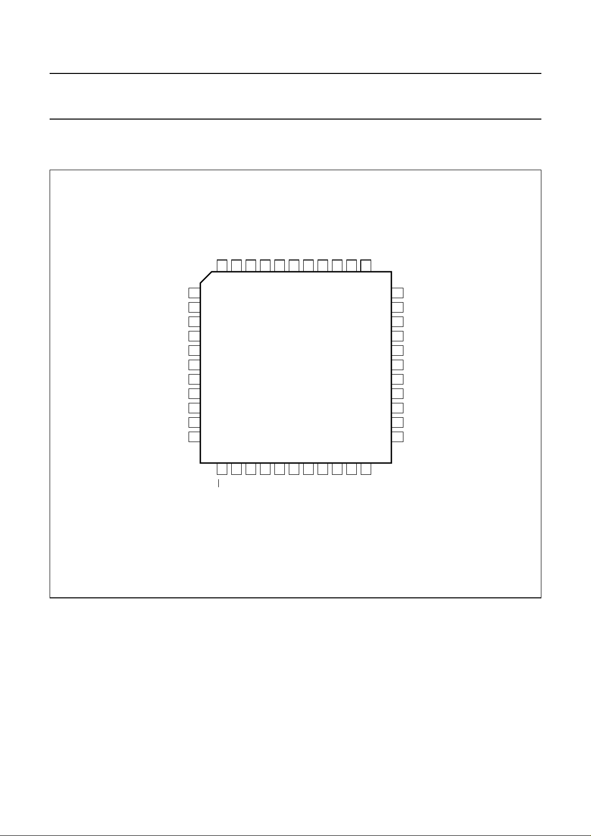
5 PINNING INFORMATION
5.1 Pinning
handbook, full pagewidth
P1.6
P1.7/MDY
43
42
P1.5
P1.4
41
40
PCD3350AH
P2.1
P2.2
P2.3
DP0.0/RCO
DP0.1
DP0.2
DP0.3
DP0.4
DP0.5
RTC1
RTC2
P2.0
44
1
2
3
4
5
6
7
8
9
10
11
P1.3
39
PCD3350A
SS
DD
TONE
V
38
37
P1.1
V
P1.2
36
35
34
33
P1.0
P0.7
32
31
P0.6
30
P0.5
P0.4
29
28
XTAL2
XTAL1
27
P0.3
26
P0.2
25
24
P0.1
P0.0
23
12
13
14
15
16
T1
CE/T0
DP1.0
RESET
DP1.1
Fig.2 Pin configuration.
17
DP1.2
18
DP1.3
19
DP1.4
20
DP1.5
21
DP1.6
22
MED264
DP1.7/DCO
1996 Dec 18 5
Page 6

Philips Semiconductors Product specification
8-bit microcontroller with DTMF generator,
PCD3350A
256 bytes EEPROM and real-time clock
5.2 Pin description
Table 1 SOT205-1 package (for information on parallel I/O ports, see Chapter 14)
SYMBOL PIN TYPE DESCRIPTION
P2.1 to P2.3 1 to 3 I/O 3 bits of Port 2: 4-bit quasi-bidirectional I/O port
DP0.0/RCO 4 I/O 1 bit of Derivative Port 0: 6-bit quasi-bidirectional I/O port; or RTC output
DP0.1 to DP0.5 5 to 9 I/O 5 bits of Derivative Port 0: 6-bit quasi-bidirectional I/O port
RTC1 10 I Real Time Clock 32 kHz oscillator input
RTC2 11 O Real Time Clock 32 kHz oscillator output
CE/
T0 12 I Chip Enable or Test 0 input
T1 13 I Test 1/count input of 8-bit Timer/event counter 1
RESET 14 I reset input
DP1.0 to DP1.6 15 to 21 I/O 7 bits of Derivative Port 1: 8-bit quasi-bidirectional I/O port
DP1.7/DCO 22 I/O 1 bit of Derivative Port 1: 8-bit quasi-bidirectional I/O port; or DTMF clock
output
P0.0 to P0.3 23 to 26 I/O 4 bits of Port 0: 8-bit quasi-bidirectional I/O port
XTAL1 27 I crystal oscillator/external clock input
XTAL2 28 O crystal oscillator output
P0.4 to P0.7 29 to 32 I/O 4 bits of Port 0: 8-bit quasi-bidirectional I/O port
P1.0 to P1.2 33 to 35 I/O 3 bits of Port 1: 8-bit quasi-bidirectional I/O port
V
SS
TONE 37 O DTMF output
V
DD
P1.3 to P1.6 39 to 42 I/O 4 bits of Port 1: 8-bit quasi-bidirectional I/O port
P1.7/MDY 43 I/O 1 bit of Port 1: 8-bit quasi-bidirectional I/O port; or melody output
P2.0 44 I/O 1 bit of Port 2: 4-bit quasi-bidirectional I/O port
36 P ground
38 P positive supply voltage
1996 Dec 18 6
Page 7

Philips Semiconductors Product specification
8-bit microcontroller with DTMF generator,
PCD3350A
256 bytes EEPROM and real-time clock
6 FREQUENCY GENERATOR
A versatile frequency generator section with built-in
programmable clock divider is provided (see Fig.3).
The clock divider allows the DTMF section to run either
with the main clock frequency (f
of it (f
DTMF
=1⁄3× f
) depending on the state of the divider
xtal
DTMF=fxtal
) or with a third
control bit DIV3 (see Table 4). The frequency generator
includes precision circuitry for dual tone multifrequency
(DTMF) signals, which is typically used for tone dialling
telephone sets.
6.1 Frequency generator derivative registers
6.1.1 H
IGH AND LOW GROUP FREQUENCY REGISTERS
Table 2 gives the addresses, symbols and access types of the High Group Frequency (HGF) and Low Group Frequency
(LGF) registers, used to set the frequency output.
Table 2 Hexadecimal addresses, symbols, access types and bit symbols of the frequency registers
REGISTER
ADDRESS
REGISTER
SYMBOL
ACCESS
TYPE
7 6 5 4 3 2 1 0
11H HGF W H7H6H5H4H3H2H1H0
12H LGF W L7L6L5L4L3L2L1L0
The TONE output can alternatively issue twelve modem
frequencies for data rates between 300 and 1200 bits/s.
In addition to DTMF and modem frequencies, two octaves
of musical scale in steps of semitones are available. Their
frequencies are provided either in purely sinusoidal form
on the TONE output or as a square wave on the port line
P1.7/MDY. The latter is typically for ringer applications in
telephone sets. If no frequency output is selected the
TONE output is in 3-state mode.
BIT SYMBOLS
6.1.2 CLOCK AND MELODY CONTROL REGISTER (MDYCON)
Table 3 Clock and Melody Control Register, MDYCON (address 13H; access type R/W)
7 6 5 4 3 2 1 0
00000EDCO DIV3 EMO
Table 4 Description of MDYCON bits
BIT SYMBOL DESCRIPTION
7to3 − These bits are set to a logic 0.
2 EDCO Enable DTMF clock output. If bit EDCO = 0, then DP1.7/DCO is a general purpose
derivative port line. If bit EDCO = 1, then DP1.7/DCO is the DTMF clock output.
EDCO = 1 does not inhibit the port instructions for DP1.7/DCO. Therefore the state of
both port line and flip-flop may be read in and the port flip-flop may be written by
derivative port instructions. However, the port flip-flop of DP1.7/DCO must remain set to
avoid conflicts between DTMF clock and port outputs.
1 DIV3 Enable DTMF clock divider. If bit DIV3 = 0, then the DTMF clock f
If bit DIV3 = 1, then f
DTMF
=1⁄3× f
xtal
.
DTMF=fxtal
.
0 EMO Enable Melody Output. If bit EMO = 0, then P1.7/MDY is a standard port line.
If bit EMO = 1, then P1.7/MDY is the melody output. EMO = 1 does not inhibit the port
instructions for P1.7/MDY. Therefore the state of both port line and flip-flop may be read
in and the port flip-flop may be written by port instructions. However, the port flip-flop of
P1.7/MDY must remain set to avoid conflicts between melody and port outputs.
When the HGF contents are zero while EMO = 1, P1.7/MDY is in the HIGH state.
1996 Dec 18 7
Page 8

Philips Semiconductors Product specification
8-bit microcontroller with DTMF generator,
256 bytes EEPROM and real-time clock
handbook, full pagewidth
8
8
8
INTERNAL BUS
8
f
xtal
CLOCK AND MELODY
CONTROL REGISTER
HGF REGISTER
LGF REGISTER
CLOCK
DIVIDER
DIGITAL
SINE WAVE
SYNTHESIZER
SWITCHED
CAPACITOR
BANDGAP
VOLTAGE
REFERENCE
DIGITAL
SINE WAVE
SYNTHESIZER
f
square wave
DAC
DAC
DTMF
SWITCHED
CAPACITOR
LOW-PASS
FILTER
PCD3350A
PORT/CLOCK
OUTPUT LOGIC
PORT/MELODY
OUTPUT LOGIC
RC LOW-PASS
FILTER
MGB782
DP1.7/
DCO
P1.7/
MDY
TONE
Fig.3 Block diagram of the frequency generator, melody output (P1.7/MDY) and DTMF clock output
(DP1.7/DCO).
6.2 Melody output (P1.7/MDY)
The melody output (P1.7/MDY) is very useful for
generating musical notes when a purely sinusoidal signal
is not required, such as for ringer applications.
The square wave (duty cycle =12⁄23 or 52%) will include
the attenuated harmonics of the base frequency, which is
defined by the contents of the HGF register (Table 2).
However, even higher frequency notes may be produced
since the low-pass filtering on the TONE output is not
applied to the P1.7/MDY output. This results in the
minimum decimal value x in the HGF register (see
equation in Section 6.4) being 2 for the P1.7/MDY output,
rather than 60 for the TONE output. A sinusoidal TONE
output is produced at the same time as the melody square
wave, but due to the filtering, the higher frequency sine
waves produced when x < 60 will not appear at the TONE
output.
Since the melody output is shared with P1.7, the port
flip-flop of P1.7 has to be set HIGH before using the
6.3 DTMF clock divider and output (DP1.7/DCO)
The DTMF clock divider allows the DTMF part to run either
with the main clock frequency (f
of it (f
DTMF
=1⁄3× f
) depending on the state of the divider
xtal
DTMF=fxtal
control bit DIV3 in register MDYCON.
For low power applications, a 3.58 MHz quartz crystal or
PXE resonator can be chosen together with the
divide-by-one function of the clock divider.
For other applications a 10.74 MHz quartz crystal or PXE
resonator may be chosen together with the divide-by-three
function of the clock divider. This triples the program speed
of the microcontroller, thereby keeping the assumed
DTMF frequency of 3.58 MHz.
Since a 3.58 MHz clock is needed for peripheral telephony
circuits such as the analog voice scrambler/descrambler
PCD4440T, a switchable DTMF clock output is provided
depending on the state of the enable clock output bit
EDCO in register MDYCON.
melody output. This is to avoid conflicts between melody
and port outputs. The melody output drive depends on the
configuration of port P1.7/MDY, see Chapter 14, Table 27.
) or with a third
1996 Dec 18 8
Page 9

Philips Semiconductors Product specification
-
8-bit microcontroller with DTMF generator,
256 bytes EEPROM and real-time clock
If EDCO = 1 and DIV3 = 1 in the MDYCON register: a
square wave with the frequency f
on the derivative port line DP1.7/DCO. If EDCO = 1 and
DIV3 = 0: a square wave with the frequency f
output on the derivative port line DP1.7/DCO.
The melody output drive depends on the configuration of
port P1.7/MDY, see Chapter 14, Table 27.
6.4 Frequency registers
The two frequency registers HGF and LGF define two
frequencies. From these, the digital sine synthesizers
together with the Digital-to-Analog Converters (DACs)
construct two sine waves. Their amplitudes are precisely
scaled according to the bandgap voltage reference. This
ensures tone output levels independent of supply voltage
and temperature. The amplitude of the Low Group
Frequency sine wave is attenuated by 2 dB compared to
the amplitude of the High Group Frequency sine wave.
The two sine waves are summed and then filtered by an
on-chip switched capacitor and RC low-pass filters.
These guarantee that all DTMF tones generated fulfil the
CEPT recommendations with respect to amplitude,
frequency deviation, total harmonic distortion and
suppression of unwanted frequency components.
The value 00H in a frequency register stops the
corresponding digital sine synthesizer. If both frequency
registers contain 00H, the whole frequency generator is
shut off, resulting in lower power consumption.
The frequency ‘f’ of the sine wave generated from either of
the frequency registers is a function of the clock frequency
’ and the decimal value ‘x’ held in the register.
‘f
xtal
The equation relating these variables is:
f
f
=
The frequency limitation given by x ≥ 60 is due to the
low-pass filters which would attenuate higher frequency
sine waves.
6.5 DTMF frequencies
Assuming an oscillator frequency f
DTMF standard frequencies can be implemented as
shown in Table 5.
xtal
-------------------------------23 x 2+()[]
; where 60 ≤ x ≤ 255.
=1⁄3× f
DTMF
= 3.58 MHz, the
xtal
is output
xtal
DTMF=fxtal
is
PCD3350A
The relationships between telephone keyboard symbols,
DTMF frequency pairs and the frequency register contents
are given in Table 6.
Table 5 DTMF standard frequencies and their
implementation; value = LGF, HGF contents
VALUE
(HEX)
DD 697 697.90 0.13 0.90
C8 770 770.46 0.06 0.46
B5 852 850.45 −0.18 −1.55
A3 941 943.23 0.24 2.23
7F 1209 1206.45 −0.21 −2.55
72 1336 1341.66 0.42 5.66
67 1477 1482.21 0.35 5.21
5D 1633 1638.24 0.32 5.24
Table 6 Dialling symbols, corresponding DTMF
TELEPHONE
KEYBOARD
SYMBOLS
0 (941, 1336) A3 72
1 (697, 1209) DD 7F
2 (697, 1336) DD 72
3 (697, 1477) DD 67
4 (770, 1209) C8 7F
5 (770, 1336) C8 72
6 (770, 1477) C8 67
7 (852, 1209) B5 7F
8 (852, 1336) B5 72
9 (852, 1477) B5 67
A (697, 1633) DD 5D
B (770, 1633) C8 5D
C (852, 1633) B5 5D
D (941, 1633) A3 5D
• (941, 1209) A3 7F
# (941, 1477) A3 67
FREQUENCY (Hz) DEVIATION
STANDARD GENERATED (%) (Hz)
frequency pairs and frequency register contents
DTMF FREQ.
PAIRS
(Hz)
LGF
VALUE
(HEX)
HGF
VALUE
(HEX)
1996 Dec 18 9
Page 10

Philips Semiconductors Product specification
8-bit microcontroller with DTMF generator,
256 bytes EEPROM and real-time clock
6.6 Modem frequencies
Again assuming an oscillator frequency f
the standard modem frequencies can be implemented as
in Table 7. It is suggested to define the frequency by the
HGF register while the LGF register contains 00H,
disabling Low Group Frequency generation.
Table 7 Standard modem frequencies and their
implementation
HGF
FREQUENCY (Hz) DEVIATION
VALUE
(HEX)
9D 980
82 1180
8F 1070
79 1270
80 1200
45 2200
76 1300
48 2100
5C 1650
52 1850
4B 2025
44 2225
MODEM GENERATED (%) (Hz)
(1)
(1)
(2)
(2)
(3)
(3)
(4)
(4)
(1)
(1)
(2)
(2)
978.82 −0.12 −1.18
1179.03 −0.08 −0.97
1073.33 0.31 3.33
1265.30 −0.37 −4.70
1197.17 −0.24 −2.83
2192.01 −0.36 −7.99
1296.94 −0.24 −3.06
2103.14 0.15 3.14
1655.66 0.34 5.66
1852.77 0.15 2.77
2021.20 −0.19 −3.80
2223.32 −0.08 −1.68
Notes
1. Standard is V.21.
2. Standard is Bell 103.
3. Standard is Bell 202.
4. Standard is V.23.
6.7 Musical scale frequencies
= 3.58 MHz,
xtal
PCD3350A
Table 8 Musical scale frequencies and their
implementation
HGF
NOTE
VALUE
(HEX)
D#5 F8 622.3 622.5
E5 EA 659.3 659.5
F5 DD 698.5 697.9
F#5 D0 740.0 741.1
G5 C5 784.0 782.1
G#5 B9 830.6 832.3
A5 AF 880.0 879.3
A#5 A5 923.3 931.9
B5 9C 987.8 985.0
C6 93 1046.5 1044.5
C#6 8A 1108.7 1111.7
D6 82 1174.7 1179.0
D#6 7B 1244.5 1245.1
E6 74 1318.5 1318.9
F6 6D 1396.9 1402.1
F#6 67 1480.0 1482.2
G6 61 1568.0 1572.0
G#6 5C 1661.2 1655.7
A6 56 1760.0 1768.5
A#6 51 1864.7 1875.1
B6 4D 1975.5 1970.0
C7 48 2093.0 2103.3
C#7 44 2217.5 2223.3
D7 40 2349.3 2358.1
D#7 3D 2489.0 2470.4
FREQUENCY (Hz)
STANDARD
(1)
GENERATED
Finally, two octaves of musical scale in steps of semitones
can be realized, again assuming an oscillator frequency
f
= 3.58 MHz (Table 8). It is suggested to define the
xtal
frequency by the HGF register while the LGF contains
00H, disabling Low Group Frequency generation.
1996 Dec 18 10
Note
1. Standard scale based on A4 @ 440 Hz.
Page 11

Philips Semiconductors Product specification
8-bit microcontroller with DTMF generator,
256 bytes EEPROM and real-time clock
7 EEPROM AND TIMER 2 ORGANIZATION
The PCD3350A has 256 bytes of Electrically Erasable
Programmable Read Only Memory (EEPROM). Such
non-volatile storage provides data retention without the
need for battery backup. In telecom applications, the
EEPROM is used for storing redial numbers and for short
dialling of frequently used numbers. More generally,
EEPROM may be used for customizing microcontrollers,
such as to include a PIN code or a country code, to define
trimming parameters, to select application features from
the range stored in ROM.
The most significant difference between a RAM and an
EEPROM is that a bit in EEPROM, once written to a
logic 1, cannot be cleared by a subsequent write
operation. Successive write accesses actually perform a
logical OR with the previously stored information.
Therefore, to clear a bit, the whole byte must be erased
and re-written with the particular bit cleared. Thus, an
erase-and-write operation is the EEPROM equivalent of a
RAM write operation.
PCD3350A
Whereas read access times to an EEPROM are
comparable to RAM access times, write and erase access
times are much slower at 5 ms each. To make these
operations more efficient, several provisions are available
in the PCD3350A.
First, the EEPROM array is structured into 64 four-byte
pages (see Fig.4) permitting access to 4 bytes in parallel
(write page, erase/write page and erase page). It is also
possible to erase and write individual bytes.
Finally, the EEPROM address register provides
auto-incrementing, allowing very efficient read and write
accesses to sequential bytes.
To simplify the erase and write timing, the derivative 8-bit
down-counter (Timer 2) with reload register is provided.
In addition to EEPROM timing, Timer 2 can be used for
general real-time tasks, such as for measuring signal
duration and for defining pulse widths.
1996 Dec 18 11
Page 12

Philips Semiconductors Product specification
8-bit microcontroller with DTMF generator,
256 bytes EEPROM and real-time clock
handbook, full pagewidth
8
EEPROM ADDRESS REGISTER
2
2 : 4 DECODER
EEPROM LATCH 0
8
F0
F1EEPROM LATCH 1
F2EEPROM LATCH 2
F3EEPROM LATCH 3
PCD3350A
6
6 : 64 DECODER
256-byte EEPROM ARRAY
(64 4-byte PAGES)
8
INTERNAL
BUS
8
8
8
8
8
EEPROM TEST REGISTER
EEPROM CONTROL REGISTER
TIMER 2 RELOAD REGISTER
8
TIMER 2 REGISTER (T2)
1
f
xtal
480
MGB783
T2F set on
underflow
Fig.4 Block diagram of the EEPROM and Timer 2.
1996 Dec 18 12
Page 13

Philips Semiconductors Product specification
8-bit microcontroller with DTMF generator,
PCD3350A
256 bytes EEPROM and real-time clock
7.1 EEPROM registers
7.1.1 EEPROM C
The behaviour of the EEPROM and Timer 2 section is defined by the EEPROM Control Register, as detailed in Tables
9, 10 and 11.
Table 9 EEPROM Control Register, EPCR (address 04H, access type R/W)
76543210
STT2 ET2I T2F EWP MC3 MC2 MC1 0
Table 10 Description of EPCR bits
BIT SYMBOL DESCRIPTION
7 STT2 Start T2. If STT2 = 0, then Timer 2 is stopped; T2 value held. If STT2 = 1, then T2
6 ET2I Enable T2 interrupt. If ET2I = 0, then T2F event cannot request interrupt. If ET2I = 1,
5 T2F Timer 2 flag. Set when T2 underflows (or by program); reset by program.
4 EWP Erase or write in progress (EWP). Set by program (EWP starts EEPROM erase and/or
3 MC3 Mode control 3 to 1. These three bits in conjunction with bit EWP select the mode as
2 MC2
1 MC1
0 − This bit is set to a logic 0.
ONTROL REGISTER (EPCR)
decrements from reload value.
then T2F event can request interrupt.
write and Timer 2). Reset at the end of EEPROM erase and/or write.
shown in Table 11.
Table 11 Mode selection; X = don’t care
EWP MC3 MC2 MC1 DESCRIPTION
0 0 0 0 read byte
0 0 1 0 increment mode
1 0 1 X write page
1 1 0 0 erase/write page
1 1 1 1 erase page
X 0 0 1 not allowed
X101
X110
1996 Dec 18 13
Page 14

Philips Semiconductors Product specification
8-bit microcontroller with DTMF generator,
PCD3350A
256 bytes EEPROM and real-time clock
7.1.2 EEPROM ADDRESS REGISTER (ADDR)
The EEPROM Address Register (ADDR) determines the EEPROM location to which an EEPROM access is directed.
As a whole, ADDR auto-increments after read and write cycles to EEPROM, but remains fixed after erase cycles. This
behaviour generates the correct ADDR contents for sequential read accesses and for sequential write or erase/write
accesses with intermediate page setup. Overflow of the 8-bit counter wraps around to zero. See Tables 12 and 13.
Table 12 EEPROM Address Register, ADDR (address 01H, access type R/W)
76543210
AD7 AD6 AD5 AD4 AD3 AD2 AD1 AD0
Table 13 Description of ADDR bits
BIT SYMBOL DESCRIPTION
7 to 2 AD7 to AD2 AD7 to AD2 select one of 64 pages.
1 to 0 AD1 to AD0 AD1 and AD0 are irrelevant during erase and write cycles. For read accesses, AD0 and
AD1 indicate the byte location within an EEPROM page. During page setup, finally, AD0
and AD1 select EEPROM Latch 0 to 3 whereas AD2 to AD6 are irrelevant. If increment
mode (see Table 11) is active during page setup, the subcounter consisting of AD0 and
AD1 increments after every write to an EEPROM latch, thus enhancing access to
sequential EEPROM latches. Incrementing stops when EEPROM Latch 3 is reached,
i.e. when AD0 and AD1 are both a logic 1.
7.1.3 EEPROM D
Table 14 EEPROM Data Register, DATR (address 03H; access type R/W)
76543210
D7 D6 D5 D4 D3 D2 D1 D0
Table 15 Description of DATR bits
BIT SYMBOL DESCRIPTION
7 to 0 D7 to D0 The EEPROM Data Register (DATR) is only a conceptual entity. A read operation from
7.1.4 EEPROM
The EEPROM Test Register is used for testing purposes during device manufacture. It must not be accessed by the
device user.
ATA REGISTER (DATR)
DATR, reads out the EEPROM byte addressed by ADDR. On the other hand, a write
operation to DATR, loads data into the EEPROM latch (see Fig.4) defined by bits AD0
and AD1 of ADDR.
TEST REGISTER (TST)
1996 Dec 18 14
Page 15

Philips Semiconductors Product specification
8-bit microcontroller with DTMF generator,
256 bytes EEPROM and real-time clock
7.2 EEPROM latches
The four EEPROM latches (EEPROM Latch 0 to 3; Fig.4)
cannot be read by user software. Due to their construction,
the latches can only be preset, but not cleared. Successive
write operations through DATR to the EEPROM latches
actually perform a logical OR with the previously stored
data in EEPROM. The EEPROM latches are reset at the
conclusion of any EEPROM cycle.
7.3 EEPROM flags
The four EEPROM flags (F0 to F3; Fig.4) cannot be
directly accessed by user software. An EEPROM flag is
set as a side-effect when the corresponding EEPROM
latch is written through DATR. The EEPROM flags are
reset at the conclusion of any EEPROM cycle.
7.4 EEPROM macros
The instruction sequence used in an EEPROM access
should be treated as an indivisible entity. Erroneous
programs result if ADDR, DATR, RELR or EPCR are
inadvertently changed during an EEPROM cycle or its
setup. Special care should be taken if the program may
asynchronously divert due to an interrupt. A new access to
the EEPROM may only be initiated when no write, erase or
erase/write cycles are in progress. This can be verified by
reading bit EWP (register EPCR).
For write, erase and erase/write cycles, it is assumed that
the Timer 2 Reload Register (RELR) has been loaded with
the appropriate value for a 5 ms delay, which depends on
(see Table 22). The end of a write, erase or erase/write
f
xtal
cycle will be signalled by a cleared EWP and by a Timer 2
interrupt provided that ET2I = 1 and that the derivative
interrupt is enabled.
7.5 EEPROM access
One read, one write, one erase/write and one erase
access are defined by bits EWP and MC1 to MC3 in the
EPCR register; see Table 9.
Read byte retrieves the EEPROM byte addressed by
ADDR when DATR is read. Read cycles are
instantaneous.
Write and erase cycles take 5 ms, however. Erase/write is
a combination of an erase and a subsequent write cycle,
consequently taking 10 ms.
As their names imply, write page, erase page and
erase/write page are applied to a whole EEPROM page.
Therefore, bits AD0 and AD1 of register ADDR (see
Table 12), defining the byte location within an EEPROM
PCD3350A
page, are irrelevant during write and erase cycles.
However, write and erase cycles need not affect all bytes
of the page. The EEPROM flags F0 to F3 (see Fig.4)
determine which bytes within the EEPROM page are
affected by the erase and/or write cycles. A byte whose
corresponding EEPROM flag is zero remains unchanged.
With erase page, a byte is erased if its corresponding
EEPROM flag is set. With write page, data in EEPROM
Latch 0 to 3 (Fig.4) are ORed to the individual page bytes
if and only if the corresponding EEPROM flags are set.
In an erase/write cycle, F0 to F3 select which page bytes
are erased and ORed with the corresponding EEPROM
latches. ORing, in this case, means that the EEPROM
latches are copied to the selected page bytes.
The described page-wise organization of erase and write
cycles allows up to four bytes to be individually erased or
written within 5 ms. This advantage necessitates a
preparation step, called page setup, before the actual
erase and/or write cycle can be executed.
Page setup controls EEPROM latches and EEPROM
flags. This will be described in the Sections 7.5.1 to 7.5.5.
7.5.1 P
Page setup is a preparation step required before write
page, erase page and erase/write page cycles.
As previously described, these page operations include
single-byte write, erase and erase/write as a special case.
EEPROM flags F0 to F3 determine which page bytes will
be affected by the mentioned page operations. EEPROM
Latch 0 to 3 must be preset through DATR to specify the
write cycle data to EEPROM and to set the EEPROM flags
as a side-effect.
Obviously, the actual preset value of the EEPROM latches
is irrelevant for erase page. Preset of one, two, three or all
four EEPROM latches and the corresponding EEPROM
flags can be performed by repeatedly defining ADDR and
writing to DATR (see Table 16).
If more than one EEPROM latch must be preset, the
subcounter consisting of AD0 and AD1 can be induced to
auto-increment after every write to DATR, thus stepping
through all EEPROM latches. For this purpose, increment
mode (Table 11) must be selected. Auto-incrementing
stops at EEPROM Latch 3. It is not mandatory to start at
EEPROM Latch 0 as in shown in Table 17.
Note that AD2 to AD7 are irrelevant during page setup.
They will usually specify the intended EEPROM page,
anticipating the subsequent page cycle.
AGE SETUP
1996 Dec 18 15
Page 16

Philips Semiconductors Product specification
8-bit microcontroller with DTMF generator,
256 bytes EEPROM and real-time clock
From now on, it will be assumed that AD2 to AD7 will
contain the intended EEPROM page address after page
setup.
Table 16 Page setup; preset
INSTRUCTION RESULT
MOV A, #addr address of EEPROM latch
MOV ADDR, A send address to ADDR
MOV A, #data load write, erase/write or erase
data
MOV DA TR, A send data to addressed EEPROM
latch
Table 17 Page setup; auto-incrementing
INSTRUCTION RESUL T
MOV A, #MC2 increment mode control word
MOV EPCR, A select increment mode
MOV A, #baddr EEPROM Latch0 address
(AD0 = AD1 = 0)
MOV ADDR, A send EEPROM Latch 0 address
to ADDR
MOV A, R0 load 1stbyte from Register 0
Latch 1
Latch 2
st
byte to EEPROM Latch 0
nd
byte from Register 1
nd
byte to EEPROM
rd
byte from Register 2
rd
byte to EEPROM
th
byte from Register 3
th
byte to EEPROM Latch 3
MOV DA TR, A send 1
MOV A, R1 load 2
MOV DATR, A send 2
MOV A, R2 load 3
MOV DATR, A send 3
MOV A, R3 load 4
MOV DA TR, A send 4
7.5.2 R
EAD BYTE
Since ADDR auto-increments after a read cycle regardless
of the page boundary, successive bytes can efficiently be
read by repeating the last instruction.
Table 18 Read byte
INSTRUCTION RESULT
MOV A, #RDADDR load read address
MOV ADDR, A send address to ADDR
MOV A, DATR read EEPROM data
PCD3350A
7.5.3 WRITE PAGE
The write cycle performs a logical OR between the data in
the EEPROM latches and that in the addressed EEPROM
page. To actually copy the data from the EEPROM
latches, the corresponding bytes in the page should
previously have been erased.
The EEPROM latches are preset as described in
Section 7.5.1. The actual transfer to the EEPROM is then
performed as shown in Table 19.
The last instruction also starts Timer 2. The data in the
EEPROM latches are ORed with that in the corresponding
page bytes within 5 ms. A single-byte write is simply a
special case of ‘write page’.
ADDR auto-increments after the write cycle. If AD0 and
AD1 addressed EEPROM Latch 3 prior to the write cycle,
ADDR will point to the next EEPROM page (by bits AD2
to AD7) and to EEPROM Latch 0 (by bits AD0 and AD1).
This allows efficient coding of multi-page write operations.
Table 19 Write page
INSTRUCTION RESULT
MOV A, #EWP + MC2 ‘write page’ control word
MOV EPCR, A start ‘write page’ cycle
7.5.4 E
The EEPROM latches are preset as described in
Section 7.5.1. The page bytes corresponding to the
asserted flags (among F0 to F3) are erased and re-written
with the contents of the respective EEPROM latches.
The last instruction also starts Timer 2. Erasure takes
5 ms upon which Timer Register T2 reloads for another
5 ms cycle for writing. The top cycles together take 10 ms.
A single-byte erase/write is simply a special case of
‘erase/write page’.
ADDR auto-increments after the write cycle. If AD0 and
AD1 addressed EEPROM Latch 3 prior to the write cycle,
ADDR will point to the next EEPROM page (by AD2 to
AD7) and to EEPROM Latch 0 (by AD0 and AD1). This
allows efficient coding of multi-page erase/write
operations.
Table 20 Erase/write page
MOV A, #EWP + MC3 ‘erase/write page’ control word
MOV EPCR, A start ‘erase/write page’ cycle
RASE/WRITE PAGE
INSTRUCTION RESULT
1996 Dec 18 16
Page 17

Philips Semiconductors Product specification
8-bit microcontroller with DTMF generator,
256 bytes EEPROM and real-time clock
7.5.5 ERASE PAGE
The EEPROM flags are set as described in Section 7.5.1.
The corresponding page bytes are erased.
The last instruction also starts Timer 2. Erasure takes
5 ms. A single-byte erase is simply a special case of
‘erase page’.
Note that ADDR does not auto-increment after an erase
cycle.
Table 21 Erase page
INSTRUCTION RESULT
MOV A, #EWP + MC3 + MC2 + MC1 ‘erase page’
control word
MOV EPCR, A start ‘erase
page’ cycle
7.6 Timer 2
Timer 2 is a 8-bit down-counter decremented at a rate of
1
⁄
× f
480
a general purpose timer. Conflicts between the two
applications should be carefully avoided.
7.6.1 T
When used for EEPROM timing, Timer 2 serves to
generate the 5 ms intervals needed for erasing or writing
the EEPROM. At the decrement rate of1⁄
reload value for a 5 ms interval is a function of f
Table 22 summarizes the required reload values for a
number of oscillator frequencies.
Timer 2 is started by setting bit EWP in the EPCR.
The Timer Register T2 is loaded with the reload value from
RELR. T2 decrements to zero.
. It may be used either for EEPROM timing or as
xtal
IMER 2 FOR EEPROM TIMING
× f
xtal
xtal
, the
480
.
PCD3350A
The second underflow of an erase/write cycle and the first
underflow of write page and erase page conclude the
corresponding EEPROM cycle. Timer 2 is stopped, T2F is
set whereas EWP and MC1 to MC3 are cleared.
Table 22 Reload values as a function of f
f
xtal
(MHz)
RELOAD VALUE
(HEX)
10A
214
3.58 25
63E
10.74 6F
16 A6
Note
1. The reload value is (5 × 10−3×1⁄
f
in MHz.
xtal
7.6.2 T
IMER 2 AS A GENERAL PURPOSE TIMER
When used for purposes other than EEPROM timing,
Timer 2 is started by setting STT2. The Timer 2 Register
T2 (see Table 28) is loaded with the reload value from
RELR. T2 decrements to zero. On underflow, T2 is
reloaded from RELR, T2F is set and T2 continues to
decrement.
Timer 2 can be stopped at any time by clearing STT2.
The value of T2 is then held and can be read out. After
setting STT2 again, Timer 2 decrements from the reload
value. Alternatively, it is possible to read T2 ‘on the fly’ i.e.
while Timer 2 is operating.
480
× f
xtal
(1)
xtal
) − 1;
For an erase/write cycle, underflow of T2 indicates the end
of the erase operation. Therefore, Timer Register T2 is
reloaded from RELR for another 5 ms interval during
which the flagged EEPROM latches are copied to the
corresponding bytes in the page addressed by ADDR.
1996 Dec 18 17
Page 18

Philips Semiconductors Product specification
8-bit microcontroller with DTMF generator,
256 bytes EEPROM and real-time clock
8 REAL-TIME CLOCK
The Real Time Clock (RTC) consists of a 32 kHz crystal
oscillator, a 32 kHz to 1 second or 1 minute divider chain,
an 8-bit Frequency Adjustment Register and the Clock
Control Register. The complete RTC section works
independently of the microcontroller status, even in Idle
and Stop mode.
8.1 Oscillator
The internal 32 kHz oscillator needs an external quartz
crystal with a frequency of 32768.00 Hz (a positive
deviation up to +259 × 10
feedback resistor between pins RTC1 and RTC2; 4.7 MΩ
is recommended. It is controlled by the RUN-bit in the
Clock Control Register.
8.2 Divider chain
The divider chain operates with the 32 kHz oscillator
output and divides this signal down to two clocks with a
period of 1 second or 1 minute. Depending on bit ITS in the
Clock Control Register, the falling edge of the seconds or
minutes clock is used to set the Clock Interrupt Flag (CIF)
in the Clock Control Register.
−6
is allowed) and an external
PCD3350A
Since the clock interrupt is used to let the microcontroller
leave the Stop mode, it is ORed to the external interrupt
T0) and has the same functionality, e.g. it must be
(CE/
enabled in the Clock Control Register (bit ECI) and by
execution of the instruction ‘EN I’. The clock interrupt will
then be treated as an external interrupt.
Additionally, the divider chain generates a 16 kHz clock
(RCO) that can be routed through derivative port line
DP0.0/RCO, controlled by bit ERCO in the Clock Control
Register.
8.3 Frequency adjustment
The frequency adjustment is used to extend the interrupt
time by defining the number of 16 kHz clocks in the
Frequency Adjustment Register that will be counted twice
within the first second period after a minute interrupt.
If the second interrupt is used (ITS = 1), every 60
may be up to 15.3 ms longer than the others as a result of
the frequency adjustment. The adjusted Minute Interrupt
Time (MIT) now shows a maximum deviation of 0.5 × 10⁻⁶.
th
interval
1996 Dec 18 18
Page 19

Philips Semiconductors Product specification
8-bit microcontroller with DTMF generator,
PCD3350A
256 bytes EEPROM and real-time clock
8.4 Real-time clock derivative registers
8.4.1 C
The register access type is R/W and the value at reset is 00H.
Table 23 Clock Control Register, CLCR (address 20H)
Table 24 Description of CLCR bits
LOCK CONTROL REGISTER (CLCR)
76543210
0 TST2 TST1 ERCO RUN ITS CIF ECI
BIT SYMBOL DESCRIPTION
7 − This bit is set to a logic 0.
6 TST2 Test 2 input. This is a testing bit; has to be fixed at a logic 0 by user software.
5 TST1 Test 1 input. This is a testing bit; has to be fixed at a logic 0 by user software.
4 ERCO Enable 16 kHz clock output. If ERCO = 0, then the DP0.0/RCO is a derivative port line.
If ERCO = 1, then DP0.0./RCO is a 16 kHz clock output. ERCO = 1 does not inhibit the
port instructions for DP0.0/RCO. Therefore the state of both port line and flip-flop may
be read in and the port flip-flop may be written by derivative port instructions. However,
the port flip-flop of DP0.0/RCO must remain set to avoid conflicts between 16 kHz clock
and port outputs.
3 RUN Clock run or stop bit. If RUN = 0, then the oscillator is stopped and the clock is reset.
If RUN = 1, then the oscillator and the clock are running.
2 ITS Interrupt Time Select. If ITS = 1, then the interrupt time is one second.
If ITS = 0, then the interrupt time is one minute.
1 CIF Clock Interrupt Flag. Set by hardware, if RTC divider chain overflows (every second or
minute depending on ITS) or by program. Reset by program.
0 ECI Enable Clock Interrupt. If ECI = 0, then CIF event cannot request interrupt.
If ECI = 1, then CIF event requests interrupt.
8.4.2 F
REQUENCY ADJUSTMENT REGISTER (FAR)
The frequency adjustment value of the RTC is defined by the 8-bit Frequency Adjustment Register. The register access
type is R/W. The value of FAR at reset is 00H.
The significance of the individual bits of FAR can be illustrated by the following equation:
14
------------
Minute Interrupt Time (MIT) 60 2
where f
= RTC frequency and ‘FAR’ is the decimal contents of the Frequency Adjustment Register.
RCO
Table 26 shows the recommended correction factor FAR for all allowed RTC frequencies f
f
×
RCO
+=
FAR
----------- -
14
2
RCO
.
Table 25 Frequency Adjustment Register, FAR (address 21H)
76543210
FAR7 FAR6 FAR5 FAR4 FAR3 FAR2 FAR1 FAR0
1996 Dec 18 19
Page 20

Philips Semiconductors Product specification
8-bit microcontroller with DTMF generator,
256 bytes EEPROM and real-time clock
Table 26 FAR as a result of f
f
RCO
16384.000 00
16384.018 01
16384.033 02
16384.051 03
16384.066 04
16384.084 05
16384.100 06
16384.117 07
16384.135 08
16384.150 09
16384.168 0A
16384.184 0B
16384.201 0C
16384.217 0D
16384.234 0E
16384.250 0F
16384.268 10
16384.283 11
16384.301 12
16384.316 13
16384.334 14
16384.350 15
16384.367 16
16384.385 17
16384.400 18
16384.418 19
16384.434 1A
16384.451 1B
16384.467 1C
16384.484 1D
RCO
FAR (HEX)
f
RCO
16384.500 1E
16384.518 1F
16384.533 20
16384.551 21
16384.566 22
16384.584 23
16384.600 24
16384.617 25
16384.635 26
16384.650 27
16384.668 28
16384.684 29
16384.701 2A
16384.717 2B
16384.734 2C
16384.750 2D
16384.768 2E
16384.783 2F
16384.801 30
16384.816 31
16384.834 32
16384.850 33
16384.867 34
16384.885 35
16384.900 36
16384.918 37
16384.934 38
16384.951 39
16384.967 3A
16384.984 3B
16385.000 3C
FAR (HEX)
PCD3350A
f
RCO
16385.018 3D
16385.033 3E
16385.051 3F
16385.066 40
16385.084 41
16385.100 42
16385.117 43
16385.135 44
16385.150 45
16385.168 46
16385.184 47
16385.201 48
16385.217 49
16385.234 4A
16385.250 4B
16385.268 4C
16385.283 4D
16385.301 4E
16385.316 4F
16385.334 50
16385.350 51
16385.367 52
16385.385 53
16385.400 54
16385.418 55
16385.434 56
16385.451 57
16385.467 58
16385.484 59
16385.500 5A
16385.518 5B
FAR (HEX)
1996 Dec 18 20
Page 21

Philips Semiconductors Product specification
8-bit microcontroller with DTMF generator,
256 bytes EEPROM and real-time clock
f
RCO
16385.533 5C
16385.551 5D
16385.566 5E
16385.584 5F
16385.600 60
16385.617 61
16385.635 62
16385.650 63
16385.668 64
16385.684 65
16385.701 66
16385.717 67
16385.734 68
16385.750 69
16385.768 6A
16385.783 6B
16385.801 6C
16385.816 6D
16385.834 6E
16385.850 6F
16385.867 70
16385.885 71
16385.900 72
16385.918 73
16385.934 74
16385.951 75
16385.967 76
16385.984 77
FAR (HEX)
f
RCO
16386.000 78
16386.018 79
16386.033 7A
16386.051 7B
16386.066 7C
16386.084 7D
16386.100 7E
16386.117 7F
16386.135 80
16386.150 81
16386.168 82
16386.184 83
16386.201 84
16386.217 85
16386.234 86
16386.250 87
16386.268 88
16386.283 89
16386.301 8A
16386.316 8B
16386.334 8C
16386.350 8D
16386.367 8E
16386.385 8F
16386.400 90
16386.418 91
16386.434 92
16386.451 93
FAR (HEX)
PCD3350A
f
RCO
16386.467 94
16386.484 95
16386.500 96
16386.518 97
16386.533 98
16386.551 99
16386.566 9A
16386.584 9B
16386.600 9C
16386.617 9D
16386.635 9E
16386.650 9F
16386.668 A0
16386.684 A1
16386.701 A2
16386.717 A3
16386.734 A4
16386.750 A5
16386.768 A6
16386.783 A7
16386.801 A8
16386.816 A9
16386.834 AA
16386.850 AB
16386.867 AC
16386.885 AD
16386.900 AE
16386.918 AF
FAR (HEX)
1996 Dec 18 21
Page 22

Philips Semiconductors Product specification
8-bit microcontroller with DTMF generator,
256 bytes EEPROM and real-time clock
f
RCO
16386.934 B0
16386.951 B1
16386.967 B2
16386.984 B3
16387.000 B4
16387.018 B5
16387.033 B6
16387.051 B7
16387.066 B8
16387.084 B9
16387.100 BA
16387.117 BB
16387.135 BC
16387.150 BD
16387.168 BE
16387.184 BF
16387.201 C0
16387.217 C1
16387.234 C2
16387.250 C3
16387.268 C4
16387.283 C5
16387.301 C6
16387.316 C7
16387.334 C8
16387.350 C9
16387.367 CA
FAR (HEX)
f
RCO
16387.385 CB
16387.400 CC
16387.418 CD
16387.434 CE
16387.451 CF
16387.467 D0
16387.484 D1
16387.500 D2
16387.518 D3
16387.533 D4
16387.551 D5
16387.566 D6
16387.584 D7
16387.600 D8
16387.617 D9
16387.635 DA
16387.650 DB
16387.668 DC
16387.684 DD
16387.701 DE
16387.717 DF
16387.734 E0
16387.750 E1
16387.768 E2
16387.783 E3
16387.801 E4
16387.816 E5
FAR (HEX)
PCD3350A
f
RCO
16387.834 E6
16387.850 E7
16387.867 E8
16387.885 E9
16387.900 EA
16387.918 EB
16387.934 EC
16387.951 ED
16387.967 EE
16387.984 EF
16388.002 F0
16388.018 F1
16388.035 F2
16388.051 F3
16388.068 F4
16388.084 F5
16388.102 F6
16388.117 F7
16388.135 F8
16388.152 F9
16388.168 FA
16388.186 FB
16388.201 FC
16388.219 FD
16388.234 FE
16384.000 FF
FAR (HEX)
1996 Dec 18 22
Page 23

Philips Semiconductors Product specification
8-bit microcontroller with DTMF generator,
256 bytes EEPROM and real-time clock
9 DERIVATIVE INTERRUPTS
One derivative interrupt event is defined. It is controlled by
bits T2F and ET2I in the EPCR (see Tables 9 and 10).
The derivative interrupt event occurs when T2F is set. This
request is honoured under the following circumstances:
• No interrupt routine proceeds
• No external interrupt request is pending
• The derivative interrupt is enabled
• ET2I is set.
The derivative interrupt routine must include instructions
that will remove the cause of the derivative interrupt by
explicitly clearing T2F. If the derivative interrupt is not
used, T2F may directly be tested by the program.
Obviously, T2F can also be asserted under program
control, e.g. to generate a software interrupt.
Although the clock interrupt is part of a derivative function
it is linked to the external interrupt. A clock interrupt
request is honoured under the following circumstances:
• No interrupt routine proceeds
• No external interrupt request is pending
• The enable clock interrupt bit in the derivative clock
control register is set.
10 TIMING
Although the PCD3350A operates over a clock frequency
range from 1 to 16 MHz, f
usually be chosen to take full advantage of the frequency
generator (DTMF) section.
= 3.58 MHz or 10.74 MHz will
xtal
PCD3350A
12 IDLE MODE
In Idle mode all derivative functions remain operative, i.e.:
• DTMF generator
• DTMF clock divider and output
• 32 kHz crystal oscillator and RTC
• EEPROM and Timer 2 sections.
13 STOP MODE
Since the oscillator is switched off, the frequency
generator, the EEPROM and the Timer 2 sections receive
no clock. It is suggested to clear both the HGF and the
LGF registers before entering Stop mode. This will cut off
the biasing of the internal amplifiers, considerably
reducing current requirements.
The Stop mode must not be entered while an erase
and/or write access to EEPROM is in progress. The STOP
instruction may only be executed when EWP in EPCR is
zero. The Timer 2 section is frozen during Stop mode.
After exit from Stop mode by a HIGH level on CE/
Timer 2 proceeds from the held state.
The 32 kHz crystal oscillator and the RTC section remain
operative during Stop mode (depending only on bit RUN in
the Clock Control Register). In addition to the description
in the
“PCD33xxA Family”
left by a clock interrupt event (see Chapter 9).
data sheet, Stop mode may be
T0,
11 RESET
In addition to the conditions given in the
Family”
the reset state.
1996 Dec 18 23
data sheet, all derivative registers are cleared in
“PCD33xxA
Page 24

Philips Semiconductors Product specification
8-bit microcontroller with DTMF generator,
PCD3350A
256 bytes EEPROM and real-time clock
14 SUMMARY OF I/O PORTS AND ROM MASK OPTIONS
All standard quasi-bidirectional I/O ports are available; see
• Port 0: 8 parallel port lines P0.0 to P0.7
• Port 1: 8 parallel port lines P1.0 to P1.7
• Port 2: 4 parallel port lines P2.0 to P2.3.
In addition to the standard ports, two derivative I/O ports are available:
• Derivative Port 0: 6 parallel port lines DP0.0 to DP0.5 (register DP0L)
• Derivative Port 1: 8 parallel port lines DP1.0 to DP1.7 (register DP1L).
The port options and the other ROM mask options are listed in Table 27. See Table 28 for the addresses of DP0L and
DP1L.
Table 27 ROM mask options
FUNCTION IMPLEMENTED IN ROM OPTION
Program/data Any mix of instructions and data up to ROM size of
Port Output
P0.0 to P0.7 standard open-drain push-pull
P1.0 to P1.6 standard open-drain push-pull
P1.7/MDY; note 1 standard open-drain push-pull
P2.0 to P2.3 standard open-drain push-pull
DP0.0 to DP0.5 standard open-drain push-pull
DP1.0 to DP1.6 standard open-drain push-pull
DP1.7/DCO; note 2 standard open-drain push-pull
“PCD33xxA Family”
8 kbytes.
data sheet.
Port State after reset
P0.0 to P0.7 set reset −
P1.0 to P1.6 set reset −
P1.7/MDY set reset −
P2.0 to P2.3 set reset −
DP0.0 to DP0.5 set reset −
DP1.0 to DP1.6 set reset −
DP1.7/DCO set reset −
Oscillator
Transconductance LOW (g
Power-on-reset
Power-on-reset voltage level: V
Notes
1. If standard (Option 1) or push-pull (Option 3) output is chosen, the P1.7/MDY output becomes a push-pull output.
If open-drain (Option 2) is chosen, the P1.7/MDY output becomes an open-drain output.
2. If standard (Option 1) or push-pull (Option 3) output is chosen, the DP1.7/DCO output becomes a push-pull output.
If open-drain (Option 2) is chosen, the DP1.7/DCO output becomes an open-drain output.
1996 Dec 18 24
POR
1.2 to 3.6 V in increments of 100 mV; OFF
) MEDIUM (gmM) HIGH (gmH)
mL
Page 25

Philips Semiconductors Product specification
8-bit microcontroller with DTMF generator,
256 bytes EEPROM and real-time clock
15 SUMMARY OF DERIVATIVE REGISTERS
Table 28 Register map
ADDR.
(HEX)
00 not used
01
02 not used
03
04
05
06
07
08 to 10 not used
11
12
13
14 to 1F not used
20
21
22 to 2F not used
30
31
32
33
34 to FF not used
EEPROM Address Register
(ADDR)
EEPROM Data Register
(DATR)
EEPROM Control Register
(EPCR)
Timer 2 Reload Register
(RELR)
Timer 2 Register
(T2)
Test Register
(TST)
High Group Frequency Register
(HGF)
Low Group Frequency Register
(LGF)
Clock and Melody Control
Register (MDYCON)
Clock Control Register
(CLCR)
Frequency Adjustment Register
(FAR)
Derivative Port 0 lines
(DP0L)
Derivative Port 1 lines
(DP1L)
Derivative Port 0 flip-flop
(DP0FF)
Derivative Port 1 flip-flop
(DP1FF)
REGISTER 7 6 5 4 3 2 1 0 R/W
0 AD6 AD5 AD4 AD3 AD2 AD1 AD0 R/W
D7 D6 D5 D4 D3 D2 D1 D0 R/W
STT2 ET21 TF2 EWP MC3 MC2 MC1 0 R/W
R7 R6 R5 R4 R3 R2 R1 R0 R/W
T2.7 T2.6 T2.5 T2.4 T2.3 T2.2 T2.1 T2.0 R
only for test purposes; not to be accessed by the device user
H7 H6 H5 H4 H3 H2 H1 H0 W
L7 L6 L5 L4 L3 L2 L1 L0 W
0 0 0 0 0 DCO DIV3 EMO R/W
0 TST2 TST1 ERCO RUN ITS CIF ECI R/W
FAR7 FAR6 FAR5 FAR4 FAR3 FAR2 FAR1 FAR0 R/W
0 0 D0.5 D0.4 D0.3 D0.2 D0.1 D0.0 R
D1.7 D1.6 D1.5 D1.4 D1.3 D1.2 D1.1 D1.0 R
0 0 F0.5 F0.4 F0.3 F0.2 F0.1 F0.0 R/W
F1.7 F1.6 F1.5 F1.4 F1.3 F1.2 F1.1 F1.0 R/W
PCD3350A
16 HANDLING
Inputs and outputs are protected against electrostatic discharge in normal handling. However, it is good practice to take
normal precautions appropriate to handling MOS devices (see
1996 Dec 18 25
“Data Handbook IC14, Section: Handling MOS devices”
).
Page 26

Philips Semiconductors Product specification
8-bit microcontroller with DTMF generator,
PCD3350A
256 bytes EEPROM and real-time clock
17 LIMITING VALUES
In accordance with the Absolute Maximum Rating System (IEC 134).
SYMBOL PARAMETER MIN. MAX. UNIT
V
DD
V
I
I
I
I
O
P
tot
P
O
I
SS
T
stg
T
j
18 DC CHARACTERISTICS
= 1.8 to 6 V; VSS=0V; T
V
DD
f
= 32768 to 32768 + (32768 × 200 × 10−6) Hz; unless otherwise specified.
RTC
SYMBOL PARAMETER CONDITIONS MIN. TYP. MAX. UNIT
supply voltage −0.5 +7.0 V
all input voltages −0.5 VDD+ 0.5 V
DC input current −10 +10 mA
DC output current −10 +10 mA
total power dissipation − 125 mW
power dissipation per output − 30 mW
ground supply current −50 +50 mA
storage temperature −65 +150 °C
operating junction temperature − 90 °C
= −25 to +70 °C; all voltages with respect to VSS; f
amb
= 3.58 MHz (gmL);
xtal
Supply
V
DD
I
DD
supply voltage see Fig.5
operating note 1 1.8 − 6V
RAM data retention in Stop
1.0 − 6V
mode
operating supply current see Figs 6 and 7; note 2
V
= 3 V; value HGF or LGF ≠ 0 − 0.8 1.6 mA
DD
V
= 3 V; value HGF = LGF = 0 − 0.35 0.7 mA
DD
V
DD
=5V; f
= 10.74 MHz (gmM);
xtal
− 2.7 6.2 mA
value HGF or LGF ≠ 0; DIV3 = 1
V
DD
=5V; f
= 10.74 MHz (gmM);
xtal
− 1.7 4.2 mA
value HGF = LGF = 0
V
DD
=5V; f
= 16 MHz (gmH);
xtal
− 3.5 − mA
value HGF = LGF = 0
1996 Dec 18 26
Page 27

Philips Semiconductors Product specification
8-bit microcontroller with DTMF generator,
PCD3350A
256 bytes EEPROM and real-time clock
SYMBOL PARAMETER CONDITIONS MIN. TYP. MAX. UNIT
I
DD(idle)
I
DD(stp)
supply current (Idle mode) see Figs 8 and 9; note 2
V
= 3 V; value HGF or LGF ≠ 0 − 0.7 1.4 mA
DD
V
= 3 V; value HGF = LGF =0 − 0.25 0.5 mA
DD
V
DD
=5V; f
= 10.74 MHz (gmM);
xtal
value HGF or LGF ≠ 0; DIV3 = 1
V
DD
=5V; f
= 10.74 MHz (gmM);
xtal
value HGF = LGF = 0
V
DD
=5V; f
= 16 MHz (gmH);
xtal
value HGF = LGF = 0
supply current (Stop mode) see Fig.10; notes 2 and 3
V
= 1.8 V; T
DD
amb
=25°C;
RTC not running
V
DD
= 1.8 V; T
= −25 to +70 °C;
amb
RTC not running
V
DD
= 1.8 V; T
amb
=25°C;
RTC running
− 2.3 5.5 mA
− 1.3 3.5 mA
− 2.4 − mA
− 1.0 5.5 µA
−−10 µA
− 2.0 6.0 µA
Inputs
V
IL
V
IH
I
LI
LOW level input voltage 0 − 0.3V
HIGH level input voltage 0.7V
input leakage current VSS≤ VI≤ V
DD
−1 − +1 µA
DD
− V
DD
Port outputs
I
OL
I
OH
I
OH1
LOW level output sink current VDD= 3 V; VO= 0.4 V; see Fig.11 0.7 3.5 − mA
HIGH level pull-up output
source current
HIGH level push-pull output
VDD=3V; VO= 2.7 V; see Fig.12 −10 −30 −µA
V
=3V; VO= 0 V; see Fig.12 −−140 −300 µA
DD
VDD= 3 V; VO= 2.6 V; see Fig.13 −0.7 −3.5 − mA
source current
Real-time clock 32 kHz oscillator
g
m
δf/f frequency adjustment −0.6 ×
C
i
C
o
transconductance V
< 50 mV; see Fig.14 2 10 50 µS
i(p-p)
− +0.6 ×
−6
10
10
input capacitance (pin 10) − 10 − pF
output capacitance (pin 11) − 10 − pF
TONE output (see Fig.15; notes 1 and 4)
V
HG(RMS)
V
LG(RMS)
f∆ f⁄
V
DC
output impedance − 100 500 Ω
Z
o
G
v
THD total harmonic distortion T
HGF voltage (RMS value) 158 181 205 mV
LGF voltage (RMS value) 125 142 160 mV
frequency deviation −0.6 − 0.6 %
DC voltage level − 0.5V
DD
− V
pre-emphasis of group 1.5 2.0 2.5 dB
=25°C; note 5 −−25 − dB
amb
V
DD
V
−6
1996 Dec 18 27
Page 28

Philips Semiconductors Product specification
8-bit microcontroller with DTMF generator,
PCD3350A
256 bytes EEPROM and real-time clock
SYMBOL PARAMETER CONDITIONS MIN. TYP. MAX. UNIT
EEPROM (notes 1 and 6)
n
cyc
endurance (erase/write
note 7 10
cycles)
t
D(ret)
data retention 10 −−years
Power-on-reset
∆V
POR
Power-on-reset level variation
around chosen V
POR
note 8 −0.5 0 +0.5 V
Oscillator (see Fig. 17)
g
mL
g
mM
g
mH
R
F
LOW transconductance VDD= 5 V 0.2 0.4 1.0 mS
MEDIUM transconductance VDD= 5 V 0.9 1.6 3.2 mS
HIGH transconductance VDD= 5 V 3 4.5 9.0 mS
feedback resistor 0.3 1.0 3.0 MΩ
Notes
1. TONE output; EEPROM erase and write require VDD≥ 2.5 V:
a) TONE output requires f
b) TONE output requires f
< 4 MHz in case DIV3 = 0.
xtal
< 12 MHz in case DIV3 = 1.
xtal
2. VIL=VSS; VIH=VDD; open-drain outputs connected to VSS; all other outputs open:
a) Maximum values: external clock at XTAL1 and XTAL2 open-circuit.
b) Typical values: T
=25°C; crystal connected between XTAL1 and XTAL2.
amb
3. VIL=VSS; VIH=VDD; RESET, T1 and CE/T0 at VSS; crystal connected between XTAL1 and XTAL2; open-drain
outputs connected to VSS; all other outputs open.
4. Values are specified for DTMF frequencies only (CEPT).
5.
Related to the Low Group Frequency (LGF) component (CEPT).
6. After final testing the value of each EEPROM bit is typically logic 1.
7. Verified on sampling basis.
8. V
is an option chosen by the user. Depending on its value, it may restrict the supply voltage range.
POR
5
−−
1996 Dec 18 28
Page 29

Philips Semiconductors Product specification
8-bit microcontroller with DTMF generator,
256 bytes EEPROM and real-time clock
18
handbook, halfpage
f
xtal
(MHz)
15
12
9
6
3
0
135 7
guaranteed
operating range
MLA493
VDD (V)
I
DD
(mA)
6
4
2
0
1
handbook, halfpage
10.7 MHz
HGF ≠ LGF = 0
g
mM
16 MHz
HGF = LGF = 0
g
mH
o
–25
C to 70 oC
35
PCD3350A
MGB813
3.58 MHz
HGF ≠ LGF
g
mL
10.7 MHz
HGF = LGF = 0
g
mM
3.58 MHz
HGF = LGF = 0
g
mL
(V)
7
V
DD
Fig.5 Maximum clock frequency (f
function of supply voltage (VDD).
I
DD
(mA)
6
4
5 V
2
3 V
0
1
10 10
handbook, halfpage
f
xtal
xtal
(MHz)
) as a
MGB828
Measured with crystal between XTAL1 and XTAL2.
Fig.6 Typical operating supply current (IDD) as a
function of supply voltage (VDD).
MGB814
3.58 MHz
HGF ≠ LGF
g
mL
10.7 MHz
HGF = LGF = 0
g
mM
3.58 MHz
HGF = LGF = 0
g
mL
(V)
7
V
DD
I
DD(idle)
(mA)
6
16 MHz
HGF = LGF = 0
4
2
0
1
g
mH
o
–25
C to 70 oC
10.7 MHz
HGF ≠ LGF = 0
g
mM
35
handbook, halfpage
2
Measured with function generator on XTAL1.
Fig.7 Typical operating supply current (IDD) as a
function of clock frequency (f
xtal
).
1996 Dec 18 29
Measured with crystal between XTAL1 and XTAL2.
Fig.8 Typical supply current in Idle mode (I
as a function of supply voltage (VDD).
DD(idle)
)
Page 30

Philips Semiconductors Product specification
8-bit microcontroller with DTMF generator,
256 bytes EEPROM and real-time clock
(MHz)
MGB830
xtal
2
DD(idle)
).
)
handbook, halfpage
6
I
DD(idle)
(mA)
4
2
3 V
0
1
Measured with function generator on XTAL1.
10 10
5 V
f
xtal
Fig.9 Typical supply current in Idle mode (I
as a function of clock frequency (f
PCD3350A
handbook, halfpage
6
I
DD(stp)
(µA)
(2)
4
2
(1)
0
1.5 3.35
1
(1) RTC stopped; T
(2) RTC running; T
3
= −25to +70 °C.
amb
= −25 to +70 °C.
amb
5
VDD (V)
Fig.10 Typical supply current in Stop mode
(I
) as a function of supply voltage
DD(stp)
(VDD).
MGB784
7
12
handbook, halfpage
I
OL
(mA)
8
4
0
1
VO= 0.4 V.
35
MGB831
(V)
7
V
DD
Fig.11 Typical LOW level output sink current (IOL)
as a function of supply voltage (VDD).
1996 Dec 18 30
−300
handbook, halfpage
I
OH
(µA)
−200
−100
0
1
3
5
MGB832
VO = 0 V
VO = 0.9V
VDD (V)
Fig.12 Typical HIGH level pull-up output source
current (IOH) as a function of supply voltage
(VDD).
DD
7
Page 31

Philips Semiconductors Product specification
8-bit microcontroller with DTMF generator,
256 bytes EEPROM and real-time clock
−12
handbook, halfpage
I
OH1
(mA)
−8
−4
0
1
VO=VDD− 0.4 V.
35
MGB833
(V)
7
V
DD
−18
handbook, halfpage
g
m
(µS)
−14
−10
6
1
PCD3350A
MGB791
T
amb
oC
−25
+25 oC
+70 oC
35
V
(V)
DD
=
7
Fig.13 Typical HIGH level push-pull output source
current (I
) as a function of supply voltage
OH1
(VDD).
handbook, halfpage
DEVICE TYPE NUMBER
V
DD
TONE
(1)
V
SS
1 µF
50 pF
MGB835
10 kΩ
Fig.14 Typical RTC oscillator transconductance as
a function of supply voltage (VDD).
T
amb
MGD495
(°C)
handbook, halfpage
6
V
DD
(V)
4
2
0
−25
V
V
POR
POR
= 2.0 V
= 1.3 V
25 75
70
125
(1) Device type number: PCD3350A
Fig.15 Tone output test circuit.
1996 Dec 18 31
Fig.16 Typical Power-on-reset level (V
function of ambient temperature (T
POR
) as
amb
).
Page 32

Philips Semiconductors Product specification
8-bit microcontroller with DTMF generator,
256 bytes EEPROM and real-time clock
10
handbook, halfpage
g
m
(mS)
1
1
10
135
MGB790
g
mH
g
mM
g
mL
(V)
7
V
DD
PCD3350A
Fig.17 Typical oscillator transconductance (gm) as a function of supply voltage (VDD).
19 AC CHARACTERISTICS
VDD= 1.8 to 6 V; VSS=0V; T
= −25 to +70 °C; all voltages with respect to VSS; unless otherwise specified.
amb
SYMBOL PARAMETER CONDITIONS MIN. TYP. MAX. UNIT
t
t
f
r
f
xtal
rise time all outputs VDD=5V;T
=25°C; CL=50pF − 30 − ns
amb
fall time all outputs − 30 − ns
clock frequency see Fig.5 1 − 16 MHz
1996 Dec 18 32
Page 33

Philips Semiconductors Product specification
8-bit microcontroller with DTMF generator,
256 bytes EEPROM and real-time clock
20 PACKAGE OUTLINE
QFP44: plastic quad flat package; 44 leads (lead length 2.35 mm); body 14 x 14 x 2.2 mm
c
y
X
33 23
34
Z
22
E
A
PCD3350A
SOT205-1
e
w M
b
p
v M
scale
eH
H
19.2
1
18.2
e
pin 1 index
2.3
2.1
b
0.25
12
11
Z
w M
p
D
H
D
p
0.50
0.25
0.35
0.14
D
B
0 5 10 mm
(1)
(1) (1)(1)
cE
D
14.1
14.1
13.9
13.9
44
1
DIMENSIONS (mm are the original dimensions)
mm
A
max.
2.60
0.25
0.05
UNIT A1A2A3b
Note
1. Plastic or metal protrusions of 0.25 mm maximum per side are not included.
v M
D
E
A
B
E
19.2
18.2
H
E
LL
2.0
1.2
A
p
A
2
A
1
detail X
Z
D
0.152.35 0.10.3
2.4
1.8
(A )
3
L
p
L
Zywv θ
E
o
2.4
7
o
1.8
0
θ
OUTLINE
VERSION
SOT205-1
IEC JEDEC EIAJ
133E01A
REFERENCES
1996 Dec 18 33
EUROPEAN
PROJECTION
ISSUE DATE
95-02-04
97-08-01
Page 34

Philips Semiconductors Product specification
8-bit microcontroller with DTMF generator,
256 bytes EEPROM and real-time clock
21 SOLDERING
21.1 Introduction
There is no soldering method that is ideal for all IC
packages. Wave soldering is often preferred when
through-hole and surface mounted components are mixed
on one printed-circuit board. However, wave soldering is
not always suitable for surface mounted ICs, or for
printed-circuits with high population densities. In these
situations reflow soldering is often used.
This text gives a very brief insight to a complex technology.
A more in-depth account of soldering ICs can be found in
our
“IC Package Databook”
21.2 Reflow soldering
Reflow soldering techniques are suitable for all QFP
packages.
The choice of heating method may be influenced by larger
plastic QFP packages (44 leads, or more). If infrared or
vapour phase heating is used and the large packages are
not absolutely dry (less than 0.1% moisture content by
weight), vaporization of the small amount of moisture in
them can cause cracking of the plastic body. For more
information, refer to the Drypack chapter in our
Reference Handbook”
Reflow soldering requires solder paste (a suspension of
fine solder particles, flux and binding agent) to be applied
to the printed-circuit board by screen printing, stencilling or
pressure-syringe dispensing before package placement.
Several techniques exist for reflowing; for example,
thermal conduction by heated belt. Dwell times vary
between 50 and 300 seconds depending on heating
method. Typical reflow temperatures range from
215 to 250 °C.
(order code 9398 652 90011).
“Quality
(order code 9397 750 00192).
PCD3350A
If wave soldering cannot be avoided, the following
conditions must be observed:
• A double-wave (a turbulent wave with high upward
pressure followed by a smooth laminar wave)
soldering technique should be used.
• The footprint must be at an angle of 45° to the board
direction and must incorporate solder thieves
downstream and at the side corners.
Even with these conditions, do not consider wave
soldering the following packages: QFP52 (SOT379-1),
QFP100 (SOT317-1), QFP100 (SOT317-2),
QFP100 (SOT382-1) or QFP160 (SOT322-1).
During placement and before soldering, the package must
be fixed with a droplet of adhesive. The adhesive can be
applied by screen printing, pin transfer or syringe
dispensing. The package can be soldered after the
adhesive is cured.
Maximum permissible solder temperature is 260 °C, and
maximum duration of package immersion in solder is
10 seconds, if cooled to less than 150 °C within
6 seconds. Typical dwell time is 4 seconds at 250 °C.
A mildly-activated flux will eliminate the need for removal
of corrosive residues in most applications.
21.4 Repairing soldered joints
Fix the component by first soldering two diagonallyopposite end leads. Use only a low voltage soldering iron
(less than 24 V) applied to the flat part of the lead. Contact
time must be limited to 10 seconds at up to 300 °C. When
using a dedicated tool, all other leads can be soldered in
one operation within 2 to 5 seconds between
270 and 320 °C.
Preheating is necessary to dry the paste and evaporate
the binding agent. Preheating duration: 45 minutes at
45 °C.
21.3 Wave soldering
Wave soldering is not recommended for QFP packages.
This is because of the likelihood of solder bridging due to
closely-spaced leads and the possibility of incomplete
solder penetration in multi-lead devices.
1996 Dec 18 34
Page 35

Philips Semiconductors Product specification
8-bit microcontroller with DTMF generator,
PCD3350A
256 bytes EEPROM and real-time clock
22 DEFINITIONS
Data sheet status
Objective specification This data sheet contains target or goal specifications for product development.
Preliminary specification This data sheet contains preliminary data; supplementary data may be published later.
Product specification This data sheet contains final product specifications.
Limiting values
Limiting values given are in accordance with the Absolute Maximum Rating System (IEC 134). Stress above one or
more of the limiting values may cause permanent damage to the device. These are stress ratings only and operation
of the device at these or at any other conditions above those given in the Characteristics sections of the specification
is not implied. Exposure to limiting values for extended periods may affect device reliability.
Application information
Where application information is given, it is advisory and does not form part of the specification.
23 LIFE SUPPORT APPLICATIONS
These products are not designed for use in life support appliances, devices, or systems where malfunction of these
products can reasonably be expected to result in personal injury. Philips customers using or selling these products for
use in such applications do so at their own risk and agree to fully indemnify Philips for any damages resulting from such
improper use or sale.
1996 Dec 18 35
Page 36

Philips Semiconductors – a worldwide company
Argentina: see South America
Australia: 34 Waterloo Road, NORTH RYDE, NSW 2113,
Tel. +61 2 9805 4455, Fax. +61 2 9805 4466
Austria: Computerstr. 6, A-1101 WIEN, P.O. Box 213,
Tel. +43 1 60 101, Fax. +43 1 60 101 1210
Belarus: Hotel Minsk Business Center, Bld. 3, r. 1211, Volodarski Str. 6,
220050 MINSK, Tel. +375 172 200 733, Fax. +375 172 200 773
Belgium: see The Netherlands
Brazil: see South America
Bulgaria: Philips Bulgaria Ltd., Energoproject, 15th floor,
51 James Bourchier Blvd., 1407 SOFIA,
Tel. +359 2 689 211, Fax. +359 2 689 102
Canada: PHILIPS SEMICONDUCTORS/COMPONENTS,
Tel. +1 800 234 7381
China/Hong Kong: 501 Hong Kong Industrial Technology Centre,
72 Tat Chee Avenue, Kowloon Tong, HONG KONG,
Tel. +852 2319 7888, Fax. +852 2319 7700
Colombia: see South America
Czech Republic: see Austria
Denmark: Prags Boulevard 80, PB 1919, DK-2300 COPENHAGEN S,
Tel. +45 32 88 2636, Fax. +45 31 57 1949
Finland: Sinikalliontie 3, FIN-02630 ESPOO,
Tel. +358 9 615800, Fax. +358 9 61580/xxx
France: 4 Rue du Port-aux-Vins, BP317, 92156 SURESNES Cedex,
Tel. +33 1 40 99 6161, Fax. +33 1 40 99 6427
Germany: Hammerbrookstraße 69, D-20097 HAMBURG,
Tel. +49 40 23 53 60, Fax. +49 40 23 536 300
Greece: No. 15, 25th March Street, GR 17778 TAVROS/ATHENS,
Tel. +30 1 4894 339/239, Fax. +30 1 4814 240
Hungary: see Austria
India: Philips INDIA Ltd, Shivsagar Estate, A Block, Dr. Annie Besant Rd.
Worli, MUMBAI 400 018, Tel. +91 22 4938 541, Fax. +91 22 4938 722
Indonesia: see Singapore
Ireland: Newstead, Clonskeagh, DUBLIN 14,
Tel. +353 1 7640 000, Fax. +353 1 7640 200
Israel: RAPAC Electronics, 7 Kehilat Saloniki St, TEL AVIV 61180,
Tel. +972 3 645 0444, Fax. +972 3 649 1007
Italy: PHILIPS SEMICONDUCTORS, Piazza IV Novembre 3,
20124 MILANO, Tel. +39 2 6752 2531, Fax. +39 2 6752 2557
Japan: Philips Bldg 13-37, Kohnan 2-chome, Minato-ku, TOKYO 108,
Tel. +81 3 3740 5130, Fax. +81 3 3740 5077
Korea: Philips House, 260-199 Itaewon-dong, Yongsan-ku, SEOUL,
Tel. +82 2 709 1412, Fax. +82 2 709 1415
Malaysia: No. 76 Jalan Universiti, 46200 PETALING JAYA, SELANGOR,
Tel. +60 3 750 5214, Fax. +60 3 757 4880
Mexico: 5900 Gateway East, Suite 200, EL PASO, TEXAS 79905,
Tel. +9-5 800 234 7381
Middle East: see Italy
Netherlands: Postbus 90050, 5600 PB EINDHOVEN, Bldg. VB,
Tel. +31 40 27 82785, Fax. +31 40 27 88399
New Zealand: 2 Wagener Place, C.P.O. Box 1041, AUCKLAND,
Tel. +64 9 849 4160, Fax. +64 9 849 7811
Norway: Box 1, Manglerud 0612, OSLO,
Tel. +47 22 74 8000, Fax. +47 22 74 8341
Philippines: Philips Semiconductors Philippines Inc.,
106 Valero St. Salcedo Village, P.O. Box 2108 MCC, MAKATI,
Metro MANILA, Tel. +63 2 816 6380, Fax. +63 2 817 3474
Poland: Ul. Lukiska 10, PL 04-123 WARSZAWA,
Tel. +48 22 612 2831, Fax. +48 22 612 2327
Portugal: see Spain
Romania: see Italy
Russia: Philips Russia, Ul. Usatcheva 35A, 119048 MOSCOW,
Tel. +7 095 247 9145, Fax. +7 095 247 9144
Singapore: Lorong 1, Toa Payoh, SINGAPORE 1231,
Tel. +65 350 2538, Fax. +65 251 6500
Slovakia: see Austria
Slovenia: see Italy
South Africa: S.A. PHILIPS Pty Ltd., 195-215 Main Road Martindale,
2092 JOHANNESBURG, P.O. Box 7430 Johannesburg 2000,
Tel. +27 11 470 5911, Fax. +27 11 470 5494
South America: Rua do Rocio 220, 5th floor, Suite 51,
04552-903 São Paulo, SÃO PAULO - SP, Brazil,
Tel. +55 11 821 2333, Fax. +55 11 829 1849
Spain: Balmes 22, 08007 BARCELONA,
Tel. +34 3 301 6312, Fax. +34 3 301 4107
Sweden: Kottbygatan 7, Akalla, S-16485 STOCKHOLM,
Tel. +46 8 632 2000, Fax. +46 8 632 2745
Switzerland: Allmendstrasse 140, CH-8027 ZÜRICH,
Tel. +41 1 488 2686, Fax. +41 1 481 7730
Taiwan: PHILIPS TAIWAN Ltd., 23-30F, 66,
Chung Hsiao West Road, Sec. 1, P.O. Box 22978,
TAIPEI 100, Tel. +886 2 382 4443, Fax. +886 2 382 4444
Thailand: PHILIPS ELECTRONICS (THAILAND) Ltd.,
209/2 Sanpavuth-Bangna Road Prakanong, BANGKOK 10260,
Tel. +66 2 745 4090, Fax. +66 2 398 0793
Turkey: Talatpasa Cad. No. 5, 80640 GÜLTEPE/ISTANBUL,
Tel. +90 212 279 2770, Fax. +90 212 282 6707
Ukraine: PHILIPS UKRAINE, 4 Patrice Lumumba str., Building B, Floor 7,
252042 KIEV, Tel. +380 44 264 2776, Fax. +380 44 268 0461
United Kingdom: Philips Semiconductors Ltd., 276 Bath Road, Hayes,
MIDDLESEX UB3 5BX, Tel. +44 181 730 5000, Fax. +44 181 754 8421
United States: 811 East Arques Avenue, SUNNYVALE, CA 94088-3409,
Tel. +1 800 234 7381
Uruguay: see South America
Vietnam: see Singapore
Yugoslavia: PHILIPS, Trg N. Pasica 5/v, 11000 BEOGRAD,
Tel. +381 11 625 344, Fax.+381 11 635 777
For all other countries apply to: Philips Semiconductors, Marketing & Sales Communications,
Building BE-p, P.O. Box 218, 5600 MD EINDHOVEN, The Netherlands, Fax. +31 40 27 24825
© Philips Electronics N.V. 1996 SCA52
All rights are reserved. Reproduction in whole or in part is prohibited without the prior written consent of the copyright owner.
The information presented in this document does not form part of any quotation or contract, is believed to be accurate and reliable and may be changed
without notice. No liability will be accepted by the publisher for any consequence of its use. Publication thereof does not convey nor imply any license
under patent- or other industrial or intellectual property rights.
Internet: http://www.semiconductors.philips.com
Printed in The Netherlands 417021/1200/04/pp36 Date of release: 1996Dec 18 Document order number: 9397 750 01028
 Loading...