

Page 1

DATA SH EET
Product specification
Supersedes data of 1996 Dec 18
File under Integrated Circuits, IC03
1998 May 11
INTEGRATED CIRCUITS
PCD3349A
8-bit microcontroller with
DTMF generator
Page 2

1998 May 11 2
Philips Semiconductors Product specification
8-bit microcontroller with DTMF generator PCD3349A
CONTENTS
1 FEATURES
2 GENERAL DESCRIPTION
3 ORDERING INFORMATION
4 BLOCK DIAGRAM
5 PINNING INFORMATION
5.1 Pinning
5.2 Pin description
6 FREQUENCY GENERATOR
6.1 Frequency generator derivative registers
6.2 Frequency registers
6.3 DTMF frequencies
6.4 Modem frequencies
6.5 Musical scale frequencies
7 TIMING
8 RESET
9 STOP MODE
10 IDLE MODE
11 INSTRUCTION SET
12 SUMMARY OF MASK OPTIONS
13 LIMITING VALUES
14 HANDLING
15 DC CHARACTERISTICS
16 AC CHARACTERISTICS
17 PACKAGE OUTLINES
18 SOLDERING
18.1 Introduction
18.2 DIP
18.3 SO
19 DEFINITIONS
20 LIFE SUPPORT APPLICATIONS
Page 3
1998 May 11 3
Philips Semiconductors Product specification
8-bit microcontroller with DTMF generator PCD3349A
1 FEATURES
• 8-bit CPU, ROM, RAM, I/O in a single 28-lead package
• 4-kbyte ROM
• 224-byte RAM
• Over 100 instructions (based on MAB8048) all of 1 or 2
cycles
• 20 quasi-bidirectional I/O port lines
• 8-bit programmable Timer/event counter 1
• 2 single-level vectored interrupts:
– external
– Timer/event counter 1
• Two test inputs, one of which also serves as the external
interrupt input
• DTMF tone generator
• Reference for supply and temperature-independent
TONE output
• Filtering for low output distortion (CEPT compatible)
• Power-on-reset
• Stop and Idle modes
• Supply voltage: 1.8 to 6 V (DTMF TONE output from
2.5 V)
• Low standby voltage of 1 V
• Low Stop mode current of 1 µA (typical)
• Clock frequency: 1 to 16 MHz (3.58 MHz for DTMF
suggested)
• Manufactured in silicon gate CMOS process.
2 GENERAL DESCRIPTION
The PCD3349A provides 4 kbytes of Program Memory,
224 bytes of RAM and 20 I/O lines.
The PCD3349A is a microcontroller which has been
designed primarily for telecom applications. It includes an
on-chip dual tone multi-frequency (DTMF) generator.
The instruction set is based on that of the MAB8048 and is
software compatible with the PCD33xxA family.
This data sheet details the specific properties of the
PCD3349A. The shared characteristics of the PCD33xxA
family of microcontrollers are described in the
“PCD33xxA
Family”
data sheet and also in
“Data Handbook IC03;
Section PCD33xxA Family”
, which should be read in
conjunction with this publication.
3 ORDERING INFORMATION
TYPE NUMBER
PACKAGE
NAME DESCRIPTION VERSION
PCD3349AP DIP28
plastic dual in-line package; 28 leads (600 mil)
SOT117-1
PCD3349AT SO28
plastic small outline package; 28 leads; body width 7.5 mm
SOT136-1
Page 4
Philips Semiconductors Product specification
8-bit microcontroller with DTMF generator PCD3349A
1998 May 11 4
This text is here in white to force landscape pages to be rotated correctly when browsing through the pdf in the Acrobat reader.This text is here in
_white to force landscape pages to be rotated correctly when browsing through the pdf in the Acrobat reader.This text is here inThis text is here in
white to force landscape pages to be rotated correctly when browsing through the pdf in the Acrobat reader. white to force landscape pages to be ...
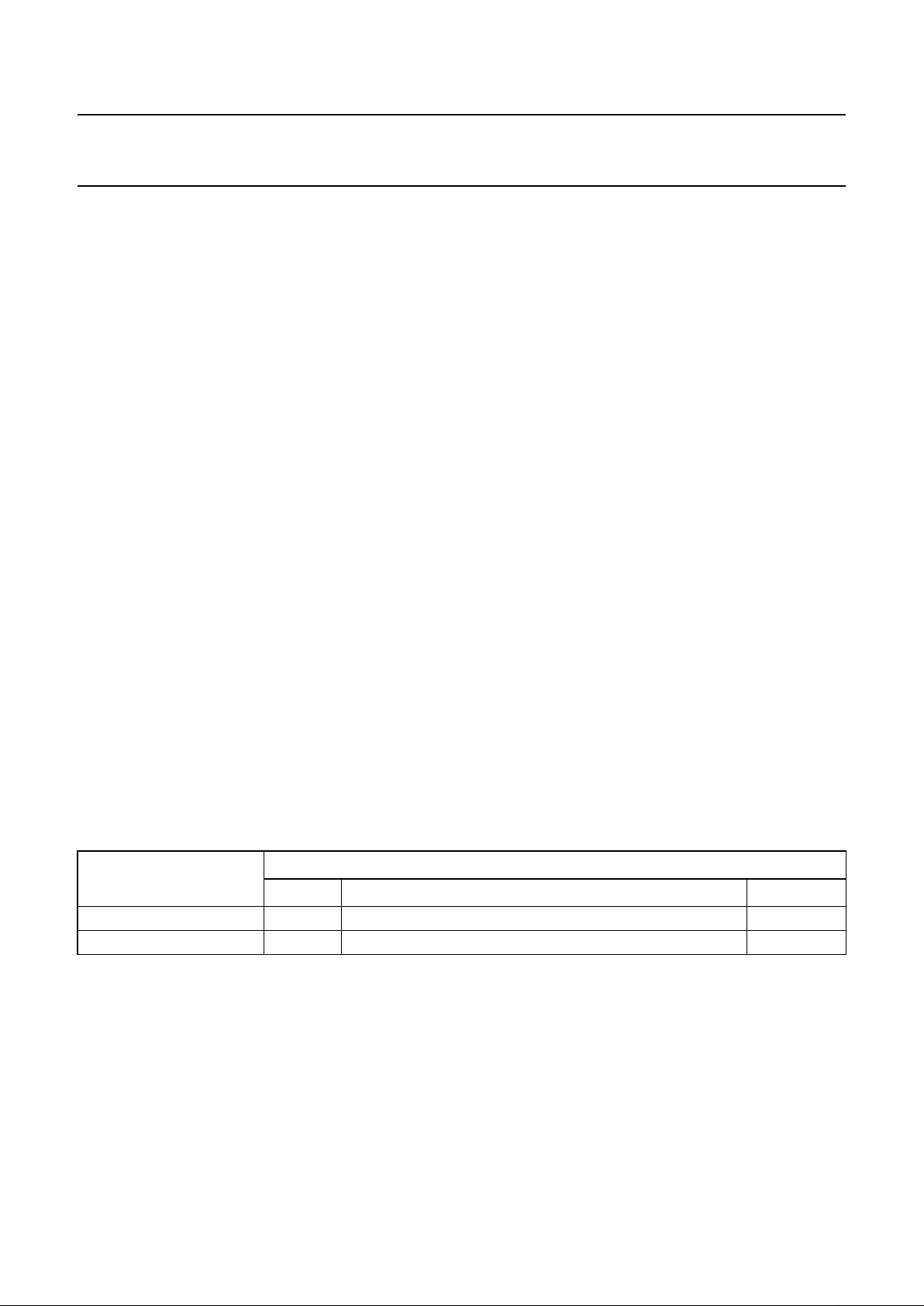
4 BLOCK DIAGRAM
handbook, full pagewidth
OSCILLATOR
MBG098
PORT 0
FLIP-FLOP
PORT 0
BUFFER
88
HIGHER
PROGRAM
COUNTER
LOWER
PROGRAM
COUNTER
PROGRAM
STATUS
WORD
MEMORY
BANK
FLIP-FLOPS
RESIDENT ROM
4 kbytes
DECODE
8
T1
8
8
5 888 8
8
P0.0 to P0.7
RAM
ADDRESS
REGISTER
ACCUMULATOR
TEMPORARY
REGISTER 1
PCD3349A
HGF
REGISTER
8
88
LGF
REGISTER
SINE WAVE
GENERATOR
TEMPORARY
REGISTER 2
ARITHMETIC
LOGIC UNIT
INSTRUCTION
REGISTER
&
DECODER
DECIMAL
ADJUST
CONTROL & TIMING
XTAL 2XTAL 1RESET
STOP
IDLE
INTERRUPT
INITIALIZE
CONDITIONAL
BRANCH
LOGIC
CE / T0
CE / T0
T1
TIMER
FLAG
CARRY
ACC
ACC BIT
TEST
RESIDENT RAM ARRAY
224 bytes
MULTIPLEXER
8 LEVEL STACK
(VARIABLE LENGTH)
OPTIONAL SECOND
REGISTER BANK
DATA STORE
D
E
C
O
D
E
REGISTER 0
REGISTER 1
REGISTER 2
REGISTER 3
REGISTER 4
REGISTER 5
REGISTER 6
REGISTER 7
PORT 1
FLIP-FLOP
PORT 1
BUFFER
P1.0 to P1.7
8
8
PORT 2
FLIP-FLOP
PORT 2
BUFFER
P2.0 to P2.3
4
4
TIMER/
EVENT
COUNTER
32
INTERNAL
CLOCK
FREQUENCY
30
8
88 8 8
INTERRUPT
LOGIC
timer interrupt
external interrupt
TONE
FILTER
POWER-ON-RESET
V
POR
RESET
Fig.1 Block diagram.
Page 5
1998 May 11 5
Philips Semiconductors Product specification
8-bit microcontroller with DTMF generator PCD3349A
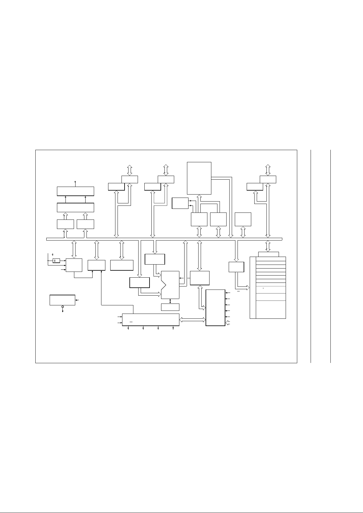
5 PINNING INFORMATION
5.1 Pinning
Fig.2 Pin configuration (SOT117-1 and SOT136-1).
handbook, halfpage
PCD3349A
MBG087
1
2
3
4
5
6
7
8
9
10
11
12
13
14
28
27
26
25
24
23
22
21
20
19
18
17
16
15
P0.1 P0.0
P2.3
P2.2
P2.1
V
DD
TONE
V
SS
P2.0
P1.7
P1.6
P1.5
P1.4
P1.3
P1.2
P0.2
P0.3
P0.4
P0.5
P0.6
P0.7
T1
XTAL1
XTAL2
RESET
P1.0
P1.1
CE/T0
5.2 Pin description
Table 1 SOT117-1 and SOT136-1 packages
SYMBOL PIN DESCRIPTION
P0.0 to P0.7 28, 1 to 7 Port 0: 8 quasi-bidirectional
I/O lines
T1 8 Test 1 or count input of 8-bit
Timer/event counter 1
XTAL1 9 crystal oscillator or external
clock input
XTAL2 10 crystal oscillator output
RESET 11 reset input
CE/
T0 12 Chip Enable or Test 0
P1.0 to P1.7 13 to 20 Port 1: 8 quasi-bidirectional
I/O lines
P2.0 to P2.3 21, 25,
26, 27
Port 2: 4 quasi-bidirectional
I/O lines
V
SS
22 ground
TONE 23 DTMF output
V
DD
24 positive supply voltage
Page 6
1998 May 11 6
Philips Semiconductors Product specification
8-bit microcontroller with DTMF generator PCD3349A
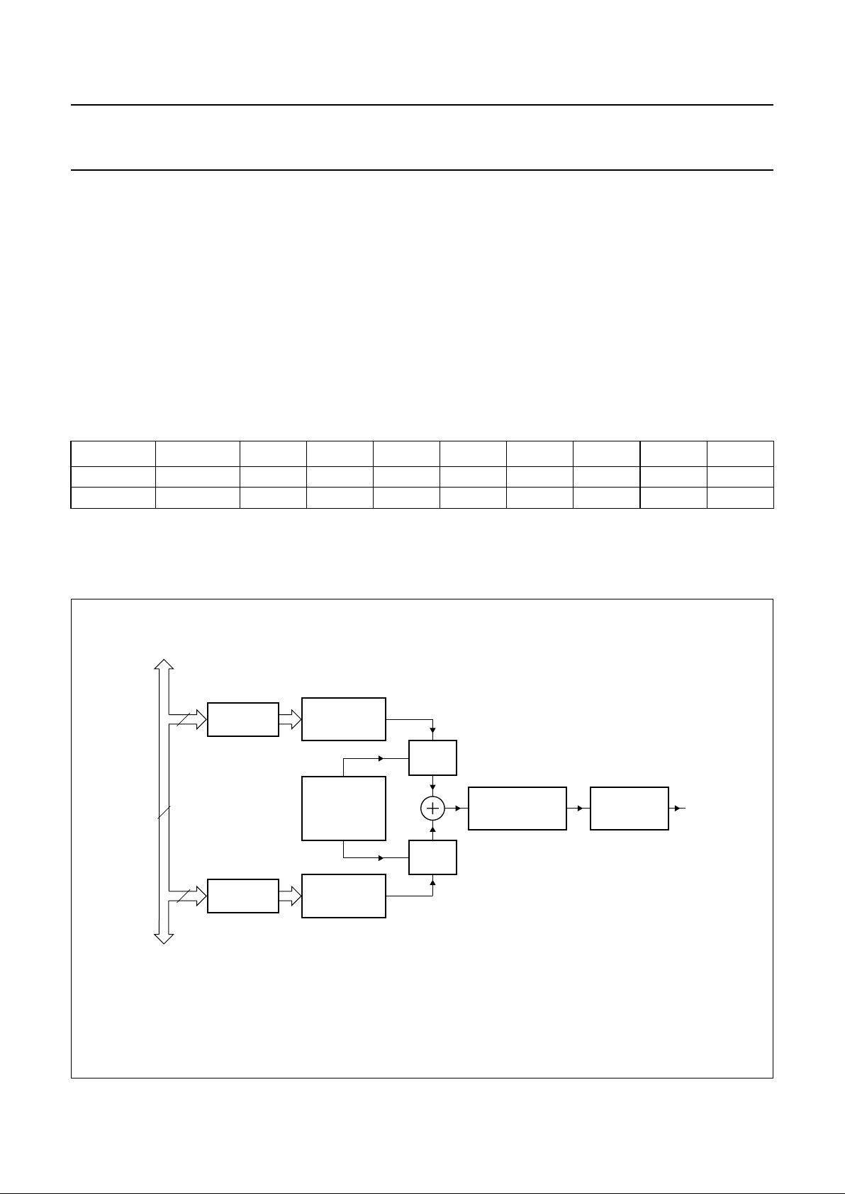
6 FREQUENCY GENERATOR
A versatile frequency generator section is provided (see
Fig.3). For normal operation, use a 3.58 MHz quartz
crystal or PXE resonator. The frequency generator
includes precision circuitry for dual tone multifrequency
(DTMF) signals, which is typically used for tone dialling
telephone sets.
The TONE output can alternatively issue twelve modem
frequencies for data rates between 300 and 1200 bits/s.
In addition to DTMF and modem frequencies, two octaves
of musical scale in steps of semitones are available.
6.1 Frequency generator derivative registers
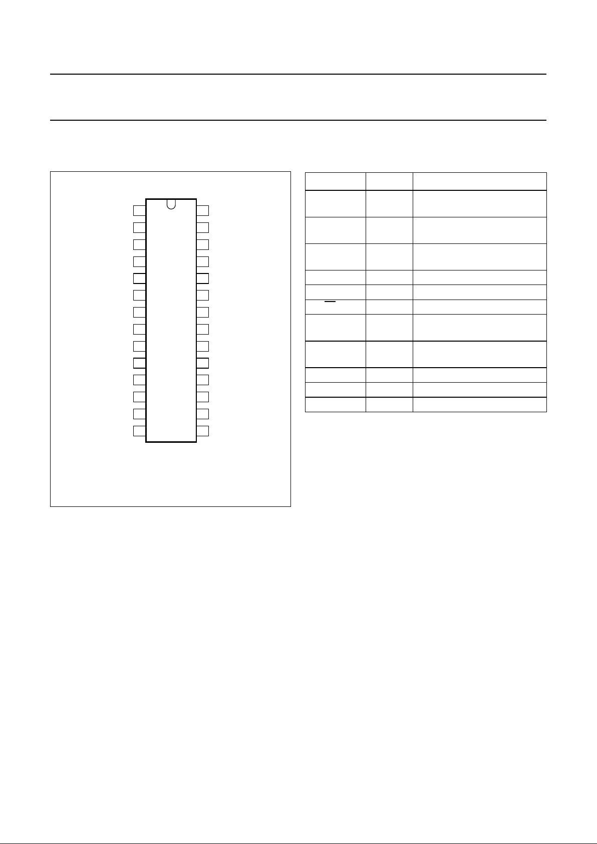
Table 2 gives the derivative addresses, mnemonics and access types of the frequency generator derivative registers.
The addresses 03H to FFH are not used.
Table 2 Addresses of the frequency generator derivative registers
Notes
1. HGF = High Group Frequency; access type W.
2. LGF = Low Group Frequency; access type W.
ADDRESS REGISTER 7 6 5 4 3 2 1 0
01H HGF
(1)
H7 H6 H5 H4 H3 H2 H1 H0
02H LGF
(2)
L7 L6 L5 L4 L3 L2 L1 L0
Fig.3 Block diagram of the frequency generator section.
book, full pagewidth
HGF
REGISTER
MBG099
DIGITAL
SINE WAVE
SYNTHESIZER
8
SWITCHED-
CAPACITOR
BANDGAP
VOLTAGE
REFERENCE
DAC
DAC
LGF
REGISTER
DIGITAL
SINE WAVE
SYNTHESIZER
8
8 internal bus
SWITCHED-
CAPACITOR
LOW-PASS FILTER
RC LOW-PASS
FILTER
TONE
Page 7

1998 May 11 7
Philips Semiconductors Product specification
8-bit microcontroller with DTMF generator PCD3349A
6.2 Frequency registers
The two frequency registers HGF and LGF define two
frequencies. From these, the digital sine synthesizers
together with the Digital-to-Analog Converters (DACs)
construct two sine waves. Their amplitudes are precisely
scaled according to the bandgap voltage reference. This
ensures TONE output levels independent of supply
voltage and temperature. The amplitude of the Low Group
Frequency sine wave is attenuated by 2 dB compared to
the amplitude of the High Group Frequency sine wave.
The two sine waves are summed and then filtered by an
on-chip switched capacitor and RC low-pass filters. These
guarantee that all DTMF tones generated fulfil the CEPT
recommendations with respect to amplitude, frequency
deviation, total harmonic distortion and suppression of
unwanted frequency components.
The value 00H in a frequency register stops the
corresponding digital sine synthesizer. If both frequency
registers contain 00H, the whole frequency generator is
shut off, resulting in lower power consumption.
The frequency of the sine wave generated is dependent
upon the decimal value ‘x’ held in the frequency registers
(HGF and LGF), and this may be calculated as follows:
; where 60 ≤ x ≤ 255.
The frequency limitation given by x ≥ 60 is due to the
low-pass filters which would attenuate higher frequency
sine waves.
6.3 DTMF frequencies
Assuming an oscillator frequency f
xtal
= 3.58 MHz, the
DTMF standard frequencies can be implemented as
shown in Table 3.
The relationship between telephone keyboard symbols
and the frequency register contents are given in Table 4.
f
f
xtal
23 x 2+()[]
--------------------------------
-
=
Table 3 DTMF standard frequencies and their
implementation; value = LGF, HGF contents
Table 4 Dialling symbols, corresponding DTMF
frequency pairs and frequency registers content
VALUE
(HEX)
FREQUENCY (Hz) DEVIATION
STANDARD GENERATED (%) (Hz)
DD 697 697.90 0.13 0.90
C8 770 770.46 0.06 0.46
B5 852 850.45 −0.18 −1.55
A3 941 943.23 0.24 2.23
7F 1209 1206.45 −0.21 −2.55
72 1336 1341.66 0.42 5.66
67 1477 1482.21 0.35 5.21
5D 1633 1638.24 0.32 5.24
TELEPHONE
KEYBOARD
SYMBOLS
DTMF FREQ.
PAIRS
(Hz)
LGF
VALUE
(HEX)
HGF
VALUE
(HEX)
0 (941, 1336) A3 72
1 (697, 1209) DD 7F
2 (697, 1336) DD 72
3 (697, 1477) DD 67
4 (770, 1209) C8 7F
5 (770, 1336) C8 72
6 (770, 1477) C8 67
7 (852, 1209) B5 7F
8 (852, 1336) B5 72
9 (852, 1477) B5 67
A (697, 1633) DD 5D
B (770, 1633) C8 5D
C (852, 1633) B5 5D
D (941, 1633) A3 5D
• (941, 1209) A3 7F
# (941, 1477) A3 67
Page 8

1998 May 11 8
Philips Semiconductors Product specification
8-bit microcontroller with DTMF generator PCD3349A
6.4 Modem frequencies
Again assuming an oscillator frequency f
xtal
= 3.58 MHz,
the standard modem frequency pairs summarized in
Table 5 can be implemented. It is suggested to define the
frequency by the HGF register while the LGF register
contains 00H, disabling Low Group Frequency generation.
Table 5 Standard modem frequency pairs and their
implementation
Notes
1. Standard is V.21.
2. Standard is Bell 103.
3. Standard is Bell 202.
4. Standard is V.23.
6.5 Musical scale frequencies
Finally, two octaves of musical scale in steps of semitones
can be realized, again assuming an oscillator frequency
f
xtal
= 3.58 MHz (Table 6). It is suggested to define the
frequency by the HGF register while the LGF contains
00H, disabling Low Group Frequency generation.
HGF
VALU
E
(HEX)
FREQUENCY (Hz) DEVIATION
MODEM GENERATED (%) (Hz)
9D 980
(1)
978.82 −0.12 −1.18
82 1180
(1)
1179.03 −0.08 −0.97
8F 1070
(2)
1073.33 0.31 3.33
79 1270
(2)
1265.30 −0.37 −4.70
80 1200
(3)
1197.17 −0.24 −2.83
45 2200
(3)
2192.01 −0.36 −7.99
76 1300
(4)
1296.94 −0.24 −3.06
48 2100
(4)
2103.14 0.15 3.14
5C 1650
(1)
1655.66 0.34 5.66
52 1850
(1)
1852.77 0.15 2.77
4B 2025
(2)
2021.20 −0.19 −3.80
44 2225
(2)
2223.32 −0.08 −1.68
Table 6 Musical scale frequencies and their
implementation
Note
1. Standard scale based on A4 at 440 Hz.
NOTE
HGF
VALUE
(HEX)
FREQUENCY (Hz)
STANDARD
(1)
GENERATED
D#5 F8 622.3 622.5
E5 EA 659.3 659.5
F5 DD 698.5 697.9
F#5 D0 740.0 741.1
G5 C5 784.0 782.1
G#5 B9 830.6 832.3
A5 AF 880.0 879.3
A#5 A5 923.3 931.9
B5 9C 987.8 985.0
C6 93 1046.5 1044.5
C#6 8A 1108.7 1111.7
D6 82 1174.7 1179.0
D#6 7B 1244.5 1245.1
E6 74 1318.5 1318.9
F6 6D 1396.9 1402.1
F#6 67 1480.0 1482.2
G6 61 1568.0 1572.0
G#6 5C 1661.2 1655.7
A6 56 1760.0 1768.5
A#6 51 1864.7 1875.1
B6 4D 1975.5 1970.0
C7 48 2093.0 2103.3
C#7 44 2217.5 2223.3
D7 40 2349.3 2358.1
D#7 3D 2489.0 2470.4
Page 9

1998 May 11 9
Philips Semiconductors Product specification
8-bit microcontroller with DTMF generator PCD3349A
7 TIMING
Although the PCD3349A operates over a clock frequency
range from 1 to 16 MHz, f
xtal
= 3.58 MHz will usually be
chosen to take full advantage of the frequency generator
section.
8 RESET
In addition to the conditions given in the
“PCD33xxA
Family”
data sheet, all derivative registers are cleared in
the RESET state.
9 STOP MODE
Since the oscillator is switched off, the frequency
generator receives no clock. It is suggested to clear both
the HGF and LGF registers before entering Stop mode.
This will cut-off the biasing of the internal amplifiers,
considerably reducing current requirements.
10 IDLE MODE
In the Idle mode, the frequency generator remains
operative.
11 INSTRUCTION SET RESTRICTIONS
Since no serial I/O interface is provided, the serial I/O
(Input/Output) instructions are not available. ‘MOV Dx, A’
is the only applicable derivative instruction because the
derivative registers are write-only.
ROM space being restricted to 4 kbytes, SEL MB2/3 would
define non-existing Program Memory banks and should
therefore be avoided.
RAM space being restricted to 224 bytes, care should be
taken to avoid accesses to non-existing RAM locations.
12 SUMMARY OF MASK OPTIONS
Table 7 Port mask options
Notes
1. Port output drives:
a) Option 1: standard I/O.
b) Option 2: open-drain I/O.
c) Option 3: push-pull output; see
“PCD33xxA Family”
data sheet.
2. Port state after reset: S = Set (HIGH) and R = Reset (LOW).
Table 8 Mask options
PORT NAME
PORT OUTPUT DRIVE
(1)
PORT STATE AFTER RESET
(2)
OPTION 1 OPTION 2 OPTION 3
SET RESET
Port 0 (P0.0 to P0.7) X X X X X
Port 1 (P1.0 to P1.7) X X X X X
Port 2 (P2.0 to P2.7) X X X X X
FEATURE DESCRIPTION
ROM code: program/data Any mix of instructions and data up to ROM size of 4 kbytes.
Power-on-reset voltage level: V
POR
1.2 to 3.6 V in increments of 100 mV; OFF
Oscillator transconductance: g
m
LOW transconductance: g
mL
MEDIUM transconductance: g
mM
HIGH transconductance: g
mH
Page 10

1998 May 11 10
Philips Semiconductors Product specification
8-bit microcontroller with DTMF generator PCD3349A
13 LIMITING VALUES
In accordance with the Absolute Maximum Rating System (IEC 134); see note 1 and 2.
Notes
1. Stresses above those listed under Limiting Values may cause permanent damage to the device.
2. Parameters are valid over operating temperature range unless otherwise specified. All voltages are with respect to
V
SS
unless otherwise noted.
14 HANDLING
Inputs and outputs are protected against electrostatic discharge in normal handling. However, it is good practice to take
normal precautions appropriate to handling MOS devices (see
“Handling MOS devices”
).
15 DC CHARACTERISTICS
V
DD
= 1.8 to 6 V; VSS=0V; T
amb
= −25 to +70 °C; all voltages with respect to VSS; f
xtal
= 3.58 MHz (gmL); unless
otherwise specified.
SYMBOL PARAMETER MIN. MAX. UNIT
V
DD
supply voltage −0.5 +7.0 V
V
I
all input voltages −0.5 VDD+ 0.5 V
I
I,IO
DC input or output current −10 +10 mA
P
tot
total power dissipation − 125 mW
P
O
power dissipation per output − 30 mW
I
SS
ground supply current −50 +50 mA
T
stg
storage temperature −65 +150 °C
T
j
operating junction temperature − 90 °C
SYMBOL PARAMETER CONDITIONS MIN. TYP. MAX. UNIT
Supply (see Figs 5 to 9)
V
DD
supply voltage
operating; note 1 1.8 − 6V
RAM data retention in
Stop mode
1.0 − 6V
I
DD
operating supply current;
note 2
VDD= 3 V; value HGF ≠ 0 and/or LGF ≠ 0 − 0.9 1.8 mA
V
DD
=3V − 0.3 0.6 mA
V
DD
=5V; f
xtal
= 10 MHz (gmL) − 1.1 3.0 mA
V
DD
=5V; f
xtal
= 16 MHz (gmM) − 1.7 5.0 mA
V
DD
=5V; f
xtal
= 16 MHz (gmH) − 2.5 6.0 mA
I
DD(idle)
supply current Idle mode;
note 2
VDD= 3 V; value HGF ≠ 0 and/or LGF ≠ 0 − 0.7 1.4 mA
V
DD
= 3 V; value HGF = LGF = 0 − 0.2 0.4 mA
V
DD
=5V; f
xtal
= 10 MHz (gmL) − 0.8 1.6 mA
V
DD
=5V; f
xtal
= 16 MHz (gmM) − 1.2 4.0 mA
V
DD
=5V; f
xtal
= 16 MHz (gmH) − 1.7 5.0 mA
I
DD(stp)
supply current Stop mode VDD= 1.8 V; T
amb
=25°C; note 3 − 1.0 2.5 µA
V
DD
= 1.8 V; T
amb
=70°C; note 3 −−10 µA
Page 11

1998 May 11 11
Philips Semiconductors Product specification
8-bit microcontroller with DTMF generator PCD3349A
Notes
1. TONE output requires VDD≥ 2.5 V.
2. VIL=VSS; VIH=VDD; open-drain outputs connected to VSS; all other outputs open; value HGF = LGF = 0, unless
otherwise specified.
3. Crystal connected between XTAL1 and XTAL2; pins T1 and CE/T0 at VSS; value HGF = LGF = 0.
4. Values are specified for DTMF frequencies only (CEPT).
5. Related to the Low Group Frequency (LGF) component (CEPT).
6. V
POR
is an option chosen by the user. Depending on its value, it may restrict the supply voltage range.
Inputs
V
IL
LOW-level input voltage 0 − 0.3VDDV
V
IH
HIGH-level input voltage 0.7VDD− V
DD
V
I
IL
input leakage current VSS≤ VI≤ V
DD
−1 − +1 µA
Port outputs (see Figs 10 to 12)
I
OL
LOW-level port sink
current
VDD= 3 V; VO= 0.4 V 0.7 3.5 − mA
I
OH
HIGH-level port pull-up
source current
VO= 2.7 V; VDD=3V −10 −20 −µA
V
O
=0V; VDD=3V −−100 −300 µA
I
OH
HIGH-level port push-pull
source current
VDD= 3 V; VO= 2.6 V −0.7 −4 − mA
TONE output (see Fig.4; notes 1 and 4)
V
HGrms
HGF voltage (RMS) 158 181 205 mV
V
LGrms
LGF voltage (RMS) 125 142 160 mV
frequency deviation −0.6 − 0.6 %
V
DC
DC voltage level − 0.5VDD− V
Z
O
output impedance − 100 500 Ω
V
G
pre-emphasis of group 1.5 2.0 2.5 dB
THD total harmonic distortion T
amb
=25°C; note 5 − 25 − dB
Power-on-reset
∆V
POR
Power-on-reset level
variation around chosen
V
POR
note 6 −0.5 0 +0.5 V
SYMBOL PARAMETER CONDITIONS MIN. TYP. MAX. UNIT
f∆ f⁄
Page 12

1998 May 11 12
Philips Semiconductors Product specification
8-bit microcontroller with DTMF generator PCD3349A
Fig.4 TONE output test circuit.
handbook, halfpage
MGB835
10 kΩ
TONE
50 pF
1 µF
DEVICE TYPE NUMBER
(1)
V
DD
V
SS
(1) Device type number: PCD3349A
Fig.5 Typical supply current (IDD) in Stop mode as
a function of supply voltage (VDD).
handbook, halfpage
1
6
4
3
1
5
2
0
35
V
DD
(V)
7
MGB826
I
DD(stp)
(µA)
Fig.6 Typical operating supply current (IDD) as a
function of supply voltage (VDD).
andbook, halfpage
1
6
4
2
0
35
V
DD
(V)
7
MGB827
I
DD
(mA)
16 MHz
3.58 MHz
HGF or LGF ≠ 0
10 MHz
3.58 MHz
Measured with crystal between XTAL1 and XTAL2.
Fig.7 Typical operating supply current (IDD) as a
function of clock frequency (f
xtal
).
handbook, halfpage
6
0
2
2
4
1
MGB828
10 10
I
DD
(mA)
f
xtal
(MHz)
3 V
5 V
Measured with function generator on XTAL1.
Page 13

1998 May 11 13
Philips Semiconductors Product specification
8-bit microcontroller with DTMF generator PCD3349A
Fig.8 Typical supply current (IDD) in Idle mode as
a function of supply voltage (VDD).
andbook, halfpage
1
6
4
2
0
35
V
DD
(V)
7
MGB829
I
DD(idle)
(mA)
16 MHz
3.58 MHz
HGF or LGF ≠ 0
10 MHz
3.58 MHz
Measured with crystal between XTAL1 and XTAL2.
Fig.9 Typical supply current (IDD) in Idle mode as
a function of clock frequency (f
xtal
).
Measured with function generator on XTAL1.
handbook, halfpage
6
0
2
2
4
1
MGB830
10 10
I
DD(idle)
(mA)
f
xtal
(MHz)
3 V
5 V
Fig.10 Typical LOW-level port output sink current
(IOL) as a function of supply voltage (VDD).
VO= 0.4 V.
handbook, halfpage
1
12
8
4
0
35
V
DD
(V)
7
MGB831
I
OL
(mA)
Fig.11 Typical HIGH-level output pull-up source
current (IOH) as a function of supply voltage
(VDD).
handbook, halfpage
MBG095
VDD(V)
135 7
−200
−100
0
−300
(µA)
I
OH
SS
V = V
O
DD
V = 0.9V
O
Page 14

1998 May 11 14
Philips Semiconductors Product specification
8-bit microcontroller with DTMF generator PCD3349A
Fig.12 Typical HIGH-level push-pull output source
current (IOH) as a function of supply voltage
(VDD).
VO=VDD− 0.4 V.
handbook, halfpage
1
−12
−8
−4
0
35
V
DD
(V)
7
MGB833
I
OH1
(mA)
Fig.13 Typical Power-on-reset level (V
POR
) as
function of temperature.
handbook, halfpage
−25
6
4
2
0
25 75
70
T
amb
(°C)
125
MGD495
V
DD
(V)
V
POR
= 1.3 V
V
POR
= 2.0 V
Page 15

1998 May 11 15
Philips Semiconductors Product specification
8-bit microcontroller with DTMF generator PCD3349A
16 AC CHARACTERISTICS
V
DD
= 1.8 to 6 V; VSS=0V; T
amb
= −25 to +70 °C; all voltages with respect to VSS; unless otherwise specified.
SYMBOL PARAMETER CONDITIONS MIN. TYP. MAX. UNIT
t
r
rise time all outputs VDD=5V; T
amb
=25°C; CL=50pF − 30 − ns
t
f
fall time all outputs − 30 − ns
f
xtal
clock frequency see Fig.14 1 − 16 MHz
Oscillator (see Fig.15)
g
mL
LOW transconductance VDD= 5 V 0.2 0.4 1.0 mS
g
mM
MEDIUM transconductance 0.9 1.6 3.2 mS
g
mH
HIGH transconductance 3.0 4.5 9.0 mS
R
F
feedback resistor 0.3 1.0 3.0 MΩ
handbook, halfpage
MLA493
VDD (V)
135 7
f
xtal
(MHz)
12
9
6
3
0
15
18
guaranteed
operating range
Fig.14 Maximum clock frequency (f
xtal
) as a
function of supply voltage (VDD).
Fig.15 Typical transconductance as a function of
supply voltage (VDD).
handbook, halfpage
1357
V
DD
(V)
10
−1
MBG097
1
10
g
m
(mS)
g
mH
g
mM
g
mL
Page 16

1998 May 11 16
Philips Semiconductors Product specification
8-bit microcontroller with DTMF generator PCD3349A
17 PACKAGE OUTLINES
UNIT
A
max.
1 2
b
1
(1)
(1) (1)
cD E weM
H
L
REFERENCES
OUTLINE
VERSION
EUROPEAN
PROJECTION
ISSUE DATE
IEC JEDEC EIAJ
mm
inches
DIMENSIONS (inch dimensions are derived from the original mm dimensions)
SOT117-1
92-11-17
95-01-14
A
min.
A
max.
b
Z
max.
M
E
e
1
1.7
1.3
0.53
0.38
0.32
0.23
36.0
35.0
14.1
13.7
3.9
3.4
0.252.54 15.24
15.80
15.24
17.15
15.90
1.75.1 0.51 4.0
0.066
0.051
0.020
0.014
0.013
0.009
1.41
1.34
0.56
0.54
0.15
0.13
0.010.10 0.60
0.62
0.60
0.68
0.63
0.0670.20 0.020 0.16
051G05 MO-015AH
M
H
c
(e )
1
M
E
A
L
seating plane
A
1
w M
b
1
e
D
A
2
Z
28
1
15
14
b
E
pin 1 index
0 5 10 mm
scale
Note
1. Plastic or metal protrusions of 0.25 mm maximum per side are not included.
handbook, full pagewidth
DIP28: plastic dual in-line package; 28 leads (600 mil)
SOT117-1
Page 17

1998 May 11 17
Philips Semiconductors Product specification
8-bit microcontroller with DTMF generator PCD3349A
UNIT
A
max.
A
1
A2A3b
p
cD
(1)E(1) (1)
eHELLpQ
Z
ywv θ
REFERENCES
OUTLINE
VERSION
EUROPEAN
PROJECTION
ISSUE DATE
IEC JEDEC EIAJ
mm
inches
2.65
0.30
0.10
2.45
2.25
0.49
0.36
0.32
0.23
18.1
17.7
7.6
7.4
1.27
10.65
10.00
1.1
1.0
0.9
0.4
8
0
o
o
0.25 0.1
DIMENSIONS (inch dimensions are derived from the original mm dimensions)
Note
1. Plastic or metal protrusions of 0.15 mm maximum per side are not included.
1.1
0.4
SOT136-1
X
14
28
w M
θ
A
A
1
A
2
b
p
D
H
E
L
p
Q
detail X
E
Z
c
L
v M
A
e
15
1
(A )
3
A
y
0.25
075E06 MS-013AE
pin 1 index
0.10
0.012
0.004
0.096
0.089
0.019
0.014
0.013
0.009
0.71
0.69
0.30
0.29
0.050
1.4
0.055
0.419
0.394
0.043
0.039
0.035
0.016
0.01
0.25
0.01
0.004
0.043
0.016
0.01
0 5 10 mm
scale
SO28: plastic small outline package; 28 leads; body width 7.5 mm
SOT136-1
95-01-24
97-05-22
Page 18

1998 May 11 18
Philips Semiconductors Product specification
8-bit microcontroller with DTMF generator PCD3349A
18 SOLDERING
18.1 Introduction
There is no soldering method that is ideal for all IC
packages. Wave soldering is often preferred when
through-hole and surface mounted components are mixed
on one printed-circuit board. However, wave soldering is
not always suitable for surface mounted ICs, or for
printed-circuits with high population densities. In these
situations reflow soldering is often used.
This text gives a very brief insight to a complex technology.
A more in-depth account of soldering ICs can be found in
our
“Data Handbook IC26; Integrated Circuit Packages”
(order code 9398 652 90011).
18.2 DIP
18.2.1 S
OLDERING BY DIPPING OR BY WAVE
The maximum permissible temperature of the solder is
260 °C; solder at this temperature must not be in contact
with the joint for more than 5 seconds. The total contact
time of successive solder waves must not exceed
5 seconds.
The device may be mounted up to the seating plane, but
the temperature of the plastic body must not exceed the
specified maximum storage temperature (T
stg max
). If the
printed-circuit board has been pre-heated, forced cooling
may be necessary immediately after soldering to keep the
temperature within the permissible limit.
18.2.2 R
EPAIRING SOLDERED JOINTS
Apply a low voltage soldering iron (less than 24 V) to the
lead(s) of the package, below the seating plane or not
more than 2 mm above it. If the temperature of the
soldering iron bit is less than 300 °C it may remain in
contact for up to 10 seconds. If the bit temperature is
between 300 and 400 °C, contact may be up to 5 seconds.
18.3 SO
18.3.1 REFLOW SOLDERING
Reflow soldering techniques are suitable for all SO
packages.
Reflow soldering requires solder paste (a suspension of
fine solder particles, flux and binding agent) to be applied
to the printed-circuit board by screen printing, stencilling or
pressure-syringe dispensing before package placement.
Several techniques exist for reflowing; for example,
thermal conduction by heated belt. Dwell times vary
between 50 and 300 seconds depending on heating
method. Typical reflow temperatures range from
215 to 250 °C.
Preheating is necessary to dry the paste and evaporate
the binding agent. Preheating duration: 45 minutes at
45 °C.
18.3.2 W
AVE SOLDERING
Wave soldering techniques can be used for all SO
packages if the following conditions are observed:
• A double-wave (a turbulent wave with high upward
pressure followed by a smooth laminar wave) soldering
technique should be used.
• The longitudinal axis of the package footprint must be
parallel to the solder flow.
• The package footprint must incorporate solder thieves at
the downstream end.
During placement and before soldering, the package must
be fixed with a droplet of adhesive. The adhesive can be
applied by screen printing, pin transfer or syringe
dispensing. The package can be soldered after the
adhesive is cured.
Maximum permissible solder temperature is 260 °C, and
maximum duration of package immersion in solder is
10 seconds, if cooled to less than 150 °C within
6 seconds. Typical dwell time is 4 seconds at 250 °C.
A mildly-activated flux will eliminate the need for removal
of corrosive residues in most applications.
18.3.3 R
EPAIRING SOLDERED JOINTS
Fix the component by first soldering two diagonallyopposite end leads. Use only a low voltage soldering iron
(less than 24 V) applied to the flat part of the lead. Contact
time must be limited to 10 seconds at up to 300 °C. When
using a dedicated tool, all other leads can be soldered in
one operation within 2 to 5 seconds between
270 and 320 °C.
Page 19

1998 May 11 19
Philips Semiconductors Product specification
8-bit microcontroller with DTMF generator PCD3349A
19 DEFINITIONS
20 LIFE SUPPORT APPLICATIONS
These products are not designed for use in life support appliances, devices, or systems where malfunction of these
products can reasonably be expected to result in personal injury. Philips customers using or selling these products for
use in such applications do so at their own risk and agree to fully indemnify Philips for any damages resulting from such
improper use or sale.
Data sheet status
Objective specification This data sheet contains target or goal specifications for product development.
Preliminary specification This data sheet contains preliminary data; supplementary data may be published later.
Product specification This data sheet contains final product specifications.
Limiting values
Limiting values given are in accordance with the Absolute Maximum Rating System (IEC 134). Stress above one or
more of the limiting values may cause permanent damage to the device. These are stress ratings only and operation
of the device at these or at any other conditions above those given in the Characteristics sections of the specification
is not implied. Exposure to limiting values for extended periods may affect device reliability.
Application information
Where application information is given, it is advisory and does not form part of the specification.
Page 20

Internet: http://www.semiconductors.philips.com
Philips Semiconductors – a worldwide company
© Philips Electronics N.V. 1998 SCA60
All rights are reserved. Reproduction in whole or in part is prohibited without the prior written consent of the copyright owner.
The information presented in this document does not form part of any quotation or contract, is believed to be accurate and reliable and may be changed
without notice. No liability will be accepted by the publisher for any consequence of its use. Publication thereof does not convey nor imply any license
under patent- or other industrial or intellectual property rights.
Middle East: see Italy
Netherlands: Postbus 90050, 5600 PB EINDHOVEN, Bldg. VB,
Tel. +31 40 27 82785, Fax. +31 40 27 88399
New Zealand: 2 Wagener Place, C.P.O. Box 1041, AUCKLAND,
Tel. +64 9 849 4160, Fax. +64 9 849 7811
Norway: Box 1, Manglerud 0612, OSLO,
Tel. +47 22 74 8000, Fax. +47 22 74 8341
Pakistan: see Singapore
Philippines: Philips Semiconductors Philippines Inc.,
106 Valero St. Salcedo Village, P.O. Box 2108 MCC, MAKATI,
Metro MANILA, Tel. +63 2 816 6380, Fax. +63 2 817 3474
Poland: Ul. Lukiska 10, PL 04-123 WARSZAWA,
Tel. +48 22 612 2831, Fax. +48 22 612 2327
Portugal: see Spain
Romania: see Italy
Russia: Philips Russia, Ul. Usatcheva 35A, 119048 MOSCOW,
Tel. +7 095 755 6918, Fax. +7 095 755 6919
Singapore: Lorong 1, Toa Payoh, SINGAPORE 319762,
Tel. +65 350 2538, Fax. +65 251 6500
Slovakia: see Austria
Slovenia: see Italy
South Africa: S.A. PHILIPS Pty Ltd., 195-215 Main Road Martindale,
2092 JOHANNESBURG, P.O. Box 7430 Johannesburg 2000,
Tel. +27 11 470 5911, Fax. +27 11 470 5494
South America: Al. Vicente Pinzon, 173, 6th floor,
04547-130 SÃO PAULO, SP, Brazil,
Tel. +55 11 821 2333, Fax. +55 11 821 2382
Spain: Balmes 22, 08007 BARCELONA,
Tel. +34 93 301 6312, Fax. +34 93 301 4107
Sweden: Kottbygatan 7, Akalla, S-16485 STOCKHOLM,
Tel. +46 8 5985 2000, Fax. +46 8 5985 2745
Switzerland: Allmendstrasse 140, CH-8027 ZÜRICH,
Tel. +41 1 488 2741 Fax. +41 1 488 3263
Taiwan: Philips Semiconductors, 6F, No. 96, Chien Kuo N. Rd., Sec. 1,
TAIPEI, Taiwan Tel. +886 2 2134 2865, Fax. +886 2 2134 2874
Thailand: PHILIPS ELECTRONICS (THAILAND) Ltd.,
209/2 Sanpavuth-Bangna Road Prakanong, BANGKOK 10260,
Tel. +66 2 745 4090, Fax. +66 2 398 0793
Turkey: Talatpasa Cad. No. 5, 80640 GÜLTEPE/ISTANBUL,
Tel. +90 212 279 2770, Fax. +90 212 282 6707
Ukraine: PHILIPS UKRAINE, 4 Patrice Lumumba str., Building B, Floor 7,
252042 KIEV, Tel. +380 44 264 2776, Fax. +380 44 268 0461
United Kingdom: Philips Semiconductors Ltd., 276 Bath Road, Hayes,
MIDDLESEX UB3 5BX, Tel. +44 181 730 5000, Fax. +44 181 754 8421
United States: 811 East Arques Avenue, SUNNYVALE, CA 94088-3409,
Tel. +1 800 234 7381
Uruguay: see South America
Vietnam: see Singapore
Yugoslavia: PHILIPS, Trg N. Pasica 5/v, 11000 BEOGRAD,
Tel. +381 11 625 344, Fax.+381 11 635 777
For all other countries apply to: Philips Semiconductors,
International Marketing & Sales Communications, Building BE-p, P.O. Box 218,
5600 MD EINDHOVEN, The Netherlands, Fax. +31 40 27 24825
Argentina: see South America
Australia: 34 Waterloo Road, NORTH RYDE, NSW 2113,
Tel. +61 2 9805 4455, Fax. +61 2 9805 4466
Austria: Computerstr. 6, A-1101 WIEN, P.O. Box 213, Tel. +43 160 1010,
Fax. +43 160 101 1210
Belarus: Hotel Minsk Business Center, Bld. 3, r. 1211, Volodarski Str. 6,
220050 MINSK, Tel. +375 172 200 733, Fax. +375 172 200 773
Belgium: see The Netherlands
Brazil: seeSouth America
Bulgaria: Philips Bulgaria Ltd., Energoproject, 15thfloor,
51 James Bourchier Blvd., 1407 SOFIA,
Tel. +359 2 689 211, Fax. +359 2 689 102
Canada: PHILIPS SEMICONDUCTORS/COMPONENTS,
Tel. +1 800 234 7381
China/Hong Kong: 501 Hong Kong Industrial Technology Centre,
72 Tat Chee Avenue, Kowloon Tong, HONG KONG,
Tel. +852 2319 7888, Fax. +852 2319 7700
Colombia: see South America
Czech Republic: see Austria
Denmark: Prags Boulevard 80, PB 1919, DK-2300 COPENHAGEN S,
Tel. +45 32 88 2636, Fax. +45 31 57 0044
Finland: Sinikalliontie 3, FIN-02630 ESPOO,
Tel. +358 9 615800, Fax. +358 9 61580920
France: 51 Rue Carnot, BP317, 92156 SURESNES Cedex,
Tel. +33 1 40 99 6161, Fax. +33 1 40 99 6427
Germany: Hammerbrookstraße 69, D-20097 HAMBURG,
Tel. +49 40 23 53 60, Fax. +49 40 23 536 300
Greece: No. 15, 25th March Street, GR 17778 TAVROS/ATHENS,
Tel. +30 1 4894 339/239, Fax. +30 1 4814 240
Hungary: seeAustria
India: Philips INDIA Ltd, Band Box Building, 2nd floor,
254-D, Dr. Annie Besant Road, Worli, MUMBAI 400 025,
Tel. +91 22 493 8541, Fax. +91 22 493 0966
Indonesia: PT Philips Development Corporation, Semiconductors Division,
Gedung Philips, Jl. Buncit Raya Kav.99-100, JAKARTA 12510,
Tel. +62 21 794 0040 ext. 2501, Fax. +62 21 794 0080
Ireland: Newstead, Clonskeagh, DUBLIN 14,
Tel. +353 1 7640 000, Fax. +353 1 7640 200
Israel: RAPAC Electronics, 7 Kehilat Saloniki St, PO Box 18053,
TEL AVIV 61180, Tel. +972 3 645 0444, Fax. +972 3 649 1007
Italy: PHILIPS SEMICONDUCTORS, Piazza IV Novembre 3,
20124 MILANO, Tel. +39 2 6752 2531, Fax. +39 2 6752 2557
Japan: Philips Bldg 13-37, Kohnan 2-chome, Minato-ku,
TOKYO 108-8507, Tel. +81 3 3740 5130, Fax. +81 3 3740 5077
Korea: Philips House, 260-199 Itaewon-dong, Yongsan-ku, SEOUL,
Tel. +82 2 709 1412, Fax. +82 2 709 1415
Malaysia: No. 76 Jalan Universiti, 46200 PETALING JAYA, SELANGOR,
Tel. +60 3 750 5214, Fax. +60 3 757 4880
Mexico: 5900 Gateway East, Suite 200, EL PASO, TEXAS 79905,
Tel. +9-5 800 234 7381
Printed in The Netherlands 415102/1200/05/pp20 Date of release: 1998 May 11 Document order number: 9397 750 03605
 Loading...