

Page 1

INTEGRATED CIRCUITS
DATA SH EET
PCD3311C; PCD3312C
DTMF/modem/musical-tone
generators
Product specification
Supersedes data of May 1990
File under Integrated Circuits, IC03
1996 Nov 21
Page 2

Philips Semiconductors Product specification
DTMF/modem/musical-tone generators PCD3311C; PCD3312C
CONTENTS
1 FEATURES
2 GENERAL DESCRIPTION
3 QUICK REFERENCE DATA
4 ORDERING INFORMATION
5 BLOCK DIAGRAM
6 PINNING INFORMATION
6.1 Pinning PCD3311CP
6.2 Pin description PCD3311CP
6.3 Pinning PCD3311CT
6.4 Pin description PCD3311CT
6.5 Pinning PCD3312C
6.6 Pin description PCD3312C
7 FUNCTIONAL DESCRIPTION
7.1 General
7.2 Clock/oscillator connection
7.3 Mode selection (PCD3311C)
7.4 Data inputs (PCD3311C)
7.5 Strobe input (PCD3311C )
7.6 I2C-bus clock and data inputs
7.7 Address input
7.8 I2C-bus data configuration
7.9 Tone output
7.10 Power-on reset
7.11 Tables of Input and output
8I
8.1 Bit transfer
8.2 Start and stop conditions
8.3 System configuration
8.4 Acknowledge
8.5 Timing specifications
8.5.1 Standard mode
8.5.2 Low-speed mode
9 HANDLING
10 LIMITING VALUES
11 CHARACTERISTICS
12 APPLICATION INFORMATION
13 PACKAGE OUTLINES
14 SOLDERING
14.1 Introduction
14.2 DIP
14.2.1 Soldering by dipping or by wave
14.2.2 Repairing soldered joints
14.3 SO
14.3.1 Reflow soldering
14.3.2 Wave soldering
14.3.3 Repairing soldered joints
2
C-BUS INTERFACE
15 DEFINITIONS
16 LIFE SUPPORT APPLICATIONS
17 PURCHASE OF PHILIPS I2C COMPONENTS
1996 Nov 21 2
Page 3
Philips Semiconductors Product specification
DTMF/modem/musical-tone generators PCD3311C; PCD3312C
1 FEATURES
• DTMF, modem and musical tone generation
• Stabilized output voltage level
• Low output distortion with on-chip filtering conforming to
CEPT recommendations
• Latched inputs for data bus applications
• I2C-bus compatible
• Selection of parallel or serial (I2C-bus) data input
(PCD3311C).
used, and a separate microcontroller is required to control
the devices.
Both the devices can interface to I
2
C-bus compatible
microcontrollers for serial input. The PCD3311C can also
interface directly to all standard microcontrollers,
accepting a binary coded parallel input.
With their on-chip voltage reference the PCD3311C and
PCD3312C provide constant output amplitudes which are
independent of the operating supply voltage and ambient
temperature.
An on-chip filtering system assures a very low total
2 GENERAL DESCRIPTION
The PCD3311C and PCD3312C are single-chip silicon
gate CMOS integrated circuits. They are intended
principally for use in telephone sets to provide the
dual-tone multi-frequency (DTMF) combinations required
for tone dialling systems. The various audio output
frequencies are generated from an on-chip 3.58 MHz
quartz crystal-controlled oscillator. A separate crystal is
harmonic distortion in accordance with CEPT
recommendations.
In addition to the standard DTMF frequencies the devices
can also provide:
• Twelve standard frequencies used in simplex modem
applications for data rates from 300 to 1200 bits per
second
• Two octaves of musical scales in steps of semitones.
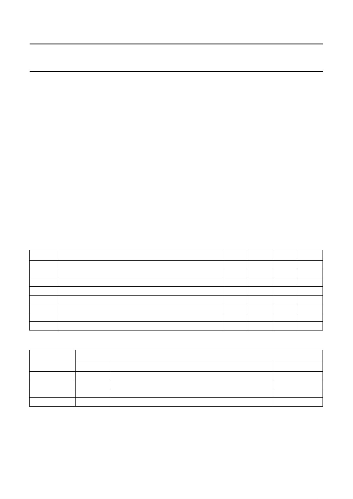
3 QUICK REFERENCE DATA
SYMBOL PARAMETER MIN. TYP. MAX. UNIT
V
DD
I
DD
I
stb
V
HG(RMS)
V
LG(RMS)
G
v
operating supply voltage 2.5 − 6.0 V
operating supply current −−0.9 mA
standby current −−3µA
DTMF HIGH group output voltage level (RMS value) 158 192 205 mV
DTMF LOW group output voltage level (RMS value) 125 150 160 mV
pre-emphasis (voltage gain) of group 1.85 2.10 2.35 dB
THD total harmonic distortion −−25 − dB
T
amb
operating ambient temperature −25 − +70 °C
4 ORDERING INFORMATION
PACKAGE
TYPE NUMBER
NAME DESCRIPTION VERSION
PCD3311CP DIP14 plastic dual in-line package; 14 leads (300 mil) SOT27-1
PCD3311CT SO16 plastic small outline package; 16 leads; body width 7.5 mm SOT162-1
PCD3312CP DIP8 plastic dual in-line package; 8 leads (300 mil) SOT97-1
PCD3312CT SO8 plastic small outline package; 8 leads; body width 7.5 mm SOT176-1
1996 Nov 21 3
Page 4

Philips Semiconductors Product specification
DTMF/modem/musical-tone generators PCD3311C; PCD3312C
5 BLOCK DIAGRAM
handbook, full pagewidth
D5
D4
D3
D2
3
4
12
11
10
9(8)
8(7)
5
MODE
D1/SDA
D0/SCL
STROBE
The un-parenthesised numbers are for the PCD3311CP, those in parenthesis for the PCD3312C.
OSCI OSCO
OSCILLATOR
INPUT
CONTROL
LOGIC
A
0
1(3)
7(6)
2(4)
GENERATOR
HIGH
GROUP
DIVIDER
DIVIDER
SELECTION
(ROM)
LOW
GROUP
DIVIDER
CLOCK
SWITCHED
CAPACITOR
BANDGAP
VOLTAGE
REFERENCE
ADDER
Fig.1 Block diagram.
DAC
HIGH
DAC
LOW
V
DD
14(2) 13(1)
SWITCHED
CAPACITOR
PCD3311C
PCD3312C
V
SS
RESISTOR
CAPACITOR
MGG543
(5)6
TONE
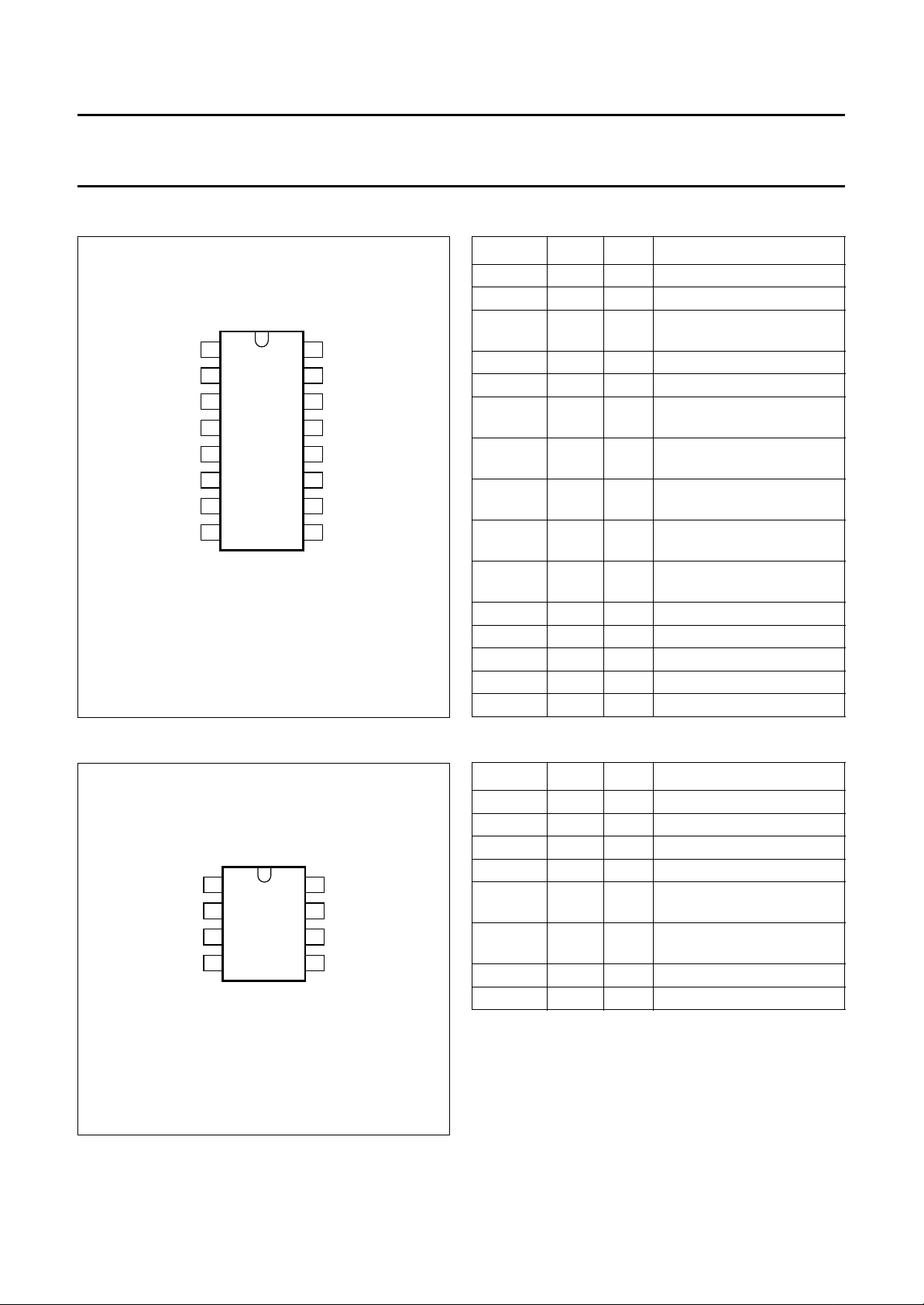
6 PINNING INFORMATION
6.1 Pinning PCD3311CP
handbook, halfpage
OSCI
OSCO
MODE
D5
STROBE
TONE
A0
1
2
3
4
PCD3311CP
5
6
7
Fig.2 Pin configuration PCD3311CP.
MGG508
14
13
12
11
10
9
8
V
DD
V
SS
D4
D3
D2
D1/SDA
D0/SCL
6.2 Pin description PCD3311CP
SYMBOL PIN TYPE DESCRIPTION
OSCI 1 I oscillator input
OSCO 2 O oscillator output
MODE 3 I mode select input (selects
2
C or parallel data input)
I
D5 4 I parallel data input
STROBE 5 I strobe input (for loading
data in parallel mode)
TONE 6 O frequency output (DTMF,
modem, musical tones)
A0 7 I slave address input (to be
connected to V
or VSS)
DD
D0/SCL 8 I parallel data input or
2
C-bus clock line
I
D1/SDA 9 I parallel data input or
2
C-bus data line
I
D2 − D4 10 − 12 I parallel data inputs
V
SS
V
DD
13 P negative supply
14 P positive supply
1996 Nov 21 4
Page 5
Philips Semiconductors Product specification
DTMF/modem/musical-tone generators PCD3311C; PCD3312C
6.3 Pinning PCD3311CT
handbook, halfpage
OSCI
OSCO
MODE
D5
n.c.
STROBE
TONE
A0
1
2
3
4
PCD3311CT
5
6
7
8
Fig.3 Pin configuration PCD3311CT.
MGG509
16
15
14
13
12
11
10
9
V
DD
V
SS
D4
n.c.
D3
D2
D1/SDA
D0/SCL
6.4 Pin description PCD3311CT
SYMBOL PIN TYPE DESCRIPTION
OSCI 1 I oscillator input
OSCO 2 O oscillator output
MODE 3 I mode select input (selects
2
C or parallel data input)
I
D5 4 I parallel data input
n.c. 5 − not connected
STROBE 6 I strobe input (for loading
data in parallel mode)
TONE 7 O frequency output (DTMF,
modem, musical tones)
A0 8 I slave address input (to be
connected to V
or VSS)
DD
D0/SCL 9 I parallel data input or
2
C-bus clock line
I
D1/SDA 10 I parallel data input or
2
C-bus data line
I
D2, D3 11, 12 I parallel data inputs
n.c. 13 − not connected
D4 14 I parallel data input
V
SS
V
DD
15 P negative supply
16 P positive supply
6.5 Pinning PCD3312C
handbook, halfpage
V
SS
V
DD
OSCI
OSCO
1
2
PCD3312C
3
4
Fig.4 Pin configuration PCD3312C.
MGG510
6.6 Pin description PCD3312C
SYMBOL PIN TYPE DESCRIPTION
V
SS
V
DD
1 P negative supply
2 P positive supply
OSCI 3 I oscillator input
OSCO 4 O oscillator output
SDA
8
SCL
7
A0
6
TONE
5
TONE 5 O frequency output (DTMF,
modem, musical tones)
A0 6 I slave address input (to be
or VSS)
DD
SCL 7 I I
SDA 8 I I
connected to V
2
C-bus clock line
2
C-bus data line
1996 Nov 21 5
Page 6
Philips Semiconductors Product specification
DTMF/modem/musical-tone generators PCD3311C; PCD3312C
7 FUNCTIONAL DESCRIPTION
7.1 General (see Fig.1)
The Input Control Logic decodes the input data to
determine whether DTMF, modem or musical tones are
selected; and which particular tone or combination of
tones is required.
A code representing the required tones is sent to the
Divider Selection ROM which selects the correct division
ratio in both of the Frequency Dividers (or in one divider, if
only a single tone is required).
The Oscillator circuit provides a square wave of frequency
3.58 MHz. Each Frequency Divider divides the frequency
of the Oscillator to give a serial digital square wave with a
frequency simply related to that of the required tone.
The output from each Frequency Divider goes to a DAC,
which is also fed by a clock derived from the oscillator.
Using these two signals, the DAC produces an
approximate sine wave of the required frequency, with an
amplitude derived from the Voltage Reference.
The output from the DAC goes to an Adder where, for
DTMF, it is combined with the output from the other DAC.
The output from the Adder goes through two stages of Low
Pass Filters to give a smoothed tone (single or dual), and
finally to the TONE output.
7.4 Data inputs (PCD3311C)
Inputs D0, D1, D2, D3, D4 and D5 are used in the parallel
data input mode of the PCD3311C. Inputs D0 and D1 are
also used in serial input mode when they act as the SCL
and SDA inputs respectively. Inputs D0 and D1 have no
internal pull-down or pull-up resistors and must not be left
open in any application. Inputs D2, D3, D4 and D5 have
internal pull-down.
D4 and D5 are used to select between DTMF dual, DTMF
single, modem and musical tones (see Table 1). D0, D1,
D2 and D3 select the tone combination or single tone
within the selected application. They also, in combination
with D4, select the standby mode. See Tables 2, 3, 4
and 5.
PCD 3312C has no parallel data pins as data input is via
2
C-bus.
the I
Table 1 Use of D5 and D4 to select application
D5 D4 APPLICATION
LOW LOW DTMF single tones; musical tones;
standby
LOW HIGH DTMF dual tones (all 16 combinations)
HIGH LOW modem tones
HIGH HIGH musical tones
7.2 Clock/oscillator connection
The timebase for the PCD3311C and PCD3312C is a
crystal-controlled oscillator, requiring a 3.58 MHz quartz
crystal to be connected between OSCI and OSCO.
Alternatively, the OSCI input can be driven from an
external clock of 3.58 MHz.
7.3 Mode selection (PCD3311C)
The MODE input selects the data input mode for the
PCD3311C. When MODE is connected to V
(HIGH),
DD
data can be received in the parallel mode. When
connected to VSS (LOW) or left open, data can be received
via the serial I2C-bus.
PCD 3312C has no MODE input as data input is via the
I2C-bus only.
7.5 Strobe input (PCD3311C )
The STROBE input (with internal pull-down) allows the
loading of parallel data into D0 to D5 when MODE is HIGH.
The data inputs must be stable preceding the
positive-going edge of the strobe pulse (active HIGH).
Input data are loaded at the negative-going edge of the
strobe pulse and then the corresponding tone (or standby
mode) is provided at the TONE output. The output remains
unchanged until the negative-going edge of the next
STROBE pulse (for new data) is received. Figure 5 is an
example of the timing relationship between STROBE and
the data inputs.
When MODE is LOW, data is received serially via the
2
C-bus.
I
1996 Nov 21 6
Page 7

Philips Semiconductors Product specification
DTMF/modem/musical-tone generators PCD3311C; PCD3312C
90%
t
SPW
t
DH
oscillator OFF
t
(ON)
tone
oscillator ON
no output tone
oscillator ON
output tones
handbook, full pagewidth
STROBE
TONE
10%
t
DS
D0
D1
D2
D3
D4
D5
MGG511
Fig.5 Timing of STROBE, parallel data inputs and TONE output (770 Hz + 1477 Hz in example) in the parallel
mode (MODE = HIGH).
7.6 I2C-bus clock and data inputs
SCL and SDA are the serial clock and serial data inputs
according to the I2C-bus specification, see Chapter 8.
SCL and SDA must be pulled up externally to VDD.
For the PCD3311C, SCL and SDA are combined with
parallel inputs D0 and D1 respectively - D0/SCL and
D1/SDA operate serially only when MODE is LOW.
7.7 Address input
Address input A0 defines the least significant bit of the
2
C-bus address of the device (see Fig.6). The first 6 bits
I
of the address are fixed internally. By tying the A0 of each
device to VDD (HIGH) and VSS(LOW) respectively, two
different PCD3311C or PCD3312C devices can be
individually addressed on the bus.
Whether one or two devices are used, A0 must be
connected to VDD or VSS.
1996 Nov 21 7
7.8 I
2
C-bus data configuration (see Fig.6)
The PCD3311C and PCD3312C are always slave
receivers in the I2C-bus configuration. The R/W bit in is
thus always LOW, indicating that the master
(microcontroller) is writing.
The slave address in the serial mode consists of 7 bits: 6
bits internally fixed, 1 externally set via A0. in the serial
mode, the same input data codes are used as in the
parallel mode. See Tables 2, 3, 4 and 5.
7.9 Tone output
The single and dual tones provided at the TONE output are
first filtered by an on-chip switched-capacitor filter,
followed by an active RC low-pass filter. The filtered tones
fulfil the CEPT recommendations for total harmonic
distortion of DTMF tones. An on-chip reference voltage
provides output tone levels independent of the supply
voltage. Tables 3, 4 and 5 give the frequency deviation of
the output tones with respect to the standard DTMF,
modem and music frequencies.
Page 8

Philips Semiconductors Product specification
DTMF/modem/musical-tone generators PCD3311C; PCD3312C
handbook, full pagewidth
acknowledge
from slave
MSB
S 010010A00AXXD5D4D3D2D1D0AP
slave address data
MGG512
R/W
acknowledge
from slave
internal STROBE
for data latching
Fig.6 I2C-bus data format.
7.10 Power-on reset
In order to avoid an undefined state when the power is switched ON, the devices have an internal reset circuit which sets
the standby mode (oscillator OFF).
7.11 TABLES OF INPUT AND OUTPUT
The specified output tones are obtained when a 3.579545 MHz crystal is used.
In each table, the logical states for the input data lines are related to voltage levels as follows:
1 = HIGH = V
0 = LOW = V
DD
SS
X = don’t care
Table 2 Input data for no output tone, TONE in 3-state
D5 D4 D3 D2 D1 D0 HEX
(1)
X 0 0 0 0 0 00 or 20 ON
X 0 0 0 0 1 01 or 21 OFF
X 0 0 0 1 0 02 or 22 OFF
X 0 0 0 1 1 03 or 23 OFF
Note
1. The alternative HEX values depend on the value of D5.
1996 Nov 21 8
OSCILLATOR
Page 9

Philips Semiconductors Product specification
DTMF/modem/musical-tone generators PCD3311C; PCD3312C
Table 3 Input data and output for DTMF tones
STANDARD
D5 D4 D3 D2 D1 D0 HEX SYMBOL
00100008 − 697 697.90 +0.13 +0.90
00100109 − 770 770.46 +0.06 +0.46
0010100A − 852 850.45 −0.18 −1.55
0010110B − 941 943.23 +0.24 +2.23
0011000C − 1209 1206.45 −0.21 −2.55
0011010D − 1336 1341.66 +0.42 +5.66
0011100E − 1477 1482.21 +0.35 +5.21
0011110F − 1633 1638.24 +0.32 +5.24
01000010 0 941+1336 −−−
01000111 1 697+1209 −−−
01001012 2 697+1336 −−−
01001113 3 697+1477 −−−
01010014 4 770+1209 −−−
01010115 5 770+1336 −−−
01011016 6 770+1477 −−−
01011117 7 852+1209 −−−
01100018 8 852+1336 −−−
01100119 9 852+1477 −−−
0110101A A697+1633 −−−
0110111B B770+1633 −−−
0111001C C852+1633 −−−
0111011D D941+1633 −−−
0111101E * 941+1209 −−−
0111111F # 941+1477 −−−
FREQUENCY
Hz Hz % Hz
TONE
OUTPUT
FREQ.
FREQUENCY
DEVIATION
Table 4 Input data and output for modem tones
STANDARD
D5 D4 D3 D2 D1 D0 HEX
10010024 13001296.94 −0.24 −3.06
10010125 21002103.14 +0.15 +3.14
10011026 12001197.17 −0.24 −2.83
10011127 22002192.01 −0.36 −7.99
10100028 980978.82 −0.12 −1.18
10100129 11801179.03 −0.08 −0.97
1996 Nov 21 9
FREQUENCY
Hz Hz % Hz
TONE
OUTPUT
FREQ.
FREQUENCY
DEVIATION
TELECOM.
STANDARD
V.23
Bell 202
V.21
Page 10

Philips Semiconductors Product specification
DTMF/modem/musical-tone generators PCD3311C; PCD3312C
STANDARD
D5 D4 D3 D2 D1 D0 HEX
1010102A 10701073.33 +0.31 +3.33
1010112B 12701265.30 −0.37 −4.70
1011002C 16501655.66 +0.34 +5.66
1011012D 18501852.77 +0.15 +2.77
1011102E 20252021.20 −0.19 −3.80
1011112F 22252223.32 −0.08 −1.68
Table 5 Input/output for musical tones
D5 D4 D3 D2 D1 D0 HEX NOTE
11000030 D#5 622.3 622.5
11000131 E5 659.3 659.5
11001032 F5 698.5 697.9
11001133 F#5 740.0 741.1
11010034 G5 784.0 782.1
11010135 G#5 830.6 832.3
11011036 A5 880.0 879.3
11011137 A#5 932.3 931.9
11100038 B5 987.8 985.0
11100139 C6 1046.5 1044.5
1110103A C#6 1108.7 1111.7
10100129 D6 1174.7 1179.0
1110113B D#6 1244.5 1245.1
1111003C E6 1318.5 1318.9
1111013D F6 1396.9 1402.1
0011100E F#6 1480.0 1482.2
1111103E G6 1568.0 1572.0
1011002C G#6 1661.2 1655.7
1111113F A6 1760.0 1768.5
00010004 A#6 1864.7 1875.1
00010105 B6 1975.5 1970.0
10010125 C7 2093.0 2103.1
1011112F C#7 2217.5 2223.3
00111006 D7 2349.3 2358.1
00011107 D#7 2489.0 2470.4
FREQUENCY
Hz Hz % Hz
TONE
OUTPUT
FREQ.
FREQUENCY
DEVIATION
STD. FREQ.
BASED ON
A4 = 440 Hz
Hz Hz
FREQUENCY
TELECOM.
STANDARD
Bell 103
V.21
Bell 103
TONE
OUTPUT
1996 Nov 21 10
Page 11

Philips Semiconductors Product specification
DTMF/modem/musical-tone generators PCD3311C; PCD3312C
8I2C-BUS INTERFACE
The I2C-bus is for two-way communication between different ICs or modules. It uses only two lines, a serial data line
(SDA) and a serial clock line (SCL), both of which are bi-directional. Both lines must be connected to a positive supply
via a pull-up resistor when connected to the output stages of a device. Data transfer may be initiated only when the bus
is not busy.
8.1 Bit transfer (see Fig.7)
One data bit is transferred during each clock pulse. The data on the SDA line must remain stable during the HIGH period
of the clock pulse as changes in the data line at this time will be interpreted as control signals.
SDA
SCL
data line
stable;
data valid
change
of data
allowed
MBC621
Fig.7 Bit transfer.
8.2 Start and stop conditions (see Fig.8)
Both data and clock lines remain HIGH when the bus is not busy. A HIGH-to-LOW transition of the data line, while the
clock is HIGH is defined as the start condition (S). A LOW-to-HIGH transition of the data line while the clock is HIGH is
defined as the stop condition (P).
SDA
SCL
S
START condition
P
STOP condition
SDA
SCL
MBC622
Fig.8 Start and stop conditions.
1996 Nov 21 11
Page 12

Philips Semiconductors Product specification
DTMF/modem/musical-tone generators PCD3311C; PCD3312C
8.3 System configuration (see Fig.9)
A device generating a message is a ‘transmitter’, a device receiving a message is the ‘receiver’. The device that controls
message transfer is the ‘master’ and the devices that are controlled by the master are the ‘slaves’.
SDA
SCL
MASTER
TRANSMITTER /
RECEIVER
SLAVE
RECEIVER
SLAVE
TRANSMITTER /
RECEIVER
MASTER
TRANSMITTER
MASTER
TRANSMITTER /
RECEIVER
MBA605
Fig.9 System configuration.
8.4 Acknowledge
The number of data bytes transferred between the start and stop conditions from transmitter to receiver is not limited.
Each byte of eight bits is followed by one acknowledge bit. The acknowledge bit is a HIGH level put on the bus by the
transmitter whereas the master generates an extra acknowledge after the reception of each byte. Also a master must
generate an acknowledge after reception of each byte that has been clocked out of the slave transmitter. The device that
acknowledges has to pull down the SDA line during the acknowledge-related clock pulse. Set-up and hold times must
be taken into account to ensure that the SDA line is stable LOW during the whole HIGH period of the
acknowledge-related clock pulse. A master receiver must signal an end of data to the transmitter by not generating an
acknowledge on the last byte that has been clocked out of the slave. In this event the transmitter must leave the data
line HIGH to enable the master to generate the stop condition.
DATA OUTPUT
BY TRANSMITTER
DATA OUTPUT
BY RECEIVER
SCL FROM
MASTER
S
START
CONDITION
Fig.10 Acknowledgment on the I2C-bus.
1996 Nov 21 12
not acknowledge
acknowledge
MBC602
9821
clock pulse for
acknowledgement
Page 13

Philips Semiconductors Product specification
DTMF/modem/musical-tone generators PCD3311C; PCD3312C
8.5 Timing specifications
The PCD3311C and PCD3312C accept data input from a microcontroller and are ‘slave receivers’ when operating via
the I2C-bus. They support the ‘standard’ and ‘low-speed’ modes of the I2C-bus, but not the ‘fast’ mode detailed in
I2C-bus and how to use it”
document order no. 9398 393 40011. The timing requirements for the devices are described
in Sections 8.5.1 and 8.5.2.
“The
8.5.1 S
TANDARD MODE
Masters generate a bus clock with a maximum frequency of 100 kHz. Detailed timing is shown in Fig.11, where the two
signal levels are LOW = VIL and HIGH = VIH, see Chapter 11. Figure 12 shows a complete data transfer in standard
mode. The time symbols are explained in Table 6.
handbook, full pagewidth
SDA
t
HIGH
t
f
t
SU;DAT
t
SU;STO
SCL
SDA
MBC764
t
BUF
t
HD;STA
t
LOW
t
r
t
SU;STA
t
HD;DAT
Fig.11 Standard mode timing.
1996 Nov 21 13
Page 14

Philips Semiconductors Product specification
DTMF/modem/musical-tone generators PCD3311C; PCD3312C
handbook, full pagewidth
Clock LOW minimum = 4.7 µs; clock HIGH minimum = 4 µs.
The dashed line is the acknowledgment of the receiver.
Mark-to-space ratio = 1 : 1 (LOW-to-HIGH).
Maximum number of bytes is unrestricted.
Premature termination of transfer is allowed by generation of STOP condition.
Acknowledge clock bit must be provided by master.
SDA
SCL
CONDITION
981 - 7981 - 7981 - 7
ACKADDRESS R/W
DATASTART
ACK
CONDITION
START
STOPACKADDRESS R/W
MBC765
Fig.12 Complete data transfer in standard mode.
Table 6 Explanation of time symbols used in Fig.11
SYMBOL PARAMETER REMARKS MIN. MAX. UNIT
f
t
t
SCL
SW
BUF
SCL clock frequency 0 100 kHz
tolerable pulse spike width − 100 ns
bus free time The time that the bus is free (SDA is HIGH)
4.7 −µs
before a new transmission is initiated by SDA
going LOW.
t
SU;STA
t
HD;STA
set-up time repeated START Only valid for repeated start code. 4.7 −µs
hold time ST ART condition The time between SDA going LOW and the first
4.0 −µs
valid negative-going transition of SCL.
t
LOW
t
HIGH
t
r
t
f
t
SU;DAT
t
HD;DAT
t
SU;STO
SCL LOW time The LOW period of the SCL clock. 4.7 −µs
SCL HIGH time The HIGH period of the SCL clock. 4.0 −µs
rise time SDA and SCL − 1.0 µs
fall time SDA and SCL − 0.3 µs
data set-up time 250 − ns
data hold time 0 − ns
set-up time STOP condition 4.0 −µs
8.5.2 L
OW-SPEED MODE
Masters generate a bus clock with a maximum frequency of 2 kHz; a minimum LOW period of 105 µs and a minimum
HIGH period of 365 µs. The mark-to-space ratio is 1 : 3 LOW-to-HIGH. Detailed timing is shown in Fig.13, where the two
signal levels are LOW = VIL and HIGH = VIH, see Chapter 11. Figure 14 shows a complete data transfer in low-speed
mode.The time symbols are explained in Table 7.
1996 Nov 21 14
Page 15

Philips Semiconductors Product specification
DTMF/modem/musical-tone generators PCD3311C; PCD3312C
handbook, full pagewidth
SDA
SCL
SDA
handbook, full pagewidth
SDA
t
BUF
t
HD;STA
t
LOW
t
r
t
SU;STA
t
HIGH
Fig.13 Low-speed mode timing.
t
f
t
SU;DAT
t
HD;DAT
t
SU;STO
MGG545
R/W
SCL
START
CONDITION
Clock LOW minimum = 130 µs ±25 µs; clock HIGH minimum 390 µs ±25 µs.
Mark-to-space ratio = 1 : 3 (LOW-to-HIGH).
Start byte 0000 0001.
Maximum number of bytes = 6.
Premature termination of transfer not allowed.
Acknowledge clock bit must be provided by master.
START BYTE DUMMY
ACKNOWLEDGE
Fig.14 Complete data transfer in low speed mode.
1996 Nov 21 15
REPEATED
START
CONDITION
ADDRESS
ACKNOWLEDGE STOP
CONDITION
MGG546
Page 16

Philips Semiconductors Product specification
DTMF/modem/musical-tone generators PCD3311C; PCD3312C
Table 7 Explanation of time symbols used in Fig.13
SYMBOL PARAMETER REMARKS MIN. MAX. UNIT
f
SCL
t
SW
t
BUF
t
SU;STA
t
HD;STA
t
LOW
t
HIGH
t
r
t
f
t
SU;DAT
t
HD;DAT
t
SU;STO
SCL clock frequency 0 2 kHz
tolerable pulse spike width − 100 ns
bus free time The time that the bus is free (SDA is
105 −µs
HIGH) before a new transmission is
initiated by SDA going LOW.
set-up time repeated START Only valid for repeated start code. 105 155 µs
hold time START condition The time between SDA going LOW and
365 415 µs
the first valid negative-going transition of
SCL.
SCL LOW time The LOW period of the SCL clock. 105 155 µs
SCL HIGH time The HIGH period of the SCL clock. 365 −µs
rise time SDA and SCL − 1.0 µs
fall time SDA and SCL − 0.3 µs
data set-up time 250 − ns
data hold time 0 − ns
set-up time STOP condition 105 155 µs
9 HANDLING
Inputs and outputs are protected against electrostatic discharge in normal handling. However, it is good practice to take
normal precautions appropriate to handling MOS devices (see
devices”
).
“Handbook IC03, Section: General, Handling MOS
1996 Nov 21 16
Page 17

Philips Semiconductors Product specification
DTMF/modem/musical-tone generators PCD3311C; PCD3312C
10 LIMITING VALUES
In accordance with the Absolute Maximum Rating System (IEC 134).
SYMBOL PARAMETER MIN. MAX. UNIT
V
V
I
I
P
P
I
I
T
T
DD
I
I
O
tot
O
DD
SS
stg
amb
supply voltage −0.8 +8.0 V
all input voltages −0.8 VDD+ 0.8 V
DC input current −10 +10 mA
DC output current −10 +10 mA
total power dissipation − 300 mW
power dissipation per output − 50 mW
supply current through pin V
supply current through pin V
DD
SS
−50 +50 mA
−50 +50 mA
storage temperature −65 +150 °C
operating ambient temperature −25 +70 °C
11 CHARACTERISTICS
= 2.5 to 6.0 V; VSS=0V; T
V
DD
= −25 to +70 °C; all voltages with respect to VSS; f
amb
= 3.58 MHz (gmL);
xtal
maximum series resistance = 50 Ω; unless otherwise specified.
SYMBOL PARAMETER MIN. TYP MAX. UNIT
V
I
DD
DD
operating supply voltage 2.5 − 6.0 V
operating supply current (note 1)
no output tone − 50 100 µA
single output tone − 0.5 0.8 mA
dual output tone − 0.6 0.9 mA
I
stb
static standby current (note 2) −−3µA
Inputs/outputs (SDA)
TO D5; MODE; STROBE
D0
V
IL
V
IH
LOW level input voltage 0 − 0.3V
HIGH level input voltage 0.7V
DD
− V
DD
DD
V
V
D2 TO D5 MODE; STROBE; A0
I
IL
pull-down input current; VI=V
DD
−30 −150 −300 nA
SCL (D0); SDA (D1)
I
OL
f
SCL
C
i
t
i
LOW level output current (SDA); VOL= 0.4 V 3 −−mA
SCL clock frequency −−100 kHz
input capacitance; VI=V
SS
−−7pF
allowable input spike pulse width −−100 ns
1996 Nov 21 17
Page 18

Philips Semiconductors Product specification
DTMF/modem/musical-tone generators PCD3311C; PCD3312C
SYMBOL PARAMETER MIN. TYP MAX. UNIT
TONE output (see test circuit, Fig.15)
V
HG(RMS)
V
LG(RMS)
V
DC
G
v
THD Total Harmonic Distortion; T
output impedance − 0.1 0.5 kΩ
Z
o
OSCI input
V
OSC(p-p)
Timing (V
t
OSC(ON)
t
TONE(ON)
t
SPW
t
DS
t
DH
Notes
1. Oscillator ON; VDD= 3 V; crystal connected between OSCI and OSCO; D0/SCL and D1/SDA connected via
resistance of 5.6 kΩ to VDD; all other pins left open.
2. As note 1, but with oscillator OFF.
3. Related to the level of the LOW group frequency component, according to CEPT recommendations.
4. Related to the level of the fundamental frequency.
5. Oscillator must be running.
6. Values are referenced to the 10% and 90% levels of the relevant pulse amplitudes, with a total voltage swing from
VSSto VDD.
DTMF output voltage (RMS), HIGH group 158 192 205 mV
DTMF output voltage (RMS), LOW group 125 150 160 mV
DC voltage level −
1
⁄2V
DD
− V
voltage gain (pre-emphasis) of group 1.85 2.10 2.35 dB
=25°C
amb
dual tone (note 3) −−25 − dB
modem tone (note 4) −−29 − dB
maximum allowable amplitude at OSCI −−V
=3V)
DD
− VSSV
DD
oscillator start-up time − 3 − ms
TONE start-up time (note 5) − 0.5 − ms
STROBE pulse width (note 6) 400 −−ns
data set-up time (note 6) 150 −−ns
data hold time (note 6) 100 −−ns
handbook, halfpage
V
DD
PCD3311C
PCD3312C
TONE
V
SS
Fig.15 TONE output test circuit.
1996 Nov 21 18
1 µF
50 pF
10 kΩ
MGG513
Page 19

Philips Semiconductors Product specification
DTMF/modem/musical-tone generators PCD3311C; PCD3312C
1.6
handbook, halfpage
I
stb
(µA)
1.2
0.8
0.4
0
0
2
4
T
amb
−25 ˚C
+25 ˚C
+70 ˚C
68
V
DD
Fig.16 Standby supply current as a function of
supply voltage; oscillator OFF.
MGG514
=
(V)
300
handbook, halfpage
I
DD
(µA)
200
100
0
0
24 86
MGG515
T
amb
−25 ˚C
+25 ˚C
+70 ˚C
VDD (V)
Fig.17 Operating supply current as a function of
supply voltage; oscillator ON, no output at
TONE.
=
1.5
handbook, halfpage
I
DD
(mA)
1
0.5
0
0
24 86
MGG516
T
amb
−25 ˚C
+25 ˚C
+70 ˚C
VDD (V)
=
Fig.18 Operating supply current as a function of
supply voltage; oscillator ON, dual tone at
TONE.
1996 Nov 21 19
I
(µA)
6
I
4
2
0
T
= −25 ˚C
amb
+70 ˚C
0
+25 ˚C
123
VI (V)
handbook, halfpage
Fig.19 Pull-down input current as a function of
input voltage; VDD=3V.
MGG517
Page 20

Philips Semiconductors Product specification
DTMF/modem/musical-tone generators PCD3311C; PCD3312C
−11
handbook, halfpage
V
TONE
(dBm)
−12
T
amb
−25 ˚C
+25 ˚C
=
HIGH GROUP
MGG518
+70 ˚C
−13
−14
−25 ˚C
+25 ˚C
LOW GROUP
+70 ˚C
−15
0246
VDD (V)
Fig.20 DTMF output voltage levels as a function of
operating supply voltage; RL=1MΩ.
handbook, full pagewidth
level
(dBm)
0
−20
−40
0.4
handbook, halfpage
V
TONE
MGG519
(dB)
T
=
0
amb
−25 ˚C
+25 ˚C
−0.4
+70 ˚C
−0.8
6
10
5
10
4
10
RL (Ω)
Fig.21 Dual tone output voltage level as a function
of output load resistance.
MGG520
CS203
3
10
−60
−80
−100
012345
handbook, full pagewidth
0
level
(dBm)
−20
−40
−60
−80
−100
01020304050
Fig.22 Typical frequency spectrum of a dual tone signal after flat-band amplification of 6 dB.
1996 Nov 21 20
frequency (kHz)
MGG521
CS203
frequency (kHz)
Page 21

Philips Semiconductors Product specification
DTMF/modem/musical-tone generators PCD3311C; PCD3312C
12 APPLICATION INFORMATION
handbook, halfpage
3A21
6B54
9C87
D0
V
MICROCONTROLLER
SS
GENERAL
PURPOSE
(4 or 8-BIT)
V
DD
mute
data bus
OSCI OSCO STROBE
D0
D5
MODE
PCD3311C
TONE
V
V
DD
SS
MBH669
Fig.23 PCD3311C driven by microcontroller with parallel data bus.
handbook, halfpage
3A21
6B54
9C87
D0
V
TELEPHONY
MICROCONTROLLER
V
SS
PCF84C21A
DD
mute
OSCI OSCO
3.58 MHz
2
I
C bus
4 pF
OSCI OSCO
SCL
SDA
PCD3312C
A
0
TONE
V
V
DD
SS
MGG544
Fig.24 PCD3312C driven by microcontroller PCF84C21A. The PCF84C21A is a single-chip 8-bit microcontroller
with 2 kbytes ROM and I2C-bus. The same application is possible with the PCD3311C with MODE = VSS.
1996 Nov 21 21
Page 22

Philips Semiconductors Product specification
DTMF/modem/musical-tone generators PCD3311C; PCD3312C
13 PACKAGE OUTLINES
DIP14: plastic dual in-line package; 14 leads (300 mil)
D
seating plane
L
Z
14
pin 1 index
e
b
SOT27-1
M
E
A
2
A
A
1
w M
b
1
8
E
c
(e )
1
M
H
1
0 5 10 mm
scale
DIMENSIONS (inch dimensions are derived from the original mm dimensions)
A
A
A
UNIT
inches
Note
1. Plastic or metal protrusions of 0.25 mm maximum per side are not included.
max.
mm
OUTLINE
VERSION
SOT27-1
1 2
min.
max.
1.73
1.13
0.068
0.044
IEC JEDEC EIAJ
050G04 MO-001AA
b
b
1
0.53
0.38
0.021
0.015
0.36
0.23
0.014
0.009
REFERENCES
cD
(1) (1)
19.50
18.55
0.77
0.73
1996 Nov 21 22
7
L
Ee M
6.48
6.20
0.26
0.24
e
1
3.60
3.05
0.14
0.12
M
E
8.25
7.80
0.32
0.31
EUROPEAN
PROJECTION
H
10.0
8.3
0.39
0.33
w
max.
0.2542.54 7.62
0.010.10 0.30
0.0870.17 0.020 0.13
ISSUE DATE
92-11-17
95-03-11
(1)
Z
2.24.2 0.51 3.2
Page 23

Philips Semiconductors Product specification
DTMF/modem/musical-tone generators PCD3311C; PCD3312C
SO16: plastic small outline package; 16 leads; body width 7.5 mm
D
c
y
Z
16
pin 1 index
1
e
9
A
2
A
8
w M
b
p
SOT162-1
E
H
E
Q
1
L
p
L
detail X
(A )
A
X
v M
A
A
3
θ
0 5 10 mm
scale
DIMENSIONS (inch dimensions are derived from the original mm dimensions)
mm
OUTLINE
VERSION
SOT162-1
A
max.
2.65
0.10
A
0.30
0.10
0.012
0.004
A2A
1
2.45
2.25
0.096
0.089
IEC JEDEC EIAJ
075E03 MS-013AA
0.25
0.01
b
3
p
0.49
0.32
0.36
0.23
0.019
0.013
0.014
0.009
UNIT
inches
Note
1. Plastic or metal protrusions of 0.15 mm maximum per side are not included.
(1)E(1) (1)
cD
10.5
7.6
7.4
0.30
0.29
1.27
0.050
10.1
0.41
0.40
REFERENCES
1996 Nov 21 23
eHELLpQ
10.65
10.00
0.42
0.39
1.4
0.055
1.1
0.4
0.043
0.016
1.1
1.0
0.043
0.039
PROJECTION
0.25
0.25 0.1
0.01
0.01
EUROPEAN
ywv θ
Z
0.9
0.4
8
0.004
ISSUE DATE
0.035
0.016
92-11-17
95-01-24
0
o
o
Page 24

Philips Semiconductors Product specification
DTMF/modem/musical-tone generators PCD3311C; PCD3312C
DIP8: plastic dual in-line package; 8 leads (300 mil)
D
seating plane
A
L
Z
e
b
8
pin 1 index
1
w M
b
1
b
2
5
SOT97-1
M
E
A
2
A
c
(e )
1
M
H
E
1
4
0 5 10 mm
scale
DIMENSIONS (inch dimensions are derived from the original mm dimensions)
A
A
A
UNIT
mm
inches
max.
12
min.
max.
b
1.73
1.14
0.068
0.045
b
1
0.53
0.38
0.021
0.015
b
1.07
0.89
0.042
0.035
cD E e M
2
0.36
0.23
0.014
0.009
9.8
9.2
0.39
0.36
Note
1. Plastic or metal protrusions of 0.25 mm maximum per side are not included.
OUTLINE
VERSION
SOT97-1
IEC JEDEC EIAJ
050G01 MO-001AN
REFERENCES
1996 Nov 21 24
(1) (1)
6.48
6.20
0.26
0.24
L
3.60
3.05
0.14
0.12
M
8.25
7.80
0.32
0.31
E
10.0
0.39
0.33
e
1
EUROPEAN
PROJECTION
H
8.3
w
max.
0.2542.54 7.62
1.154.2 0.51 3.2
0.010.10 0.30
0.0450.17 0.020 0.13
ISSUE DATE
(1)
Z
92-11-17
95-02-04
Page 25

Philips Semiconductors Product specification
DTMF/modem/musical-tone generators PCD3311C; PCD3312C
SO8: plastic small outline package; 8 leads; body width 7.5 mm
D
c
y
Z
8
pin 1 index
1
e
5
A
2
A
1
4
w M
b
p
E
H
E
detail X
SOT176-1
A
X
v M
A
Q
(A )
L
p
L
A
3
θ
0 5 10 mm
scale
DIMENSIONS (inch dimensions are derived from the original mm dimensions)
UNIT
mm
inches
Note
1. Plastic or metal protrusions of 0.15 mm maximum per side are not included.
A
max.
2.65
0.10
OUTLINE
VERSION
SOT176-1
A1A2A3b
0.3
2.45
0.1
0.012
0.004
0.25
2.25
0.096
0.01
0.089
IEC JEDEC EIAJ
p
0.49
0.36
0.019
0.014
0.32
0.23
0.013
0.009
(1)E(1)
cD
7.65
7.45
0.30
0.29
REFERENCES
7.6
7.4
0.30
0.29
1.27
0.050
1996 Nov 21 25
eHELLpQywv θ
1.45
0.057
1.1
0.45
0.043
0.018
1.1
1.0
0.043
0.039
0.25 0.1
0.25
0.01 0.004
0.01
EUROPEAN
PROJECTION
10.65
10.00
0.42
0.39
(1)
Z
2.0
1.8
0.079
0.071
ISSUE DATE
91-08-13
95-02-25
o
8
o
0
Page 26

Philips Semiconductors Product specification
DTMF/modem/musical-tone generators PCD3311C; PCD3312C
14 SOLDERING
14.1 Introduction
There is no soldering method that is ideal for all IC
packages. Wave soldering is often preferred when
through-hole and surface mounted components are mixed
on one printed-circuit board. However, wave soldering is
not always suitable for surface mounted ICs, or for
printed-circuits with high population densities. In these
situations reflow soldering is often used.
This text gives a very brief insight to a complex technology.
A more in-depth account of soldering ICs can be found in
our
“IC Package Databook”
(order code 9398 652 90011).
14.2 DIP
14.2.1 S
OLDERING BY DIPPING OR BY WA VE
The maximum permissible temperature of the solder is
260 °C; solder at this temperature must not be in contact
with the joint for more than 5 seconds. The total contact
time of successive solder waves must not exceed
5 seconds.
The device may be mounted up to the seating plane, but
the temperature of the plastic body must not exceed the
specified maximum storage temperature (T
stg max
). If the
printed-circuit board has been pre-heated, forced cooling
may be necessary immediately after soldering to keep the
temperature within the permissible limit.
14.2.2 R
EPAIRING SOLDERED JOINTS
Apply a low voltage soldering iron (less than 24 V) to the
lead(s) of the package, below the seating plane or not
more than 2 mm above it. If the temperature of the
soldering iron bit is less than 300 °C it may remain in
contact for up to 10 seconds. If the bit temperature is
between 300 and 400 °C, contact may be up to 5 seconds.
14.3 SO
14.3.1 REFLOW SOLDERING
Reflow soldering techniques are suitable for all SO
packages.
Several techniques exist for reflowing; for example,
thermal conduction by heated belt. Dwell times vary
between 50 and 300 seconds depending on heating
method. Typical reflow temperatures range from
215 to 250 °C.
Preheating is necessary to dry the paste and evaporate
the binding agent. Preheating duration: 45 minutes at
45 °C.
14.3.2 W
AVE SOLDERING
Wave soldering techniques can be used for all SO
packages if the following conditions are observed:
• A double-wave (a turbulent wave with high upward
pressure followed by a smooth laminar wave) soldering
technique should be used.
• The longitudinal axis of the package footprint must be
parallel to the solder flow.
• The package footprint must incorporate solder thieves at
the downstream end.
During placement and before soldering, the package must
be fixed with a droplet of adhesive. The adhesive can be
applied by screen printing, pin transfer or syringe
dispensing. The package can be soldered after the
adhesive is cured.
Maximum permissible solder temperature is 260 °C, and
maximum duration of package immersion in solder is
10 seconds, if cooled to less than 150 °C within
6 seconds. Typical dwell time is 4 seconds at 250 °C.
A mildly-activated flux will eliminate the need for removal
of corrosive residues in most applications.
14.3.3 R
EPAIRING SOLDERED JOINTS
Fix the component by first soldering two diagonallyopposite end leads. Use only a low voltage soldering iron
(less than 24 V) applied to the flat part of the lead. Contact
time must be limited to 10 seconds at up to 300 °C. When
using a dedicated tool, all other leads can be soldered in
one operation within 2 to 5 seconds between
270 and 320 °C.
Reflow soldering requires solder paste (a suspension of
fine solder particles, flux and binding agent) to be applied
to the printed-circuit board by screen printing, stencilling or
pressure-syringe dispensing before package placement.
1996 Nov 21 26
Page 27

Philips Semiconductors Product specification
DTMF/modem/musical-tone generators PCD3311C; PCD3312C
15 DEFINITIONS
Data sheet status
Objective specification This data sheet contains target or goal specifications for product development.
Preliminary specification This data sheet contains preliminary data; supplementary data may be published later.
Product specification This data sheet contains final product specifications.
Limiting values
Limiting values given are in accordance with the Absolute Maximum Rating System (IEC 134). Stress above one or
more of the limiting values may cause permanent damage to the device. These are stress ratings only and operation
of the device at these or at any other conditions above those given in the Characteristics sections of the specification
is not implied. Exposure to limiting values for extended periods may affect device reliability.
Application information
Where application information is given, it is advisory and does not form part of the specification.
16 LIFE SUPPORT APPLICATIONS
These products are not designed for use in life support appliances, devices, or systems where malfunction of these
products can reasonably be expected to result in personal injury. Philips customers using or selling these products for
use in such applications do so at their own risk and agree to fully indemnify Philips for any damages resulting from such
improper use or sale.
17 PURCHASE OF PHILIPS I
Purchase of Philips I
components in the I2C system provided the system conforms to the I2C specification defined by
Philips. This specification can be ordered using the code 9398 393 40011.
2
C COMPONENTS
2
C components conveys a license under the Philips’ I2C patent to use the
1996 Nov 21 27
Page 28

Philips Semiconductors – a worldwide company
Argentina: see South America
Australia: 34 Waterloo Road, NORTH RYDE, NSW 2113,
Tel. +61 2 9805 4455, Fax. +61 2 9805 4466
Austria: Computerstr. 6, A-1101 WIEN, P.O. Box 213,
Tel. +43 1 60 101, Fax. +43 1 60 101 1210
Belarus: Hotel Minsk Business Center, Bld. 3, r. 1211, Volodarski Str. 6,
220050 MINSK, Tel. +375 172 200 733, Fax. +375 172 200 773
Belgium: see The Netherlands
Brazil: seeSouth America
Bulgaria: Philips Bulgaria Ltd., Energoproject, 15thfloor,
51 James Bourchier Blvd., 1407 SOFIA,
Tel. +359 2 689 211, Fax. +359 2 689 102
Canada: PHILIPS SEMICONDUCTORS/COMPONENTS,
Tel. +1 800 234 7381
China/Hong Kong: 501 Hong Kong Industrial Technology Centre,
72 Tat Chee Avenue, Kowloon Tong, HONG KONG,
Tel. +852 2319 7888, Fax. +852 2319 7700
Colombia: see South America
Czech Republic: see Austria
Denmark: Prags Boulevard 80, PB 1919, DK-2300 COPENHAGEN S,
Tel. +45 32 88 2636, Fax. +45 31 57 1949
Finland: Sinikalliontie 3, FIN-02630 ESPOO,
Tel. +358 9 615800, Fax. +358 9 61580/xxx
France: 4 Rue du Port-aux-Vins, BP317, 92156 SURESNES Cedex,
Tel. +33 1 40 99 6161, Fax. +33 1 40 99 6427
Germany: Hammerbrookstraße 69, D-20097 HAMBURG,
Tel. +49 40 23 53 60, Fax. +49 40 23 536 300
Greece: No. 15, 25th March Street, GR 17778 TAVROS/ATHENS,
Tel. +30 1 4894 339/239, Fax. +30 1 4814 240
Hungary: seeAustria
India: Philips INDIA Ltd, Shivsagar Estate, A Block, Dr. Annie Besant Rd.
Worli, MUMBAI 400 018, Tel. +91 22 4938 541, Fax. +91 22 4938 722
Indonesia: see Singapore
Ireland: Newstead, Clonskeagh, DUBLIN 14,
Tel. +353 1 7640 000, Fax. +353 1 7640 200
Israel: RAPAC Electronics, 7 Kehilat Saloniki St, TEL AVIV 61180,
Tel. +972 3 645 0444, Fax. +972 3 649 1007
Italy: PHILIPS SEMICONDUCTORS, Piazza IV Novembre 3,
20124 MILANO, Tel. +39 2 6752 2531, Fax. +39 2 6752 2557
Japan: Philips Bldg 13-37, Kohnan 2-chome, Minato-ku, TOKYO 108,
Tel. +81 3 3740 5130, Fax. +81 3 3740 5077
Korea: Philips House, 260-199 Itaewon-dong, Yongsan-ku, SEOUL,
Tel. +82 2 709 1412, Fax. +82 2 709 1415
Malaysia: No. 76 Jalan Universiti, 46200 PETALING JAYA, SELANGOR,
Tel. +60 3 750 5214, Fax. +60 3 757 4880
Mexico: 5900 Gateway East, Suite 200, EL PASO, TEXAS 79905,
Tel. +9-5 800 234 7381
Middle East: see Italy
Netherlands: Postbus 90050, 5600 PB EINDHOVEN, Bldg. VB,
Tel. +31 40 27 82785, Fax. +31 40 27 88399
New Zealand: 2 Wagener Place, C.P.O. Box 1041, AUCKLAND,
Tel. +64 9 849 4160, Fax. +64 9 849 7811
Norway: Box 1, Manglerud 0612, OSLO,
Tel. +47 22 74 8000, Fax. +47 22 74 8341
Philippines: Philips Semiconductors Philippines Inc.,
106 Valero St. Salcedo Village, P.O. Box 2108 MCC, MAKATI,
Metro MANILA, Tel. +63 2 816 6380, Fax. +63 2 817 3474
Poland: Ul. Lukiska 10, PL 04-123 WARSZAWA,
Tel. +48 22 612 2831, Fax. +48 22 612 2327
Portugal: see Spain
Romania: see Italy
Russia: Philips Russia, Ul. Usatcheva 35A, 119048 MOSCOW,
Tel. +7 095 247 9145, Fax. +7 095 247 9144
Singapore: Lorong 1, Toa Payoh, SINGAPORE 1231,
Tel. +65 350 2538, Fax. +65 251 6500
Slovakia: see Austria
Slovenia: see Italy
South Africa: S.A. PHILIPS Pty Ltd., 195-215 Main Road Martindale,
2092 JOHANNESBURG, P.O. Box 7430 Johannesburg 2000,
Tel. +27 11 470 5911, Fax. +27 11 470 5494
South America: Rua do Rocio 220, 5th floor, Suite 51,
04552-903 São Paulo, SÃO PAULO - SP, Brazil,
Tel. +55 11 821 2333, Fax. +55 11 829 1849
Spain: Balmes 22, 08007 BARCELONA,
Tel. +34 3 301 6312, Fax. +34 3 301 4107
Sweden: Kottbygatan 7, Akalla, S-16485 STOCKHOLM,
Tel. +46 8 632 2000, Fax. +46 8 632 2745
Switzerland: Allmendstrasse 140, CH-8027 ZÜRICH,
Tel. +41 1 488 2686, Fax. +41 1 481 7730
Taiwan: PHILIPS TAIWAN Ltd., 23-30F, 66,
Chung Hsiao West Road, Sec. 1, P.O. Box 22978,
TAIPEI 100, Tel. +886 2 382 4443, Fax. +886 2 382 4444
Thailand: PHILIPS ELECTRONICS (THAILAND) Ltd.,
209/2 Sanpavuth-Bangna Road Prakanong, BANGKOK 10260,
Tel. +66 2 745 4090, Fax. +66 2 398 0793
Turkey: Talatpasa Cad. No. 5, 80640 GÜLTEPE/ISTANBUL,
Tel. +90 212 279 2770, Fax. +90 212 282 6707
Ukraine: PHILIPS UKRAINE, 4 Patrice Lumumba str., Building B, Floor 7,
252042 KIEV, Tel. +380 44 264 2776, Fax. +380 44 268 0461
United Kingdom: Philips Semiconductors Ltd., 276 Bath Road, Hayes,
MIDDLESEX UB3 5BX, Tel. +44 181 730 5000, Fax. +44 181 754 8421
United States: 811 East Arques Avenue, SUNNYVALE, CA 94088-3409,
Tel. +1 800 234 7381
Uruguay: see South America
Vietnam: see Singapore
Yugoslavia: PHILIPS, Trg N. Pasica 5/v, 11000 BEOGRAD,
Tel. +381 11 625 344, Fax.+381 11 635 777
For all other countries apply to: Philips Semiconductors, Marketing & Sales Communications,
Building BE-p, P.O. Box 218, 5600 MD EINDHOVEN, The Netherlands, Fax. +31 40 27 24825
© Philips Electronics N.V. 1996 SCA52
All rights are reserved. Reproduction in whole or in part is prohibited without the prior written consent of the copyright owner.
The information presented in this document does not form part of any quotation or contract, is believed to be accurate and reliable and may be changed
without notice. No liability will be accepted by the publisher for any consequence of its use. Publication thereof does not convey nor imply any license
under patent- or other industrial or intellectual property rights.
Internet: http://www.semiconductors.philips.com
Printed in The Netherlands 417021/1200/02/pp28 Date of release: 1996 Nov 21 Document order number: 9397 750 01155
 Loading...