

Page 1
INTEGRATED CIRCUITS
PCA9557
2
8-bit I
Product data
File under Integrated Circuits — ICL03
C and SMBus I/0 port with reset
2001 Dec 12
Page 2
Philips Semiconductors Product data
PCA95578-bit I2C and SMBus I/0 port with reset
The system master can also invert the PCA9557 inputs by writing to
the active HIGH polarity inversion register.
Finally, the system master can reset the PCA9557 in the event of a
timeout by asserting a LOW in the reset input.
The power-on reset puts the registers in their default state and
initializes the I
same reset/initialization to occur without depowering the part.
2
C/SMBus state machine. The RESET pin causes the
FEATURES
•Lower voltage, higher performance migration path for the
PCA9556
•8 general purpose input/output expander/collector
•Input/output configuration register
•Active HIGH polarity inversion register
2
•I
C and SMBus interface logic
•Internal power-on reset
•Noise filter on SCL/SDA inputs
•Active LOW reset input
•3 address pins allowing up to 8 devices on the I
2
C/SMBus
•High impedance open drain on I/O0
•No glitch on power-up
•Power-up with all channels configured as inputs
•Low standby current
•Operating power supply voltage range of 2.3 V to 5.5 V
•5 V tolerant inputs/outputs
•0 to 400 kHz clock frequency
•ESD protection exceeds 2000 V HBM per JESD22-A114,
200 V MM per JESD22-A115 and 1000 V CDM per JESD22-C101
•Latch-up testing is done to JESDEC Standard JESD78 which
exceeds 100 mA
•Package offer: SO 16, TSSOP 16
DESCRIPTION
The PCA9557 is a silicon CMOS circuit which provides parallel
input/output expansion for SMBus and I
PCA9557 consists of an 8-bit input port register, 8-bit output port
register, and an I
consumption and a high impedance open drain output pin, I/O0.
The system master can enable the PCA9557’s I/O as either input or
output by writing to the configuration register.
2
C/SMBus interface. It has low current
2
C applications. The
PIN CONFIGURATION
1
SCL
2
SDA
3
A0
A1
4
A2
5
6
I/O0
I/O1
7
V
8
SS
Figure 1. Pin configuration
16
15
14
13
12
11
10
9
V
DD
RESET
I/O7
I/O6
I/O5
I/O4
I/O3
I/O2
PIN DESCRIPTION
PIN
NUMBER
1 SCL Serial clock line
2 SDA Serial data line
3 A0 Address input 0
4 A1 Address input 1
5 A2 Address input 2
6 I/O0 I/O0 (open drain)
7 I/O1 I/O1
8 V
9 I/O2 I/O2
10 I/O3 I/O3
11 I/O4 I/O4
12 I/O5 I/O5
13 I/O6 I/O6
14 I/O7 I/O7
15 RESET Active low reset input
16 V
SYMBOL FUNCTION
SS
DD
Supply ground
Supply voltage
su01045
ORDERING INFORMATION
PACKAGES TEMPERATURE RANGE ORDER CODE DRAWING NUMBER
16-Pin Plastic SO (narrow) –40 to +85 °C PCA9557D SOT109-1
16-Pin Plastic TSSOP –40 to +85 °C PCA9557PW SOT403-1
Standard packing quantities and other packaging data is available at www.philipslogic.com/packaging.
SMBus as specified by the Smart Battery System Implementers Forum is a derivative of the Philips I
2
C is a trademark of Philips Semiconductors Corporation.
I
2001 Dec 12 853-2308 27449
2
2
C patent.
Page 3

Philips Semiconductors Product data
PCA95578-bit I2C and SMBus I/0 port with reset
BLOCK DIAGRAM
PCA9557
A0
A1
A2
SCL
SDA
V
DD
V
SS
RESET
SYSTEM DIAGRAM
VCC= 16
GND = 8
15
RESET
1.1 KΩ
INPUT
FILTER
POWER-ON
RESET
I2C/SMBus
CONTROL
8-BIT
WRITE pulse
READ pulse
INPUT/
OUTPUT
PORTS
Figure 2. Block diagram
Input Port Polarity Inversion Configuration Output Port
Q7
Q6
Q5
Q7
Q6
Q5
Q7
Q6
Q5
Q7
Q6
Q5
I/O0
I/O1
I/O2
I/O3
I/O4
I/O5
I/O6
I/O7
I/O0
I/O1
I/O2
SW00827
1.1 KΩ
6
7
9
1
2
A2
5
A1
4
A0
3
2001 Dec 12
SCL
SDA
1.6 KΩ
1.6 KΩ
1.1 KΩ
or
1.1 KΩ
or
1.1 KΩ
or
I2C/SMBus
Interface
logic
Q4
Q3
Q2
Q1
Q0
Q4
Q3
Q2
Q1
Q0
Q4
Q3
Q2
Q1
Q0
Q4
Q3
Q2
Q1
Q0
I/O3
I/O4
I/O5
I/O6
I/O7
10
11
12
13
14
SW00794
Figure 3. System diagram
3
Page 4
Philips Semiconductors Product data
PCA95578-bit I2C and SMBus I/0 port with reset
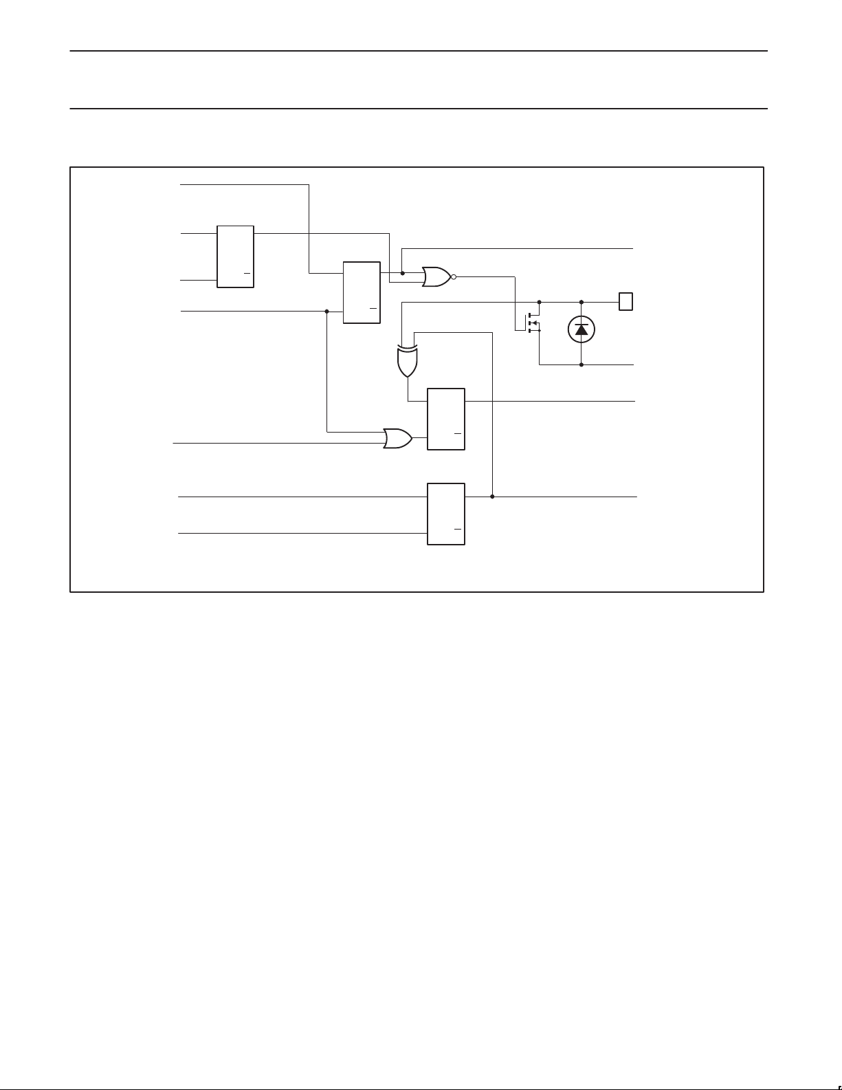
SIMPLIFIED SCHEMATIC OF I/O0
DATA FROM
SHIFT REGISTER
CONFIGURATION
DATA FROM
SHIFT REGISTER
WRITE
CONFIGURATION
PULSE
WRITE PULSE
READ PULSE
REGISTER
Q
D
FF
Q
C
K
D
Q
FF
Q
C
K
OUTPUT
PORT
REGISTER
INPUT PORT
REGISTER
D
Q
FF
Q
C
K
OUTPUT PORT
REGISTER DATA
I/O0
ESD PROTECTION DIODE
V
SS
INPUT PORT
REGISTER DATA
DATA FROM
SHIFT REGISTER
WRITE POLARITY
PULSE
NOTE: On power–up or reset, all registers return to default values.
Figure 4. Simplified schematic of I/O0
D
Q
FF
Q
C
K
POLARITY
INVERSION
REGISTER
POLARITY
REGISTER DATA
SW00795
2001 Dec 12
4
Page 5
Philips Semiconductors Product data
PCA95578-bit I2C and SMBus I/0 port with reset
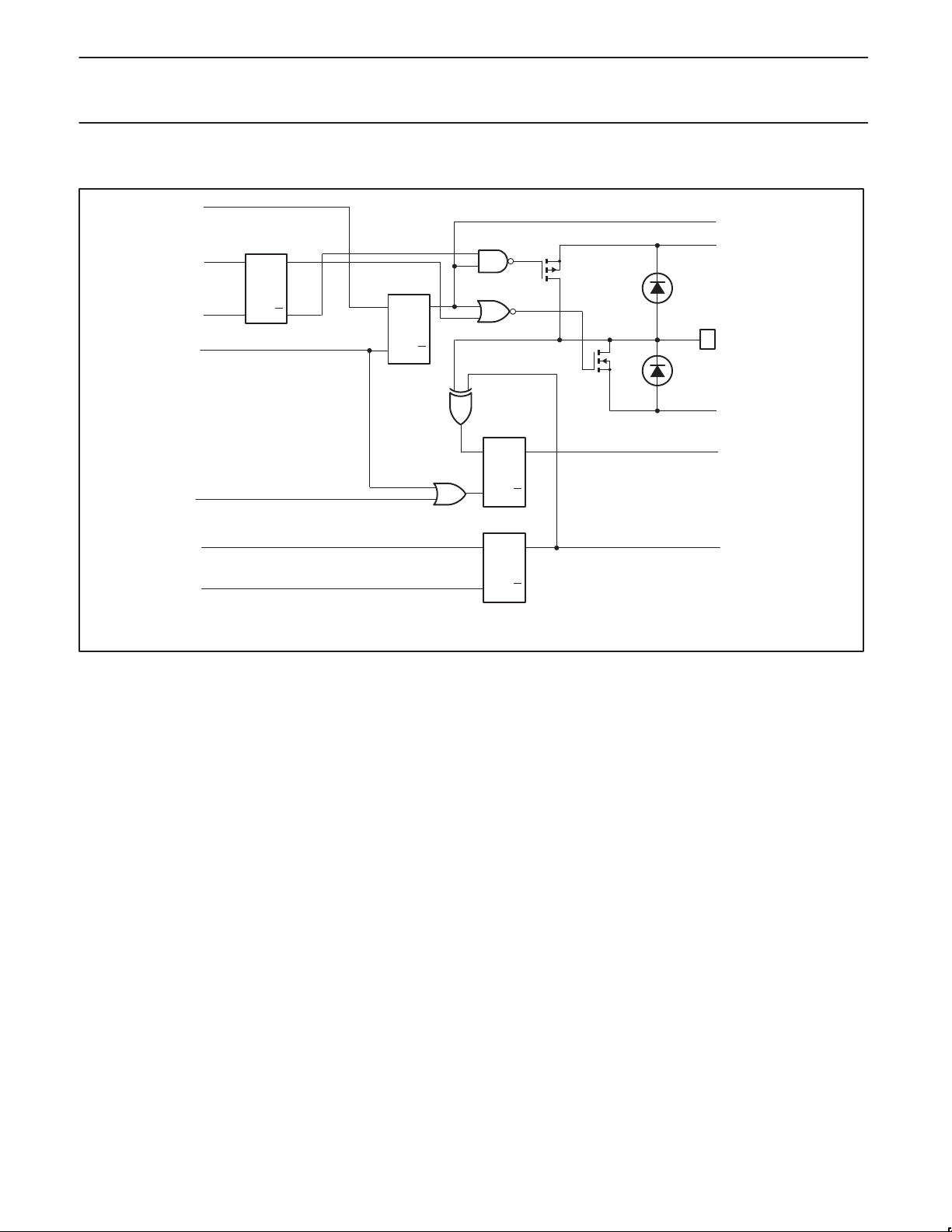
SIMPLIFIED SCHEMATIC OF I/O1 TO I/O7
DATA FROM
SHIFT REGISTER
CONFIGURATION
DATA FROM
SHIFT REGISTER
WRITE
CONFIGURATION
SHIFT REGISTER
WRITE POLARITY
PULSE
WRITE PULSE
READ PULSE
DATA FROM
PULSE
REGISTER
Q
D
FF
Q
C
K
D
Q
FF
Q
C
K
OUTPUT
PORT
REGISTER
NOTE: On power–up or reset, all registers return to default values.
Figure 5. Simplified schematic of I/O1 to I/O7
INPUT PORT
REGISTER
D
Q
FF
Q
C
K
D
Q
FF
Q
C
K
POLARITY
INVERSION
REGISTER
OUTPUT PORT
REGISTER DATA
V
DD
ESD PROTECTION DIODE
I/O1 TO I/O7
ESD PROTECTION DIODE
V
SS
INPUT PORT
REGISTER DATA
POLARITY
REGISTER DATA
SW00796
2001 Dec 12
5
Page 6

Philips Semiconductors Product data
PCA95578-bit I2C and SMBus I/0 port with reset
DEVICE ADDRESS
Following a START condition the bus master must output the
address of the slave it is accessing. The address of the PCA9557 is
shown in Figure 6. To conserve power, no internal pullup resistors
are incorporated on the hardware selectable address pins and they
must be pulled HIGH or LOW.
slave address
00 1 1A2A1A0
fixed programmable
R/W
su01048
Figure 6. PCA9557 address
The last bit of the slave address defines the operation to be
performed. When set to logic 1 a read is selected while a logic 0
selects a write operation.
CONTROL REGISTER
Following the successful acknowledgement of the slave address,
the bus master will send a byte to the PCA9557, which will be stored
in the control register. This register can be written and read via the
2
I
C bus.
0 0 0 0 D1 D00
0
Register 1 – Output Port Register
bit O7 O6 O5 O4 O3 O2 O1 O0
default
0 0 0 0 0 0 0 0
This register reflects the outgoing logic levels of the pins defined as
outputs by the Configuration Register. Bit values in this register have
no effect on pins defined as inputs. In turn, reads from this register
reflect the value that is in the flip-flop controlling the output selection,
NOT the actual pin value.
Register 2 – Polarity Inversion Register
bit N7 N6 N5 N4 N3 N2 N1 N0
default
1 1 1 1 0 0 0 0
This register enables polarity inversion of pins defined as inputs by
the Configuration Register. If a bit in this register is set (written
with ‘1’), the corresponding port pin’s polarity is inverted. If a bit in
this register is cleared (written with a ‘0’), the corresponding port
pin’s original polarity is retained.
Register 3 – Configuration Register
bit C7 C6 C5 C4 C3 C2 C1 C0
default
This register configures the directions of the I/O pins. If a bit in this
register is set, the corresponding port pin is enabled as an input with
high impedance output driver. If a bit in this register is cleared, the
corresponding port pin is enabled as an output.
1 1 1 1 1 1 1 1
SW00953
Figure 7. Control Register
REGISTER DEFINITION
D1 D0 NAME TYPE FUNCTION
0 0 Register 0 Read Input port register
0 1 Register 1 Read/Write Output port register
1 0 Register 2 Read/Write
1 1 Register 3 Read/Write
Polarity inversion
register
Configuration
register
REGISTER DESCRIPTION
Register 0 – Input Port Register
I7 I6 I5 I4 I3 I2 I1 I0
This register is an read-only port. It reflects the incoming logic levels
of the pins, regardless of whether the pin is defined as an input or an
output by the Configuration Register. Writes to this register have no
effect.
POWER-ON RESET
When power is applied to VDD, an internal power-on reset holds the
PCA9557 in a reset state until V
the reset condition is released and the PCA9557 registers and
2
I
C/SMBus state machine will initialize to their default states.
has reached V
DD
. At that point,
POR
For a power reset cycle, VDD must be set to 0 V, then ramped back
to the operating voltage.
RESET INPUT
A reset can be accomplished by holding the RESET pin LOW for a
minimum of t
machine will be held in their default state until the RESET
once again HIGH. This input typically requires a pull-up to V
. The PCA9557 registers and SMBus/I2C state
W
input is
CC.
2001 Dec 12
6
Page 7

Philips Semiconductors Product data
PCA95578-bit I2C and SMBus I/0 port with reset
CHARACTERISTICS OF THE I2C-BUS
The I2C-bus is for 2-way, 2-line communication between different ICs
or modules. The two lines are a serial data line (SDA) and a serial
clock line (SCL). Both lines must be connected to a positive supply
via a pull-up resistor when connected to the output stages of a device.
Data transfer may be initiated only when the bus is not busy.
Bit transfer
One data bit is transferred during each clock pulse. The data on the
SDA line must remain stable during the HIGH period of the clock
pulse as changes in the data line at this time will be interpreted as
control signals (see Figure 8).
SDA
SCL
data line
change
stable;
data valid
of data
allowed
Figure 8. Bit transfer
SDA
SW00363
Start and stop conditions
Both data and clock lines remain HIGH when the bus is not busy. A
HIGH-to-LOW transition of the data line, while the clock is HIGH is
defined as the start condition (S). A LOW-to-HIGH transition of the
data line while the clock is HIGH is defined as the stop condition (P)
(see Figure 9).
System configuration
A device generating a message is a ‘transmitter’, a device receiving
is the ‘receiver’. The device that controls the message is the
‘master’ and the devices which are controlled by the master are the
‘slaves’ (see Figure 10).
SDA
SDA
SCL
MASTER
TRANSMITTER/
RECEIVER
SCL
S P
START condition STOP condition
Figure 9. Definition of start and stop conditions
SLAVE
RECEIVER
SLAVE
TRANSMITTER/
RECEIVER
MASTER
TRANSMITTER
MASTER
TRANSMITTER/
RECEIVER
SLAVE
Figure 10. System configuration
SCL
SW00365
I2C
MULTIPLEXER
SW00366
2001 Dec 12
7
Page 8

Philips Semiconductors Product data
PCA95578-bit I2C and SMBus I/0 port with reset
Acknowledge
The number of data bytes transferred between the start and the stop conditions from transmitter to receiver is not limited. Each byte of eight bits
is followed by one acknowledge bit. The acknowledge bit is a HIGH level put on the bus by the transmitter whereas the master generates an
extra acknowledge related clock pulse.
A slave receiver which is addressed must generate an acknowledge after the reception of each byte. Also a master must generate an
acknowledge after the reception of each byte that has been clocked out of the slave transmitter. The device that acknowledges has to pull down
the SDA line during the acknowledge clock pulse, so that the SDA line is stable LOW during the HIGH period of the acknowledge related clock
pulse, set-up and hold times must be taken into account.
A master receiver must signal an end of data to the transmitter by not generating an acknowledge on the last byte that has been clocked out of
the slave. In this event, the transmitter must leave the data line HIGH to enable the master to generate a stop condition.
DATA OUTPUT
BY TRANSMITTER
DATA OUTPUT
BY RECEIVER
SCL FROM
MASTER
S
START condition
12
Figure 11. Acknowledgement on the I2C-bus
not acknowledge
acknowledge
89
clock pulse for
acknowledgement
SW00368
2001 Dec 12
8
Page 9

Philips Semiconductors Product data
PCA95578-bit I2C and SMBus I/0 port with reset
Bus Transactions
Data is transmitted to the PCA9557 registers using Write Byte transfers (see Figures 12 and 13). Data is read from the PCA9557 registers using
Read and Receive Byte transfers (see Figures 14 and 15).
12
SCL
345678
slave address data to port
9
command byte
SDA
WRITE TO
PORT
DATA OUT
FROM PORT
SCL
SDA
0 0 1 1 A2 A1 A0
S0A A A
start condition R/W
acknowledge
from slave
1000000 0
acknowledge
from slave
DATA 1
t
pv
P
acknowledge
from slave
DATA 1 VALID
SW00797
Figure 12. WRITE to output port register
12
345678
slave address data to register
0 0 1 1 A2 A1 A0
S0A A A
start condition R/W
9
command byte
0000001
acknowledge
from slave
1/0
acknowledge
from slave
DATA
P
acknowledge
from slave
SW00798
Figure 13. WRITE to I/O configuration or polarity inversion registers
acknowledge
slave address
S0A A A
1 A2 A1
from slave
A00 0
R/W
COMMAND BYTE
acknowledge
from slave
S
at this moment master-transmitter
becomes master-receiver and
slave-receiver becomes
slave-transmitter
1
1 A2 A1
acknowledge
from slave
A00 01
1
R/W
data from registerslave address
DATA
first byte
data from register
DATA
last byte
no acknowledge
from master
Figure 14. READ from register
2001 Dec 12
9
acknowledge
from master
A
PNA
su01052
Page 10

Philips Semiconductors Product data
PCA95578-bit I2C and SMBus I/0 port with reset
slave address data from port data from port
SDA
READ FROM
PORT
DATA INTO
PORT
00 1 1A2A1A0
S1A A
start condition R/W
t
ph
acknowledge
from slave
DATA 1 DATA 4
acknowledge
from master
DATA 3
t
ps
DATA 4DATA 2
no acknowledge
from master
NA
P
stop
condition
SW00799
NOTES:
1. This figure assumes the command byte has previously been programmed with 00h.
2. Transfer of data can be stopped at any moment by a stop condition. When this occurs, data present at the last acknowledge phase is valid
(output mode). Input data is lost.
Figure 15. READ input port register
TYPICAL APPLICATION
V
DD
V
DD
MASTER
CONTROLLER
GND
SCL
SDA
RESET
1.6 kΩ 1.6 kΩ 1.1 kΩ
2 kΩ
V
SCL
SDA
RESET
PCA9557
DD
I/0
0
I/0
1
I/0
2
I/0
3
I/0
4
2 kΩ
SUBSYSTEM 1
(e.g. temp sensor)
INT
RESET
SUBSYSTEM 2
(e.g. counter)
NOTE: Device address configured as 0011100 for this example
I/0
, I/01, I/02, configured as outputs
0
I/03, I/04, I/05, configured as inputs
I/006, I/07, are not used and have to be configured as outputs
2001 Dec 12
A2
A1
A0
Figure 16. Typical application
10
GND
I/0
5
I/0
6
I/0
7
ENABLE
A
Controlled Switch
(e.g. CBT device)
B
ALARM
SUBSYSTEM 3
(e.g. alarm
system)
SW00993
V
DD
Page 11

Philips Semiconductors Product data
I
DC input current on I/O0
PCA95578-bit I2C and SMBus I/0 port with reset
ABSOLUTE MAXIMUM RATINGS
In accordance with the Absolute Maximum Rating System (IEC 134).
SYMBOL
V
DD
V
I
I
I
I
IHL(max)
V
I/O
V
I/O0
I/O0
I
I/O
I
DD
I
SS
P
tot
T
stg
T
amb
DC supply voltage –0.5 +6 V
DC input voltage VSS – 0.5 5.5 V
DC input current — ± 20 mA
Maximum allowed input current through protection
diode (I/O1 – I/O7)
DC voltage on an I/O as an input other than I/O0 VSS – 0.5 5.5 V
DC voltage on I/O0 as an input VSS – 0.5 5.5 V
p
DC output current on an I/O — ± 50 mA
DC supply current — 85 mA
DC supply current — 100 mA
Total power dissipation — 200 mW
Storage temperature range –65 +150 °C
Operating ambient temperature –40 +85 °C
PARAMETER CONDITIONS MIN MAX UNIT
VI ≥ VDD or VI ≤ V
SS
— ±400 µA
— +400 µA
— –20 mA
HANDLING
Inputs and outputs are protected against electrostatic discharge in normal handling. However, to be totally safe, it is desirable to take
precautions appropriate to handling MOS devices. Advice can be found in Data Handbook IC24 under ”
Handling MOS devices
”.
2001 Dec 12
11
Page 12

Philips Semiconductors Product data
SYMBOL
PARAMETER
CONDITIONS
UNIT
HIGH level output current on I/O0
A
PCA95578-bit I2C and SMBus I/0 port with reset
DC CHARACTERISTICS
VDD = 2.3 to 5.5 V; VSS = 0 V; T
Supplies
V
V
I
DD
I
stbl
I
stbh
POR
DD
Supply voltage 2.3 — 5.5 V
Supply current
Standby current
Standby current
Power-on reset voltage
Input SCL; input/output SDA
V
V
IH
I
OL
I
L
C
LOW level input voltage –0.5 — 0.3 V
IL
HIGH level input voltage 0.7 V
LOW level output current VOL = 0.4 V 3 — — mA
Leakage current VI = VDD or V
Input capacitance VI = V
I
I/Os
V
V
IH
I
OL
LOW level input voltage –0.5 — 0.8 V
IL
HIGH level input voltage 2.0 — 5.5 V
LOW level output current VOL = 0.55 V; note 1 8 10 — mA
HIGH level output current except I/O0 VOH = 2.4 V; note 2 4 — — mA
I
OH
I
L
C
C
Input leakage current VDD = 5.5 V, VI = V
Input capacitance — 3.7 5 pF
I
Output capacitance — 3.7 5 pF
O
Select Inputs A0, A1, A2, and RESET
V
V
IH
I
LI
LOW level input voltage –0.5 — 0.8 V
IL
HIGH level input voltage 2.0 — 5.5 V
Input leakage current –1 — 1 µA
NOTES:
1. The total amount sunk by all I/Os must be limited to 100 mA and 25 mA per bit.
2. The total current sourced by all I/Os must be limited to 85 mA and 20 mA per bit.
= –40 to +85 °C; unless otherwise specified.
amb
Operating mode; VDD = 3.6 V; no load;
VI = VDD or VSS;
f
= 100 kHz
SCL
Standby mode; VDD = 5.5 V; no load;
VI = VSS; f
Standby mode; VDD = 5.5 V; no load;
VI = VDD; f
No load; Temp = 25 °C
VI = VDD or V
SS
p
VOH = 4.6 V — — 1
VOH = 3.3 V — — 1
= 0 kHz; I/O = inputs
SCL
= 0 kHz; I/O = inputs
SCL
SS
SS
SS
LIMITS
MIN TYP MAX
— — 1 µA
— — 1 µA
— — 1 µA
— 1.65 — V
DD
DD
— 5.5 V
–1 — +1 µA
— 6 10 pF
— — –100 µA
V
µ
2001 Dec 12
12
Page 13

Philips Semiconductors Product data
PCA95578-bit I2C and SMBus I/0 port with reset
AC SPECIFICA TIONS
SYMBOL P ARAMETER
f
SCL
t
BUF
t
HD;STA
t
SU;STA
t
SU;STO
t
HD;DAT
t
VD;ACK
t
VD;DAT
t
SU;DAT
t
LOW
t
HIGH
t
F
t
R
t
SP
Operating frequency 0 100 0 400 kHz
Bus free time between STOP and ST ART conditions 4.7 — 1.3 — µs
Hold time after (repeated) STAR T condition 4.0 — 0.6 — µs
Repeated START condition setup time 4.7 — 0.6 — µs
Setup time for STOP condition 4.0 — 0.6 — µs
Data in hold time 0 — 0 — ns
Valid time for ACK condition
Data out valid time
3
Data setup time 250 — 100 — ns
Clock LOW period 4.7 — 1.3 — µs
Clock HIGH period 4.0 — 0.6 — µs
Clock/Data fall time — 300 20 + 0.1 C
Clock/Data rise time — 1000 20 + 0.1 C
Pulse width of spikes that must be suppressed by the
input filters
Port Timing
t
PV
t
PV
t
PS
t
PH
Output data valid I/O0 — 250 — 250 ns
Output data valid I/O1 – I/O7 — 200 — 200 ns
Input data setup time 0 — 0 — ns
Input data hold time 200 — 200 — ns
Reset
t
W
t
REC
t
RESET
Reset pulse width 4 — 4 — ns
Reset recovery time 0 — 0 — ns
Time to reset 400 — 400 — ns
NOTES:
= total capacitance of one bus line in pF.
1. C
b
2. t
3. t
= time for Acknowledgement signal from SCL low to SDA (out) low.
VD;ACK
= minimum time for SDA data out to be valid following SCL low.
VD;DAT
STANDARD MODE
I2C BUS
MIN MAX MIN MAX
2
— 1 — 0.9 µs
— 1 — 0.9 µs
— 50 — 50 ns
FAST MODE
I2C BUS
1
b
1
b
UNITS
300 ns
300 ns
SDA
SCL
2001 Dec 12
t
BUF
t
LOW
t
HD;STA
t
R
t
HD;DAT
t
HIGH
t
F
t
SU;DAT
Sr
Figure 17. Definition of timing on the I2C-bus
13
t
HD;STA
t
SU;STA
t
SP
t
SU;STO
PP S
SU00645
Page 14

Philips Semiconductors Product data
PCA95578-bit I2C and SMBus I/0 port with reset
SO16: plastic small outline package; 16 leads; body width 3.9 mm SOT109-1
2001 Dec 12
14
Page 15

Philips Semiconductors Product data
PCA95578-bit I2C and SMBus I/0 port with reset
TSSOP16: plastic thin shrink small outline package; 16 leads; body width 4.4 mm SOT403-1
2001 Dec 12
15
Page 16

Philips Semiconductors Product data
PCA95578-bit I2C and SMBus I/0 port with reset
Purchase of Philips I2C components conveys a license under the Philips’ I2C patent
to use the components in the I2C system provided the system conforms to the
I2C specifications defined by Philips. This specification can be ordered using the
code 9398 393 40011.
Data sheet status
Product
Data sheet status
Objective data
Preliminary data
Product data
[1] Please consult the most recently issued data sheet before initiating or completing a design.
[2] The product status of the device(s) described in this data sheet may have changed since this data sheet was published. The latest information is available on the Internet at URL
http://www.semiconductors.philips.com.
[1]
status
Development
Qualification
Production
[2]
Definitions
Short-form specification — The data in a short-form specification is extracted from a full data sheet with the same type number and title. For
detailed information see the relevant data sheet or data handbook.
Limiting values definition — Limiting values given are in accordance with the Absolute Maximum Rating System (IEC 60134). Stress above one
or more of the limiting values may cause permanent damage to the device. These are stress ratings only and operation of the device at these or
at any other conditions above those given in the Characteristics sections of the specification is not implied. Exposure to limiting values for extended
periods may affect device reliability.
Application information — Applications that are described herein for any of these products are for illustrative purposes only. Philips
Semiconductors make no representation or warranty that such applications will be suitable for the specified use without further testing or
modification.
Disclaimers
Life support — These products are not designed for use in life support appliances, devices or systems where malfunction of these products can
reasonably be expected to result in personal injury . Philips Semiconductors customers using or selling these products for use in such applications
do so at their own risk and agree to fully indemnify Philips Semiconductors for any damages resulting from such application.
Right to make changes — Philips Semiconductors reserves the right to make changes, without notice, in the products, including circuits, standard
cells, and/or software, described or contained herein in order to improve design and/or performance. Philips Semiconductors assumes no
responsibility or liability for the use of any of these products, conveys no license or title under any patent, copyright, or mask work right to these
products, and makes no representations or warranties that these products are free from patent, copyright, or mask work right infringement, unless
otherwise specified.
Contact information
For additional information please visit
http://www.semiconductors.philips.com . Fax: +31 40 27 24825
For sales offices addresses send e-mail to:
sales.addresses@www.semiconductors.philips.com.
Definitions
This data sheet contains data from the objective specification for product development.
Philips Semiconductors reserves the right to change the specification in any manner without notice.
This data sheet contains data from the preliminary specification. Supplementary data will be
published at a later date. Philips Semiconductors reserves the right to change the specification
without notice, in order to improve the design and supply the best possible product.
This data sheet contains data from the product specification. Philips Semiconductors reserves the
right to make changes at any time in order to improve the design, manufacturing and supply.
Changes will be communicated according to the Customer Product/Process Change Notification
(CPCN) procedure SNW-SQ-650A.
Koninklijke Philips Electronics N.V. 2001
All rights reserved. Printed in U.S.A.
Date of release: 12-01
Document order number: 9397 750 09217
2001 Dec 12
16
 Loading...