

Page 1

INTEGRATED CIRCUITS
PCA9556
Octal SMBus Registered Interface
Product specification 1998 Dec 18
Page 2
Philips Semiconductors Product specification
PCA9556Octal SMBus Registered Interface
FEATURES
•SMBus compliance with fixed 3.3V voltage levels
•Operating power supply voltage range of 3.0V – 3.6V
•Active high polarity inverter register
•Write protect register
•Active low reset pin
•Low leakage current on power-down
•Noise filter on SCL/SDA inputs
•No glitch on power-up
•Internal power-on reset
•8 I/O pins which default to 8 inputs
•High impedance open drain on I/O
DESCRIPTION
The PCA9556 is a silicon CMOS circuit which provides parallel
input/output expansion for SMBus applications. The PCA9556
consists of an 8-bit input port register, 8-bit output port register, and
an SMBus interface. It has low current consumption and a high
impedance open drain output pin, I/O0.
The SMBus system master can reset the PCA9556 in the event of a
timeout by asserting a LOW on the reset input. The SMBus system
master can also invert the PCA9556 inputs by writing to their active
HIGH polarity inversion bits. Finally, the SMBus system master can
enable the PCA9556’s I/Os as either inputs or outputs by writing to
their I/O configuration bits.
The power-on reset sets the registers to their default values and
initializes the SMBus state machine. The RESET
same reset/initialization to occur without depowering the part.
pin causes the
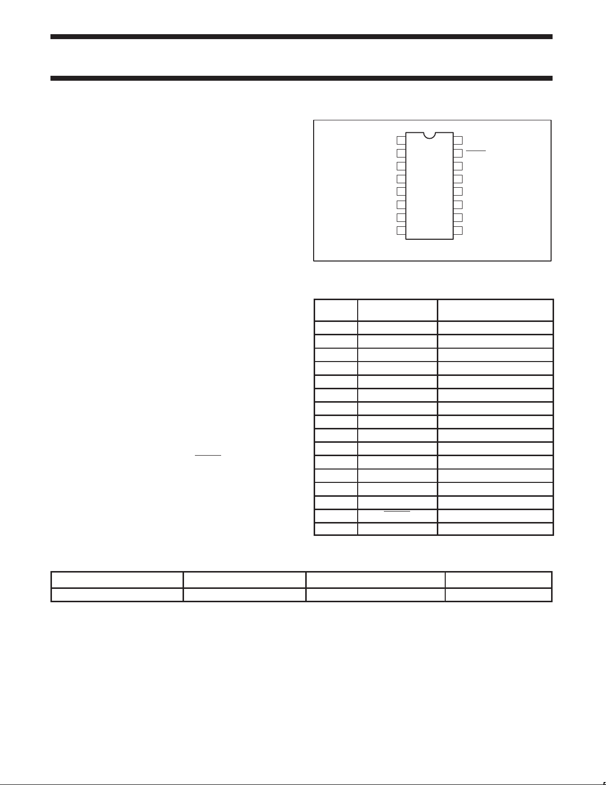
PIN CONFIGURATION
1
SCL
2
SDA
3
A0
A1
4
A2
5
6
I/O0
I/O1
7
V
8
SS
Figure 1. Pin configuration
16
15
14
13
12
11
10
9
su01045
V
DD
RESET
I/O7
I/O6
I/O5
I/O4
I/O3
I/O2
PIN DESCRIPTION
PIN
NUMBER
1 SCL Serial clock line
2 SDA Serial data line
3 A0 Address input 0
4 A1 Address input 1
5 A2 Address input 2
6 I/O0 I/O0 (open drain)
7 I/O1 I/O1
8 V
9 I/O2 I/O2
10 I/O3 I/O3
11 I/O4 I/O4
12 I/O5 I/O5
13 I/O6 I/O6
14 I/O7 I/O7
15 RESET External reset (active LOW)
16 V
SYMBOL FUNCTION
SS
DD
Supply GROUND
Supply voltage
ORDERING INFORMATION
PACKAGES TEMPERATURE RANGE OUTSIDE NORTH AMERICA DRAWING NUMBER
16-Pin Plastic TSSOP16 Type I 0°C to +70°C PCA9556 PW SOT403-1
1998 Dec 18 853-2138 20549
2
Page 3
Philips Semiconductors Product specification
PCA9556Octal SMBus Registered Interface
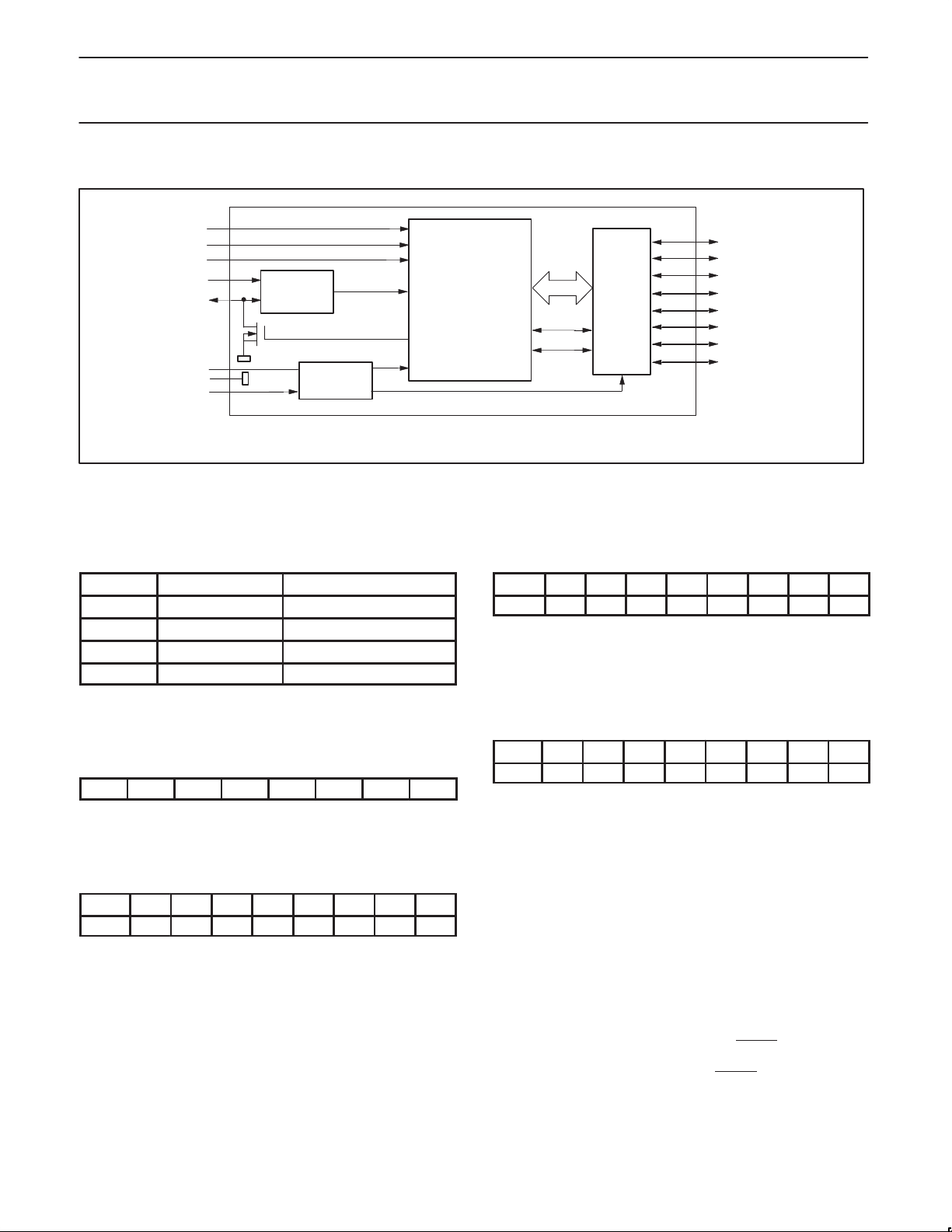
BLOCK DIAGRAM
A0
A1
A2
SCL
SDA
V
V
RESET
DD
SS
INPUT
FILTER
POWER-
ON
RESET
Figure 2. Block diagram
REGISTERS
Command Byte
Command Protocol Function
0 Read byte Input port register
1 Read/write byte Output port register
2 Read/write byte Polarity inversion register
3 Read/write byte I/O configuration register
The command byte is the first byte to follow the address byte during
a write transmission. It is used as a pointer to determine which of the
following registers will be written or read.
Register 0 – Input Port Register
I7 I6 I5 I4 I3 I2 I1 I0
This register is an input-only port. It reflects the incoming logic levels
of the pins, regardless of whether the pin is defined as an input or an
output by register 3. Writes to this register have no effect.
Register 1 – Output Port Register
O7 O6 O5 O4 O3 O2 O1 O0
bit
default 0 0 0 0 0 0 0 0
This register is an output-only port. It reflects the outgoing logic
levels of the pins defined as outputs by register 3. Bit values in this
register have no effect on pins defined as inputs. In turn, reads from
this register reflect the value that is in the flip-flop controlling the
output selection, NOT the actual pin value.
I/O0
I/O1
I/O2
I/O3
I/O4
I/O5
I/O6
I/O7
su01046
SMBUS
CONTROL
8-BIT
WRITE pulse
READ pulse
NOTE: ALL I/Os ARE SET TO INPUTS AT RESET
INPUT/
OUT-
PUT
PORTS
Register 2 – Polarity Inversion Register
bit N7 N6 N5 N4 N3 N2 N1 N0
default 1 1 1 1 0 0 0 0
This register enables polarity inversion of pins defined as inputs by
register 3. If a bit in this register is set (written with ‘1’), the
corresponding port pin’s polarity is inverted. If a bit in this register is
cleared (written with a ‘0’), the corresponding port pin’s original
polarity is retained.
Register 3 – Input/Output Configuration Register
bit C7 C6 C5 C4 C3 C2 C1 C0
default 1 1 1 1 1 1 1 1
This register configures the directions of the I/O pins. If a bit in this
register is set (written with ‘1’), the corresponding port pin is enabled
as an input with high impedance output driver. If a bit in this register
is cleared (written with ‘0’), the corresponding port pin is enabled as
an output.
RESET
Power-on Reset
When power is applied to VDD, an internal power-on reset holds the
PCA9556 in a reset state until V
has reached V
DD
the reset condition is released and the PCA9556 registers and
SMBus state machine will initialize to their default states.
External Reset
A reset can be accomplished by holding the RESET pin low for a
minimum of T
will be held in their default state until the RESET
high. This input contains an internal pull-up, therefore, it may be left
open if not used.
. The PCA9556 registers and SMBus state machine
W
input is once again
. At that point,
POR
1998 Dec 18
3
Page 4
Philips Semiconductors Product specification
PCA9556Octal SMBus Registered Interface
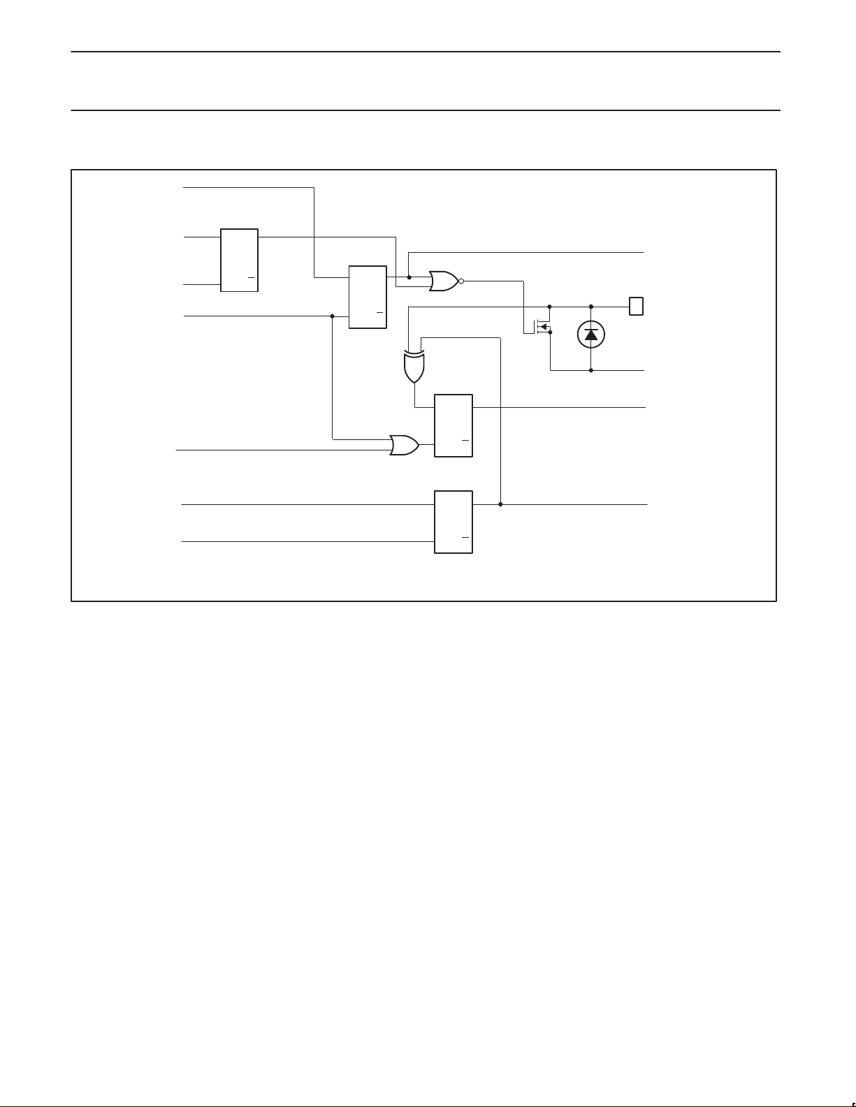
SIMPLIFIED SCHEMATIC OF I/O0
DATA FROM
SHIFT REGISTER
DATA FROM
SHIFT REGISTER
WRITE MASK PULSE
WRITE PULSE
READ PULSE
INPUT/OUTPUT
MASK REGISTER
Q
D
FF
Q
C
K
WRITE
REGISTER
D
Q
FF
Q
C
K
READ
REGISTER
D
Q
FF
Q
C
K
OUTPUT PORT
REGISTER DATA
I/O0
ESD PROTECTION DIODE
V
SS
INPUT PORT
REGISTER DATA
DATA FROM
SHIFT REGISTER
WRITE
POLARITY
PULSE
NOTE: ON POWER-UP OR RESET, ALL REGISTERS RETURN TO DEFAULT VALUES
Figure 3. Simplified schematic of I/O0
POLARITY
REGISTER
D
Q
FF
Q
C
K
POLARITY
REGISTER DATA
su01047
1998 Dec 18
4
Page 5

Philips Semiconductors Product specification
PCA9556Octal SMBus Registered Interface
SIMPLIFIED SCHEMATIC OF I/O1 TO I/O7
DATA FROM
SHIFT REGISTER
DATA FROM
SHIFT REGISTER
WRITE MASK PULSE
WRITE PULSE
READ PULSE
DATA FROM
SHIFT REGISTER
WRITE
POLARITY
PULSE
NOTE: ON POWER-UP OR RESET, ALL REGISTERS RETURN TO DEFAULT VALUES
INPUT/OUTPUT
MASK REGISTER
Q
D
FF
Q
C
K
WRITE
REGISTER
D
Q
FF
Q
C
K
Figure 4. Simplified schematic of I/O1 to I/O7
READ
REGISTER
D
Q
FF
Q
C
K
POLARITY
REGISTER
D
Q
FF
Q
C
K
OUTPUT PORT
REGISTER DATA
V
DD
ESD PROTECTION DIODE
I/O1 TO I/O7
ESD PROTECTION DIODE
V
SS
INPUT PORT
REGISTER DATA
POLARITY
REGISTER DATA
su01055
1998 Dec 18
5
Page 6

Philips Semiconductors Product specification
PCA9556Octal SMBus Registered Interface
SMBus Address
slave address
00 1 1A2A1A0
fixed programmable
R/W
su01048
Figure 5. PCA9556 address
SMBus Transactions
Data is transmitted to the PCA9556 registers using Write Byte transfers (see Figures 6 and 7). Data is read from the PCA9556 registers using
Read and Receive Byte transfers (see FIgures 8 and 9).
12
SCL
SDA
WRITE TO
PORT
DATA OUT
FROM PORT
345678
slave address data to port
0 0 1 1 A2 A1 A0
S0A A A
start condition R/W
9
acknowledge
from slave
command byte
1000000 0
acknowledge
from slave
DATA 1
t
pv
acknowledge
from slave
DATA 1 VALID
su01049
Figure 6. WRITE to output port register via Write Byte Protocol
12
SCL
SDA
S0A A A
start condition R/W
345678
slave address data to register
0 0 1 1 A2 A1 A0
9
command byte
0000001
acknowledge
from slave
1/0
acknowledge
from slave
DATA
acknowledge
from slave
su01050
Figure 7. WRITE to I/O configuration or polarity inversion registers via Write Byte Protocol
1998 Dec 18
6
Page 7

Philips Semiconductors Product specification
PCA9556Octal SMBus Registered Interface
acknowledge
slave address
S0A A A
1 A2 A1
from slave
A00 0
R/W
COMMAND BYTE
acknowledge
from slave
S
at this moment master-transmitter
becomes master-receiver and
slave-receiver becomes
slave-transmitter
1
1 A2 A1
acknowledge
from slave
A00 01
1
R/W
data from registerslave address
DATA
first byte
data from register
DATA
last byte
acknowledge
from master
no acknowledge
from master
Figure 8. READ from register via Read byte protocol
slave address data from port data from port
SDA
00 1 1A2A1A0
S1A A
start condition R/W
acknowledge
from slave
DATA 1 DATA 4
acknowledge
from master
no acknowledge
from master
NA
PNA
su01052
P
stop
condition
A
READ FROM
PORT
DATA INTO
PORT
DATA 3
t
ph
Notes:
1. This figure assumes the command byte has previously been programmed with 00h.
2. Transfer of data can be stopped at any moment by a stop condition. When this occurs,
data present at the last acknowledge phase is valid (output mode). Input data is lost.
t
ps
Figure 9. READ input port register via Receive byte protocol
DATA 4DATA 2
su01051
1998 Dec 18
7
Page 8

Philips Semiconductors Product specification
I
DC in ut current on I/O0
HIGH level out ut current on I/O0
µA
PCA9556Octal SMBus Registered Interface
ABSOLUTE MAXIMUM RATINGS
In accordance with the Absolute Maximum Rating System (IEC 134)
SYMBOL
V
T
V
V
I
I
P
P
T
DD
V
I
I/O
I/O0
I/O0
I
I/O
DD
SS
tot
stg
amb
I
O
Supply voltage –0.5 +4.6 V
Input voltage VSS – 0.5 VDD + 0.5 V
I
DC input current – ± 20 mA
DC voltage on an I/O as an input other than I/O0 VSS – 0.5 VDD + 0.5 V
DC voltage on I/O0 as an input VSS – 0.5 4.6 V
p
DC output current on an I/O – ± 20 mA
Supply current – mA
Supply current – mA
Total power dissipation – mW
Power dissipation per output – mW
Storage temperature range –65 +150 °C
Operating ambient temperature 0 +70 °C
HANDLING
Inputs and outputs are protected against electrostatic discharge in normal handling. However, to be totally safe, it is desirable to take
precautions appropriate to handling MOS devices. Advice can be found in Data Handbook IC24 under ”
PARAMETER CONDITIONS MIN MAX UNIT
– +400 µA
– –20 mA
Handling MOS devices
”.
DC CHARACTERISTICS
VDD = 3.0 to 3.6 V; VSS = 0 V; T
SYMBOL
Supplies
V
V
DD
I
DD
I
stb
POR
Supply voltage 3.0 3.6 V
Supply current
Standby current
Power-on reset voltage
input SCL; input/output SDA
V
V
I
OL
I
C
LOW level input voltage –0.5 0.8 V
IL
HIGH level input voltage 2.1 VDD + 0.5 V
IH
LOW level output current VOL = 0.4V 3 – mA
Leakage current VI = VDD = V
L
Input capacitance VI = V
I
I/Os
V
V
I
IHL(max)
I
OL
LOW level input voltage –0.5 – 0.8 V
IL
HIGH level input voltage 2.0 – VDD + 0.5 V
IH
Maximum allowed input current through
protection diode (I/O1 – I/O7)
LOW level output current VOL = 0.55V; VDD = 3.3V 8 10 – mA
HIGH level output current except I/O0 VOH = 2.4V; VDD = 3.3V 4 – mA
I
OH
I
C
C
Input leakage current V
L
Input capacitance – – 10 pF
I
Output capacitance – – 10 pF
O
Select Inputs A0, A1, A2, and RESET
V
V
I
LI
LOW level input voltage –0.5 0.8 V
IL
HIGH level input voltage 2.0 VDD + 0.5 V
IH
Input leakage current –1 1 µA
NOTE:
1. The power-on reset circuit resets the SMBus logic with V
= 0 to +70 °C; unless otherwise specified.
amb
PARAMETER CONDITIONS MIN TYP MAX UNIT
p
Operating mode; VDD = 3.3 V;
no load; VI = VDD or VSS;
= 100 kHz
f
SCL
Standby mode; VDD = 3.3 V
no load; VI = VDD or V
SS
VDD = 3.3 V
SS
SS;
no load; VI = VDD or V
SS
SS
VI ≥ VDD or VI ≤ V
note 1
–1 +1 µA
– 10 pF
– – ±400 µA
300 425 µA
25 50 µA
1.3 2.4 V
VDD = 3.6V; VOH = 4.6V – 1
VDD = 0V; VOH = 3.3V – 1
DD
= 3.6V; VI = 0 or V
DD
< V
and sets all I/Os to their default values
POR
DD
–1 1 µA
1998 Dec 18
8
Page 9

Philips Semiconductors Product specification
SYMBOL
PARAMETER
UNITS
PCA9556Octal SMBus Registered Interface
AC SPECIFICA TIONS
LIMITS
MIN MAX
F
SBM
T
BUF
T
HO:STA
T
SU:STA
T
HO:DAT
T
SU:DAT
T
LOW
T
HIGH
T
F
T
R
Port Timing
T
PV
T
PS
T
PH
Reset
T
W
Bus free time between stop and start conditions 4.7 µs
SMB operating frequency 10 100 KHz
Hold time after (repeated) start condition 4.0 µs
Repeated start condition setup time 4.7 µs
Data hold time 300 ns
Data setup time 250 ns
Clock LOW period 4.7 µs
Clock HIGH period 4.0 µs
Clock/Data fall time 300 ns
Clock/Data rise time 1000 ns
Output data valid 4 µs
Input data setup time 0 µs
Input data hold time 4 µs
Reset pulse width 2 ns
1998 Dec 18
9
Page 10

Philips Semiconductors Product specification
PCA9556Octal SMbus Registered Interface
TSSOP16: plastic thin shrink small outline package; 16 leads; body width 4.4 mm SOT403-1
1998 Dec 18
10
Page 11

Philips Semiconductors Product specification
PCA9556Octal SMbus Registered Interface
NOTES
1998 Dec 18
11
Page 12

Philips Semiconductors Product specification
PCA9556Octal SMbus Registered Interface
Purchase of Philips I2C components conveys a license under the Philips’ I2C patent
to use the components in the I2C system provided the system conforms to the
I2C specifications defined by Philips. This specification can be ordered using the
code 9398 393 40011.
Data sheet status
Data sheet
status
Objective
specification
Preliminary
specification
Product
specification
Product
status
Development
Qualification
Production
Definition
This data sheet contains the design target or goal specifications for product development.
Specification may change in any manner without notice.
This data sheet contains preliminary data, and supplementary data will be published at a later date.
Philips Semiconductors reserves the right to make chages at any time without notice in order to
improve design and supply the best possible product.
This data sheet contains final specifications. Philips Semiconductors reserves the right to make
changes at any time without notice in order to improve design and supply the best possible product.
[1]
[1] Please consult the most recently issued datasheet before initiating or completing a design.
Definitions
Short-form specification — The data in a short-form specification is extracted from a full data sheet with the same type number and title. For
detailed information see the relevant data sheet or data handbook.
Limiting values definition — Limiting values given are in accordance with the Absolute Maximum Rating System (IEC 134). Stress above one
or more of the limiting values may cause permanent damage to the device. These are stress ratings only and operation of the device at these or
at any other conditions above those given in the Characteristics sections of the specification is not implied. Exposure to limiting values for extended
periods may affect device reliability.
Application information — Applications that are described herein for any of these products are for illustrative purposes only. Philips
Semiconductors make no representation or warranty that such applications will be suitable for the specified use without further testing or
modification.
Disclaimers
Life support — These products are not designed for use in life support appliances, devices or systems where malfunction of these products can
reasonably be expected to result in personal injury . Philips Semiconductors customers using or selling these products for use in such applications
do so at their own risk and agree to fully indemnify Philips Semiconductors for any damages resulting from such application.
Right to make changes — Philips Semiconductors reserves the right to make changes, without notice, in the products, including circuits, standard
cells, and/or software, described or contained herein in order to improve design and/or performance. Philips Semiconductors assumes no
responsibility or liability for the use of any of these products, conveys no license or title under any patent, copyright, or mask work right to these
products, and makes no representations or warranties that these products are free from patent, copyright, or mask work right infringement, unless
otherwise specified.
Philips Semiconductors
811 East Arques Avenue
P.O. Box 3409
Sunnyvale, California 94088–3409
Telephone 800-234-7381
Copyright Philips Electronics North America Corporation 1999
All rights reserved. Printed in U.S.A.
Date of release: 04-99
Document order number: 9397 750 04974
1998 Dec 18
12
 Loading...