

Page 1
INTEGRATED CIRCUITS
PCA9544
2
4-channel I
C multiplexer and interrupt
controller
Product specification
Supersedes data of 1999 Apr 01
1999 Oct 07
Page 2
Philips Semiconductors Product specification
PCA95444-channel I2C multiplexer and interrupt controller
FEA TURES
•1-of-4 bi-directional translating multiplexer
•Channel selection via I
2
C bus
•Operating supply voltage 2.5 to 3.6 V
•Operating temperature range 0°C to 70°C
•Power-up with all multiplexer channels deselected
•3 address pins, allowing up to 8 devices on the I
2
C bus
•Low on resistance
DESCRIPTION
The PCA9544 is a 1-of-4 bi-directional translating multiplexer,
controlled via the I
four SCx/SDx downstream pairs, or channels. Only one SCx/SDx
channel is selected at a time, determined by the contents of the
programmable control register . Four interrupt inputs, one for each of
the SCx/SDx downstream pair, are provided. One interrupt output,
which acts as an AND of the four interrupt inputs, is provided. All I/O
pins are 5 V tolerant.
The pass gates of the multiplexer are constructed such that the V
pin can be used to limit the maximum high voltage which will be
passed by the PCA9544. This allows the use of different bus
voltages on each SCx/SDx pair, so that 3.3 V parts can
communicate with 5 V parts without any additional protection.
External pull-up resistors can pull the bus up to the desired voltage
level for this channel.
2
C bus. The SCL/SDA upstream pair fans out to
DD
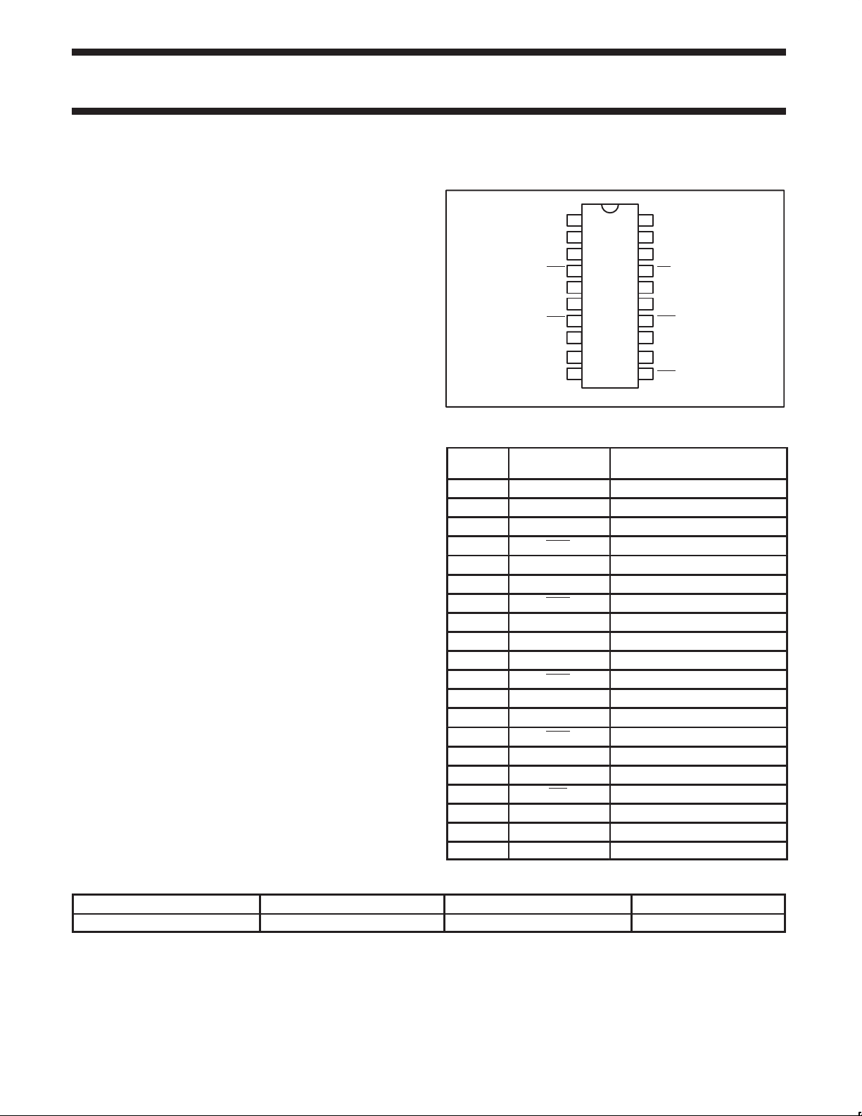
PIN CONFIGURATION
A0
1
2
A1
3
A2
4
INT0
5
SD0
6
SC0
INT1
7
8
SD1
SC1
9
10
VSS
PIN DESCRIPTION
PIN
NUMBER
1 A0 Address input 0
2 A1 Address input 1
3 A2 Address input 2
4 INT0 Interrupt input 0
5 SD0 Serial data 0
6 SC0 Serial clock 0
7 INT1 Interrupt input 1
8 SD1 Serial data 1
9 SC1 Serial clock 1
10 VSS Supply ground
11 INT2 Interrupt input 2
12 SD2 Serial data 2
13 SC2 Serial clock 2
14 INT3 Interrupt input 3
15 SD3 Serial data 3
16 SC3 Serial clock 3
17 INT Interrupt output
18 SCL Serial clock line
19 SDA Serial data line
20 V
SYMBOL FUNCTION
DD
Supply voltage
V
20
DD
SDA
19
SCL
18
INT
17
SC3
16
SD3
15
INT3
14
SC2
13
SD2
12
11
INT2
SW00373
ORDERING INFORMATION
PACKAGES TEMPERATURE RANGE ORDER CODE DRAWING NUMBER
20-Pin Plastic TSSOP 0°C to +70°C PCA9544 PW DH SOT360-1
1999 Oct 07 853–2178 22487
2
Page 3
Philips Semiconductors Product specification
PCA95444-channel I2C multiplexer and interrupt controller
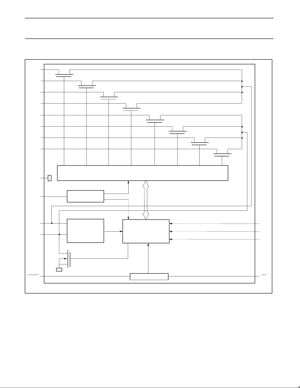
BLOCK DIAGRAM
SC0
SC1
SC2
SC3
SD0
SD1
SD2
SD3
V
SS
V
DD
SCL
SDA
INT[0–3] INT LOGIC INT
POWER-ON
RESET
INPUT
FILTER
2
I
C-BUS
CONTROL
SW00379
A0
A1
A2
1999 Oct 07
3
Page 4
Philips Semiconductors Product specification
PCA95444-channel I2C multiplexer and interrupt controller
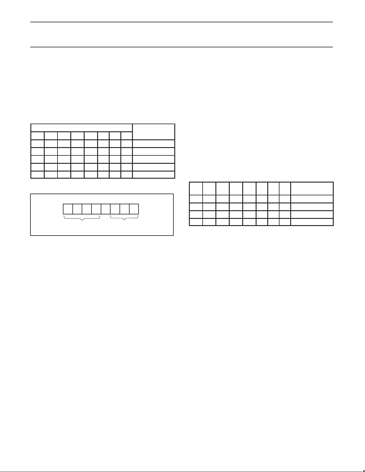
CHANNEL SELECTION
A SC0x/SD0x downstream pair, or channel, is selected by the
contents of the control register. This register is written after the
PCA9544 has been addressed. The 3 LSBs of the control byte are
used to determine which channel is to be selected. When a channel
is selected, the channel will become active after a stop condition has
been placed on the I
2
C bus. This ensures that all SCx/SDx lines will
be in a HIGH state when the channel is made active, so that no
false conditions are generated at the time of connection.
CONTROL BYTE
7 6 5 4 3 2 1 0
SELECTED
CHANNEL
X X X X X 0 X X none
X X X X X 1 0 0 0 (SC0/SD0)
X X X X X 1 0 1 1 (SC1/SD1)
X X X X X 1 1 0 2 (SC2/SD2)
X X X X X 1 1 1 3 (SC3/SD3)
CONTROL REGISTER
6 5 4 2 1 0 7 3
INT2 INT1 INT0 B2 B1 B0
INT3
Interrupt bits
(read only) (read/write)
X
Channel select bits
SW00386
INTERRUPT HANDLING
The PCA9544 provides 4 interrupt inputs, one for each channel and
one open drain interrupt output. When an interrupt is generated by any
device, it will be detected by the PCA9544 and the interrupt output
will be driven LOW. The channel need not be active for detection of
the interrupt. A bit is also set in the control byte. Bits 4 – 7 of the
control byte correspond to channels 0 – 3 of the PCA9544,
respectively. Therefore, if an interrupt is generated by any device
connected to channel 2, then bit 6 will be set in the control register.
Likewise, an interrupt on any device connected to channel 3 would
cause bit 7 of the control register to be set. The master can then
address the PCA 9544 and read the contents of the control byte to
determine which channel contains the device generating the interrupt.
The master can then reconfigure the PCA9544 to select this
channel, and locate the device generating the interrupt and clear it.
The interrupt clears when the device originating the interrupt clears.
It should be noted that more than one device can be providing an
interrupt on a channel, so it is up to the master to ensure that all
devices on a channel are interrogated for an interrupt.
7
6 5 4 3 2 1 0
0 0 0 1 X X X X 0 (SC0/SD0)
0 0 1 0 X X X X 1 (SC1/SD1)
0 1 0 0 X X X X 2 (SC2/SD2)
1 0 0 0 X X X X 3 (SC3/SD3)
INTERRUPTING
CHANNEL
POWER-ON RESET
During power-up, the control register defaults to all zeroes causing
all the channels to be deselected.
1999 Oct 07
4
Page 5

Philips Semiconductors Product specification
PCA95444-channel I2C multiplexer and interrupt controller
CHARACTERISTICS OF THE I2C-BUS
The I2C-bus is for 2-way, 2-line communication between different ICs
or modules. The two lines are a serial data line (SDA) and a serial
clock line (SCL). Both lines must be connected to a positive supply
via a pull-up resistor when connected to the output stages of a device.
Data transfer may be initiated only when the bus is not busy.
Bit transfer
One data bit is transferred during each clock pulse. The data on the
SDA line must remain stable during the HIGH period of the clock
pulse as changes in the data line at this time will be interpreted as
control signals (see FIgure 1).
SDA
SCL
data line
change
stable;
data valid
of data
allowed
Figure 1. Bit transfer
SDA
SW00363
Start and stop conditions
Both data and clock lines remain HIGH when the bus is not busy. A
HIGH-to-LOW transition of the data line, while the clock is HIGH is
defined as the start condition (S). A LOW-to-HIGH transition of the
data line while the clock is HIGH is defined as the stop condition (P)
(see Figure 2).
System configuration
A device generating a message is a ‘transmitter’, a device receiving
is the ‘receiver’. The device that controls the message is the
‘master’ and the devices which are controlled by the master are the
‘slaves’ (see Figure 3).
SDA
SDA
SCL
MASTER
TRANSMITTER/
RECEIVER
SCL
S P
START condition STOP condition
Figure 2. Definition of start and stop conditions
SLAVE
RECEIVER
SLAVE
TRANSMITTER/
RECEIVER
MASTER
TRANSMITTER
MASTER
TRANSMITTER/
RECEIVER
SLAVE
Figure 3. System configuration
SCL
SW00365
I2C
MULTIPLEXER
SW00366
1999 Oct 07
5
Page 6

Philips Semiconductors Product specification
PCA95444-channel I2C multiplexer and interrupt controller
Acknowledge
The number of data bytes transferred between the start and the stop conditions from transmitter to receiver is not limited. Each byte of eight bits
is followed by one acknowledge bit. The acknowledge bit is a HIGH level put on the bus by the transmitter whereas the master generates an
extra acknowledge related clock pulse.
A slave receiver which is addressed must generate an acknowledge after the reception of each byte. Also a master must generate an
acknowledge after the reception of each byte that has been clocked out of the slave transmitter. The device that acknowledges has to pull down
the SDA line during the acknowledge clock pulse, so that the SDA line is stable LOW during the HIGH period of the acknowledge related clock
pulse, set-up and hold times must be taken into account.
A master receiver must signal an end of data to the transmitter by not generating an acknowledge on the last byte that has been clocked out of
the slave. In this event, the transmitter must leave the data line HIGH to enable the master to generate a stop condition.
DATA OUTPUT
BY TRANSMITTER
DATA OUTPUT
BY RECEIVER
SCL FROM
MASTER
S
START condition
12
Figure 4. Acknowledgement on the I2C-bus
not acknowledge
acknowledge
89
clock pulse for
acknowledgement
SW00368
slave address
11
0A2A1 A0
1
hardware selectable
fixed
Figure 5. Slave address
SW00453
1999 Oct 07
6
Page 7

Philips Semiconductors Product specification
PCA95444-channel I2C multiplexer and interrupt controller
SDA
SCL
SDA
start condition R/W
XXXXXXXXXXXXXXXX
12
345 67 8
SLAVE ADDRESS
S0A
123456789
9
CONTROL REGISTER
acknowledge
from slave
PREVIOUS CHANNEL
Figure 6. WRITE control register
SLAVE ADDRESS
SDA
1 1 1 0 A2 A1 A0
S1A NA
start condition R/W acknowledge
CONTROL REGISTER
from slave
Figure 7. READ control register
INT0 P
acknowledge
from slave
A1 1 1 0 A2 A1 A0
B1INT1 B2INT2 XINT3
B0
t
pv
last byte
B0INT0 B1INT1 B2INT2 XINT3
no acknowledge
from master
NEW CHANNEL
SW00377
P
stop condition
SW00378
1999 Oct 07
7
Page 8

Philips Semiconductors Product specification
SYMBOL
PARAMETER
TEST CONDITIONS
UNIT
I
LOW level out ut current
mA
R
Switch resistance
Ω
V
Switch out ut voltage
V
PCA95444-channel I2C multiplexer and interrupt controller
ABSOLUTE MAXIMUM RATINGS
1, 2
In accordance with the Absolute Maximum Rating System (IEC 134).Voltages are referenced to GND (ground = 0 V).
SYMBOL
V
DD
V
I
I
I
I
O
I
DD
I
SS
P
tot
T
stg
T
amb
DC supply voltage –0.5 to +7.0 V
DC input voltage –0.5 to +7.0 V
DC input current ±20 mA
DC output current ±25 mA
Supply current ±100 mA
Supply current ±100 mA
total power dissipation 400 mW
Storage temperature range –60 to +150 °C
Operating ambient temperature 0 to +70 °C
PARAMETER CONDITIONS RATING UNIT
NOTES:
1. Stresses beyond those listed may cause permanent damage to the device. These are stress ratings only and functional operation of the
device at these or any other conditions beyond those indicated under “recommended operating conditions” is not implied. Exposure to
absolute-maximum-rated conditions for extended periods may affect device reliability .
2. The performance capability of a high-performance integrated circuit in conjunction with its thermal environment can create junction
temperatures which are detrimental to reliability. The maximum junction temperature of this integrated circuit should not exceed 150°C.
DC CHARACTERISTICS
VDD = 2.5 to 3.6 V; VSS = 0 V; T
Supply
VDDQn ≤ V
I
DD
I
stb
V
POR
Supply voltage 2.5 3.6 V
DD
Supply current
Standby current
Power-on reset voltage
Input SCL; input/output SDA
V
IL
V
IH
OL
I
L
C
i
LOW level input voltage –0.5 – 0.3 V
HIGH level input voltage 0.7 V
Leakage current VI = VDD or V
Input capacitance VI = V
Select inputs A0 to A2 / INT0 to INT3
V
IL
V
IH
I
LI
LOW level input voltage –0.5 – +0.3 V
HIGH level input voltage 0.7 V
Input leakage current pin at VDD or V
Pass Gate
ON
Pass
I
L
Leakage current VI = VDD or V
INT Output
I
OL
I
L
LOW level output current VOL = 0.4 V 3 – – mA
Leakage current VI = VDD or V
= 0°C to +70°C; unless otherwise specified.
amb
Operating mode; VDD = 3.6 V;
no load; VI = VDD or VSS;
Standby mode; VDD = 3.6 V;
no load; VI = VDD or V
VDD = 3.6 V; no load;
VI = VDD or V
p
VCC = 3.67 V, VO = 0.4 V, IO = 15 mA 5 20 30
VCC = 2.3 to 2.7 V, VO = 0.4V, IO = 10 mA 7 26 55
V
= VDD = 3.3 V; I
swin
V
= VDD = 3.0 to 3.6 V; I
p
swin
V
= VDD = 2.5 V; I
swin
V
= VDD = 2.3 to 2.7 V; I
swin
LIMITS
MIN TYP MAX
– 20 100 µA
f
= 100 kHz
SCL
SS
SS
– 2.5 100 µA
– 1.3 2.1 V
DD
– 6 V
VOL = 0.4 V 3 – –
VOL = 0.6 V 6 – –
SS
SS
SS
= –100 µA 2.2
swout
= –100 µA 1.6 2.8
swout
= –100 µA 1.5
swout
= –100 µA 1.1 2.0
swout
SS
SS
–1 – +1 µA
– – 13 pF
DD
– VDD + 0.5 V
–1 – +1 µA
–1 – +1 µA
–1 – +1 µA
DD
DD
V
V
1999 Oct 07
8
Page 9

Philips Semiconductors Product specification
PCA95444-channel I2C multiplexer and interrupt controller
AC CHARACTERISTICS
STANDARD-MODE
SYMBOL PARAMETER
I2C-BUS
MIN MAX MIN MAX
t
pd
f
SCL
t
BUF
t
HD:STA
t
LOW
t
HIGH
t
SU:STA
Propagation delay from SDA to SDn or SCL to SC
n
0.3
SCL clock frequency 0 100 0 400 KHz
Bus free time between a STOP and ST ART condition 4.7 – 1.3 – µs
Hold time (repeated) STAR T condition
After this period, the first clock pulse is generated
4.0 – 0.6 – µs
LOW period of the SCL clock 4.7 – 1.3 – µs
HIGH period of the SCL clock 4.0 – 0.6 – µs
Set-up time for a repeated STAR T condition 4.7 – 0.6 µs
Data hold time:
t
HD:DAT
t
SU:DAT
t
SU:STO
t
t
C
r
f
b
for CBUS compatible masters 5.0 – – – µs
for I2C-bus devices 0
2
– 0
Data set-up time 250 – 100
Set-up time for STOP condition – 1000 – 300 ns
Rise time of both SDA and SCL signals – 300 – 300 ns
Fall time of both SDA and SCL signals 4.0 – 0.6 – µs
Capacitive load for each bus line 400 – 400 pF
INT
t
iv
t
ir
L
pwr
H
pwr
INTn to INT active valid time 4 4 µs
INTn to INT inactive delay time 2 2 µs
LOW level pulse width rejection or INTn inputs 1 1 ns
HIGH level pulse width rejection or INTn inputs 500 500 ns
NOTES:
1. Pass gate propagation delay is calculated from the 20Ω typical R
2. A device must internally provide a hold time of at least 300ns for the SDA signal (referred to the VIH
and and the 15pF load capacitance.
ON
the undefined region of the falling edge of SCL.
3. The maximum t
4. A fast-mode I
2
has only to be met if the device does not stretch the LOW period (t
HD:DAT
C bus device can be used in a standard-mode I2C-bus system, but the requirement t
LOW
will automatically be the case if the device does not stretch the LOW period of the SCL signal. If such a device does stretch the LOW period
of the SCL signal, it must output the next data bit to the SDA line t
2
C-bus specification) before the SCL line is released.
I
5. C
= total capacitance of one bus line in pF.
b
rmax
+ t
= 1000 + 250 = 1250ns (according to the standard-mode
SU:DAT
FAST-MODE I2C-BUS
1
2
4
of the SCL signal) in order to bridge
min
) of the SCL signal.
≥ 250ns must then be met. This
SU:DAT
1
0.3
3
0.9
– ns
UNIT
ns
µs
SDA
SCL
1999 Oct 07
t
BUF
t
LOW
t
HD;STA
t
R
t
HD;DAT
t
HIGH
t
F
t
SU;DAT
Sr
Figure 8. Definition of timing on the I2C-bus
9
t
t
SU;STA
HD;STA
t
SP
t
SU;STO
PP S
SU00645
Page 10

Philips Semiconductors Product specification
PCA95444-channel I2C multiplexer and interrupt controller
TSSOP20: plastic thin shrink small outline package; 20 leads; body width 4.4 mm SOT360-1
1999 Oct 07
10
Page 11

Philips Semiconductors Product specification
PCA95444-channel I2C multiplexer and interrupt controller
NOTES
1999 Oct 07
11
Page 12

Philips Semiconductors Product specification
PCA95444-channel I2C multiplexer and interrupt controller
Purchase of Philips I2C components conveys a license under the Philips’ I2C patent
to use the components in the I2C system provided the system conforms to the
I2C specifications defined by Philips. This specification can be ordered using the
code 9398 393 40011.
Data sheet status
Data sheet
status
Objective
specification
Preliminary
specification
Product
specification
Product
status
Development
Qualification
Production
Definition
This data sheet contains the design target or goal specifications for product development.
Specification may change in any manner without notice.
This data sheet contains preliminary data, and supplementary data will be published at a later date.
Philips Semiconductors reserves the right to make changes at any time without notice in order to
improve design and supply the best possible product.
This data sheet contains final specifications. Philips Semiconductors reserves the right to make
changes at any time without notice in order to improve design and supply the best possible product.
[1]
[1] Please consult the most recently issued datasheet before initiating or completing a design.
Definitions
Short-form specification — The data in a short-form specification is extracted from a full data sheet with the same type number and title. For
detailed information see the relevant data sheet or data handbook.
Limiting values definition — Limiting values given are in accordance with the Absolute Maximum Rating System (IEC 134). Stress above one
or more of the limiting values may cause permanent damage to the device. These are stress ratings only and operation of the device at these or
at any other conditions above those given in the Characteristics sections of the specification is not implied. Exposure to limiting values for extended
periods may affect device reliability.
Application information — Applications that are described herein for any of these products are for illustrative purposes only. Philips
Semiconductors make no representation or warranty that such applications will be suitable for the specified use without further testing or
modification.
Disclaimers
Life support — These products are not designed for use in life support appliances, devices or systems where malfunction of these products can
reasonably be expected to result in personal injury . Philips Semiconductors customers using or selling these products for use in such applications
do so at their own risk and agree to fully indemnify Philips Semiconductors for any damages resulting from such application.
Right to make changes — Philips Semiconductors reserves the right to make changes, without notice, in the products, including circuits, standard
cells, and/or software, described or contained herein in order to improve design and/or performance. Philips Semiconductors assumes no
responsibility or liability for the use of any of these products, conveys no license or title under any patent, copyright, or mask work right to these
products, and makes no representations or warranties that these products are free from patent, copyright, or mask work right infringement, unless
otherwise specified.
Philips Semiconductors
811 East Arques Avenue
P.O. Box 3409
Sunnyvale, California 94088–3409
Telephone 800-234-7381
Copyright Philips Electronics North America Corporation 1999
All rights reserved. Printed in U.S.A.
Date of release: 10-99
Document order number: 9397–750–06498
1999 Oct 07
12
 Loading...