

Page 1

INTEGRATED CIRCUITS
PCA8550
2
4-bit multiplexed/1-bit latched 5-bit I
C
EEPROM
Product specification 1998 Sep 29
Page 2
Philips Semiconductors Product specification
PCA85504-bit multiplexed/1-bit latched 5-bit I2C EEPROM
FEA TURES
•4-bit 2-to-1 multiplexer, 1-bit latch
•5-bit internal non-volatile register
•Override input forces all outputs to logic 0
•Internal non-volatile register write/readable via I
•Write-protect pin enables/disables I
2
C writes to register
2
C bus
•2.5V multiplexed outputs
•3.3V non-multiplexed output (latched)
•5V tolerant inputs
•Useful for ’jumperless’ configuration of PC motherboards
•Designed for use in Pentium Pro/Pentium II systems
Pentium II is a registered trademark of Intel Corporation
DESCRIPTION
The primary function of the 4-bit 2-to-1 I2C multiplexer is to select
either a 4-bit input or data from a non-volatile register and drive this
value onto the output pins. One additional non-multiplexed register
output is also provided. The non-multiplexed output is latched to
prevent output value changes during I
register. A write protect input is provided to enable/disable the ability
to write to the non-volatile register. An ‘‘override” input feature forces
all outputs to logic 0.
2
C writes to the non-volatile
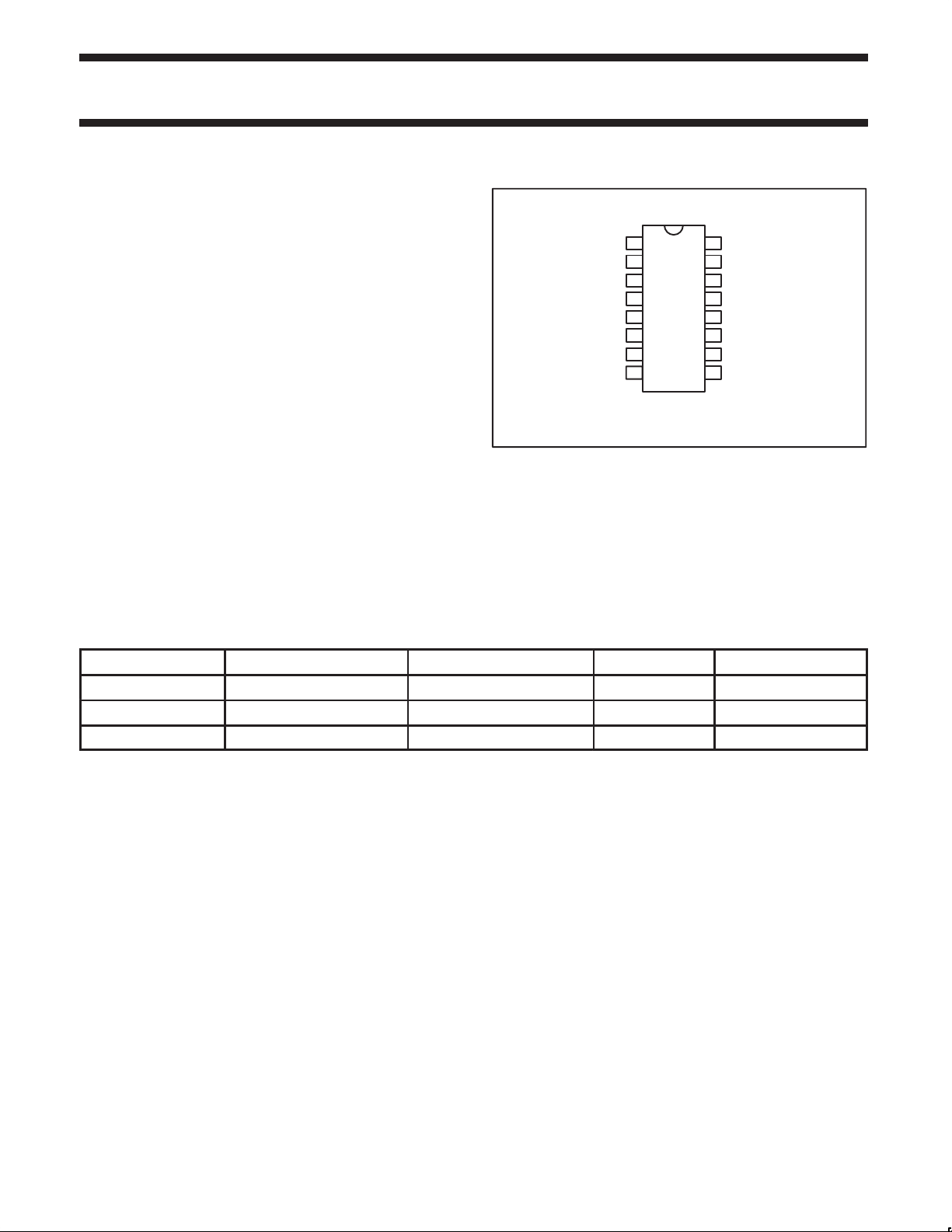
PIN CONFIGURATION
2
C SCL
1
I
2
2
C SDA
I
GND
3
4
5
6
7
8
OVERRIDE#
MUX_IN A
MUX_IN B
MUX_IN C
MUX_IN D
SW00216
V
16
CC
WP
15
NON_MUXED_OUT
14
MUX_SELECT
13
MUX_OUT A
12
11
MUX_OUT B
MUX_OUT C
10
MUX_OUT D
9
ORDERING INFORMATION
PACKAGES TEMPERATURE RANGE OUTSIDE NORTH AMERICA NORTH AMERICA DRAWING NUMBER
16-Pin Plastic SO 0°C to +70°C PCA8550D PCA8550D SOT109-1
16-Pin Plastic SSOP 0°C to +70°C PCA8550DB PCA8550DB SOT338-1
16-Pin Plastic TSSOP 0°C to +70°C PCA8550PW PCA8550PW DH SOT403-1
FUNCTIONAL DESCRIPTION
When the MUX_SELECT signal is logic 0, the multiplexer will select
the data from the non-volatile register to drive on the MUX_OUT
pins. When the MUX_SELECT signal is logic 1, the multiplexer will
select the MUX_IN lines to drive on the MUX_OUT pins. The
MUX_SELECT signal is also used to latch the NON_MUXED_OUT
signal which outputs data from the non-volatile register. The
NON_MUXED_OUT signal latch is transparent when MUX_SELECT
is in a logic 0 state, and will latch data when MUX_SELECT is in a
logic 1 state. When the active-LOW OVERRIDE# signal is set to
logic 0 and the MUX_SELECT signal is at a logic 0, all outputs will
be driven to logic 0. This information is summarized in Table 1.
The write protect (WP) input is used to control the ability to write the
contents of the 5-bit non-volatile register. If the WP signal is logic 0,
2
the I
C bus will be able to write the contents of the non-volatile
register. If the WP signal is logic 1, data will not be allowed to be
written into the non-volatile register.
The factory default for the contents of the non-volatile register are all
logic 0. These stored values can be read or written using the I
bus (described in the next section).
The OVERRIDE#, WP, MUX_IN, and MUX_SELECT signals have
internal pullup resistors. See the DC and AC Characteristics for
hysteresis and signal spike suppression figures.
2
C
1998 Sep 29 853-2015 20105
2
Page 3
Philips Semiconductors Product specification
External in uts to multi lexer
2.5V multi lexed out ut
PCA85504-bit multiplexed/1-bit latched 5-bit I2C EEPROM
PIN DESCRIPTION
PIN
NUMBER
1 I2C SCL I2C bus clock
2 I2C SDA Bi-directional I2C bus data
3 OVERRIDE# Forces all outputs to logic 0
4 MUX_IN A
5 MUX_IN B
6 MUX_IN C
7 MUX_IN D
8 GND Common ground voltage rail
9 MUX_OUT D
10 MUX_OUT C
11 MUX_OUT B
12 MUX_OUT A
13 MUX_SELECT
14 NON_MUXED_OUT
15 WP
16 V
SYMBOL FUNCTION
p
p
Selects MUX_IN inputs or
register contents for
MUX_OUT outputs
TTL-level output from
non-volatile memory
Non-volatile register
write-protect
CC
Positive voltage rail
FUNCTION TABLE
Table 1. Function table
OVERRIDE
#
MUX_SELECT
0 0 All 0’ s All 0’s
0 1
p
1 0
1 1
NOTE
1. Latched NON_MIXED_OUT state will be the value present on
the NON_MUXED_OUT output at the time of the MUX_SELECT
p
input transitioned from a logic 0 to a logic 1 state.
MUX_OUT
OUTPUTS
MUX_IN
inputs
From non-
volatile
register
MUX_IN
inputs
NON_MUXED_OUT
OUTPUT
Latched
NON_MUXED_OUT
From non-volatile
register
From non-volatile
register
1
2
C Interface
I
Communicating with this device is initiated by sending a valid address on the I2C bus. The address format (see FIgure 1) is a fixed unique 7-bit
value followed by a 1-bit read/write value which determines the direction of the data transfer.
MSB LSB
10 0
11 1 0
R/W#
SW00218
Figure 1. I2C Address Byte
Following the address and acknowledge bit are 8 data bits which, depending on the read/write bit in the address, will read data from or write
data to the non-volatile register . Data will be written to the register if the read/write bit is logic 0 and the WP input is logic 0. Data will be read
from the register if the bit is logic 1. The three high-order bits (see FIgure 2) are logic 0. The next bit is data which is non-multiplexed. The low
four bits are the data which will be multiplexed. A write with any of the first three bits non-zero will be aborted.
NOTE:
1. To ensure data integrity, the non-volatile register must be internally write protected when V
component is dropped below normal operating levels.
to the I2C bus is powered down or VCC to the
CC
1998 Sep 29
3
Page 4
Philips Semiconductors Product specification
PCA85504-bit multiplexed/1-bit latched 5-bit I2C EEPROM
MSB LSB
0
BLOCK DIAGRAM
CRESET#
13
MUX_SELECT
OVERRIDE#
3
= 16
V
CC3.3
GND = 8
SCL
1
2
I
C CLOCK
CHIP
SET
2
15
4
5
6
7
SDA
2
C DATA
I
WRITE
PROTECT
A20M#
MUX_IN A
IGNNE#
MUX_IN B
LINT0/INTR
MUX_IN C
LINT1/NMI
MUX_IN D
00
10–30k Ω
100–150k Ω
10–30k Ω
10–30k Ω
I C iNTERFACE LOGIC
2
OE#
NON-
MUXED
DATA
Figure 2. I2C Data Byte
5-BIT EEPROM
MUX
DATA D
MUX
DATA C
LATCH
NMO
0
3.3V
4-BIT 2-to-1 MULTIPLEXER
3.3V
3.3V
3.3V
1
MUX
DATA B
SELECT
NON_MUX_OUT
A20M#
2.5V
MUX_OUT A
/FSBM0
2.5V
IGNNE#
MUX_OUT B
/FSBM1
LINT0/INTR
2.5V
MUX_OUT C
/FSBM2
2.5V
LINT1/NMI
MUX_OUT D
/FSBM3
MUX
DATA A
SW00219
14
12
11
10
9
PENTIUM PRO/
PENTIUM II
PROCESSORS
1998 Sep 29
SW00347
4
Page 5

Philips Semiconductors Product specification
SYMBOL
PARAMETER
CONDITIONS
UNIT
PCA85504-bit multiplexed/1-bit latched 5-bit I2C EEPROM
ABSOLUTE MAXIMUM RATINGS
1, 2
In accordance with the Absolute Maximum Rating System (IEC 134)
Voltages are referenced to GND (ground = 0V)
SYMBOL
V
CC
V
I
V
OUT
T
stg
DC supply voltage –0.5 to +4.6 V
DC input voltage Note 3 –1.5 to VCC +1.5 V
DC output voltage Note 3 –0.5 to VCC +0.5 V
Storage temperature range –60 to +150 °C
PARAMETER CONDITIONS RATING UNIT
NOTES:
1. Stresses beyond those listed may cause permanent damage to the device. These are stress ratings only and functional operation of the
device at these or any other conditions beyond those indicated under “recommended operating conditions” is not implied. Exposure to
absolute-maximum-rated conditions for extended periods may affect device reliability .
2. The performance capability of a high-performance integrated circuit in conjunction with its thermal environment can create junction
temperatures which are detrimental to reliability. The maximum junction temperature of this integrated circuit should not exceed 150°C.
3. The input and output voltage ratings may be exceeded if the input and output current ratings are observed.
RECOMMENDED OPERATING CONDITIONS
LIMITS
MIN MAX
V
CC
SCL, SDA
OVERRIDE#,
MUX_IN,
MUX_SELECT
MUX_OUT,
NON_MUXED_OUT
dt/dv Input transition rise or fall time 0 10 ns/V
T
A
DC supply voltage 3.0 3.6 V
V
IL
V
IH
V
OL
V
IL
V
IH
I
OL
I
OH
IOL= 3mA
–0.5
2.7
–0.5
2.0
0.9
4.0
0.4
0.8
4.0
2.0
–2.0
mA
Operating temperature 0 70 °C
V
V
1998 Sep 29
5
Page 6

Philips Semiconductors Product specification
PCA85504-bit multiplexed/1-bit latched 5-bit I2C EEPROM
DC CHARACTERISTICS
LIMITS
SYMBOL PARAMETER
SCL, SDA
OVERRIDE#, WP,
MUX_SELECT
MUX A ⇒ D
MUX_OUT
NON_MUXED_OUT
I
CC
I
CC
C
IN
NOTES:
1. V
2. Human body model
is the hysteresis of Schmitt-Trigger inputs
HYS
V
OL
IOL (VOL = 0.4V)
IOL (VOL = 0.6V)
IIL (VIL = 0.4V)
I
(VIH = 2.4V)
IH
V
HYS
I
IL
I
IH
1
IIL (VIL = 0.4V)
IIH (VIH = 2.4V)
VOL (IOL = 100µA)
VOL (IOL = 2.0mA)
VOH (IOH = –100µA)
VOH (IOH = –1.0mA)
VOL (IOL = 100µA)
VOL (IOL = 2.0mA)
VOH (IOH = –100µA)
VOH (IOH = –2.0mA)
CC
CC =
3.3V)
Quiescent supply current (V
VI = 0V to V
Quiescent supply current
VI = V
CC
All inputs 10 pF
ESD protection 2.0 KV
Input diode clamp voltage –1.5 V
Temp = 0°C to +70°C
3.0V < VCC ≤ 3.6V
MIN MAX
0
0.6
3.0
6.0
–7
–1.5
–32
–12
0.19
–86
–20
–0.72
–0.166
–0.3
–0.3
2.0
1.7
–0.5
–0.5
2.4
2.0
–267
–100
–2.0
–0.75
0.4
0.7
2.625
2.625
0.4
0.7
3.6
3.6
500 µA
UNIT
V
mA
mA
µA
µA
V
µA
mA
V
V
10 mA
NON-VOLATILE STORAGE SPECIFICATIONS
Parameter Specification
Memory cell data retention 10 years min
Number of memory cell write cycles 1,000 cycles min
1998 Sep 29
6
Page 7

Philips Semiconductors Product specification
PCA85504-bit multiplexed/1-bit latched 5-bit I2C EEPROM
AC CHARACTERISTICS
LIMITS
SYMBOL PARAMETER MIN MAX UNIT
T
MPD
T
SOV
T
OVN
T
OVM
T
R
T
F
C
L
f
SCL
T
SCH
T
SCL
T
DSP
T
SDS
T
SDH
T
ICR
T
ICF
T
BUF
T
STS
T
STH
T
SPS
C
B
T
W
NOTE:
1. WRITE CYCLE time can only be measured indirectly during write cycle. The device will not acknowledge its I
Mux input to output propagation delay 20.0 ns
MUX_SELECT to output valid 22 ns
OVERRIDE# to NON_MUX output delay 15.0 ns
OVERRIDE# to mux output delay 25.0 ns
Output rise time 1.0 3.0 ns/V
Output fall time 1.0 3.0 ns/V
Test load capacitance on Muxed/Non-Muxed
outputs
15 pF
I2C BUS
I2C clock frequency 10 400 KHz
I2C clock high time 600 ns
I2C clock low time 1.3 ns
I2C data spike time 0 50 ns
I2C data setup time 100 ns
I2C data hold time 0 ns
I2C input rise time (10–400pF bus) 20 300 ns
I2C input fall time (10–400pF bus) 20 300 ns
I2C bus free time between start and stop 1.3 ns
I2C repeated start condition setup 600 ns
I2C repeated start condition hold 600 ns
I2C stop condition setup 600 ns
I2C bus capacitive load 400 pF
Write cycle time
1
TYPICAL = 15 ms
2
C address.
1998 Sep 29
7
Page 8

Philips Semiconductors Product specification
PCA85504-bit multiplexed/1-bit latched 5-bit I2C EEPROM
SO16: plastic small outline package; 16 leads; body width 3.9 mm SOT109-1
1998 Sep 29
8
Page 9

Philips Semiconductors Product specification
PCA85504-bit multiplexed/1-bit latched 5-bit I2C EEPROM
SSOP16: plastic shrink small outline package; 16 leads; body width 5.3 mm SOT338-1
1998 Sep 29
9
Page 10

Philips Semiconductors Product specification
PCA85504-bit multiplexed/1-bit latched 5-bit I2C EEPROM
TSSOP16: plastic thin shrink small outline package; 16 leads; body width 4.4 mm SOT403-1
1998 Sep 29
10
Page 11

Philips Semiconductors Product specification
PCA85504-bit multiplexed/1-bit latched 5-bit I2C EEPROM
NOTES
1998 Sep 29
11
Page 12

Philips Semiconductors Product specification
PCA85504-bit multiplexed/1-bit latched 5-bit I2C EEPROM
Data sheet status
Data sheet
status
Objective
specification
Preliminary
specification
Product
specification
Product
status
Development
Qualification
Production
Definition
This data sheet contains the design target or goal specifications for product development.
Specification may change in any manner without notice.
This data sheet contains preliminary data, and supplementary data will be published at a later date.
Philips Semiconductors reserves the right to make chages at any time without notice in order to
improve design and supply the best possible product.
This data sheet contains final specifications. Philips Semiconductors reserves the right to make
changes at any time without notice in order to improve design and supply the best possible product.
[1]
[1] Please consult the most recently issued datasheet before initiating or completing a design.
Definitions
Short-form specification — The data in a short-form specification is extracted from a full data sheet with the same type number and title. For
detailed information see the relevant data sheet or data handbook.
Limiting values definition — Limiting values given are in accordance with the Absolute Maximum Rating System (IEC 134). Stress above one
or more of the limiting values may cause permanent damage to the device. These are stress ratings only and operation of the device at these or
at any other conditions above those given in the Characteristics sections of the specification is not implied. Exposure to limiting values for extended
periods may affect device reliability.
Application information — Applications that are described herein for any of these products are for illustrative purposes only. Philips
Semiconductors make no representation or warranty that such applications will be suitable for the specified use without further testing or
modification.
Disclaimers
Life support — These products are not designed for use in life support appliances, devices or systems where malfunction of these products can
reasonably be expected to result in personal injury . Philips Semiconductors customers using or selling these products for use in such applications
do so at their own risk and agree to fully indemnify Philips Semiconductors for any damages resulting from such application.
Right to make changes — Philips Semiconductors reserves the right to make changes, without notice, in the products, including circuits, standard
cells, and/or software, described or contained herein in order to improve design and/or performance. Philips Semiconductors assumes no
responsibility or liability for the use of any of these products, conveys no license or title under any patent, copyright, or mask work right to these
products, and makes no representations or warranties that these products are free from patent, copyright, or mask work right infringement, unless
otherwise specified.
Philips Semiconductors
811 East Arques Avenue
P.O. Box 3409
Sunnyvale, California 94088–3409
Telephone 800-234-7381
Copyright Philips Electronics North America Corporation 1998
All rights reserved. Printed in U.S.A.
Date of release: 03-98
Document order number: 9397-750-04606
1998 Sep 29
12
 Loading...