

Page 1

INTEGRATED CIRCUITS
DATA SH EET
PCA84C922; PCA84C923
Microcontrollers for universal
infrared remote transmitter
applications
Product specification
Supersedes data of 1995 Jun 30
File under Integrated Circuits, IC14
1997 Oct 22
Page 2

Philips Semiconductors Product specification
Microcontrollers for universal infrared
remote transmitter applications
CONTENTS
1 FEATURES
2 GENERAL DESCRIPTION
3 ORDERING INFORMATION
4 BLOCK DIAGRAMS
5 PINNING INFORMATION
5.1 Pinning
5.2 Pin description
6 GENERAL OPERATION DESCRIPTION
6.1 System selection
6.2 Key scanning
6.3 Accessing command code
7 HARDWARE MODULATOR
7.1 ON-time Register
7.2 OFF-time Register
7.3 Pulse Timer
7.4 Pulse Counter
7.5 Hardware Modulator Control Register
(HMCTL)
7.6 Operation of the Hardware Modulator
8 CODING TABLE
8.1 Accessing the Coding Table
9 WATCHDOG TIMER (WDT)
10 PORT OPTIONS
11 INTERRUPTS
11.1 External keypad wake-up and T0/INT pin
interrupt
11.2 Hardware Modulator interrupt
11.3 Internal Timer/counter (T1) interrupt
12 DERIVATIVE REGISTERS
13 EMULATION
14 LIMITING VALUES
15 DC CHARACTERISTICS
16 AC CHARACTERISTICS
17 PACKAGE OUTLINES
18 SOLDERING
18.1 Introduction
18.2 SDIP
18.3 SO and VSO
19 DEFINITIONS
20 LIFE SUPPORT APPLICATIONS
PCA84C922; PCA84C923
1997 Oct 22 2
Page 3
Philips Semiconductors Product specification
Microcontrollers for universal infrared
remote transmitter applications
1 FEATURES
• 84CXXX CPU
• ROM, RAM, I/O and keypad configurations are device
dependent; see Table 1
• Two test inputs: T0 and T1
• 3 single-level vectored interrupt sources:
– external (T0/INT and Port 1, for keypad press
Wake-up function)
– Timer/counter (TI)
– Hardware Modulator interrupt
• 8-bit programmable timer/counter with 5-bit prescaler
• Power saving Idle and Stop modes
• Low power operation: 2 V
• Hardware Modulator
• Watchdog timer
• On-chip oscillator: 1 to 6 MHz
• Single supply voltage: 2.0 to 5.5 V
• Operating temperature: −20 to +70 °C
• Available packages: SO24, SO28, VSO56 and SDIP24.
PCA84C922; PCA84C923
2 GENERAL DESCRIPTION
The PCA84C922A, PCA84C922C, PCA84C923A,
PCA84C923C and PCA84C923D are members of the
PCF84CXXXA CMOS family of microcontrollers and have
been designed for use in universal infrared remote
commander applications. The term PCA84C92X is used
throughout this data sheet to refer to all devices in the
range, differences between devices are shown in Table 1
and also highlighted in the text. In addition to the common
functions of the PCF84CXXXA family of microcontrollers
the PCA84C92X also provides:
• a Hardware Modulator that generates programmable
pulse trains for driving an infrared LED
• an on-chip Coding Table specifically for the storage of
code data
• a modified interrupt architecture that will wake-up the
CPU from the Idle or Stop modes when any key is
pressed
• a Watchdog Timer to prevent CPU lock-up.
The PCA84C923D has been designed as the emulation
chip for both the PCA84C92X and the PCA84CX22 range
of microcontrollers (both ranges being pin compatible).
Table 1 The PCA84C92X range of microcontrollers
FUNCTION PCA84C923D PCA84C923C PCA84C923A PCA84C922C PCA84C922A
System ROM 8 kbytes 8 kbytes 8 kbytes 8 kbytes 8 kbytes
System RAM 256 bytes 256 bytes 256 bytes 128 bytes 128 bytes
Coding Table ROM 16 kbytes 16 kbytes 16 kbytes 8 kbytes 8 kbytes
Coding Table extension up to 64 kbytes no no no no
Maximum number of keys 189 117 81 1 17 81
I/O 36 20 16 20 16
Emulation device PCA84C923D PCA84C923D PCA84C923D PCA84C923D PCA84C923D
Package VSO56 SO28 SO24 and SDIP24 SO28 SO24 and SDIP24
3 ORDERING INFORMATION
TYPE
NUMBER
PCA84C922AP SDIP24 plastic shrink dual in-line package; 24 leads (400 mil) SOT234-1
PCA84C922AT SO24 plastic small outline package; 24 leads; body width 7.5 mm SOT137-1
PCA84C922CT SO28 plastic small outline package; 28 leads; body width 7.5 mm SOT136-1
PCA84C923AP SDIP24 plastic shrink dual in-line package; 24 leads (400 mil) SOT234-1
PCA84C923AT SO24 plastic small outline package; 24 leads; body width 7.5 mm SOT137-1
PCA84C923CT SO28 plastic small outline package; 28 leads; body width 7.5 mm SOT136-1
PCA84C923DT VSO56 plastic very small outline package; 56 leads SOT190-1
NAME DESCRIPTION VERSION
PACKAGE
1997 Oct 22 3
Page 4
Philips Semiconductors Product specification
Microcontrollers for universal infrared
remote transmitter applications
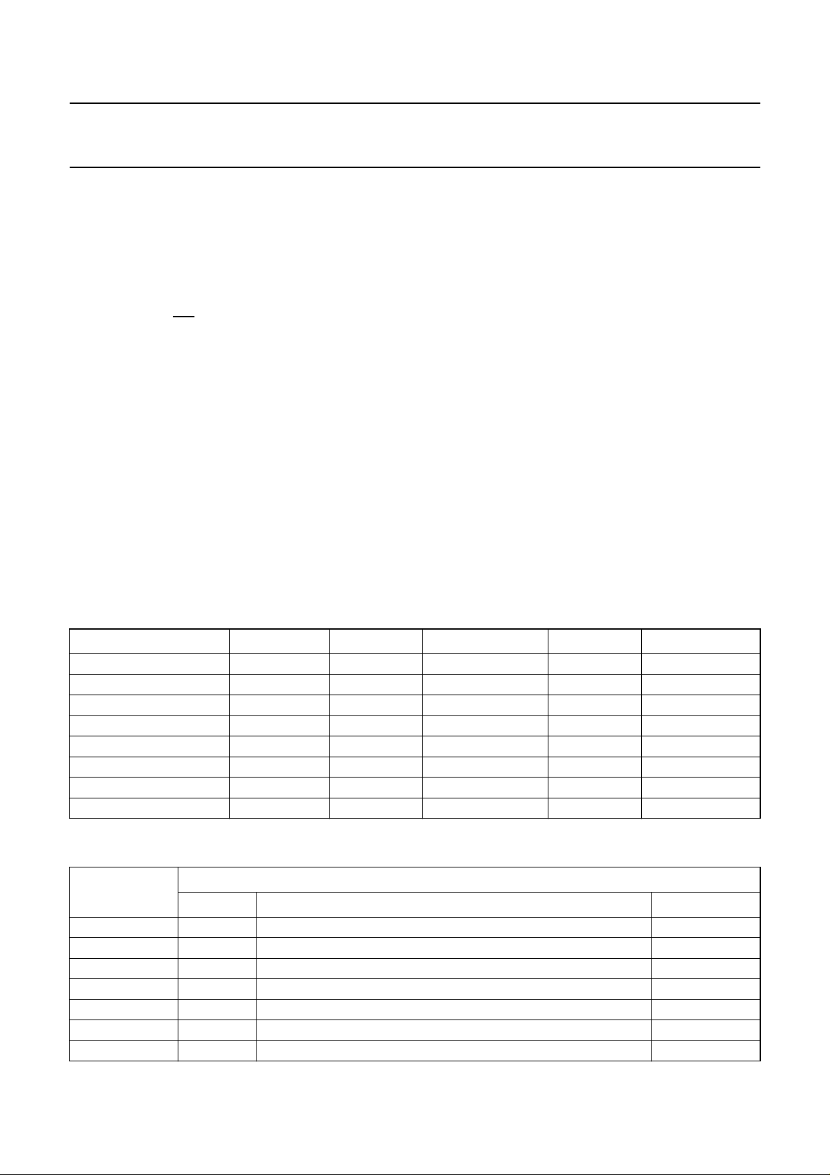
4 BLOCK DIAGRAMS
LOUT
DRIVER
OUTPUT
DD
V
metal option
andbook, full pagewidth
XTAL1
XTAL2
OSCILLATOR
ILOUT
HMINT
HARDWARE
MODULATOR
DAO to DA7
DXALE, DXWR, DXRD
T0/INT
PCA84C922; PCA84C923
MBE347
T0/INT
INTO
P10P12P14P16
P11P13P15P17
RAM
256 bytes
84CXX CORE
ROM
8 kbytes
DP65toDP60
OE
address (MSB)
30
TIMER
WATCHDOG
DD
V
RSTO
RESET
T1
LATCH
DPORT 6
DP67toDP60
DP67 to DP65
P23toP20
RDD5
CONTROL
CODING TABLE
LATCH
DPORT 5
EMU
DP57toDP50
PORT 0
(LSB)
address
ROM
16 kbytes
CODING TABLE
P07 to P00
Fig.1 Block diagram - PCA84C923D.
SS
V
1997 Oct 22 4
Page 5
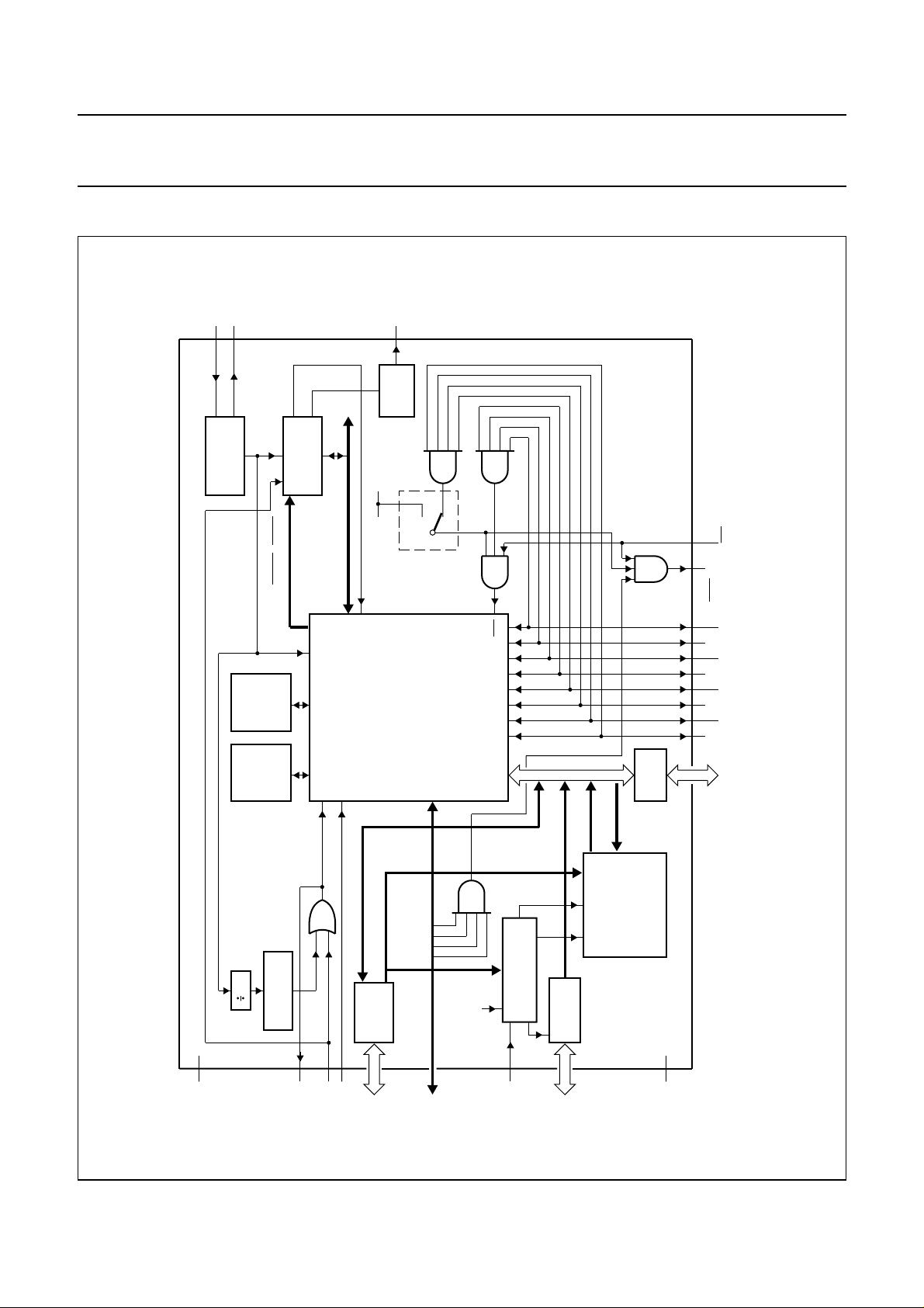
Philips Semiconductors Product specification
Microcontrollers for universal infrared
remote transmitter applications
XTAL1
XTAL2
OSCILLATOR
ILOUT
HMINT
HARDWARE
MODULATOR
DAO to DA7
LOUT
DRIVER
OUTPUT
DD
V
metal option
PCA84C922; PCA84C923
MBE413
T0/INT
DXALE, DXWR, DXRD
RAM
bytes
128/256
ROM
8 kbytes
30
TIMER
WATCHDOG
84CXX CORE
address (MSB)
LATCH
DPORT 6
DP67 to DP65
T0/INT
RDD5
DP65toDP60
CONTROL
CODING TABLE
EMU
ROM
OE
PORT 0
(LSB)
address
8/16 kbytes
CODING TABLE
P10P12P14P16
P11P13P15P17
handbook, full pagewidth
P07 to P00
Fig.2 Block diagram - PCA84C922C and PCA84C923C.
DD
V
T1
RESET
P23toP20
1997 Oct 22 5
SS
V
Page 6
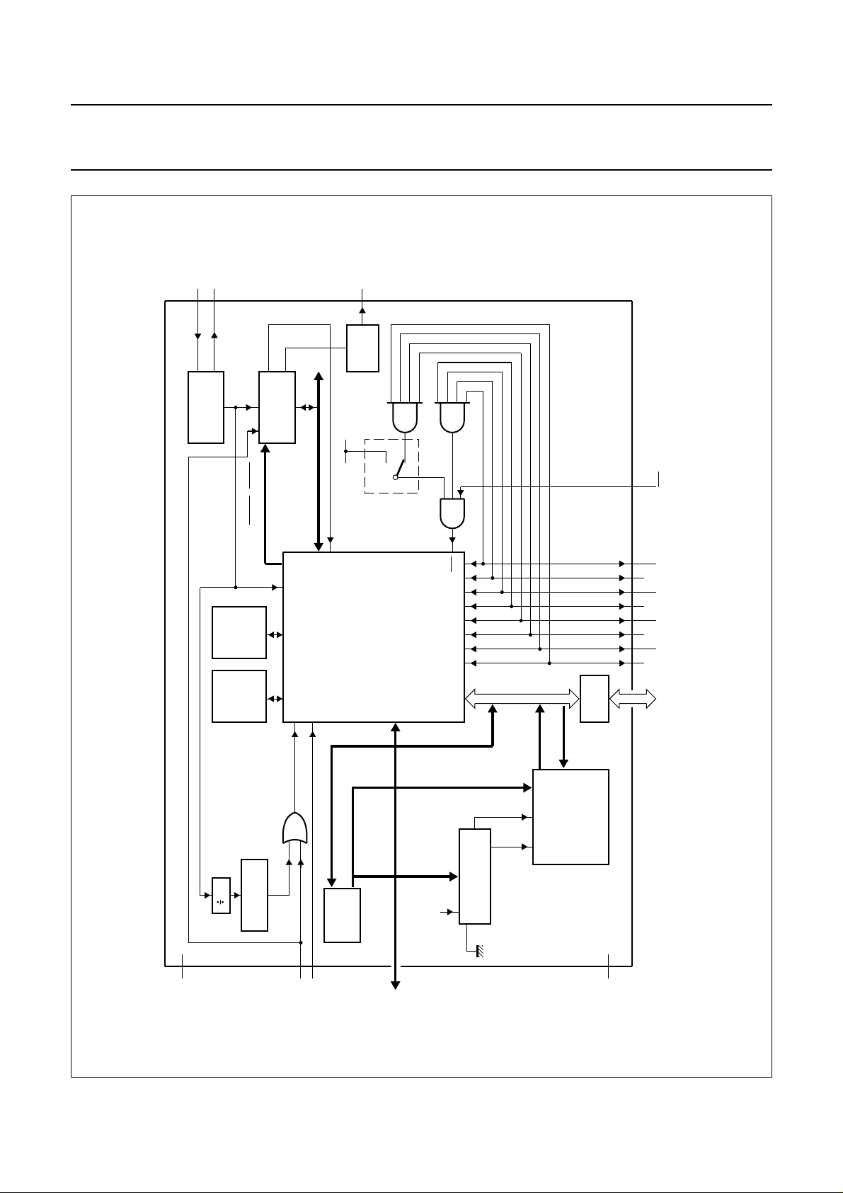
Philips Semiconductors Product specification
Microcontrollers for universal infrared
remote transmitter applications
XTAL1
XTAL2
OSCILLATOR
ILOUT
HMINT
HARDWARE
MODULATOR
DAO to DA7
LOUT
DRIVER
OUTPUT
DD
V
metal option
PCA84C922; PCA84C923
MBE414
T0/INT
DXALE, DXWR, DXRD
RAM
bytes
128/256
ROM
8 kbytes
30
TIMER
WATCHDOG
84CXX CORE
address (MSB)
LATCH
DPORT 6
T0/INT
RDD5
DP65toDP60
CONTROL
CODING TABLE
EMU
ROM
OE
PORT 0
(LSB)
address
8/16 kbytes
CODING TABLE
P10P12P14P16
P11P13P15P17
handbook, full pagewidth
P07 to P00
Fig.3 Block diagram - PCA84C922A and PCA84C923A.
DD
V
T1
RESET
1997 Oct 22 6
SS
V
Page 7
Philips Semiconductors Product specification
Microcontrollers for universal infrared
remote transmitter applications
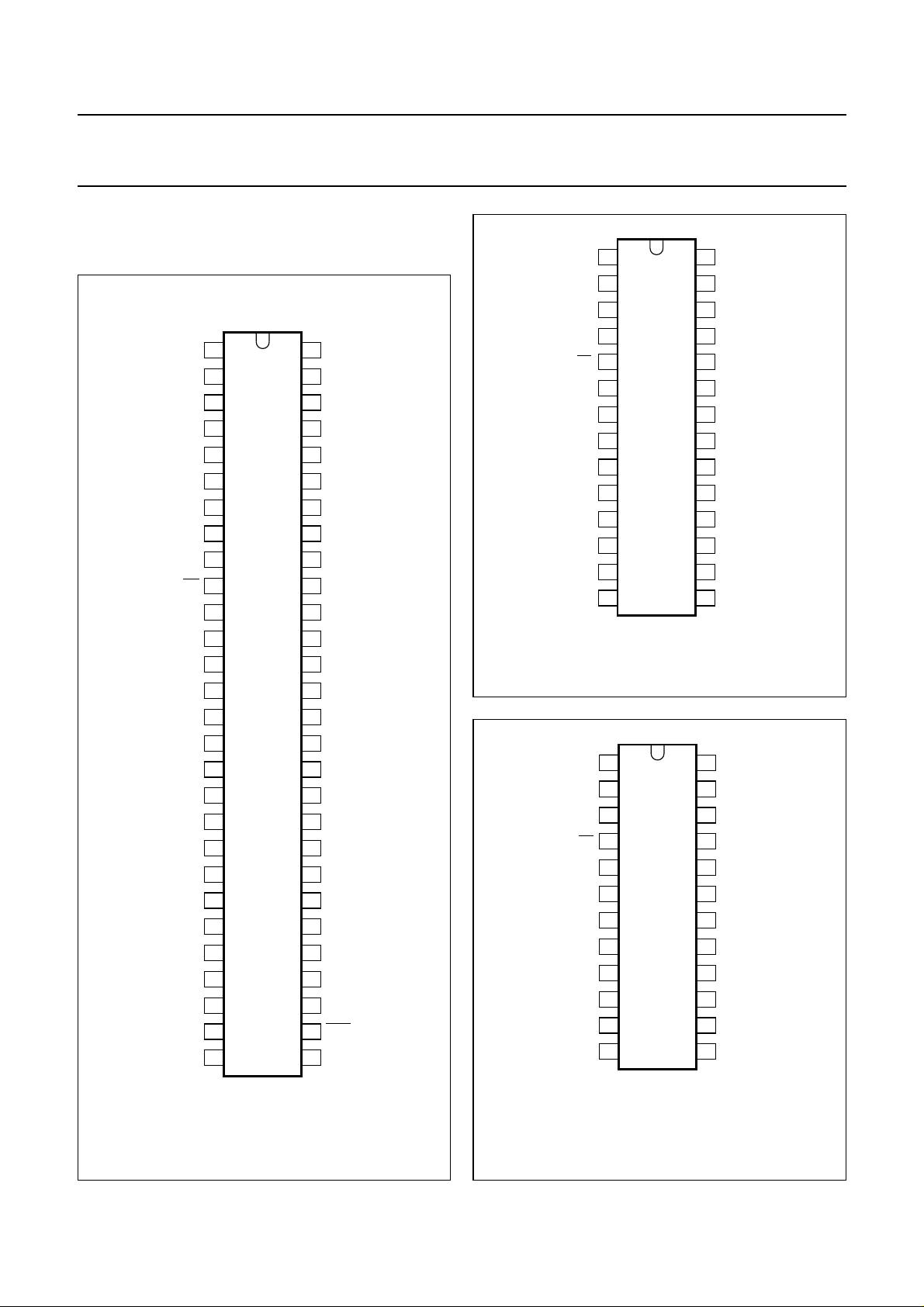
5 PINNING INFORMATION
5.1 Pinning
handbook, halfpage
RSTO
V
SS
P22
P14
DP57
P01
P00
n.c.
DP56
T0/INT
T1
DP55
RESET
DP54
DP53
V
DD
DP52
XTAL2
XTAL1
n.c.
n.c.
P04
DP51
P05
DP50
P16
P20
DP60
1
2
3
4
5
6
7
8
9
10
11
12
13
14
PCA84C923D
15
16
17
18
19
20
21
22
23
24
25
26
27
28
MBE343
P23
56
55
P15
DP67
54
EMU
53
P02
52
P03
51
50
n.c.
49
n.c.
n.c.
48
LOUT
47
V
46
SS
DP66
45
P10
44
DP65
43
42
DP64
41
P11
DP63
40
39
P12
P13
38
n.c.
37
36
n.c.
35
P07
P06
34
DP62
33
P17
32
DP61
31
INTO
30
P21
29
PCA84C922; PCA84C923
handbook, halfpage
RESET
Fig.5 Pin configuration of PCA84C922C
(SO28) and PCA84C923C (SO28).
handbook, halfpage
RESET
P22
P14
P01
P00
T0/INT
V
DD
XTAL2
XTAL1
P04
P05
P16
P20
P14
P01
P00
T0/INT
V
DD
XTAL2
XTAL1
P04
P05
P16
T1
T1
1
2
3
4
5
6
7
PCA84C922C
PCA84C923C
8
9
10
11
12
13
14
1
2
3
4
5
6
PCA84C922A
PCA84C923A
7
8
9
10
11
12
28
27
26
25
24
23
22
21
20
19
18
17
16
15
MBE342
24
23
22
21
20
19
18
17
16
15
14
13
MBE341
P23
P15
P02
P03
LOUT
V
SS
P10
P11
P12
P13
P07
P06
P17
P21
P15
P02
P03
LOUT
V
SS
P10
P11
P12
P13
P07
P06
P17
Fig.4 Pin configuration of PCA84C923D (VSO56).
1997 Oct 22 7
Fig.6 Pin configuration of PCA84C922A
(SO24/SDIP24) and PCA84C923A
(SO24/SDIP24).
Page 8

Philips Semiconductors Product specification
Microcontrollers for universal infrared
PCA84C922; PCA84C923
remote transmitter applications
5.2 Pin description
Table 2 PCA84C923D (VS056)
SYMBOL PIN DESCRIPTION
P00 to P07 7, 6, 52, 51, 22,
24, 34 and 35
P10 44 Port line 10 or emulation
P11 41 Port line 11 or emulation
P12 39 Port line 12 or emulation DXALE signal input.
P13 38 Port line 13 or emulation
P14 to P17 4, 55, 26 and 32 Standard I/O port lines, generally used for keypad sensing, the wake-up function
P20 to P23 27, 29, 3 and 56 Standard I/O port lines with 10 mA sink capability.
DP50 to DP57 25, 23, 17, 15, 14,
12, 9 and 5
DP60 to DP67 28, 31, 33, 40, 42,
43, 45 and 54
RSTO 1 Used for emulation purposes only. This output is the result of the OR operation
T0/
INT 10 Test pin T0 or external interrupt input.
T1 11 Test pin T1 or timer/counter input (T1).
RESET 13 Active HIGH reset pin; normally connected to V
XTAL2 18 Crystal or ceramic resonator or LC oscillator connections.
XTAL1 19
INTO 30 Used for emulation purposes only and is connected to the T0/INT pin of the
LOUT 47 Pulse train output pin, capable of sinking 30 mA.
EMU 53 Emulation mode control pin; for normal operation this pin is connected to V
V
DD
V
SS
16 Power supply.
2 and 46 Ground.
Standard I/O Port lines, generally used for keypad scanning or for LSB address
lines of coding table.
DXWR signal input.
DXRD signal input.
EXDI signal input.
can be removed by mask option.
Standard I/O port lines, generally used for the data bus of Coding Table.
Standard I/O Port lines, generally used for keypad scanning or for MSB address
lines of Coding Table.
carried out internally on the RESET input and the Watchdog Timer reset and is
connected to the RESET pin of the 84C00.
as Power-on-reset serves the
SS
same function.
84C00.
SS
.
1997 Oct 22 8
Page 9
Philips Semiconductors Product specification
Microcontrollers for universal infrared
PCA84C922; PCA84C923
remote transmitter applications
Table 3 PCA84C922C (SO28) and PCA84C923C (SO28)
SYMBOL PIN DESCRIPTION
P00 to P07 4, 3, 26, 25,
11, 12, 17, 18
P10 to P17 22, 21, 20, 19,
2, 27, 13, 16
P20 to P23 14, 15, 1, 28 Standard I/O port lines with 10 mA sink capability.
T0/
INT 5 Test pin T0 or external interrupt input.
T1 6 Test pin T1 or timer/counter input (T1).
RESET 7 Active HIGH reset pin; normally connected to V
XTAL2 9 Crystal or ceramic resonator or LC oscillator connections.
XTAL1 10
LOUT 24 Pulse train output pin, capable of sinking 30 mA.
V
DD
V
SS
8 Power supply.
23 Ground.
Standard I/O port lines, generally used for keypad scanning or for LSB address byte of
code data.
Standard I/O port lines, generally used for keypad sensing, the wake-up function of
P14 to P17 can be removed by mask option.
as Power-on-reset serves the same
SS
function.
Table 4 PCA84C922A (SO24/SDIP24) and PCA84C923A (SO24/SDIP24)
SYMBOL PIN DESCRIPTION
P00 to P07 3, 2, 23, 22,
10, 11, 14, 15
P10 to P17 19,18, 17, 16,
1, 24,12,13
T0/
INT 4 Test pin T0 or external interrupt input.
Standard I/O port lines, generally used for keypad scanning or for LSB address byte of
code data.
Standard I/O port lines, generally used for keypad sensing, the wake-up function of
P14 to P17 can be removed by mask option.
T1 5 Test pin T1 or timer/counter input (T1).
RESET 6 Active HIGH reset pin; normally connected to V
as Power-on-reset serves the same
SS
function.
XTAL2 8 Crystal or ceramic resonator or LC oscillator connections.
XTAL1 9
LOUT 21 Pulse train output pin, capable of sinking 30 mA.
V
DD
V
SS
7 Power supply.
20 Ground.
1997 Oct 22 9
Page 10

Philips Semiconductors Product specification
Microcontrollers for universal infrared
remote transmitter applications
6 GENERAL OPERATION DESCRIPTION
The main application for the PCA84C92X is as a universal
infrared remote control commander and in this role the
PCA84C92X offers the complete solution in one chip.
The PCA84C92X can be programmed to generate code
data that conforms to any protocol (Philips, NEC, RCA,
Thomson and Siemens etc.) and is suitable for use in the
remote control of TVs, VCRs, audio equipment,
air-conditioning systems and in many other applications.
The ability of the PCA84C923D to access external
memory and therefore support more protocols, makes it an
extremely versatile device.
6.1 System selection
Different systems (TV or VCR etc.) can be controlled using
one universal infrared remote control commander;
switches can be used to select a specific system.
However, the PCA84C92X provides pin T1 for system
selection purposes and software is used to detect the
specific system. Port lines P14 to P17 can also be used for
system selection if their wake-up functions have not been
selected as a mask option.
PCA84C922; PCA84C923
After a Power-on-reset, the scan lines are set LOW and
the sense lines HIGH. If the system has entered the Stop
mode (by software) then when any key is depressed an
external interrupt will be generated and the system will be
woken-up.
If the external interrupt was enabled (by using the ‘EN I’
instruction) before the Stop mode was entered, then when
the CPU is woken-up, the instruction that follows the STOP
instruction will be executed before diverting to the interrupt
routine at vector address 03H. However, if the interrupt
was not enabled before the Stop mode was entered, then
when the CPU is woken-up the instruction that follows the
STOP instruction will be executed.
6.3 Accessing command code
When any key is depressed its function and operation
protocol are determined, then the command code is read.
If the command code is stored in system ROM it can be
accessed using the ‘MOVP A,@A’ instruction. If the
command code resides in Coding Table ROM it can be
accessed by writing the address to DP60 to DP67 (High
byte) and P00 to P07 (Low byte) and then reading the data
from DP50 to DP57.
When no key is pressed the scan lines (Port 0) can be
programmed HIGH and the sense lines (Port 1)
programmed LOW. If a diode is connected between a
sense line and scan line then the scan line will be pulled
LOW and this can be detected by a read operation to
Port 0.
6.2 Key scanning
Port lines P10 to P17 and T0/
be used as key sense lines. However, if the wake-up
option is not selected for ports P14 to P17 then these can
be used as general I/O lines.
Port lines P00 to P07, P20 to P23 and DP60 to DP67 can
be used as key scan lines or general I/O ports. Derivative
Port 6 also provides the High byte address for the Coding
Table, even when used as scan lines.
INT have been designed to
In Normal mode, if the Coding Table address is within the
0000 to 1FFFH range for PCA84C922 devices, or within
the 0000 to 3FFFH range for PCA84C923 devices, then
the internal Coding Table will be accessed when
Derivative Port 5 (address 05H) is read.
In the Normal mode only the PCA84C923D has the ability
to access external memory. If the Coding Table address is
greater than 3FFFH then the external memory will be
accessed when Derivative Port 5 (terminal) is read.
When the PCA84C923D is used in the Emulation mode,
when Derivative Port 5 is read, data will always be read
from DP50 to DP57 terminals. Therefore, the internal
Coding Table ROM can be emulated when the
PCA84C923D and the bond-out chip PCF84C00 are used.
1997 Oct 22 10
Page 11
Philips Semiconductors Product specification
Microcontrollers for universal infrared
remote transmitter applications
handbook, full pagewidth
P00
P01
P02
P03
P04
P05
T1
V
DD
XTAL1
XTAL2
PCA84C922; PCA84C923
V
DD
system selection
100 Ω
R1
P06
PCA84C922A
P07
PCA84C923A
T0/INT
P10
P11
P12
P13
P14
P15
P16
P17
LOUT
RESET
V
3.0 V
30 mA
SS
MBE416
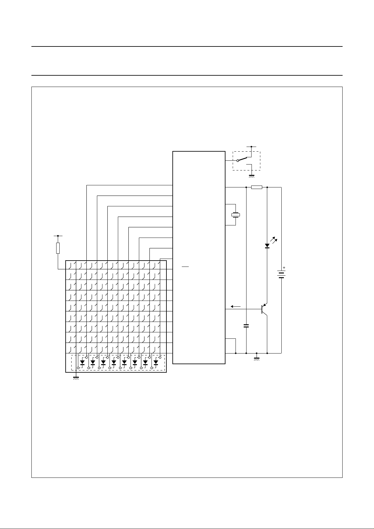
Fig.7 Typical Remote Control Transmitter application using the PCA84C922A or PCA84C923A.
1997 Oct 22 11
Page 12

Philips Semiconductors Product specification
Microcontrollers for universal infrared
remote transmitter applications
V
handbook, full pagewidth
R1
DD
R2
R3
P20
P21
P22
P23
P00
P01
P02
P03
P04
P05
P06
P07
T0/INT
P10
PCA84C922; PCA84C923
V
DD
XTAL1
XTAL2
PCA84C922C
PCA84C923C
T1
V
DD
system selection
100 Ω
3.0 V
Fig.8 Typical Remote Control Transmitter application using the PCA84C922C or PCA84C923C.
1997 Oct 22 12
P11
P12
P13
P14
P15
P16
P17
LOUT
RESET
V
30 mA
SS
MBE417
Page 13

Philips Semiconductors Product specification
Microcontrollers for universal infrared
remote transmitter applications
handbook, full pagewidth
V
DD
OE
ROM or EPROM
R2
R3
A0 to A7 A8 to A15
P20
P21
DP50 to DP57
PCA84C922; PCA84C923
V
DD
T1
V
DD
XTAL1
system selection
100 Ω
R1
DP60 to DP67
P00 to P07
PCA84C923D
T0/INT
P10
P11
P12
P13
P14
P15
P16
P17
XTAL2
LOUT
EMU
RESET
V
3.0 V
30 mA
SS
MBE418
Fig.9 Typical Remote Control Transmitter application using the PCA84C923D.
1997 Oct 22 13
Page 14

Philips Semiconductors Product specification
Microcontrollers for universal infrared
remote transmitter applications
7 HARDWARE MODULATOR
The Hardware Modulator used in the PCA84C92X is the
same as the Hardware modulator used in the PCA84CX22
range of microcontrollers.
The function of the Hardware Modulator is to generate a
coded pulse train which is subsequently converted into an
infrared signal by an IR-LED. It is this coded IR signal that
controls the remote equipment. The number of pulses in
the pulse train, the time between pulse train bursts and the
duty cycle of a pulse are all programmable. A typical pulse
train is shown in Fig.10.
The block diagram of the Hardware Modulator is shown in
Fig.14 and comprises:
• An 8-bit ON-time Register
• An 8-bit OFF-time Register
• An 8-bit Control Register
• A Pulse Timer
• A 10-bit Pulse Counter
• Control logic.
These are described in detail in Sections 7.1 to 7.5.
PCA84C922; PCA84C923
7.2 OFF-time Register
This 8-bit register resides at address 01H and is loaded by
software. The decimal value of its contents plus 2,
determines the number of oscillator cycles that the LOUT
pin is inactive.
The inactive period of LOUT can be calculated as follows:
t
OFF
7.3 Pulse Timer
The contents of the ON-time and OFF-time Registers are
loaded alternately into the Pulse Timer. When loaded the
Pulse Timer contents are decremented by ‘1’ every
oscillator cycle and upon reaching zero the Pulse Timer
will be reloaded with the contents of the other register.
7.4 Pulse Counter
The 10-bit Pulse Counter actually consists of two registers:
the 2-bit Pulse Counter High Register that resides at
address 04H, and the 8-bit Pulse Counter Low Register
that resides at address 02H.
decimal value held in OFF-time Register 2+()
=
--------------------------------------------------------------------------------------------------------------------------f
osc
7.1 ON-time Register
The duty cycle of the pulse is determined by the contents
of the ON-time and OFF-time Registers. The ON-time
Register controls the active or ON period of the pulse; the
OFF-time Register controls the inactive or OFF period of
the cycle.
The 8-bit ON-time Register resides at address 00H and is
loaded by software. The decimal value of its contents
plus 2, determines the number of oscillator cycles that the
LOUT pin is active. The active period of LOUT can be
calculated as follows:
decimal value held in ON-time Register 2+()
=
t
------------------------------------------------------------------------------------------------------------------------
ON
f
osc
The Pulse Counter is loaded by software; its contents
determine the number of pulses in a specific pulse train.
Loading with zero is not allowed.
7.5 Hardware Modulator Control Register (HMCTL)
The characteristics of the pulse train are initially
determined by the contents of the ON-time Register, the
OFF-time Register and the Pulse Counter; however, the
HMCTL Register allows these characteristics to be
modified. The Watchdog Timer and derivative interrupt
flag are reset via this register.
1997 Oct 22 14
Page 15

Philips Semiconductors Product specification
Microcontrollers for universal infrared
PCA84C922; PCA84C923
remote transmitter applications
Table 5 Hardware Control Register (address 03H)
76543210
−−−WRES Rint PWM LgP HF
Table 6 Description of the HMCTL bits
BIT SYMBOL DESCRIPTION
7 to 5 − These three bits are reserved.
4 WRES Reset Watchdog Timer . This is not a flip-flop in the register and can only be written to. If a logic 1
is written to this bit the Watchdog Timer is reset.
3 Rint Reset interrupt. When Rint = 1; the interrupt flag that was set by the derivative logic is cleared.
The Hardware Modulator can only be restarted after the interrupt flag is cleared; this avoids a
second interrupt being generated before the first one has been serviced.
2 PWM Pulse Width Modulation. When PWM = 1 and LgP = 0; the Pulse Counter Register is ignored
and a continuous pulse train is generated, this is shown in Fig.13.
1 LgP Long Pulse. When LgP = 1; the contents of the OFF-time Register are ignored. A single pulse is
generated; its pulse width being determined as shown below.
1
Pulse width Contents of ON-time Register 2+()number of pulses()
1
⁄4f
If HF = 1; this pulse is modulated with a frequency
, this is shown in Fig.12.
osc
0 HF High Frequency. When HF = 1; the ON-time part of the generated pulse is modulated with a
1
⁄4f
frequency
, this is shown as CASE 2 in Figs 11 and 12.
osc
××=
-------f
osc
handbook, full pagewidth
ILOUT
start
ON-time
OFF-time
end
interrupt
pulse #1 pulse #2 pulse #3
OFF-time = 4 (off-time register = 2)ON-time = 2 (on-time register = 0) number of pulses = 3
Fig.10 Example of ILOUT pulse train.
elapse time by software
MBE345
1997 Oct 22 15
Page 16

Philips Semiconductors Product specification
Microcontrollers for universal infrared
remote transmitter applications
f
osc
handbook, full pagewidth
f
osc
4
f
osc
4
ILOUT
ILOUT
start start
CASE 1
On-time Register = 6
on-time pulse width = 6 2 = 8
CASE 2
Off-time Register = 10
off-time pulse width = 10 2 = 12
Fig.11 CASE 1 shows a typical pulse train; CASE 2 shows the same pulse
train after being modulated with a frequency of1⁄4f
number of pulses = 2
PCA84C922; PCA84C923
software time
interrupt to CPU
MBE412
(HF = 1).
osc
f
handbook, full pagewidth
osc
f
osc
4
f
osc
4
ILOUT
CASE 1
ILOUT
CASE 2
f
osc
handbook, full pagewidth
f
osc
4
f
osc
4
ILOUT
start
On-time Register = 10
on-time pulse width = 10 2 = 12
number of pulses = 3
Fig.12 CASE 1 shows a typical long pulse; CASE 2 shows the same long
pulse after being modulated with a frequency of1⁄4f
start
On-time Register = 10
on-time pulse width = 10 2 = 12
Off-time Register = 10
off-time pulse width = 10 2 = 12
(HF = 1).
osc
software time
interrupt to CPU
MBE411
MBE410
Fig.13 Continuous pulse train (PWM = 1).
1997 Oct 22 16
Page 17

Philips Semiconductors Product specification
Microcontrollers for universal infrared
remote transmitter applications
7.6 Operation of the Hardware Modulator
The ON-time, OFF-time, Pulse Counter High and Pulse
Counter Low registers are loaded by software.
As soon as the Pulse Counter Low Register is loaded the
Hardware Modulator is started and LOUT becomes active
(LOW). Simultaneously, the contents of the ON-time
Register are loaded into the Pulse Timer which is then
decremented by ‘1’ every oscillator clock cycle. When the
value held in the Pulse Timer becomes zero the contents
of the Pulse Counter are decremented by ‘1’ and LOUT
becomes inactive (HIGH).
The contents of the OFF-time Register are now loaded into
the Pulse Timer which is decremented by ‘1’ every
oscillator clock cycle. When the value held in the Pulse
Timer becomes zero, LOUT becomes active (LOW). One
pulse cycle has now been generated.
PCA84C922; PCA84C923
The process of alternately loading the contents of the
ON-time Register and OFF-time Register into the Pulse
Timer continues until the contents of the Pulse Counter
become zero. When this occurs
interrupt to the CPU is generated and the interrupt flag is
raised stopping the operation of the Hardware Modulator.
The programmed pulse train has now been generated.
The Hardware Modulator can only be restarted after the
interrupt flag has been cleared. The interrupt flag is
cleared by writing a logic 1 to the Rint bit in the Hardware
Modulator Control Register.
The time delay between two pulse trains is determined by
software.
EXDI is asserted; an
handbook, full pagewidth
internal bus (IB0 to 7)
f
osc
DXALE
DXWR
EXDI
ON-TIME
REGISTER
(8)
PULSE TIMER
(8)
OFF-TIME
REGISTER
(8)
CONTROL LOGIC
PULSE COUNTER
HIGH
Fig.14 Block diagram of the Hardware Modulator.
(2)
CONTROL
REGISTER
(5)
PULSE COUNTER
LOW
(8)
ILOUT
MBE346
1997 Oct 22 17
Page 18

Philips Semiconductors Product specification
Microcontrollers for universal infrared
remote transmitter applications
8 CODING TABLE
The code data transmitted from the LOUT output when any
key is depressed, is stored in a memory area known as the
Coding Table. The PCA84C92X range of microcontrollers
have on-chip ROM specifically for this use (system ROM
may also be used). The Coding Table is addressed via
Port 0 (the Low byte address) and Derivative Port 6 latch
(the High byte address).
The PCA84C922 range of devices have 8 kbytes of ROM
for use as a Coding Table and when accessing this internal
memory, address lines DP65 to DP67 must be LOW.
The PCA84C923 range of devices have 16 kbytes of ROM
for use as a Coding Table and when accessing this internal
memory, address lines DP66 and DP67 must be LOW.
The Coding Table memory size for the PCA84C923D
however, can be extended up to 64 kbytes by adding
external memory (ROM or EPROM). The external memory
data bus is connected to Derivative Port 5. Accessing the
internal or external Coding Tables of the PCA84C923D is
described below.
• In the Normal mode (EMU pin LOW)
– When Derivative Port 5 terminal is read, if the
address lines DP66 and DP67 are LOW, the address
will be within the internal memory boundary, and the
internal Coding Table will be accessed.
– When Derivative Port 5 terminal is read, if either of
the address lines DP66 or DP67 is HIGH, the address
will be outside the internal memory boundary and the
external memory will be accessed. The data at
Derivative Port 5 terminal will then be read.
PCA84C922; PCA84C923
• In the Emulation mode (EMU pin HIGH)
– When Derivative Port 5 terminal is read, external
memory will always be accessed. In this situation,
Derivative Port 5 latch cannot be read.
8.1 Accessing the Coding Table
The procedure for accessing the Coding Table follows:
1. Set all sense lines to a logic 1.
2. Write the High byte address to Derivative Register 08
(Derivative Port 6 latch).
3. Write the Low byte address to Port 0 (Low byte
address latch of internal Coding Table).
4. Read Derivative Register 05 (Derivative Port 5
terminal); code data has now been retrieved.
5. Repeat steps 4 and 5 to read more code data.
Table 7 shows a subroutine that reads the Coding Table
and then loads code data into system RAM.
Entry:
R0 contains the starting address in system RAM into
which data will be loaded.
R1 contains the number of bytes in the Coding Table
which are to be read.
R3 holds the Coding Table starting address (Low byte).
R4 holds the Coding Table starting address (High byte).
Exit:
((R0)), ((R0) + 1) →((R0) + (R1) − 1) contain the code
data
Table 7 Subroutine to access the Coding Table
ADDRESS INSTRUCTION DESCRIPTION
CODE ORL P1,#FF Set all sense lines to logic 1.
MOV A,R4 Load Accumulator with the High byte of the starting address.
MOV D8,A Write the High byte of the starting address to Derivative Port 6 latch.
CODE1 MOV A,R3 Load Accumulator with the Low byte of the starting address.
OUTL P0,A Write the Low byte of the starting address to Port 0.
MOV A,D5 Read code data from Derivative Port 5 terminal into the Accumulator.
MOV @R0,A Store code data in system RAM.
DJNZ R1,CODE2 If more code data is to be read jump to CODE 2, if not go to next instruction.
RET Return from subroutine to main program.
CODE2 INC R0 Increment RAM address pointer.
INC R3 Increment Low byte address of Coding Table.
JMP CODE1 Jump to CODE 1.
1997 Oct 22 18
Page 19

Philips Semiconductors Product specification
Microcontrollers for universal infrared
remote transmitter applications
9 WATCHDOG TIMER (WDT)
The PCA84C92X contains a Watchdog Timer that
functions in the same manner as the Watchdog Timer
used in the PCA84CX22 range of microcontrollers.
The purpose of the Watchdog Timer is to reset the
microcontroller if it enters an erroneous processor state;
within a reasonable period of time. Erroneous processor
states can be caused by noise or RFI.
The Watchdog Timer consists of a 17-bit counter which is
clocked at a frequency of1⁄30f
the contents of the counter are cleared. The counter
contents are then incremented by ‘1’ every 30 cycles of the
oscillator clock. If the maximum count is exceeded, the
counter overflows and the microcontroller is reset. In order
to prevent a counter overflow and its resulting reset
operation, the user program must clear the contents of the
Watchdog Timer before its maximum count is reached.
. During a Power-on-reset
osc
PCA84C922; PCA84C923
During normal processing, the contents of the Watchdog
Timer are cleared by writing a logic 1 to the WRES bit in
Hardware Modulator Control Register (address 03H).
The maximum time period (tp) which the counter may run
and not cause a reset operation, is calculated as shown
below.
30 2
××=
16
1
t
--------
p
f
osc
In the Idle mode the oscillator is still running and the
Watchdog Timer remains active. In the Stop mode
however, the oscillator is stopped and the operation of the
Watchdog Timer is halted but its contents are retained.
Therefore, it may be advisable for the user to clear the
contents of the Watchdog Timer before the Stop mode is
entered, in order to avoid an unexpected reset operation
after the device is woken-up.
handbook, full pagewidth
f
osc
Power-on-reset
30
HMCTL register (address O3H)
R
WRES
PWM HF
int
Fig.15 Block diagram of the Watchdog Timer.
L P
g
CLK
RESET
17-BIT COUNTER
Q16
on-chip RESET
MBE415
1997 Oct 22 19
Page 20

Philips Semiconductors Product specification
Microcontrollers for universal infrared
remote transmitter applications
10 PORT OPTIONS
Ports can be configured using one of three mask options.
The three I/O mask options are specified below.
Option 1 Standard I/O with switched pull-up current
source; this is shown in Fig.16.
Option 2 I/O with open-drain output; this is shown in
Fig.17.
Option 3 Push-pull output; this is shown in Fig.18.
The state of the ports and the LOUT pin after a
Power-on-reset can also be selected using mask options.
All mask options are given in Table 8.
Table 8 Mask options
PORT LINES/PIN S R OPTION
P00 to P07 1 or 3; notes 1 and 2
P10 to P13 X 1; note 3
P14 to P17 1; note 3
P20 to P23
DP50 to DP57 X 1
DP60 to DP67 1 or 3; notes 1, 2 and 4
LOUT X 2 or 3
PCA84C922; PCA84C923
Notes to Table 8
1. If diodes are used for system selection the scan lines
(Port 0 and Derivative Port 6) cannot take Option 3.
2. Scan lines should have the option ‘1R’.
3. Sense lines should have the option ‘1S’.
4. Only the PCA84C923D has external Derivative Port 6
terminals and therefore this option is only valid for this
device. The other members of the range have the state
of their internal Derivative Port 6 latch fixed at ‘1S’.
handbook, full pagewidth
write pulse
OUTL/ORL/ANL/MOV
data bus
DDMQ SQ
ORL/ANL/MOV
Master Slave
SQ
IN/MOV
Fig.16 Standard I/O with switched pull-up current source (Option 1).
1997 Oct 22 20
TR2
TR1
V
DD
100 µA typical (V = 0.7 V )
TR3
I/O port
line
V
SS
MED186 - 1
DD
O
Page 21

Philips Semiconductors Product specification
Microcontrollers for universal infrared
remote transmitter applications
handbook, full pagewidth
write pulse
OUTL/ORL/ANL
data bus
DDMQ SQ
Master Slave
ORL/ANL
PCA84C922; PCA84C923
V
DD
TR1
V
SS
IN
I/O port
line
MED187 - 1
handbook, full pagewidth
write pulse
OUTL/ORL/ANL
data bus
Fig.17 I/O with open-drain output (Option 2).
TR2
DDMQ SQ
Master Slave
TR1
V
ORL/ANL
IN
SS
V
DD
I/O port
line
MED188
Fig.18 Push-pull output (Option 3).
1997 Oct 22 21
Page 22

Philips Semiconductors Product specification
Microcontrollers for universal infrared
remote transmitter applications
11 INTERRUPTS
The PCA84C92X has three interrupt sources:
1. External keypad wake-up and T0/INT pin; vector
address 03H.
2. Hardware Modulator; vector address 05H.
3. Internal Timer/counter (T1); vector address 07H.
11.1 External keypad wake-up and T0/
interrupt
This interrupt will wake-up the CPU from the Stop mode
when a HIGH-to-LOW transition occurs on any Port 1 pin
or the T0/
will continue after a 1866 clock cycle delay.
If this interrupt was enabled (by using the ‘EN I’ instruction)
before the Stop mode was entered, then when the CPU is
woken-up, the instruction that follows the STOP instruction
will be executed before diverting to the interrupt routine at
vector address 03H. However, if the interrupt was not
enabled before the Stop mode was entered, then when the
CPU is woken-up the instruction that follows the STOP
instruction will be executed.
INT pin (see Fig.1); normal program execution
INT pin
PCA84C922; PCA84C923
12 DERIVATIVE REGISTERS
The Derivative Registers residing at addresses 00 to 04H
are dedicated to the Hardware Modulator; these registers
are also common to the PCA84CX22 range of
microcontrollers. The Derivative Registers residing at
addresses 05 to 08H are used for accessing the Coding
Table. The Derivative Registers memory map is shown in
Table 9.
When the Coding Table is accessed data will be read from
Derivative Port 5 terminal (address 05H) regardless of
whether the internal or external Coding table was
addressed. Details of accessing the internal or external
Coding Tables are given in Section 8. As Derivative Port 6
latch is also connected to the High byte address of the
internal Coding Table, writing data to Derivative Port 6
latch (address 08H) also addresses the Coding Table.
11.2 Hardware Modulator interrupt
When a complete pulse train has been transmitted by the
Hardware Modulator, it generates an interrupt to the CPU
by asserting
Modulator is halted. This derivative interrupt is shared with
the SIO interrupt of the PCF84CXXXA family; both use
vector address 05H. The Hardware Modulator interrupt is
enabled using the instruction ‘EN SI’ and is disabled using
the ‘DIS SI’ instruction.
11.3 Internal Timer/counter (T1) interrupt
The Timer/counter and its interrupt are common to other
members of the PCF84CXXXA family; all operate in a
similar manner. The Timer/counter interrupt is enabled
using the instruction ‘EN TCNT1’ and is disabled using the
‘DIS TCNT1’ instruction.
EXDI and the operation of the Hardware
1997 Oct 22 22
Page 23

1997 Oct 22 23
Table 9 Derivative Registers memory map (see note 1)
ADDR
(HEX)
00 ON-TIME ON7
01 OFF-TIME OFF7
02 Pulse Counter Low
03 Hardware Modulator
04 Pulse Counter High
05 Derivative Port 5
06 Derivative Port 6
07 Derivative Port 5
08 Derivative Port 6
REGISTER 7 6 5 4 3 2 1 0 R/W
(X)
(X)
PUL7
(PULOW)
Control (HMCTL)
(PUHIGH)
(terminal)
(terminal)
(latch)
(latch)
(X)
−−−WRES
−−−−−−PUL9
DP57/MD7
(X)
DP67
(X)
DP57
(1)
DP67/MA15
(Mo)
ON6
(X)
OFF6
(X)
PUL6
(X)
DP56/MD6
(X)
DP66
(X)
DP56
(1)
DP66/MA14
(Mo)
ON5
(X)
OFF5
(X)
PUL5
(X)
DP55/MD5
(X)
DP65
(X)
DP55
(1)
DP65/MA13
(Mo)
ON4
(X)
OFF4
(X)
PUL4
(X)
(2)
(X)
DP54/MD4
(X)
DP64
(X)
DP54
(1)
DP64/MA12
(Mo)
ON3
(X)
OFF3
(X)
PUL3
(X)
(2)
Rint
(X)
DP53/MD3
(X)
DP63
(X)
DP53
(1)
DP63/MA11
(Mo)
ON2
(X)
OFF2
(X)
PUL2
(X)
PWM
(X)
DP52/MD2
(X)
DP62
(X)
DP52
(1)
DP62/MA10
(Mo)
ON1
(X)
OFF1
(X)
PUL1
(X)
LgP
(X)
(X)
DP51/MD1
(X)
DP61
(X)
DP51
(1)
DP61/MA9
(Mo)
ON0
(X)
OFF0
(X)
PUL0
(X)
HF
(X)
PUL8
(X)
DP50/MD0
(X)
DP60
(X)
DP50
(1)
DP60/MA8
(Mo)
R/W
R/W
R/W
R/W
R/W
R
R
R/W
R/W
Philips Semiconductors Product specification
Microcontrollers for universal infrared
remote transmitter applications
Notes
1. Values within parenthesis show the bit state after a reset operation. ‘X’ denotes an undefined state and ‘Mo’ denotes the state is selected by mask
option.
2. These bits are Write only.
PCA84C922; PCA84C923
Page 24

Philips Semiconductors Product specification
Microcontrollers for universal infrared
remote transmitter applications
13 EMULATION
The PCA84C923D can be used as the emulation chip for
both the PCA84C92X and PCA84CX22 ranges of
microcontrollers. The emulation system is shown in Fig.19.
A 64 kbyte EPROM (27C256) is used as the Coding Table
and stores all data code. The EPROM should be removed
when members of the PCA84CX22 range are being
emulated.
The PCA84C923D has two additional outputs: INTO and
RSTO which are used for emulation purposes only. The
INTO output is the result of the AND operation carried out
internally on the T0/INT and Port 1 inputs; this is shown in
Fig.1. The RSTO output is the result of the OR operation
carried out internally on the RESET input and the
Watchdog Timer reset; this is also shown in Fig.1. The
INTO and RSTO pins of the PCA84C923D are connected
to the T0/INT and RESET pins of the bond-out chip,
respectively.
The RESET and T0/INT inputs are connected to the
corresponding pins of the PCA84C923D (in other 84CXXX
emulation systems they are connected to the
corresponding pins of the PCF84C00).
PCA84C922; PCA84C923
In the emulation mode, port lines P10 to P13 of the
PCA84C923D are used as the inputs for derivative control
signals
port lines P20 to P23 (which are ANDed internally to
emulate the wake-up function of port lines P10 to P13) are
connected to port lines P10 to P13 of the bond-out chip.
If port lines P14 to P17 of the PCA84C923D have been
masked for the wake-up function, then they must not be
connected to the corresponding pins of the bond-out chip.
However, these sets of pins can be connected if the
wake-up option has not been selected.
When the PCA84C923D is used as the emulation chip all
ports should have the mask option 1S. After a
Power-on-reset the only data that can be written to
Derivative Port 5 is FFH.
When the PCF84C00 is used for emulation purposes its
ports should have the mask option 1S. However, as some
ports may be used as scan lines (for example Port 1 and
Port 6) they will have mask options of 1R or 3R. In this
case, after a Power-on-reset, these ports should have 00H
written to them.
DXWR, DXRD, DXALE and EXDIN. Therefore,
1997 Oct 22 24
Page 25

Philips Semiconductors Product specification
n
Microcontrollers for universal infrared
remote transmitter applications
(EPROM OR
EMULATION
SYSTEM ROM
EMULATION RAM)
EXDI
DXRD
DXALE
DXWR
DD
V
DD
V
A00 to A12
D00 to D07
PSEN
PCA84C922; PCA84C923
MBE344
P10
P11
P12
P13
P00 to P07
DD
V
XTAL1
XTAL2T1P20 to P23
T1
XTAL1
XTAL2
P20 to P23
PCF84C00
(BOND-OUT CHIP OF 84CXX)
P00 to P07
P14 to P17
P10
P11
P12
P13
P00 to P07
P10 to P17
V
RESET
T0/INT
CLK
SS
SS
V
OE
A0 to A7
SS
V XTAL1T1 EMU
INTO
RSTO
P23
P22
P21
EMULATION
CODING TABLE
(64 kbyte EPROM, 27C256)
PCA84C923D
P20
P14 to P17
DP50 to DP57
A8 to A15 D0 to D7
P50 to DP57
DP60 to DP67
RESET
T0/INT
LOUT
T0/INT
RESET
P60 to DP67
dbook, full pagewidth
Fig.19 Emulation circuit of PCA84C922 and PCA84C923.
LOUT
1997 Oct 22 25
Page 26

Philips Semiconductors Product specification
Microcontrollers for universal infrared
PCA84C922; PCA84C923
remote transmitter applications
14 LIMITING VALUES
In accordance with the Absolute Maximum Rating System (IEC 34).
SYMBOL PARAMETER MIN. MAX. UNIT
V
DD
V
I
I
OH
I
OL
P
tot
T
amb
T
stg
supply voltage −0.5 +7.0 V
all input voltages on any pin with respect to ground (VSS) −0.5 VDD+ 0.5 V
maximum source current for all port lines −−5.0 mA
maximum sink current for all port lines − 5.0 mA
total power dissipation − 500 mW
operating ambient temperature −20 +70 °C
storage temperature −55 +125 °C
1997 Oct 22 26
Page 27

Philips Semiconductors Product specification
Microcontrollers for universal infrared
PCA84C922; PCA84C923
remote transmitter applications
15 DC CHARACTERISTICS
V
=5V±10%; VSS=0V; T
DD
SYMBOL PARAMETER CONDITIONS MIN. TYP. MAX. UNIT
Supply
V
DD
I
DD
I
DD(ID)
I
DD(ST)
operating supply voltage 2.0 3.0 5.5 V
operating supply current VDD=3V;f
supply current Idle mode VDD=3V;f
supply current Stop mode VDD=2V; T
Inputs EMU; RESET; T0/INTN; T1; P00 to P07; P!0 to P17; P20 to P23; DP50 to DP57 and DP60 to DP67
V
IL
V
IH
I
LI
LOW level input voltage 0 − 0.3VDDV
HIGH level input voltage 0.7VDD− V
input leakage current VSS< VI< V
Outputs P00 to P07; P10 to P17; DP50 to DP57; DP60 to DP67; INTN0 and RSTO
I
OL
I
OH1
I
OH2
LOW level output sink current VDD=5V; VO= 0.4 V − 12 − mA
HIGH level pull-up output source current VDD=5V; VO= 0.7V
HIGH level push-pull output source
current
= −25 to +50 °C; all voltages with respect to VSS; unless otherwise specified.
amb
= 3 MHz − 0.4 0.9 mA
xtal
V
=5V;f
DD
V
=5V;f
DD
V
=2V; T
DD
=3V; T
V
DD
V
=3V; T
DD
V
=5V; T
DD
V
=5V; T
DD
V
=5V; VO=V
DD
= 3 MHz − 0.9 1.8 mA
xtal
= 3 MHz − 0.2 0.4 mA
xtal
= 3 MHz − 0.25 0.5 mA
xtal
=25°C; note 1 − 1.2 2.4 µA
amb
=50°C; note 1 −−10.0 µA
amb
=25°C; note 1 − 1.2 2.4 µA
amb
=50°C; note 1 −−10.0 µA
amb
=25°C; note 1 − 1.2 2.4 µA
amb
=50°C; note 1 −−10.0 µA
amb
DD
DD
SS
−−±1µA
−40 −100 −µA
−−140 −400 µA
VDD=5V; VO=VDD− 0.4 V −−7.0 − mA
DD
V
Outputs P20 to P23
I
OL
I
OH1
I
OH2
LOW level output sink current VDD=3V; VO= 0.4 V 10 −− mA
HIGH level pull-up output source current VDD=5V; VO= 0.7V
V
DD
HIGH level push-pull output source
VDD=5V; VO=VDD− 0.4 V −−7.0 − mA
current
Output LOUT
I
OL
I
OH
LOW level output sink current VDD=2V; VO=1V 30 −− mA
HIGH level output source current VDD=2V; VO= 1.6 V −1.6 −− mA
Note
1. f
= 3 MHz.
xtal
1997 Oct 22 27
=5V; VO=V
SS
DD
−40 −100 −µA
−−140 −400 µA
Page 28

Philips Semiconductors Product specification
Microcontrollers for universal infrared
PCA84C922; PCA84C923
remote transmitter applications
16 AC CHARACTERISTICS
SYMBOL PARAMETER CONDITIONS MIN. TYP. MAX. UNIT
f
xtal
Transconductance
g
mL
g
mM
g
mH
Rf feedback resistor 0.3 1 3 MΩ
crystal oscillator frequency VDD= 2.5 to 5.5 V 1 − 6 MHz
V
=2to5.5V 1 − 4.5 MHz
DD
option LOW VDD= 5 V 0.3 0.7 1.4 mS
option MEDIUM VDD= 5 V 0.9 1.6 3.2 mS
option HIGH VDD= 5 V 3 4.5 9.0 mS
1997 Oct 22 28
Page 29

Philips Semiconductors Product specification
Microcontrollers for universal infrared
remote transmitter applications
17 PACKAGE OUTLINES
VSO56: plastic very small outline package; 56 leads
D
y
Z
56
PCA84C922; PCA84C923
SOT190-1
E
c
H
E
29
A
X
v M
A
pin 1 index
281
w M
b
11.1
11.0
0.44
0.43
p
scale
eHELLpQZywv θ
0.75
0.0295
e
0 5 10 mm
DIMENSIONS (inch dimensions are derived from the original mm dimensions)
mm
A
max.
3.3
0.13
0.3
0.1
0.012
0.004
3.0
2.8
0.12
0.11
0.25
0.01
p
0.42
0.30
0.017
0.012
0.22
0.14
0.0087
0.0055
UNIT A1A2A3b
inches
Note
1. Plastic or metal protrusions of 0.3 mm maximum per side are not included.
2. Plastic interlead protrusions of 0.25 mm maximum per side are not included.
(1)E(2)
cD
21.65
21.35
0.85
0.84
15.8
15.2
0.62
0.60
2.25
0.089
Q
A
2
A
1
1.6
1.4
0.063
0.055
detail X
1.45
0.2
1.30
0.057
0.008 0.004
0.051
L
p
L
0.1 0.1
0.004
(A )
A
3
θ
(1)
0.90
0.55
0.035
0.022
o
7
o
0
OUTLINE
VERSION
SOT190-1
IEC JEDEC EIAJ
REFERENCES
1997 Oct 22 29
EUROPEAN
PROJECTION
ISSUE DATE
96-04-02
97-08-11
Page 30

Philips Semiconductors Product specification
Microcontrollers for universal infrared
remote transmitter applications
SO28: plastic small outline package; 28 leads; body width 7.5 mm
D
c
y
Z
28
15
PCA84C922; PCA84C923
SOT136-1
E
H
E
A
X
v M
A
pin 1 index
1
e
0 5 10 mm
DIMENSIONS (inch dimensions are derived from the original mm dimensions)
mm
A
max.
2.65
0.10
A
0.30
0.10
0.012
0.004
1
A2A
2.45
2.25
0.096
0.089
0.25
0.01
b
3
p
0.49
0.32
0.36
0.23
0.019
0.013
0.014
0.009
UNIT
inches
Note
1. Plastic or metal protrusions of 0.15 mm maximum per side are not included.
(1)E(1) (1)
cD
18.1
7.6
17.7
7.4
0.71
0.30
0.69
0.29
14
w M
b
p
scale
eHELLpQ
1.27
0.050
10.65
10.00
0.419
0.394
1.4
0.055
Q
A
2
0.043
0.016
A
1.1
0.4
L
p
L
0.25 0.1
0.01
(A )
1
detail X
1.1
0.25
1.0
0.043
0.01
0.039
A
3
θ
ywv θ
Z
0.9
0.4
0.035
0.004
0.016
o
8
o
0
OUTLINE
VERSION
SOT136-1
IEC JEDEC EIAJ
075E06 MS-013AE
REFERENCES
1997 Oct 22 30
EUROPEAN
PROJECTION
ISSUE DATE
95-01-24
97-05-22
Page 31

Philips Semiconductors Product specification
Microcontrollers for universal infrared
remote transmitter applications
SO24: plastic small outline package; 24 leads; body width 7.5 mm
D
c
y
Z
24
13
PCA84C922; PCA84C923
SOT137-1
E
H
E
A
X
v M
A
pin 1 index
1
e
0 5 10 mm
DIMENSIONS (inch dimensions are derived from the original mm dimensions)
mm
A
max.
2.65
0.10
A1A2A
0.30
2.45
0.10
2.25
0.012
0.096
0.004
0.089
0.25
0.01
b
3
p
0.49
0.32
0.36
0.23
0.019
0.013
0.014
0.009
UNIT
inches
Note
1. Plastic or metal protrusions of 0.15 mm maximum per side are not included.
(1)E(1) (1)
cD
15.6
15.2
0.61
0.60
12
w M
b
p
scale
eHELLpQ
7.6
1.27
7.4
0.30
0.050
0.29
10.65
10.00
0.419
0.394
A
1.4
0.055
Q
2
A
1
detail X
1.1
1.1
0.4
0.043
0.016
1.0
0.043
0.039
0.25
0.01
L
p
L
(A )
0.25 0.1
0.01
A
3
θ
ywv θ
Z
0.9
0.4
0.035
0.004
0.016
o
8
o
0
OUTLINE
VERSION
SOT137-1
IEC JEDEC EIAJ
075E05 MS-013AD
REFERENCES
1997 Oct 22 31
EUROPEAN
PROJECTION
ISSUE DATE
95-01-24
97-05-22
Page 32

Philips Semiconductors Product specification
Microcontrollers for universal infrared
remote transmitter applications
SDIP24: plastic shrink dual in-line package; 24 leads (400 mil)
D
seating plane
L
Z
24
e
b
b
1
13
PCA84C922; PCA84C923
SOT234-1
M
E
A
2
A
A
1
w M
c
(e )
M
1
H
pin 1 index
1
0 5 10 mm
scale
DIMENSIONS (mm are the original dimensions)
A
A
A
UNIT b
Note
1. Plastic or metal protrusions of 0.25 mm maximum per side are not included.
mm
OUTLINE
VERSION
SOT234-1
max.
4.7 0.51 3.8
12
min.
max.
IEC JEDEC EIAJ
1.3
0.8
b
1
0.53
0.40
REFERENCES
cEe M
0.32
0.23
(1) (1)
D
22.3
21.4
9.1
8.7
E
12
(1)
Z
L
3.2
2.8
EUROPEAN
PROJECTION
M
10.7
10.2
E
12.2
10.5
e
1
w
H
0.181.778 10.16
ISSUE DATE
92-11-17
95-02-04
max.
1.6
1997 Oct 22 32
Page 33

Philips Semiconductors Product specification
Microcontrollers for universal infrared
remote transmitter applications
18 SOLDERING
18.1 Introduction
There is no soldering method that is ideal for all IC
packages. Wave soldering is often preferred when
through-hole and surface mounted components are mixed
on one printed-circuit board. However, wave soldering is
not always suitable for surface mounted ICs, or for
printed-circuits with high population densities. In these
situations reflow soldering is often used.
This text gives a very brief insight to a complex technology.
A more in-depth account of soldering ICs can be found in
our
“IC Package Databook”
18.2 SDIP
18.2.1 SOLDERING BY DIPPING OR BY WA VE
The maximum permissible temperature of the solder is
260 °C; solder at this temperature must not be in contact
with the joint for more than 5 seconds. The total contact
time of successive solder waves must not exceed
5 seconds.
The device may be mounted up to the seating plane, but
the temperature of the plastic body must not exceed the
specified maximum storage temperature (T
printed-circuit board has been pre-heated, forced cooling
may be necessary immediately after soldering to keep the
temperature within the permissible limit.
18.2.2 R
Apply a low voltage soldering iron (less than 24 V) to the
lead(s) of the package, below the seating plane or not
more than 2 mm above it. If the temperature of the
soldering iron bit is less than 300 °C it may remain in
contact for up to 10 seconds. If the bit temperature is
between 300 and 400 °C, contact may be up to 5 seconds.
18.3 SO and VSO
18.3.1 REFLOW SOLDERING
Reflow soldering techniques are suitable for all SO and
VSO packages.
EPAIRING SOLDERED JOINTS
(order code 9398 652 90011).
). If the
stg max
PCA84C922; PCA84C923
Several techniques exist for reflowing; for example,
thermal conduction by heated belt. Dwell times vary
between 50 and 300 seconds depending on heating
method. Typical reflow temperatures range from
215 to 250 °C.
Preheating is necessary to dry the paste and evaporate
the binding agent. Preheating duration: 45 minutes at
45 °C.
18.3.2 W
Wave soldering techniques can be used for all SO and
VSO packages if the following conditions are observed:
• A double-wave (a turbulent wave with high upward
pressure followed by a smooth laminar wave) soldering
technique should be used.
• The longitudinal axis of the package footprint must be
parallel to the solder flow.
• The package footprint must incorporate solder thieves at
the downstream end.
During placement and before soldering, the package must
be fixed with a droplet of adhesive. The adhesive can be
applied by screen printing, pin transfer or syringe
dispensing. The package can be soldered after the
adhesive is cured.
Maximum permissible solder temperature is 260 °C, and
maximum duration of package immersion in solder is
10 seconds, if cooled to less than 150 °C within
6 seconds. Typical dwell time is 4 seconds at 250 °C.
A mildly-activated flux will eliminate the need for removal
of corrosive residues in most applications.
18.3.3 R
Fix the component by first soldering two diagonallyopposite end leads. Use only a low voltage soldering iron
(less than 24 V) applied to the flat part of the lead. Contact
time must be limited to 10 seconds at up to 300 °C. When
using a dedicated tool, all other leads can be soldered in
one operation within 2 to 5 seconds between
270 and 320 °C.
AVE SOLDERING
EPAIRING SOLDERED JOINTS
Reflow soldering requires solder paste (a suspension of
fine solder particles, flux and binding agent) to be applied
to the printed-circuit board by screen printing, stencilling or
pressure-syringe dispensing before package placement.
1997 Oct 22 33
Page 34

Philips Semiconductors Product specification
Microcontrollers for universal infrared
PCA84C922; PCA84C923
remote transmitter applications
19 DEFINITIONS
Data sheet status
Objective specification This data sheet contains target or goal specifications for product development.
Preliminary specification This data sheet contains preliminary data; supplementary data may be published later.
Product specification This data sheet contains final product specifications.
Limiting values
Limiting values given are in accordance with the Absolute Maximum Rating System (IEC 134). Stress above one or
more of the limiting values may cause permanent damage to the device. These are stress ratings only and operation
of the device at these or at any other conditions above those given in the Characteristics sections of the specification
is not implied. Exposure to limiting values for extended periods may affect device reliability.
Application information
Where application information is given, it is advisory and does not form part of the specification.
20 LIFE SUPPORT APPLICATIONS
These products are not designed for use in life support appliances, devices, or systems where malfunction of these
products can reasonably be expected to result in personal injury. Philips customers using or selling these products for
use in such applications do so at their own risk and agree to fully indemnify Philips for any damages resulting from such
improper use or sale.
1997 Oct 22 34
Page 35

Philips Semiconductors Product specification
Microcontrollers for universal infrared
remote transmitter applications
NOTES
PCA84C922; PCA84C923
1997 Oct 22 35
Page 36

Philips Semiconductors – a worldwide company
Argentina: see South America
Australia: 34 Waterloo Road, NORTH RYDE, NSW 2113,
Tel. +61 2 9805 4455, Fax. +61 2 9805 4466
Austria: Computerstr. 6, A-1101 WIEN, P.O. Box 213, Tel. +43 160 1010,
Fax. +43 160 101 1210
Belarus: Hotel Minsk Business Center, Bld. 3, r. 1211, Volodarski Str. 6,
220050 MINSK, Tel. +375 172 200 733, Fax. +375 172 200 773
Belgium: see The Netherlands
Brazil: see South America
Bulgaria: Philips Bulgaria Ltd., Energoproject, 15th floor,
51 James Bourchier Blvd., 1407 SOFIA,
Tel. +359 2 689 211, Fax. +359 2 689 102
Canada: PHILIPS SEMICONDUCTORS/COMPONENTS,
Tel. +1 800 234 7381
China/Hong Kong: 501 Hong Kong Industrial Technology Centre,
72 Tat Chee Avenue, Kowloon Tong, HONG KONG,
Tel. +852 2319 7888, Fax. +852 2319 7700
Colombia: see South America
Czech Republic: see Austria
Denmark: Prags Boulevard 80, PB 1919, DK-2300 COPENHAGEN S,
Tel. +45 32 88 2636, Fax. +45 31 57 0044
Finland: Sinikalliontie 3, FIN-02630 ESPOO,
Tel. +358 9 615800, Fax. +358 9 61580920
France: 4 Rue du Port-aux-Vins, BP317, 92156 SURESNES Cedex,
Tel. +33 1 40 99 6161, Fax. +33 1 40 99 6427
Germany: Hammerbrookstraße 69, D-20097 HAMBURG,
Tel. +49 40 23 53 60, Fax. +49 40 23 536 300
Greece: No. 15, 25th March Street, GR 17778 TAVROS/ATHENS,
Tel. +30 1 4894 339/239, Fax. +30 1 4814 240
Hungary: see Austria
India: Philips INDIA Ltd, Band Box Building, 2nd floor,
254-D, Dr. Annie Besant Road, Worli, MUMBAI 400 025,
Tel. +91 22 493 8541, Fax. +91 22 493 0966
Indonesia: see Singapore
Ireland: Newstead, Clonskeagh, DUBLIN 14,
Tel. +353 1 7640 000, Fax. +353 1 7640 200
Israel: RAPAC Electronics, 7 Kehilat Saloniki St, PO Box 18053,
TEL AVIV 61180, Tel. +972 3 645 0444, Fax. +972 3 649 1007
Italy: PHILIPS SEMICONDUCTORS, Piazza IV Novembre 3,
20124 MILANO, Tel. +39 2 6752 2531, Fax. +39 2 6752 2557
Japan: Philips Bldg 13-37, Kohnan 2-chome, Minato-ku, TOKYO 108,
Tel. +81 3 3740 5130, Fax. +81 3 3740 5077
Korea: Philips House, 260-199 Itaewon-dong, Yongsan-ku, SEOUL,
Tel. +82 2 709 1412, Fax. +82 2 709 1415
Malaysia: No. 76 Jalan Universiti, 46200 PETALING JAYA, SELANGOR,
Tel. +60 3 750 5214, Fax. +60 3 757 4880
Mexico: 5900 Gateway East, Suite 200, EL PASO, TEXAS 79905,
Tel. +9-5 800 234 7381
Middle East: see Italy
Netherlands: Postbus 90050, 5600 PB EINDHOVEN, Bldg. VB,
Tel. +31 40 27 82785, Fax. +31 40 27 88399
New Zealand: 2 Wagener Place, C.P.O. Box 1041, AUCKLAND,
Tel. +64 9 849 4160, Fax. +64 9 849 7811
Norway: Box 1, Manglerud 0612, OSLO,
Tel. +47 22 74 8000, Fax. +47 22 74 8341
Philippines: Philips Semiconductors Philippines Inc.,
106 Valero St. Salcedo Village, P.O. Box 2108 MCC, MAKATI,
Metro MANILA, Tel. +63 2 816 6380, Fax. +63 2 817 3474
Poland: Ul. Lukiska 10, PL 04-123 WARSZAWA,
Tel. +48 22 612 2831, Fax. +48 22 612 2327
Portugal: see Spain
Romania: see Italy
Russia: Philips Russia, Ul. Usatcheva 35A, 119048 MOSCOW,
Tel. +7 095 755 6918, Fax. +7 095 755 6919
Singapore: Lorong 1, Toa Payoh, SINGAPORE 1231,
Tel. +65 350 2538, Fax. +65 251 6500
Slovakia: see Austria
Slovenia: see Italy
South Africa: S.A. PHILIPS Pty Ltd., 195-215 Main Road Martindale,
2092 JOHANNESBURG, P.O. Box 7430 Johannesburg 2000,
Tel. +27 11 470 5911, Fax. +27 11 470 5494
South America: Rua do Rocio 220, 5th floor, Suite 51,
04552-903 São Paulo, SÃO PAULO - SP, Brazil,
Tel. +55 11 821 2333, Fax. +55 11 829 1849
Spain: Balmes 22, 08007 BARCELONA,
Tel. +34 3 301 6312, Fax. +34 3 301 4107
Sweden: Kottbygatan 7, Akalla, S-16485 STOCKHOLM,
Tel. +46 8 632 2000, Fax. +46 8 632 2745
Switzerland: Allmendstrasse 140, CH-8027 ZÜRICH,
Tel. +41 1 488 2686, Fax. +41 1 481 7730
Taiwan: Philips Semiconductors, 6F, No. 96, Chien Kuo N. Rd., Sec. 1,
TAIPEI, Taiwan Tel. +886 2 2134 2865, Fax. +886 2 2134 2874
Thailand: PHILIPS ELECTRONICS (THAILAND) Ltd.,
209/2 Sanpavuth-Bangna Road Prakanong, BANGKOK 10260,
Tel. +66 2 745 4090, Fax. +66 2 398 0793
Turkey: Talatpasa Cad. No. 5, 80640 GÜLTEPE/ISTANBUL,
Tel. +90 212 279 2770, Fax. +90 212 282 6707
Ukraine: PHILIPS UKRAINE, 4 Patrice Lumumba str., Building B, Floor 7,
252042 KIEV, Tel. +380 44 264 2776, Fax. +380 44 268 0461
United Kingdom: Philips Semiconductors Ltd., 276 Bath Road, Hayes,
MIDDLESEX UB3 5BX, Tel. +44 181 730 5000, Fax. +44 181 754 8421
United States: 811 East Arques Avenue, SUNNYVALE, CA 94088-3409,
Tel. +1 800 234 7381
Uruguay: see South America
Vietnam: see Singapore
Yugoslavia: PHILIPS, Trg N. Pasica 5/v, 11000 BEOGRAD,
Tel. +381 11 625 344, Fax.+381 11 635 777
For all other countries apply to: Philips Semiconductors, Marketing & Sales Communications,
Building BE-p, P.O. Box 218, 5600 MD EINDHOVEN, The Netherlands, Fax. +31 40 27 24825
© Philips Electronics N.V. 1997 SCA55
All rights are reserved. Reproduction in whole or in part is prohibited without the prior written consent of the copyright owner.
The information presented in this document does not form part of any quotation or contract, is believed to be accurate and reliable and may be changed
without notice. No liability will be accepted by the publisher for any consequence of its use. Publication thereof does not convey nor imply any license
under patent- or other industrial or intellectual property rights.
Internet: http://www.semiconductors.philips.com
Printed in The Netherlands 457027/00/02/pp36 Date of release: 1997 Oct 22 Document order number: 9397 750 02973
 Loading...