

Page 1

INTEGRATED CIRCUITS
DATA SH EET
PCA84C646; PCA84C846
Microcontrollers for TV tuning
control and OSD applications
Preliminary specification
Supersedes data of June 1994
File under Integrated Circuits, IC14
1995 Jun 15
Page 2

Philips Semiconductors Preliminary specification
Microcontrollers for TV tuning
control and OSD applications
CONTENTS
1 FEATURES
1.1 PCF84CXXXA kernel
1.2 VST and OSD derivative
2 GENERAL DESCRIPTION
3 ORDERING INFORMATION
4 BLOCK DIAGRAM
5 PINNING INFORMATION
5.1 Pinning
5.2 Pin description
6 RESET
6.1 Reset trip level
6.2 Reset status
7 ANALOG CONTROL
7.1 6 and 7-bit PWM outputs (PWM00 to PWM07)
7.2 VST control 14-bit PWM DAC
8 AFC INPUT
9 OSD (ON SCREEN DISPLAY) FUNCTION
9.1 Features
9.2 Horizontal display position control
9.3 Vertical display position control
9.4 Clock generator
10 DISPLAY RAM ORGANIZATION
10.1 Description of display RAM codes
10.2 Loading character data into display RAM
10.3 Writing character data to display RAM
10.4 Default value of the display character
11 CHARACTER ROM
11.1 Character ROM organization
PCA84C646; PCA84C846
12 OSD CONTROL REGISTERS
12.1 Derivative Register 22 (CON1)
12.2 Derivative Register 23 (CON2)
12.3 Derivative Register 33 (CON3)
12.4 Derivative Register 34 (CON4)
12.5 Derivative Register 35 (VPOS)
12.6 Derivative Register 36 (HPOS)
12.7 Derivative Register 37 (BCC)
13 COMBINATION OF TWO OR MORE FONT
CELLS TO FORM A NEW FONT
14 OSD CLOCK IN DIFFERENT TV
STANDARDS
14.1 Maximum number of characters per row
14.2 Maximum number of rows per frame
15 T3: 8-BIT COUNTER
16 I2C-BUS MASTER SLAVE TRANSCEIVER
17 DERIVATIVE REGISTERS
18 INPUT/OUTPUT
19 OPTION LISTS
20 LIMITING VALUES
21 DC CHARACTERISTICS
22 AC CHARACTERISTICS
23 AFC CHARACTERISTICS
24 PACKAGE OUTLINE
25 SOLDERING
26 DEFINITIONS
27 LIFE SUPPORT APPLICATIONS
28 PURCHASE OF PHILIPS I2C COMPONENTS
1995 Jun 15 2
Page 3

Philips Semiconductors Preliminary specification
Microcontrollers for TV tuning
control and OSD applications
1 FEATURES
1.1 PCF84CXXXA kernel
• 8-bit CPU, ROM, RAM, I/O and derivative logic in one
package
• Over 80 instructions
• All instructions of 1 or 2 cycles
• Quasi-bidirectional standard I/O port lines (P0, P1)
• Configuration of I/O lines individually selected by mask
• External interrupt
• 2 direct testable inputs T0, T1
• 8-bit timer/event counter
• Single level vectored interrupt: external (INT),
counter/timer, I2C-bus and VSYNC
• Configuration of optimal on-chip oscillator
transconductance by mask
• On-chip oscillator clock frequency: 1 to 10 MHz
• Power-on-reset and low-voltage detector
• Low standby voltage and current in Idle and Stop modes
• Single power supply: 4.5 to 5.5 V
• Operating temperature: −20 to +70 °C.
1.2 VST and OSD derivative
• 6 kbytes (PCA84C646) or 8 kbytes (PCA84C846)
system ROM, 192 bytes system RAM
• A multi-master I
• One 14-bit PWM output for VST
• Three AFC inputs with 4-bit DAC and comparator
• Four 6-bit PWM and four 7-bit PWM outputs
(DACs for analog controls)
• Eight port lines with 10 mA LED drive
(at ≤1.2 V) capability
INT/T0
2
C-bus interface
PCA84C646; PCA84C846
• Programmable active level polarities of
• Display RAM: 64 × 10-bit
• Display character fonts: 64 (62 customized + 2 special
reserved codes)
• Display starting position: 64 different positions by
software control, both vertical and horizontal
• Character size: 4 different character sizes, line-by-line
basis, 1 dot = 1H/1V, 2H/2V, 3H/3V, 4H/4V. (H: OSD
clock period, V: number of horizontal scan line height)
• Character matrix: 12 × 18 with no spacing between
characters
• Foreground colours: 8, character-by-character basis
• Background colours: 8, word-by-word basis. Available
when background is either in North-west shadowing,
Box shadowing and Frame shadowing mode
• Background/shadowing modes: 4, No background,
North-west shadowing, Box shadowing, Frame
shadowing (raster blanking), frame basis
• On-chip oscillator for On Screen Display (OSD) function
• Character blinking rate: 1 : 1, 1 : 3, 3 : 1 (frequency:
1
⁄16,1⁄32,1⁄64 or1⁄
character basis
• Display format: flexible display format by using Carriage
Return (CR) code
• Spacing between lines: 4 different choices,
from 0, 4, 8 or 12 horizontal scan lines
• Auto display character RAM address post increment
when writing data
• On-chip Power-on-reset
• VSYNC leading edge can generate interrupt
(programmable enable/disable by software)
• 8-bit counter triggered by external pulse input.
128
of f
, programmable),
VSYNC
VSYNC/HSYNC
1995 Jun 15 3
Page 4

Philips Semiconductors Preliminary specification
Microcontrollers for TV tuning
control and OSD applications
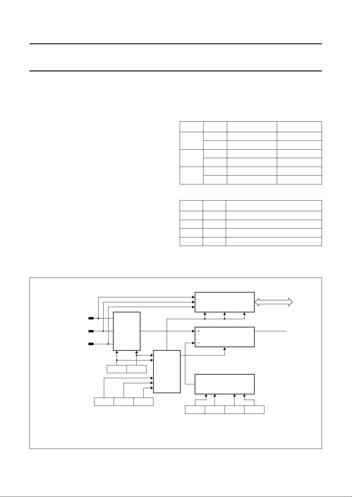
2 GENERAL DESCRIPTION
The PCA84C646 and PCA84C846 are 8-bit
microcontrollers with enhanced OSD and VST functions.
The PCA84C646 and PCA84C846 are members of the
PCA84C640 CMOS microcontroller family. They include
the PCF84CXXXA processor core, 6 or 8 kbytes of ROM
and 192 bytes of RAM.
I/O requirements are adequately catered for with
13 general purpose bidirectional I/O lines plus 16 function
combined I/O lines. One 14-bit PWM analog control,
3 AFC inputs (4-bit DAC + comparator) for VST and four
6-bit and 7-bit PWM analog control outputs are provided.
3 ORDERING INFORMATION
TYPE NUMBER
PCA84C646P
PCA84C846P
NAME DESCRIPTION VERSION
SDIP42 plastic shrink dual in-line package; 42 leads (600 mil) SOT270-1
PCA84C646; PCA84C846
In addition to all these features a master-slave I
interface, 2 directly testable lines and an enhanced OSD
facility for flexible screen format (maximum of 64 character
types) are also provided.
The on-chip Phase-Locked Loop (PLL) oscillator for OSD
operation considerably reduces the radiation generated by
the RC or LC oscillator. An 8-bit timer is integrated on-chip
with a 5-bit prescaler. Another 8-bit counter with
Schmitt-trigger input is used for clock/timer function
application.
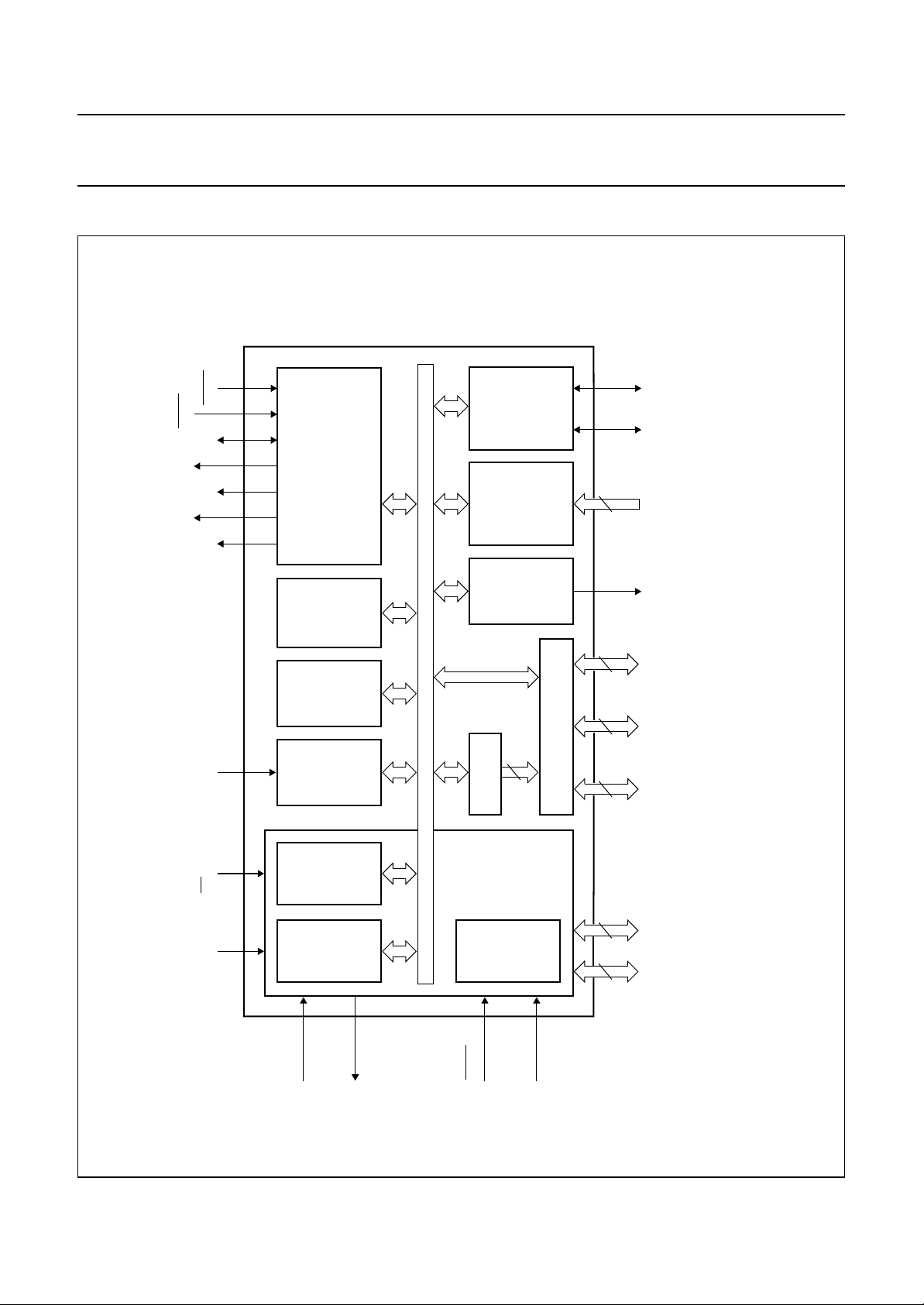
Figure 1 shows the block diagram of the PCA84C646 and
PCA84C846.
PACKAGE
2
C-bus
1995 Jun 15 4
Page 5
Philips Semiconductors Preliminary specification
Microcontrollers for TV tuning
control and OSD applications
4 BLOCK DIAGRAM
HSYNC
VSYNC
C
VOW2
VOW1
VOW0
VOB
ON SCREEN DISPLAY
8-bit internal bus
2
I C-BUS
AFC
3 x 4-BIT
PCA84C646; PCA84C846
MED169
INTERFACE
DAC +
COMPARATOR
SDA SCL
3
to
AFC2
INT / T0 T3
T1
RAM
192 bytes
(1)
(2)
ROM
6 kbytes or8 kbytes
8-BIT
COUNTER
CPU
8-BIT
EVENT
TIMER /
COUNTER
DAC
14-BIT
8
4 x 6-BIT PWM
4 x 7-BIT PWM
PCF84CXXXA
core excluding
ROM / RAM
I / O
PORTS
PARALLEL
48 4
8-BIT I/O PORTS
4
8
TDAC AFC0
DP20toDP23
DP10toDP13
to
DP00/PWM00
DP07/PWM07
P14
P10 to P12
P00toP07
Fig.1 Block diagram
XTAL1 (IN)
handbook, full pagewidth
XTAL2 (OUT)
1995 Jun 15 5
RESET
TEST / EMU
ROM size:
(1) 6 kbytes for PCA84C646.
(2) 8 kbytes for PCA84C846.
Page 6
Philips Semiconductors Preliminary specification
Microcontrollers for TV tuning
control and OSD applications
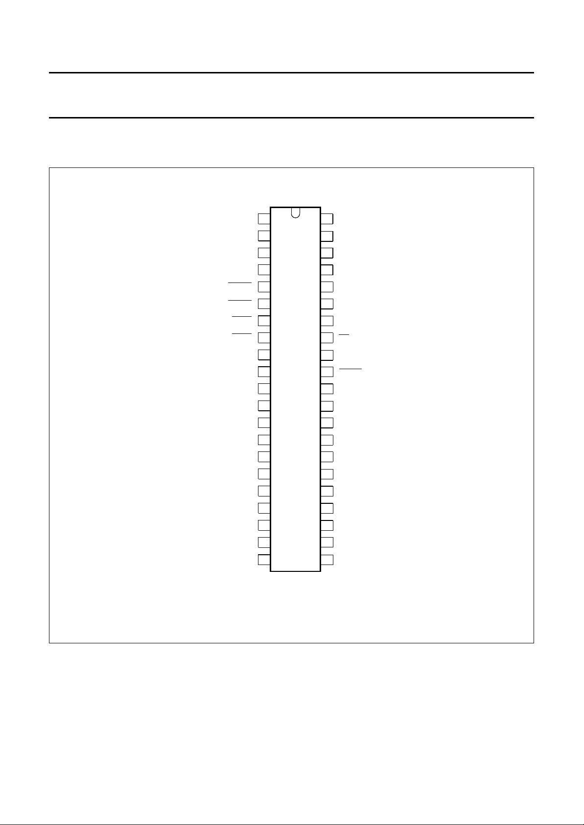
5 PINNING INFORMATION
5.1 Pinning
handbook, halfpage
DP22/VOW1
DP23/VOW0
VOB
VOW2
VSYNC
HSYNC
P10/DXWR
P11/DXRD
DP13/TDAC
P12/DXALE
T3
P14/DXINT
P00
P01
P02
P03
1
2
3
4
5
6
7
8
9
10
PCA84C646
11
PCA84C846
12
13
14
15
16
V
42
41
C
40
DP20/SDA
39
DP21/SCL
DP10/AFC0
38
37
DP11/AFC1
DP12/AFC2
36
35
INT/T0
34
T1
33
RESET
32
XTAL2
31
XTAL1
TEST/EMU
30
29
DP00/PWM00
28
DP01/PWM01
DP02/PWM02
27
PCA84C646; PCA84C846
DD
17
P04
18
P05
19
P06
20
P07
V
21
SS
Fig.2 Pin configuration PCA84C646P and PCA84C846P (SDIP42; SOT270-1).
1995 Jun 15 6
MED171
26
DP03/PWM03
25
DP04/PWM04
24
DP05/PWM05
23
DP06/PWM06
22
DP07/PWM07
Page 7
Philips Semiconductors Preliminary specification
Microcontrollers for TV tuning
PCA84C646; PCA84C846
control and OSD applications
5.2 Pin description
Table 1 Pin description for PCA84C646P and PCA84C846P; SDIP42 (see Fig.2)
SYMBOL PIN DESCRIPTION
VOB 1 Video fast blanking output signal.
VOW2 2 Video character outputs or derivative port lines.
DP22/VOW1 3
DP23/VOW0 4
VSYNC 5 Vertical synchronization signal input, active LOW.
HSYNC 6 Horizontal synchronization signal input, active LOW.
DXWR 7 Port line 10 or emulation DXWR signal input.
P10/
DXRD 8 Port line 11 or emulation DXRD signal input.
P11/
DP13/TDAC 9 Derivative I/O port or 14-bit D/A PWM.
P12/DXALE 10 Port line 12 or emulation DXALE signal input.
T3 11 Secondary 8-bit counter input pin (Schmitt-trigger).
P14/DXINT 12 Port line 14 or emulation DXINT signal input.
P00 to P07 13 to 20 General I/O port lines (10 mA).
V
SS
DP00/PWM00 to DP07/PWM07 29, 28, 27, 26,
TEST/EMU 30 Control input of testing and emulation mode, normally LOW.
XTAL1 31 Oscillator input terminal for system clock.
XTAL2 32 Oscillator output terminal for system clock.
RESET 33 Initialize input, active LOW.
T1 34 Direct testable pin and event counter input.
INT/T0 35 External interrupt/direct testable pin.
DP12/AFC2 36 Derivative I/O port or comparator input with 4-bit DAC.
DP11/AFC1 37
DP10/AFC0 38
DP21/SCL 39 Derivative port line or I
DP20/SDA 40 Derivative port line or I
C 41 External capacitor input for on chip PLL OSD oscillator.
V
DD
21 Ground.
Derivative I/O port;
25, 24, 23, 22
42 Power supply.
6-bit PWM (PWM04 to 07) or 7-bit PWM (PWM00 to 03).
2
C-bus clock line.
2
C-bus data line.
1995 Jun 15 7
Page 8
Philips Semiconductors Preliminary specification
Microcontrollers for TV tuning
control and OSD applications
6 RESET
The RESET pin is used as an active LOW input to initialize
the microcontroller to a defined state.
A Power-on-reset can be generated by using the
RC-circuit as shown in Fig.3.
An active reset can be generated by driving theRESET pin
from an external logic device. Such an active reset pulse
should not fall off before VDD has reached its
f
-dependent minimum operating voltage.
xtal
6.1 Reset trip level
RESET trip-voltage level is masked to 1.3 V in the
The
PCA84C646 and PCA84C846.
6.2 Reset status
• Derivative Registers status; for details see Table 40
• Program Counter: 00H
• Memory Bank: 00H
• Register Bank: 00H
• Stack Pointer: 00H
• All interrupts disabled
• Timer/event counter 1 stopped and cleared
• Timer prescaler modulo-32 (PS = 0)
• Timer flag cleared
• Serial I/O interface disabled (ESO = 0) and in slave
receiver mode
• Idle and Stop mode cleared.
PCA84C646; PCA84C846
7 ANALOG CONTROL
7.1 6 and 7-bit PWM outputs (PWM00 to PWM07)
The PCA84C646/PCA84C846 has eight PWM outputs for
analog controls of e.g. volume, balance, brightness and
saturation. These PWM outputs generate pulse patterns
with a repetition rate of
analog value is determined by the ratio of the HIGH-time
and the repetition time. A DC voltage proportional to the
PWM control setting is obtained by means of an external
integration network (low-pass filter).
The eight PWM outputs are specified as follows:
• PWM00 to PWM03 outputs with 7-bit resolution
• PWM04 to PWM07 outputs with 6-bit resolution.
Figure 4 shows the block diagram of the 6-bit or 7-bit PWM
DAC. The polarity of the PWM0n output is selected as
shown in Table 2 by the polarity control bit P6LVL/P7LVL
(Derivative Register 23; see Table 25).
The PWM0n output shares the pin with a DP0n I/O line
under control of a PWMnE enable bit; for selection see
Table 3.
Figure 5 shows the 6 and 7-bit PWM0n output patterns
(non-inverted; P6LVL/P7LVL = 0).
The HIGH-time of a PWM0n output is
t
= [PWMnDL]×t
HIGH
where:
[PWMnDL] = the contents of PWMn data latch
(n = 0 to 7; Derivative Register 10 to 17; see Table 40)
t0= 1/f
PWM
; f
PWM
1
⁄64× f
0
=1⁄3× f
xtal
PWM
.
or1⁄
128
× f
PWM
. The
V
DD
R
RESET
( 100 kΩ)
RESET
C
RESET
V
SS
(1) To avoid overload of the internal diode, an external
diode should be added in parallel if C
(1)
PCA84C646/846
RESET
internal reset
MED172
> 0.2 µF.
Fig.3 External components for RESET pin.
1995 Jun 15 8
Table 2 Polarity selection for the PWM0n output
P6L VL/P7LVL POLARITY
1 inverted
0 not inverted
Table 3 Selection of pin function: DP0n/PWM0n (note 1)
PWMnE FUNCTION
1 PWM0n output
0 DP0n I/O
Note
1. n = 0 to 7.
Page 9
Philips Semiconductors Preliminary specification
Microcontrollers for TV tuning
control and OSD applications
handbook, full pagewidth
f
PWM =
xtal
3
6 or 7-BIT PWM DATA LATCH
6 or 7-BIT DAC PWM
CONTROLLER
f
Q
Q
P6LVL/P7LVL
(1-BIT)
PCA84C646; PCA84C846
DP0n data
I/O
PWMnE
DP0n/PWM0n
MED177
f
handbook, full pagewidth
xtal
3
64
or
128
00
01
m
63
or
127
Fig.4 Block diagram of 6-bit or7-bit PWM DAC.
1 2 3 m m + 1 m + 2
decimal value PWM data latch
64
or
128
1
MLC261
Fig.5 Example PWM0n output patterns (P6LVL/P7LVL = 0).
1995 Jun 15 9
Page 10

Philips Semiconductors Preliminary specification
Microcontrollers for TV tuning
control and OSD applications
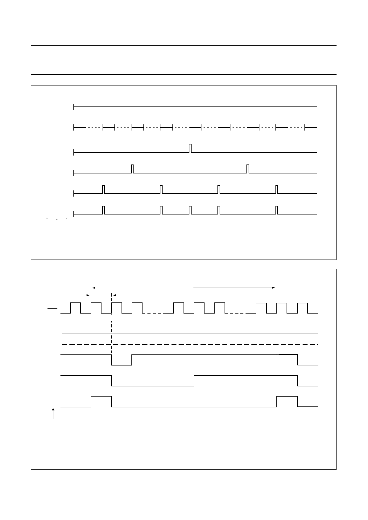
7.2 VST control 14-bit PWM DAC
The PCA84C646 and PCA84C846 have a PWM DAC
output (TDAC) with a resolution of 16384 levels for
Voltage Synthesized Tuning (VST).
Figure 6 shows the block diagram of the 14-bit PWM DAC
which consists of:
• Two 7-bit DAC interface latches (see Table 40):
– VSTH: Derivative Register 18; address 18H.
– VSTL: Derivative Register 19; address 19H.
• One 14-bit DAC data latch: VSTREG, which contents
defines the HIGH-time.
• 14-bit counter.
• Pulse control.
The contents of the interface latches VSTH and VSTL are
latched into VSTREG. The upper seven bits of VSTREG
are used for coarse adjustment, while the lower seven bits
are used for fine adjustment.
The contents of the interface latches VSTH and VSTL are
latched into VSTREG at the beginning of the first t
VSTL is written (see Fig.7). After VSTH and VSTL are
latched into VSTREG, it takes one t
to generate the
sub
appropriate pulse pattern.
Therefore, to ensure correct digital-to-analog conversion,
two t
periods should be allowed before beginning the
sub
next sequence (changing the contents of VSTH and
VSTL).
To ensure that the correct data is latched into VSTREG,
VSTH must contain the correct value before VSTL is
written; see the note in Fig.7.
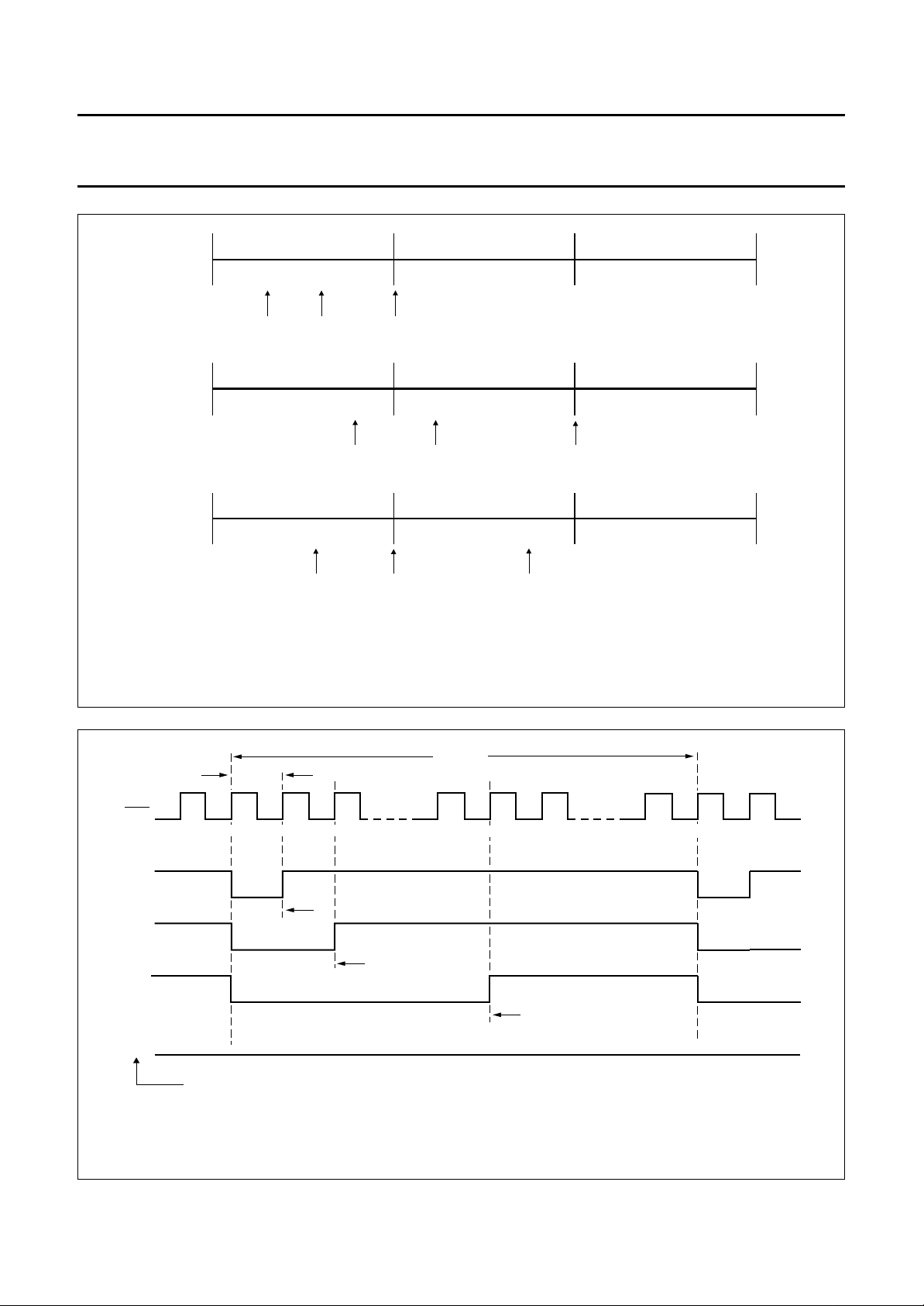
The repetition times of the pulse controllers are:
• Coarse, upper seven bits (VSTH):
t
sub
128 3 f
⁄×=
xtal
• Fine, lower seven bits (VSTL):
128 t
t
r
× 49152 f
sub
⁄==
xtal
Output TDAC shares the same pin as DP13; bit TDACE
(Derivative Register 22; see Table 22) selects the function
of pin DP13/TDAC.
Table 4 Selection of pin function DP13/TDAC
TDACE FUNCTION
1 TDAC; 14-bit PWM output
0 DP13
sub
after
PCA84C646; PCA84C846
7.2.1 C
An active HIGH pulse is generated in every subperiod; the
pulse width being determined by the contents of VSTH.
The coarse output (OUT1) is LOW at the start of each
subperiod and will remain LOW during
≤
t
s
Where ts is the time within t
The output will then go HIGH and remain HIGH until the
start of the next subperiod. The coarse pulse width may be
calculated as: .
7.2.2 F
Fine adjustment is achieved by generating an additional
pulse in specific subperiods. The pulse is added at the
start of the selected subperiod and has a pulse width of
3/f
xtal
subperiods a fine pulse will be added. It is the logic 0 state
of the value held in VSTL that actually selects the
subperiods. When more than one bit is a logic 0 then the
subperiods selected will be a combination of those
subperiods specified in Table 5. For example, if
VSTL = 111 1010 then this is a combination of:
• VSTL = 111 1110: subperiod 64 and
• VSTL = 111 1011: subperiods 16, 48, 80 and 112.
Pulses will be added in subperiods 16, 48, 64, 80 and 112.
This example is illustrated in Fig.9.
When VSTL holds 111 1111 fine adjustment is inhibited
and the TDAC output is determined only by the contents of
VSTH.
Table 5 Additional pulse distribution
111 1110 64
111 1101 32 and 96
111 1011 16, 48, 80 and 112
111 0111 8, 24, 40, 56, 72, 88, 104 and 120
110 1111 4, 12, 20, 28, 36, 44, 52...116 and 124
101 1111 2, 6, 10, 14, 18, 22, 26, 30...122 and 126
011 1111 1, 3, 5, 7, 9, 11, 13, 15, 17...125 and 127
OARSE ADJUSTMENT
VSTH 1+()3×
------------------------------------------f
xtal
.
subn
3
Pulse duration 127 VSTH–()
INE ADJUSTMENT
×=
-------f
xtal
. The contents of VSTL determine in which
VSTL ADDITIONAL PULSE IN SUBPERIOD
1995 Jun 15 10
Page 11
Philips Semiconductors Preliminary specification
Microcontrollers for TV tuning
control and OSD applications
‘MOVE instruction’
DAC INTERFACE
7-BIT DATA LATCH
(VSTH)
DATA LOAD
TIMING PULSE
Internal data bus
MSB LSB
DAC INTERFACE
7-BIT DATA LATCH
7
LOAD
(1)
COARSE 7-BIT
14-BIT DATA LATCH
(VSTREG)
7 7
PWM
OUT2OUT1
PCA84C646; PCA84C846
‘MOV instruction’
(VSTL)
7
FINE
ADDITIONAL
PULSE
GENERATOR
(1) See Fig.7 for timing.
PWM output polarity
control bit
P14LVL
ADD
Q
Q14 to 8 Q7 to 1
14-BIT COUNTER
Q
MED179
Fig.6 Block diagram of the 14-bit PWM DAC.
TDAC output
f = f
TDAC xtal
3
1995 Jun 15 11
Page 12
Philips Semiconductors Preliminary specification
Microcontrollers for TV tuning
control and OSD applications
t
CASE 1
CASE 2
CASE 3
sub
VSTH VSTL
t
sub
t
sub
VSTL
VSTH VSTL
t
sub
VSTH,VSTL is loaded into VSTREG
t
sub
t
sub
VSTH,VSTL is loaded VSTH
into VSTREG
PCA84C646; PCA84C846
t
sub
t
sub
VSTH,VSTL is loaded into VSTREG
t
sub
MED180
In CASE 1 and CASE 2, a new value for VSTH, VSTL is latched into VSTREG.
In CASE 3, VSTL, together with an old value of VSTH are latched into VSTREG.
Fig.7 Latching VSTH, VSTL into VSTREG.
handbook, full pagewidth
f
xtal
3
127 m m + 2
00
01
m
127
decimal value VSTH data latch
3/f
xtal
01
(1)
2 m + 1
(1)
t
subn
127 1
(1)
0
MGC573
(1) t
-------------------------------------------
s
f
xtal
VSTH 1+()3×
=
Fig.8 TDAC output (not inverted) with coarse adjustment only; VSTL = 1111111; P14LVL = 0.
1995 Jun 15 12
Page 13
Philips Semiconductors Preliminary specification
Microcontrollers for TV tuning
control and OSD applications
handbook, full pagewidth
111 1110
111 1101
111 1011
111 1010
VSTL
t
sub0
t
sub16
t
sub32
t
sub48
t
t
sub64
PCA84C646; PCA84C846
r
t
sub80
t
sub96
t
sub112
t
sub127
MCD314
handbook, full pagewidth
f
xtal
3
127 m
00
01
m
127
3/f
xtal
0
decimal value VSTH data latch
1
Fig.9 Fine adjustment output (OUT2).
t
sub16
2
m + 1
m + 2
127 1
0
MGC572
VSTL = 111 1010; Additional pulses in subperiods 16, 48, 64, 80 and 112.
Fig.10 Example of TDAC (not inverted) output pulses for several values of VSTH (t
1995 Jun 15 13
sub16
).
Page 14
Philips Semiconductors Preliminary specification
Microcontrollers for TV tuning
control and OSD applications
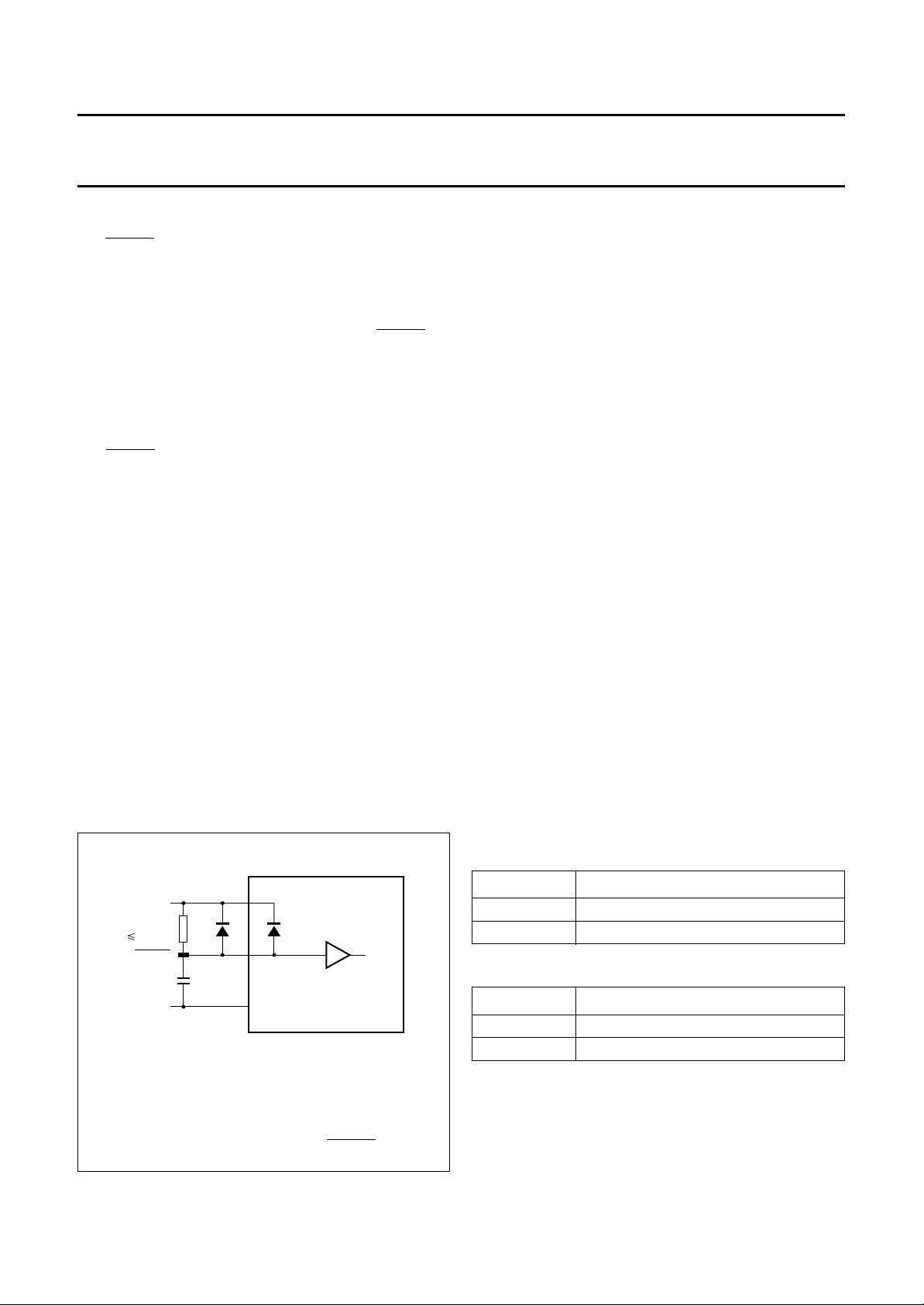
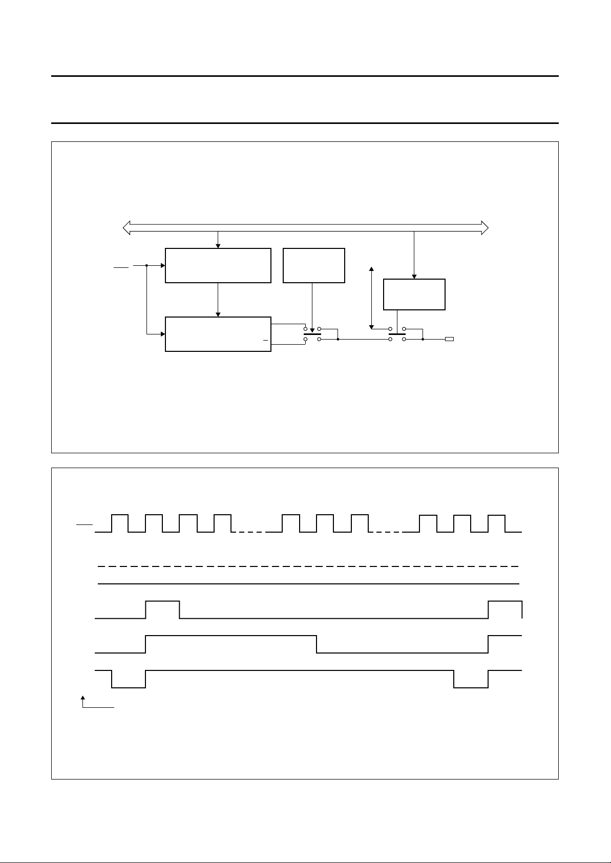
8 AFC INPUT
The AFC input is intended to measure the level of the
Automatic Frequency Control (AFC) signal. This is done
by comparing the AFC signal with the output of a 4-bit
digital-to-analog converter as shown in Fig.11. The DAC
analog switches select one of the 16 resistor taps that are
connected between VDD and VSS (controlled by bits
AFCV3, AFCV2, AFCV1, AFCV0; Derivative Register 20).
The AFCC signal (bit 0 in Derivative Register 20) then can
be tested to check whether the AFC input is higher or lower
than the DAC level.
The AFC inputs AFC0, AFC1 and AFC2 share the same
pins as Derivative Port lines DP10, DP11 and DP12. The
pin functions are selected by bits AFCE0, AFCE1, AFCE2
(AFC enable/disable bits; Derivative Register 22); for
selection see Table 6.
AFCH1 and AFCH0 (Derivative Register 20) select one
out of three AFC inputs to the comparator; for a correct
comparison, enable the corresponding AFC input (AFCi)
as shown in Table 7.
The conversion time of the AFC is greater than 6 µs but
less than 9 µs. It is recommended to add a NOP instruction
between the instruction which changes V
selection and the instruction which reads the AFCC bit
(compare bit).
or channel
ref
PCA84C646; PCA84C846
If the compare bit:
• AFCC = 0, then the AFC voltage < V
• AFCC = 1, then the AFC voltage > V
Table 6 Selection of pin function DP1i/AFCi (i = 0, 1, 2)
BIT VALUE PIN FUNCTION COMPARATOR
AFCE2 1 DP12 disabled
0 AFC2 enabled
AFCE1 1 DP11 disabled
0 AFC1 enabled
AFCE0 1 DP10 disabled
0 AFC0 enabled
Table 7 AFC input selection
AFCH1 AFCH0 SELECT
0 0 AFC Channel 0; AFC0
0 1 AFC Channel 1; AFC1
1 0 AFC Channel 2; AFC2
1 1 reserved
ref
ref
.
.
handbook, full pagewidth
DP10/AFC0
AFC
DP11/AFC1
DP12/AFC2
Channel selection
AFCE0 AFCE1 AFCE2
ANALOG
SELECTOR
AFCH1 AFCH0
AFC function enable
selection
ENABLE
SELECTOR
Fig.11 AFC circuit.
1995 Jun 15 14
AFCV3
(DP10 to DP12)
EN1 EN2EN0
COMPARATOR
EN
4-BIT D/A
AFCV2 AFCV1 AFCV0
AFC value selection
Internal bus
‘MOV A, D20’
instruction
to read AFCCx bit
MED185
Page 15
Philips Semiconductors Preliminary specification
Microcontrollers for TV tuning
control and OSD applications
Table 8 V
AFCV3 AFCV2 AFCV1 AFCV0 V
0000 V
0001 V
0010 V
0011 V
0100 V
0101 V
0110 V
0111 V
1000 V
1001 V
1010 V
1011 V
1100 V
1101 V
1110 V
1111 V
as a function of AFCV3 to AFCV0
ref
DD
DD
DD
DD
DD
DD
DD
DD
DD
DD
DD
DD
DD
DD
DD
ref
×1⁄
×2⁄
×3⁄
×4⁄
×5⁄
×6⁄
×7⁄
×8⁄
×9⁄
×10⁄
×11⁄
×12⁄
×13⁄
×14⁄
×15⁄
DD
PCA84C646; PCA84C846
V
(VDD= 5.0 V)
ref
16
16
16
16
16
16
16
16
16
16
16
16
16
16
16
0.31 V
0.62 V
0.93 V
1.25 V
1.56 V
1.87 V
2.18 V
2.50 V
2.81 V
3.12 V
3.43 V
3.75 V
4.06 V
4.37 V
4.68 V
5.00 V
1995 Jun 15 15
Page 16

Philips Semiconductors Preliminary specification
Microcontrollers for TV tuning
control and OSD applications
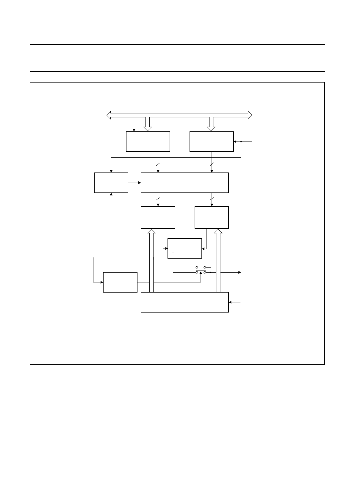
9 OSD (ON SCREEN DISPLAY) FUNCTION
9.1 Features
• Display RAM: 64 × 10 bit.
• Display character fonts: 64 (in which 62 customized +
2 special reserved codes).
• Display starting position (of the first character):
64 different positions by software control, both vertical
and horizontal.
• Character size: 4 different character sizes, line-by-line
basis, 1 dot = 1H/1V, 2H/2V, 3H/3V, 4H/4V.
• Character matrix: 12 × 18 with no spacing between
characters.
• Foreground colours: 8, combination of Red, Green, Blue;
character-by-character basis.
• Background/shadowing modes: 4, No background,
Box shadowing, North-west shadowing,
Frame shadowing (raster blanking), frame basis.
• Background colours: 8, combination of Red, Green,
Blue; word-by-word basis. Available when background
mode is either in Box shadowing or North-west
shadowing and Frame shadowing mode.
• On-chip OSD oscillator.
• Character blinking rate: 1 : 1, 1 : 3, 3 : 1 (frequency:
1
⁄16,1⁄32,1⁄64 or1⁄
e.g. NTSC:60⁄16Hz, PAL:50⁄64Hz etc.); character basis.
• Display format: flexible display format by using Carriage
Return (CR) code, maximum number of characters per
line is flexible and depending on the OSD clock.
• Spacing between lines: 4 different choices from 0, 4,
8 or 12 horizontal scan lines.
• Display character RAM auto-address-post-increment
when writing data.
• Programmable HSYNC and VSYNC active input polarity.
• Programmable G (VOW1), B (VOW2), R (VOW0) and
FB (VOB) output polarity.
9.2 Horizontal display position control
The horizontal position counter is increased every OSD
clock (f
) cycle after the programmed level of HSYNC
OSD
occurs at the HSYNC pin and is reset when the opposite
polarity of the HSYNC is reached. Horizontal start position
is controlled by Derivative Register 36 (HPOS;
see Table 36). The starting position is calculated as:
HP = [4 × (H5 to H0) + 5] × (OSD clock cycle)
where (H5 to H0) = decimal value of register HPOS;
(H5 to H0) ≥ 10.
128
of f
, programmable,
VSYNC
PCA84C646; PCA84C846
9.3 Vertical display position control
The vertical position counter is increased every HSYNC
cycle and is reset by the VSYNC signal. Vertical start
position is controlled by Derivative Register 35 (VPOS;
see Table 34). The vertical starting position is calculated
as:
VP = [4 × (V5 to V0)] × (horizontal scan lines)
where (V5 to V0) = decimal value of register VPOS;
(V5 to V0) ≥ 0.
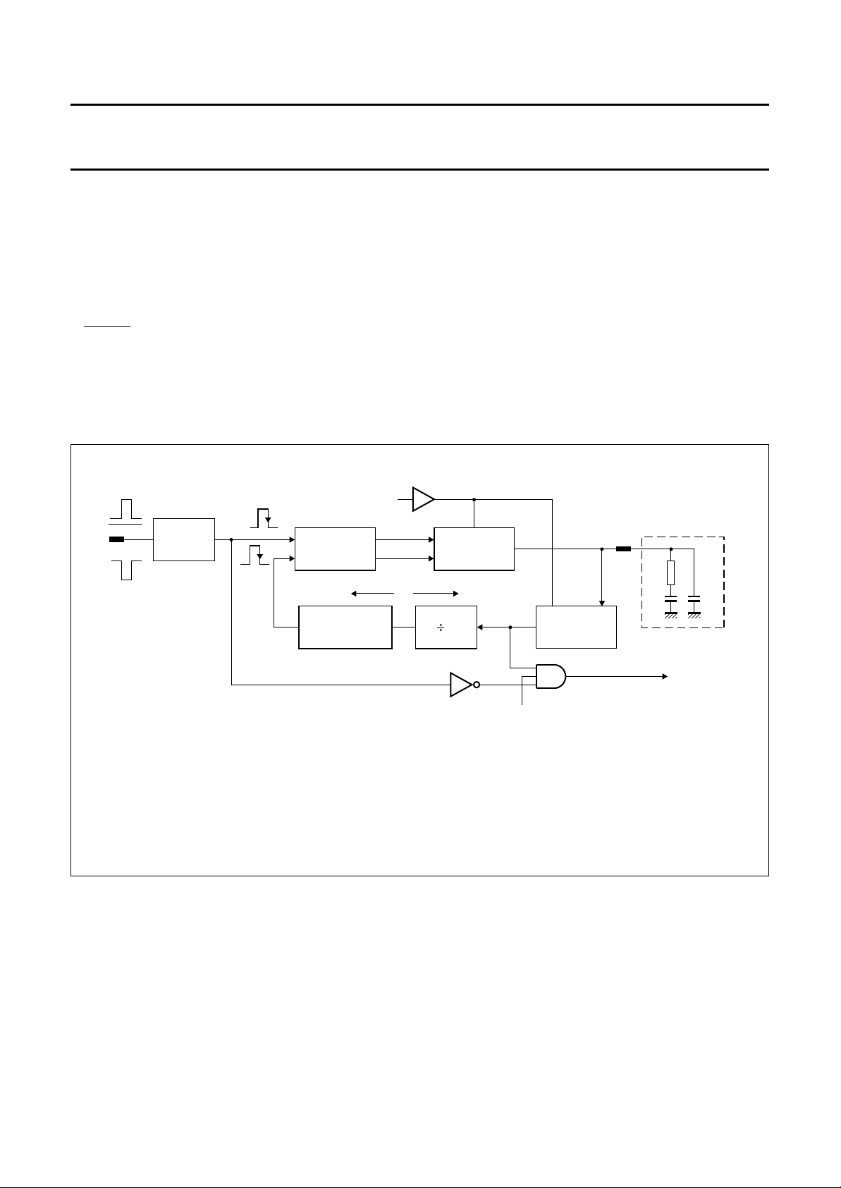
9.4 Clock generator
Figure 12 illustrates the block diagram of the on-chip OSD
clock generator which consists of a Phased-Lock Loop
(PLL) circuit. The Voltage Controlled Oscillator (VCO)
outputs a clock (f
8 to 20 MHz (see Fig.12). The input signal f1= HSYNC.
The programmable active level detector:
• Passes signal f1, when HSYNC is active HIGH, or
• Inverts signal f1, when HSYNC is active LOW.
The output signal f2 is always active HIGH. The VCO is
synchronized with the HIGH-to-LOW edge of the f2 signal.
The value programmed in the 7-bit PLL Programmable
Counter control register (PLLCN; Derivative Register 25;
see Table 40) determines:
f
VCO=f1
×16 × (decimal value of 7-bit counter);
where 16< (decimal value of 7-bit counter) < 48.
The value 16 is the 4-bit prescaler which increases or
decreases the output of the VCO in steps of (16 × f1).
Given an example of f1= 15.750 kHz, the f
increased or decreased in steps of
16 × 15.750 kHz = 252 kHz = 0.25 MHz.
The f
is fed into a buffer to generate the OSD dot clock
VCO
frequency signal (f
Decreasing f
OSD
Recommended: 4 MHz ≤ f
The OSD clock is enabled/disabled by the state of the EN
bit (Derivative Register 34; see also Section 12.4). When
the OSD clock is disabled (f
remains active, therefore the transient time from the OSD
clock start-up to locking into the external HSYNC signal is
reduced.
As the on-chip oscillator is always active after Power-on,
when the OSD clock is enabled no large currents flow (as
for RC or LC oscillators) and therefore radiated noise is
dramatically reduced.
) with a frequency range of
VCO
); 4 MHz ≤ f
OSD
OSD
≤ 12 MHz.
gives broader characters.
typical ≤ 12 MHz.
OSD
= LOW) the oscillator
OSD
VCO
is then
1995 Jun 15 16
Page 17
Philips Semiconductors Preliminary specification
Microcontrollers for TV tuning
control and OSD applications
9.4.1 MOUNTING PRECAUTIONS
To achieve good OSD performance, take the following
precautions for the microcontroller mounting:
• Apply the recommended R, Cs and Cp (PLL loop filter)
values as shown in Fig.12 and place them as close as
possible to pin C (41).
• To guarantee stable PLL operation, apply a noise-free
HSYNC signal (pin 6).
• Avoid heavy loading of the output pins.
• The supply voltage (VDD) must be correctly decoupled.
Connect decoupling capacitors as close as possible to
the VDD and VSS pins.
handbook, full pagewidth
f
1
HSYNC
ACTIVE
LEVEL
DETECTOR
f
2
FREQUENCY
(2)
PROGRAMMABLE
STANDBY
PHASE/
DETECTOR
divided by N
7-BIT COUNTER
PCA84C646; PCA84C846
• Position microcontroller optimal and away from
components bearing high voltage and/or strong current.
• PLL loop filter ground of capacitors C
directly connected to the VSS pin (21). Avoid a ground
loop and separate the ground from other digital signals
ground.
• The connection between VSS pin (21) and +5 V regulator
ground/switching power supply secondary ground must
be as short as possible.
CHARGE PUMP
AND
LOOP FILTER
f
16
VCO
VOLTAGE
CONTROLLED
OSCILLATOR
C
and Cp must be
s
(1)
R
C
s
C
p
f
OSD
(OSD clock)
(1) R=10to47kΩ; typ. 15 kΩ.
= 100 to 470 nF; typ. 220 nF.
C
s
=1⁄10Cs.
C
p
For mounting see Section 9.4.1 “Mounting precautions”.
(2) Example:
= 15.750 kHz and (decimal value of 7-bit counter) = 32 then f
If f
1
and the output of the Programmable 7-bit counter is 15.750 kHz.
VCO
Fig.12 On-chip OSD oscillator.
1995 Jun 15 17
= 8.064 MHz
OSD disable
MED196
Page 18
Philips Semiconductors Preliminary specification
Microcontrollers for TV tuning
control and OSD applications
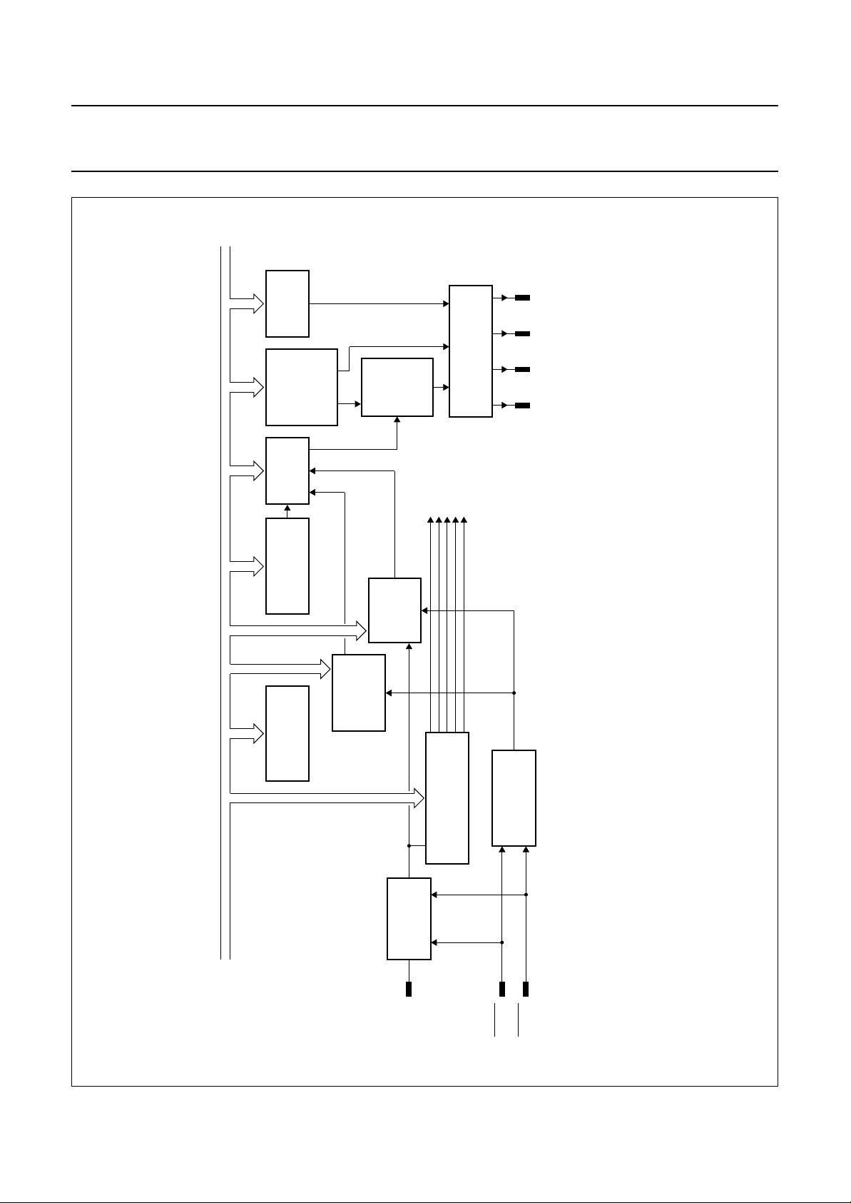
CONTROL
REGISTER
RAM
DISPLAY
CHARACTER
BUFFER
ADDRESS
SELECTOR
BIT
DISPLAY
PATTERN
DISPLAY CONTROL
ROM(64)
control
signals
PCA84C646; PCA84C846
MED189
AND
OUTPUT STAGE
RGBFB
VOW1 VOW0 VOW2 VOB
CPU bus
COUNTER
WRITE ADDRESS
POSITION
HORIZONTAL
CONTROL
CHARACTER SIZE
POSITION
VERTICAL
REGISTER/
COUNTER
REGISTER/
ON-CHIP
C
COUNTER
CONTROL REGISTER
INSTRUCTION DECODER
OSCILLATOR
CIRCUIT
INTERNAL
SYNCHRONOUS
handbook, full pagewidth
Fig.13 OSD block diagram.
1995 Jun 15 18
HSYNC
VSYNC
Page 19
Philips Semiconductors Preliminary specification
Microcontrollers for TV tuning
PCA84C646; PCA84C846
control and OSD applications
10 DISPLAY RAM ORGANIZATION
The display RAM is organized as 64 × 10 bits.
The general format of each RAM location is as follows:
• Bits <9-4> hold data, comprising:
– Customer designed Character Font Codes (62)
– Carriage Return Code (1)
– Space Code (1).
• Bits <3-0> contain the attributes of the Character Font:
– Foreground colour and Blinking
– Character size and Line space
– Background colour and End-of-Display .
Table 9 Format of Character Font Code
987654321 0
C5 C4 C3 C2 C1 C0 T3 T2 T1 T0
Character Font Code (00H - 3DH) Foreground colour Blink
10.1 Description of display RAM codes
There are three data formats for the display RAM code
1. Character Font Code
2. Carriage Return Code
3. Space Code.
The three data formats and their descriptions are shown in
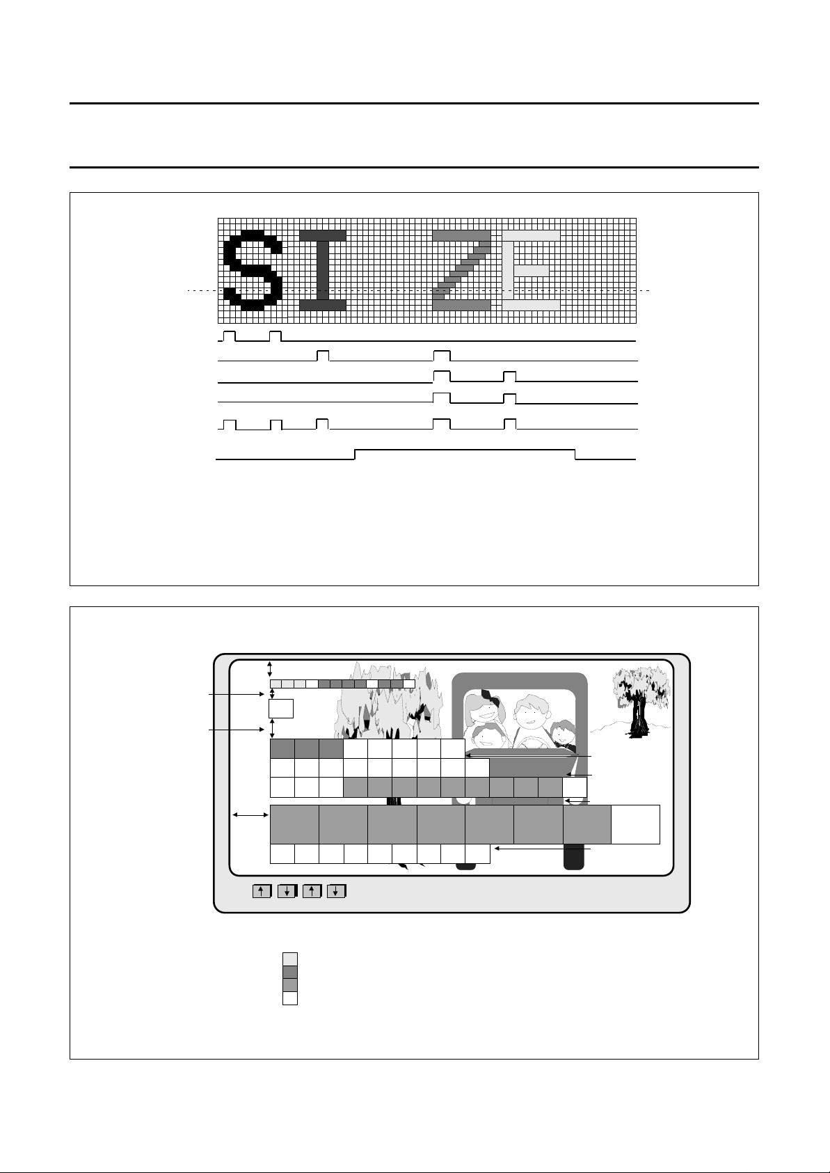
Tables 9 to 17. Figure 14 illustrates an example of the
timing of FB, R, G, and B pulses when displaying a line of
dots stream in a character.
FB = VOB; R = VOW0, G = VOW1; B = VOW2.
Figure 15 shows an example of the screen which includes
some Cariage Return and Space codes.
Table 10 Description of Character Font Code bits
SYMBOL DESCRIPTION
C5 to C0 If bits <9-4> are in the range (00H to 3DH), then this is a Character Font Code and 1 from 62 customer
designed character fonts can be selected.
T3 to T1 Bits <3-1> determine the (Foreground) colour (1 out of 8) of this character; see Table 11.
T0 Blinking of this character is controlled by bit <0>. See Section 12.3 for duty cycle and frequency control.
When T0 = 0; blinking is OFF.
When T0 = 1; blinking is ON. Blinking rate:
Table 11 Selection of Background and Foreground colour
T3
(RED)
0 0 0 black
0 0 1 blue
0 1 0 green
0 1 1 cyan
100red
1 0 1 magenta
1 1 0 yellow
1 1 1 white
T2
(GREEN)
1
⁄16,1⁄
32
,1
⁄64or1⁄
128
T1
(BLUE)
× f
VSYNC
.
COLOUR
1995 Jun 15 19
Page 20
Philips Semiconductors Preliminary specification
Microcontrollers for TV tuning
PCA84C646; PCA84C846
control and OSD applications
Table 12 Format of Carriage Return Code
9876543210
C5 C4 C3 C2 C1 C0 T3 T2 T1 T0
Carriage Return Code (3EH) Character size Line Spacing
Table 13 Description of Carriage Return Code bits; format is shown in Table 12
SYMBOL DESCRIPTION
C5 to C0 If bits <9-4> hold 3EH, then this is the Carriage Return Code. The current display line is terminated
(a transparent pattern appears on the screen) and the next character will be displayed at the beginning of
the next line.
T3 to T2 Bits <3-2> select the size of the of the character to be displayed on the next line; see Table 14.
T1 to T0 Bits <1-0> determine the spacing between lines of displayed characters. Spacing is a multiple of the
number of horizontal scan lines. In order to prevent vertical jumping of the display, the first line should be
a non-displayed line i.e. the Carriage Return Code.
The line spacing for this code must not be zero; see Table 15.
Table 14 Selection of character size
T3 T2 CHARACTER DOT SIZE
0 0 1H/1V
0 1 2H/2V
1 0 3H/3V
1 1 4H/4V
(1)
Table 15 Selection of line spacing
T1 T0 LINE SPACING
0 0 0H line
0 1 4H line
1 0 8H line
1 1 12H line
Note
1. H is the OSD clock period; V is the number of
horizontal scan lines per dot.
Table 16 Format of Space Code
987654321 0
C5 C4 C3 C2 C1 C0 T3 T2 T1 T0
Space Code (3FH) Background colour End
Table 17 Description of Space Code bits; format is shown in Table 16
SYMBOL DESCRIPTION
C5 to C0 If bits <9-4> hold 3FH, then this is the Space Code. A transparent pattern, equal to one character width,
will be displayed on the screen.
T3 to T1 Bits <3-1> determine the background colour of the characters including the Space Code in Box
shadowing mode but following the Space Code in North-west shadowing mode. See Section 12.4 for
more details. Background colour selection is the same as Foreground colour selection; see Table 11.
T0 Bit <0> is the End-of-Display bit and indicates the end of display of the current screen before exhaustion
of display RAM. The last character displayed on the TV screen is either the 64
Code with the End-of-display attribute set to logic 1.
When T0 = 0; continue display of next character.
When T0 = 1; end of display.
th
RAM location or a Space
1995 Jun 15 20
Page 21
Philips Semiconductors Preliminary specification
Microcontrollers for TV tuning
control and OSD applications
handbook, full pagewidth
R
G
B
I
FB
ACM
"S" : red colour "E" : B+I colour
"I" : green colour 1st SP code : ACM = on
"Z" : G+B+I colour 2nd SP code : ACM = off
PCA84C646; PCA84C846
SP code SP code
MED204
handbook, full pagewidth
line spacing 1 = 4H
line spacing 2 = 8H
Fig.14 R, G, B and FB timing.
Vstart
HI ! THIS ISSP SP CR
CR
T H E N E W
F U N C I O NT
I N P C F 8 5 C X X
Hstart
St andal
SP
Volume
Four different background colours (in box shadowing mode):
Channel
Black
Red
Green
Blue
SP
SP
E L C O M EW
CR
CR
CR
X
line spacing 3 = 0H
line spacing 4 = 0H
CR
line spacing 4 = 4H
line spacing 6 = 0H
CR
MED205
Fig.15 On-screen-display (an example).
1995 Jun 15 21
Page 22
Philips Semiconductors Preliminary specification
Microcontrollers for TV tuning
control and OSD applications
10.2 Loading character data into display RAM
Three Derivative Registers are used to address and load
data into the display RAM. These registers (configurations
are shown in Tables 18, 19 and 20) are described in the
following Sections.
10.2.1 DCR A
Table 18 DCRAR (address 30H)
76543210
−−A5 A4 A3 A2 A1 A0
This is Derivative Register 30 and bits <5-0> holds the
address of the location in display RAM to which the data
held in registers DCRTR and DCRCR will be written to.
Bits <7-6> are reserved.
10.2.2 DCR A
Table 19 DCRTR (address 31H)
76543210
−−−−T3 T2 T1 T0
DDRESS REGISTER (DCRAR)
TTRIBUTE REGISTER (DCRTR)
PCA84C646; PCA84C846
2. Load the character attributes into DCRTR. If the
attributes of a series of displayed characters are the
same, only DCRCR needs to be updated.
The meaning of the attributes (4 bits) is dependent on
the contents of the next command (the data in the
DCRCR bits <5-0>; i.e. Carriage Return Code, Space
Code or Character Font Code).
3. Load the character data into DCRCR. This operation
loads the selected RAM location with the data held in
registers DCRTR and DCRCR. The address held in
DCRAR is then incremented by ‘1’ pointing to the next
RAM location in anticipation of the next operation.
Overflow of the DCRAR, i.e. overflow from 63 to 64,
makes it reset to zero. After the instruction ‘MOV D32H, A’
is finished, the post-increment operation is performed
automatically. Auto-post-increment operation:
Begin
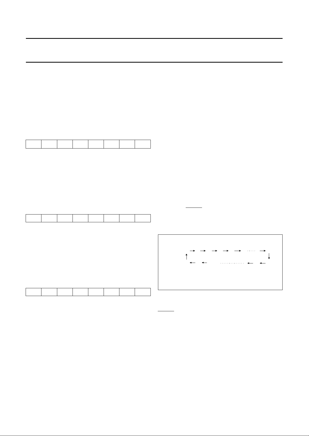
(DCRAR) ≤ (DCRAR) + 1
If (DCRAR) > 63 then (DCRAR) ≤ 0
End
After master RESET the initial values of DCRAR, DCRTR
and DCRCR are all zero. Figure 16 shows how DCRAR is
incremented and advanced.
This is Derivative Register 31 and holds the character font
attribute data. The data will be loaded into bits <3-0> of the
location in RAM pointed to by the contents of DCRAR.
Bits <7-4> are reserved.
10.2.3 DCR C
HARACTER REGISTER (DCRCR)
Table 20 DCRCR (address 32H)
76543210
−−C5 C4 C3 C2 C1 C0
This is Derivative Register 32 and holds the character data
that will be loaded into bits <9-4> of the location in RAM
addressed by the contents of DCRAR. Bits <7-6> are
reserved.
10.3 Writing character data to display RAM
1. Select the start address in display RAM. The start
address is stored in DCRAR and can take any value
between 0 and 63.
handbook, halfpage
DCRAR
616263 1819
1700 01 02 03 04
MED208
Fig.16 DCRAR increment cycle.
10.4 Default value of the display character
The default values of the display characters, after master
RESET, are as follows:
• Background colour = Blue (R = 0, G = 0, B = 1)
• Character size = 1V/1H
• End-of-Display control bit = 0.
If another set-up is needed, the first character should be
SP code and second character is CR code to define the
character size and background colour.
1995 Jun 15 22
Page 23

Philips Semiconductors Preliminary specification
Microcontrollers for TV tuning
control and OSD applications
11 CHARACTER ROM
Each character font is stored in the on-chip character ROM
in a 12 × 19 dot matrix. However, only elements in Rows 1
to 18 (12 × 18 dot matrix) can be selected as visible dots
on the screen.
Row 0 is only used for the combination of two characters
in a vertical direction when North-west shadowing mode is
selected (for details see Section 12.4). Row 0 contains the
same bit pattern of Row 18 of the character above it. If no
combined character in vertical direction is intended for this
character, Row 0 should be filled with all zeros.
11.1 Character ROM organization
ROM is divided into two parts: ROM1 and ROM2. The
organization of the bit patterns stored in ROM1 and ROM2
and the file format to submit to Philips for customized
character sets is shown in Fig.17.
A software package (OSDGEM) that assists in the design
of character fonts on-screen and that also automatically
PCA84C646; PCA84C846
generates the bit pattern HEX files is available on request.
The package is run under the MS-DOS environment for
IBM compatible PCs.
Regarding Fig.17 the following points should be noted.
1. Row 0 of each font is reserved for vertical combination
of two fonts.
2. Binary 1 denotes visual dots.
3. ROM1 and ROM2 data files are in INTEL hex format
on a byte basis. Each byte is structured High nibble
followed by Low nibble.
4. The unused last byte of each font in ROM1 must be
filled with FFH.
1
5. The unused last 2
the same data as held in the corresponding address in
ROM1.
6. The data bytes of the last 2 reserved fonts (Carriage
Return and Space Codes) should be filled with 00H.
7. CS denotes Checksum.
⁄2bytes in ROM2 must be filled with
handbook, full pagewidth
MSB
Column
11 10 9 8 7 6 5 4 3 2 1 0
0
1
2
3
4
5
6
ROW
7
8
9
10
11
12
13
14
15
16
17
18
ROM1
: 1 0 0 0 0 0 0 0 00 00 22 FC 03 22 20 F2 3F 01 20 55 0C 00 03
: 1 0 0 0 1 0 0 0 < - - - DATA FOR FONT 2 - - - 12 34>
: 1 0 0 0 2 0 0 0 < - - - DATA FOR FONT 3 - - - 56 78>
byte #
0 1 2 3 4 5 6 7 8 9 A B C D E F
__ __ __ __ __ __ __ __ __ __ __ __ __ __ __
LSB
ROM2
: 1 0 0 0 0 0 0 0 FC 03 22 20 C2 3F 20 12 00 53 65 00 58
: 1 0 0 0 1 0 0 0 < - - - DATA FOR FONT 2 - - - >
: 1 0 0 0 2 0 0 0 < - - - DATA FOR FONT 3 - - - >
0 0 0
3 F C
2 2 0
2 2 0
3 F C
2 2 0
2 2 0
3 F C
2 2 0
2 2 0
3 F F
0 0 1
0 0 1
5 5 3
5 5 2
0 0 6
0 0 C
0 5 8
0 3 0
ROM1
ROM2
ROM1
ROM2
ROM1
ROM2
ROM1
ROM2
ROM1
ROM2
ROM1
ROM2
ROM1
ROM2
ROM1
ROM2
ROM1
ROM2
ROM1
ROM1 ROM2
0 0 0
2 2 0
3 F C
2 2 0
2 2 0
3 F F
0 0 1
5 5 2
0 0 C
0 3 0
F F
F F
F F
>
>
>
0 0 03 FF
1 X 34 FF
5 X 78 FF
MLB760
3 F C
2 2 0
2 2 0
3 F C
2 2 0
0 0 1
5 5 3
0 0 6
0 5 8
CS
CS
CS
CS
CS
CS
Fig.17 Font pattern stored in character ROM1 and ROM2.
1995 Jun 15 23
Page 24

Philips Semiconductors Preliminary specification
Microcontrollers for TV tuning
PCA84C646; PCA84C846
control and OSD applications
12 OSD CONTROL REGISTERS
The functions of the OSD circuitry are controlled by the Derivative Registers as shown in Table 21.
Table 21 OSD Control Registers overview
NAME
CON1 22 22H Enable TDAC; the I
CON2 23 23H Selects the output polarity of the PWM outputs and also enables and selects the
CON3 33 33H Selects the blinking frequency and the active ratio of the blinking frequency for the
CON4 34 34H Selects the 4 display modes; the active state of
VPOS 35 35H Selects the vertical starting position of the display row.
HPOS 36 36H Selects the horizontal starting position of the display row.
BCC 37 37H Selects the background colour.
DERIVATIVE REGISTER
NUMBER ADDR
FUNCTION
2
C-bus lines; the AFC functions and the VOW0 and VOW1
lines.
VSYNC interrupt.
OSD.
HSYNC and VSYNC and the
output polarity of the FB and VOW0 to VOW2 outputs. It also enables/disables the
OSD clock.
1995 Jun 15 24
Page 25

Philips Semiconductors Preliminary specification
Microcontrollers for TV tuning
PCA84C646; PCA84C846
control and OSD applications
12.1 Derivative Register 22 (CON1)
Table 22 Derivative Register 22 (address 22H)
76543210
TDACE SCLE SDAE ADC2E ADC1E ADC0E VOW1E VOW0E
Table 23 Description of Derivative Register 22 bits
BIT SYMBOL DESCRIPTION
7 TDACE Pulse Width Modulated output TDAC enable bit. When:
TDACE = 1; pin DP13/TDAC is selected as output TDAC.
TDACE = 0; pin DP13/TDAC is selected as Derivative Port line DP1.
2
6 SCLE I
5 SDAE I2C-bus data enable bit. When:
4 AFCE2 These 3 bits select the pin function of DP1i/AFC and enable/disable the comparator in
3 AFCE1
2 AFCE0
1 VOW1E Pin function selection bit. When:
0 VOW0E Pin function selection bit. When:
C-bus clock enable bit. When:
2
SCLE = 1; pin DP21/SCL is selected as SCL (I
SCLE = 0; pin DP21/SCL is selected as Derivative Port line DP21.
SDAE = 1; pin DP20/SDA is selected as SDA (I
SDAE = 0; pin DP20/SDA is selected as Derivative Port line DP20.
the AFC circuit; for the selection and enable/disable function see Table 7.
VOW1E = 1; pin DP22/VOW1 is selected as VOW1.
VOW1E = 0; pin DP22/VOW1 is selected as Derivative Port line DP22.
VOW0E = 1; pin DP23/VOW1 is selected as VOW1.
VOW0E = 0; pin DP23/VOW1 is selected as Derivative Port line DP23.
C-bus clock line).
2
C-bus data line).
1995 Jun 15 25
Page 26

Philips Semiconductors Preliminary specification
Microcontrollers for TV tuning
PCA84C646; PCA84C846
control and OSD applications
12.2 Derivative Register 23 (CON2)
Table 24 Derivative Register 23
76543210
VINT VIEN −−−P14LVL P7LVL P6LVL
Table 25 Description of Derivative Register 23 bits
BIT SYMBOL DESCRIPTION
7 VINT Bit VINT indicates if the interrupt comes from
I2C-bus when the CPU gets interrupted by interrupt vector address 7.
6 VIEN The
5to4 − These three bits are reserved.
2 P14LVL Polarity select bit for output TDA. When:
1 P7LVL Polarity select bit for outputs PWM00 to PWM03. When:
0 P6LVL Polarity select bit for outputs PWM04 to PWM07. When:
VSYNC leading edge (active level detection automatically done by the
PCA84C646/PCA84C846) generates an interrupt if bit VIEN = 1 and the SIO interrupt is
enabled (i.e. the I2C-bus and the VSYNC interrupt shares the same interrupt vector).
P14LVL = 1; the TDAC output is inverted.
P14LVL = 0; the TDAC output is not inverted.
P7LVL = 1; the outputs PWM00 to PWM03 are inverted.
P7LVL = 0; the outputs PWM00 to PWM03 are not inverted.
P6LVL = 1; the outputs PWM04 to PWM07 are inverted.
P6LVL = 0; the outputs PWM04 to PWM07 are not inverted.
VSYNC (if VINT = 1 and VIEN = 1) or
1995 Jun 15 26
Page 27

Philips Semiconductors Preliminary specification
Microcontrollers for TV tuning
PCA84C646; PCA84C846
control and OSD applications
12.3 Derivative Register 33 (CON3)
Derivative Register 33 is to control the character blinking related operation. Figure 18 shows the timing diagram of
character blinking frequency and blinking ratio.
Table 26 Derivative Register 33
76543210
−−−−BR1 BR0 BF1 BF0
Table 27 Description of Derivative Register 33 bits
BIT SYMBOL DESCRIPTION
7 to 4 − These 4 bits are reserved.
3 BR1 Blinking active ratio select bits. These two bits allow one from a choice of three active
2 BR0
1 BF1
0 BF0
blinking ratios to be selected; see Table 28.
Blinking frequency select bits. These two bits allow one from a choice of four blinking
frequencies to be selected.
f
Blinking frequency
where ‘2
(BF1, BF0)
VSYNC
---------------------------------------16 2
BF1, BF0()
×
’ is a decimal value determined by bits BF1 and BF0; see Table 29.
Hz=
,
Table 28 Active ratio determined by bits BR1 and BR0
BR1 BR0 ACTIVE RATIO
0 0 3 : 1 (default)
0 1 1:1
1 0 1:3
1 1 reserved
handbook, full pagewidth
Blinking frequency:
Blinking ratio: 1 : 3
Blinking frequency:
Blinking ratio: 1 : 1
Blinking frequency:
Blinking ratio: 3 : 1
Blinking frequency:
Blinking ratio: 1 : 3
Blinking frequency:
Blinking ratio: 1 : 1
Blinking frequency:
Blinking ratio: 3 : 1
VSYNC
f
VSYNC
16
f
VSYNC
16
f
VSYNC
16
f
VSYNC
32
f
VSYNC
32
f
VSYNC
32
60 Hz
0123 78 1011
Table 29 Blinking frequency determined by (BF1,BF0)
60 Hz
(BF1, BF0)
BLINKING FREQUENCY (Hz)
1
⁄16× f
VSYNC
1
⁄32× f
VSYNC
1
⁄64× f
VSYNC
1
⁄
128
× f
VSYNC
(default)
14 15
MRA848
BF1 BF0 2
00 1
01 2
10 4
11 8
14 15 0123 78 1011
Fig.18 Example of character blinking (NTSC 525LPF/60Hz).
1995 Jun 15 27
Page 28

Philips Semiconductors Preliminary specification
Microcontrollers for TV tuning
PCA84C646; PCA84C846
control and OSD applications
12.4 Derivative Register 34 (CON4)
This register selects the 4 display modes(Mode 0 to Mode 3); the active state of HSYNC and VSYNC and the output
polarity of the FB and VOW0 to VOW2 outputs. It also enables/disables the OSD clock (f
Table 30 Derivative Register 34
76543210
−−S1 S0 Hp Vp Bp EN
Table 31 Description of Derivative Register 34 bits
BIT SYMBOL DESCRIPTION
7 − These two bits are reserved.
6 −
5 S1 Display mode select bits; see Table 32.
4S0
3Hp
2Vp
1 Bp Output polarity control bit for FB, VOW0, VOW1 and VOW2 (see Fig.20).
0 EN OSD clock enable/disable bit.
HSYNC signal polarity control bit (see Fig.19).
When Hp = 1; the active level of
When Hp = 0; the active level of
VSYNC signal polarity control bit (see Fig.19).
When Vp = 1; the active level of
When Vp = 0; the active level of
When Bp = 1; the polarity of FB, VOW0, VOW1 and VOW2 is HIGH (default state).
When Bp = 0; the polarity of FB, VOW0, VOW1 and VOW2 is LOW.
When EN = 1; the OSD clock is enabled.
When EN = 0; the OSD clock is disabled.
HSYNC is HIGH.
HSYNC is LOW (default state).
VSYNC is HIGH.
VSYNC is LOW (default state).
OSD
).
Table 32 Selection of Display Modes
S1 S0 DISPLAY MODE
0 0 Mode 0 No background mode (see Fig.21). The OSD fonts/characters are directly superimposed on
the TV video signals.
0 1 Mode 1 North-west shadowing mode (see Fig.22). Available only in the character size 2V/2H or 4V/4H
(V: horizontal line; H: OSD clock).The shadows of the characters are generated by placing a
light source on the North-west 45 degree direction (see also Figs 25 and 26). When designing
the character bit pattern, care must be taken that the shadows generated by this mode is only
within the cell boundary in vertical direction (see Figs 28 and 29 for details). But shadows
generated by this mode in horizontal direction has no boundary limitation (Fig.30).
1 0 Mode 2 Box shadowing mode (see Fig.23). Box shadowing is to surround the character font by a
12 × 18 dots box in background, i.e. within the character font cell; locations with no foreground
dots are filled with background dots (see Fig.27).
1 1 Mode 3 Frame shadowing mode (raster blanking; see Fig.24); background colour displayed on full
screen where no bit patterns are on.The background colour is controlled by Derivative Register
37 and has 8 different colours; see Table 39.
1995 Jun 15 28
Page 29

Philips Semiconductors Preliminary specification
Microcontrollers for TV tuning
control and OSD applications
handbook, full pagewidth
Fig.19 Bits Hp/Vp determine the active level of the HSYNC/VSYNC signal.
HSYNC/VSYNC pin
Hp/Vp = 0 (active LOW)
Hp/Vp = 1 (active HIGH)
HSYNC/VSYNC pin
PCA84C646; PCA84C846
character display interval
character display interval
MED195
handbook, full pagewidth
FB (R, G, B )
Bp = 0 (active LOW)
character display interval
Bp = 1 (active HIGH)
FB ( R, G, B )
character display interval
MED194
Fig.20 Bit Bp determines the active level of FB, R, G and B.
1995 Jun 15 29
Page 30

Philips Semiconductors Preliminary specification
Microcontrollers for TV tuning
control and OSD applications
PCA84C646; PCA84C846
M
FB
R
G
B
I
Suppose the colour of each character is as follows:
"M" -- (R+B)
"O" -- (B)
"S" -- (R+G)
Fig.21 Mode 0: No Background (superimpose) mode.
1995 Jun 15 30
SP code
O
S
SP code
MED211
Page 31

Philips Semiconductors Preliminary specification
Microcontrollers for TV tuning
control and OSD applications
handbook, full pagewidth
PCA84C646; PCA84C846
: background colour
FB
R
G
B
Assume :
1. 1st char in (G+B) colour
2. 2nd char in (G+B)
3. background colour : R+B
Available only in character size 2V/2H or 4V/4H.
1DOSC
Fig.22 Mode 1: North-west shadowing mode.
1995 Jun 15 31
MED212
Page 32

Philips Semiconductors Preliminary specification
Microcontrollers for TV tuning
control and OSD applications
handbook, full pagewidth
Column 0
PCA84C646; PCA84C846
Column 11
Row 0
Row 17
background colour
Fig.23 Mode 2: Box shadowing mode.
MED213
1995 Jun 15 32
Page 33

Philips Semiconductors Preliminary specification
Microcontrollers for TV tuning
control and OSD applications
handbook, full pagewidth
PCA84C646; PCA84C846
Background colour = BLUE
Fig.24 Mode 3: Frame shadowing mode.
1995 Jun 15 33
MED214
Page 34

Philips Semiconductors Preliminary specification
Microcontrollers for TV tuning
control and OSD applications
handbook, full pagewidth
01234567891011
0
1
2
3
4
5
6
7
8
9
10
11
12
PCA84C646; PCA84C846
1V
13
14
15
16
17
1H
MED215
Fig.25 Example of North-west shadowing mode; size = 2V/2H.
1995 Jun 15 34
Page 35

Philips Semiconductors Preliminary specification
Microcontrollers for TV tuning
control and OSD applications
handbook, full pagewidth
01234567891011
0
1
2
3
4
5
6
7
8
9
10
PCA84C646; PCA84C846
2V
11
12
13
14
15
16
17
MED216
2H
Fig.26 Example of North-west shadowing mode; size = 4V/4H.
1995 Jun 15 35
Page 36

Philips Semiconductors Preliminary specification
Microcontrollers for TV tuning
control and OSD applications
size = 1
size = 4
01234567891011
0
1
2
3
4
5
6
7
PCA84C646; PCA84C846
size = 2
size = 3
8
9
10
11
12
13
14
15
16
17
MED217
Fig.27 Example of Box shadowing mode.
1995 Jun 15 36
Page 37

Philips Semiconductors Preliminary specification
Microcontrollers for TV tuning
control and OSD applications
PCA84C646; PCA84C846
MED218
0
1
2
3
4
5
6
7
8
9
10
11
12
13
14
15
16
17
handbook, full pagewidth
Fig.28 Example 1: North-west shadowing mode; shadow within cell boundary.
Character designed in character ROM Character displayed on TV screen
0
1
2
3
4
5
6
7
8
9
1995 Jun 15 37
10
11
12
13
14
15
16
17
18
Page 38

Philips Semiconductors Preliminary specification
Microcontrollers for TV tuning
control and OSD applications
PCA84C646; PCA84C846
MED219
0
1
2
3
4
5
6
7
8
9
10
11
12
13
14
15
16
17
handbook, full pagewidth
Fig.29 Example 2: North-west shadowing mode; shadow out of cell boundary.
Character designed in character ROM Character displayed on TV screen
0
1
2
3
4
5
6
7
8
9
10
11
12
13
14
15
16
17
18
1995 Jun 15 38
Page 39

Philips Semiconductors Preliminary specification
Microcontrollers for TV tuning
control and OSD applications
01234567891011 01234567891011
0
1
2
3
4
5
6
7
8
9
10
11
12
13
14
15
16
17
18
PCA84C646; PCA84C846
Two characters designed in character ROM separately
0123456789101101234567891011
0
1
2
3
4
5
6
7
8
9
(2)
10
11
12
13
14
15
16
17
Two characters displayed
(1)
(2)
Cell boundary
MED220
on TV screen
(1) Horizontal shadowing overflow into the next character cell. (2) Vertical shadowing overflow does not show beyond the bottom of a cell.
Fig.30 North-west shadowing.
1995 Jun 15 39
Page 40

Philips Semiconductors Preliminary specification
Microcontrollers for TV tuning
control and OSD applications
12.4.1 SPACE CODE AND CARRIAGE RETURN CODE IN
DIFFERENT BACKGROUND
Mode 0 No background mode. Both the Space Code and
the Carriage Return Code are displayed as
transparent (no bit) patterns, with the video signal
as the background.
Mode 1 North-west shadowing mode. Similar to Mode 0.
Mode 2 Box shadowing mode. The Space Code is
displayed as a transparent pattern with selected
background colour. This will also be the
background colour of the character following the
Space Code. However, when the Space Code is
used as an end bit, it will be displayed as a
transparent pattern superimposed on the video.
The Carriage Return Code in Mode 2 is also
displayed as a transparent pattern superimposed
on the video signal.
/SHADOWING MODES
PCA84C646; PCA84C846
Mode 3 Frame shadowing mode. The Space Code and
Carriage Return code is displayed as a
transparent pattern with background colour;
see Table 39.
Space Code and Carriage Return Code in the 4 different
background/shadowing modes (0 to 3), with:
• Blinking OFF are shown in Figs 31, 32, 33 and 34.
• Blinking ON are shown in Figs 36, 37, 38 and 39.
Figure 39 shows blinking of a character only within the
12 × 18 cell boundary. If the shadow of the blinking
character crosses over the boundary of the cell of the
character next to the one that is not blinking, the shadow
dot will still appear on the screen regardless whether the
blinking character is ON or OFF.
handbook, full pagewidth
0123456789101101234567891011
0
1
2
3
4
5
6
7
8
9
10
11
12
13
14
15
16
17
Red colour
Blue colour
SP code CR code
0123456789101101234567891011
MED227
Fig.31 SP and CR codes in Mode 0: No background mode (superimpose; transparent pattern).
1995 Jun 15 40
Page 41

Philips Semiconductors Preliminary specification
Microcontrollers for TV tuning
control and OSD applications
handbook, full pagewidth
0123456789101101234567891011
0
1
2
3
4
5
6
7
8
9
10
11
12
13
14
15
16
17
PCA84C646; PCA84C846
0123456789101101234567891011
SP code CR code
Red colour
Blue colour
(background) black colour
(background) green colour
MED228
Fig.32 SP and CR codes in Mode 1: North-west shadowing mode (transparent pattern).
1995 Jun 15 41
Page 42

Philips Semiconductors Preliminary specification
Microcontrollers for TV tuning
control and OSD applications
handbook, full pagewidth
0123456789101101234567891011
0
1
2
3
4
5
6
7
8
9
10
11
12
13
14
15
16
17
SP code
PCA84C646; PCA84C846
0123456789101101234567891011
CR code
Red colour
Blue colour
(background) yellow colour
(background) cyan colour
MED229
SP code is a transparent pattern with the background colour of the character it intends to change or keep.
CR code is always a transparent pattern with the video signal as its background.
SP code can change the background colour of itself and the character/word next to it (in this example: from cyan to yellow).
Fig.33 SP and CR codes in Mode 2: Box shadowing mode.
1995 Jun 15 42
Page 43

Philips Semiconductors Preliminary specification
Microcontrollers for TV tuning
control and OSD applications
handbook, full pagewidth
0123456789101101234567891011
0
1
2
3
4
5
6
7
8
9
10
11
12
13
14
15
16
17
SP code
PCA84C646; PCA84C846
0123456789101101234567891011
CR code
Red colour
Blue colour
(background) yellow colour
SP and CR codes are all transparent pattern with the background colour as its colour.
Fig.34 SP and CR codes in Mode 3: Frame shadowing mode.
MED230
1995 Jun 15 43
Page 44

Philips Semiconductors Preliminary specification
Microcontrollers for TV tuning
control and OSD applications
PCA84C646; PCA84C846
MED231
ge = 296 mm (Datasheet)
SP code CR code SP code CR code SP code CR code
Red colour
Blue colour
Character ON Character OFF Character ON
27 mm
Fig.35 SP and CR codes in Mode 0: No background mode (superimpose; transparent pattern) with blinking of character is set to active.
1995 Jun 15 44
Page 45

Philips Semiconductors Preliminary specification
Microcontrollers for TV tuning
control and OSD applications
PCA84C646; PCA84C846
MED232
1 page = 296 mm (Datasheet)
SP code CR code SP code CR code
SP code CR code
(background) black colour
Red colour
Character ON Character OFF Character ON
27 mm
(background) green colour
Blue colour
Fig.36 SP and CR codes in Mode 1: North-west shadowing mode (transparent pattern) with blinking of character is set to active.
1995 Jun 15 45
Page 46

Philips Semiconductors Preliminary specification
Microcontrollers for TV tuning
control and OSD applications
PCA84C646; PCA84C846
MED234
= 296 mm (Datasheet)
CR codeSP code CR codeSP code CR codeSP code
(background) yellow colour
Red colour
Character ON Character OFF Character ON
(background) cyan colour
27 mm
Blue colour
Fig.37 SP and CR codes in Mode 2: Box shadowing mode with blinking of character set to active.
1995 Jun 15 46
Page 47

Philips Semiconductors Preliminary specification
Microcontrollers for TV tuning
control and OSD applications
PCA84C646; PCA84C846
MED235
1/1 page = 296 mm (Datasheet)
CR codeSP codeCR codeSP code CR codeSP code
(background) yellow colour
Red colour
Blue colour
Character ON Character OFF Character ON
27 mm
Fig.38 SP and CR codes in Mode 3: Frame shadowing mode with blinking of character set to active.
1995 Jun 15 47
Page 48

Philips Semiconductors Preliminary specification
Microcontrollers for TV tuning
control and OSD applications
0123456789101101234567891011
012345678910111213141516
17
PCA84C646; PCA84C846
MED236 - 1
01234567 89101101234567891011
012345678
9
10111213141516
handbook, full pagewidth
In this example:
- 1st character is in blinking mode
- 2nd character is not
- the first character bit pattern is designed such that the north-west shadow
of the 1st character falls into the cell of 2nd character.
When the 1st character is blinking and displayed on the screen there is no problem.
However, when the 1st character is off then the shadow of the 1st character falls
into 2nd character cell and will remain there.
To avoid this happening:
- design bit pattern in such a way that shadow does not cross the cell boundary
- make adjacent characters all blinking or all not blinking.
Fig.39 Blinking of character is within the character cell only (12 × 18).
17
1995 Jun 15 48
Page 49

Philips Semiconductors Preliminary specification
Microcontrollers for TV tuning
PCA84C646; PCA84C846
control and OSD applications
12.5 Derivative Register 35 (VPOS)
Derivative Register 35 selects the vertical starting position of the display row.
Table 33 Derivative Register 35 (address 35H)
76543210
−−V5 V4 V3 V2 V1 V0
Table 34 Description of Derivative Register 35 bits
BIT SYMBOL DESCRIPTION
7 to 6 − Reserved.
5 V5 These 6 bits enable 1 of 64 vertical start positions to be selected for the display row.
4V4
3V3
2V2
1V1
0V0
The vertical starting position is calculated as follows:
VP 4 V5 to V0()×[]horizontal scan lines×=
Where (V5 to V0) is the decimal value of the contents of Register 35; (V5 to V0) ≥ 0.
12.6 Derivative Register 36 (HPOS)
Derivative Register 36 selects the horizontal starting position of the display row.
Table 35 Derivative Register 36 (address 36H)
76543210
−−H5 H4 H3 H2 H1 H0
Table 36 Description of Derivative Register 36 bits
BIT SYMBOL DESCRIPTION
7 to 6 − Reserved.
5 H5 These 6 bits enable 1 of 64 horizontal start positions to be selected for the display row.
4H4
3H3
2H2
1H1
0H0
The horizontal starting position is calculated as follows:
HP 4 H5 to H0()× 5+[]OSD clock cycle×=
Where (H5 to H0) is the decimal value of the contents of Register 36; (H5 to H0) ≥ 10.
1995 Jun 15 49
Page 50

Philips Semiconductors Preliminary specification
Microcontrollers for TV tuning
PCA84C646; PCA84C846
control and OSD applications
12.7 Derivative Register 37 (BCC)
Derivative Register 37 selects the background colour when the OSD is in Frame shadowing mode.
Table 37 Derivative Register 37
76543210
−−−−−BCR BCG BCB
Table 38 Description of Derivative Register 37 bits
BIT SYMBOL DESCRIPTION
7to3 − Reserved.
2 BCR These three bits are used to select the background colour in Frame shadowing mode;
1 BCG
0 BCB
Table 39 Selection of Background colour in Frame shadowing mode
BCR
(RED)
0 0 0 black
0 0 1 blue
0 1 0 green
0 1 1 cyan
100red
1 0 1 magenta
1 1 0 yellow
1 1 1 white
see Table 39.
BCG
(GREEN)
BCB
(BLUE)
COLOUR
1995 Jun 15 50
Page 51

Philips Semiconductors Preliminary specification
Microcontrollers for TV tuning
control and OSD applications
13 COMBINATION OF TWO OR MORE FONT CELLS
TO FORM A NEW FONT
The user can combine two (or more) font cells to form a
new higher resolution pattern; see Figs 40, 41, 42 and 43.
Combination of two cells in horizontal direction needs no
special care. All 4 background/shadowing modes are
applicable; see Figs 40 and 41.
However the combination of two cells in a vertical direction
needs the following special care:
• Space between two rows should be programmed as ‘0’
(bit <1-0> of Carriage Return Code = 00).
• Row 0 in the character ROM is to be used in the
North-west shadowing mode. If this mode is intended for
use by this formed character font, the ROW 0 should
contain the bit pattern of Row 18 of the font above it
(see Figs 42 and 43).
PCA84C646; PCA84C846
01234567891011
0
1
2
3
4
5
6
7
8
9
10
11
12
13
14
15
16
17
01234567891011
0
1
2
3
4
5
6
7
8
9
10
11
12
13
14
15
16
17
MRA849
Fig.40 Combination of two character cells in horizontal direction to form a new font; without shadowing.
1995 Jun 15 51
Page 52

Philips Semiconductors Preliminary specification
Microcontrollers for TV tuning
control and OSD applications
01234567891011
handbook, full pagewidth
0
1
2
3
4
5
6
7
8
9
10
11
12
13
14
15
16
17
PCA84C646; PCA84C846
01234567891011
0
1
2
3
4
5
6
7
8
9
10
11
12
13
14
15
16
17
MRA850
Fig.41 Combination of two character cells in horizontal direction to form a new font; with North-west shadowing.
1995 Jun 15 52
Page 53

Philips Semiconductors Preliminary specification
Microcontrollers for TV tuning
control and OSD applications
01234567891011
0
1
2
3
4
5
6
7
8
9
10
11
12
13
14
15
16
17
18
0
1
2
3
4
5
6
7
8
9
10
11
12
13
14
15
16
17
18
01234567891011
Cell boundary
(1)
PCA84C646; PCA84C846
01234567891011
0
1
2
3
4
5
6
7
8
9
10
11
12
13
14
15
16
17
0
1
2
3
4
5
6
7
8
9
10
11
12
13
14
15
16
17
01234567891011
Character pattern displayed on the screenCharacter pattern stored in the ROM/RAM
(2)
MED224
(1) The bit pattern of Row 18 of the upper character is not equal to that of Row 0 of the lower character.
(2) Due to the situation of (1), in the North-west shadowing mode a gap in the shadow might occur.
Fig.42 Combination of two characters in vertical direction to form a new pattern;
contents Row 18 (upper cell) not equal to contents of Row 1(lower cell).
1995 Jun 15 53
Page 54

Philips Semiconductors Preliminary specification
Microcontrollers for TV tuning
control and OSD applications
01234567891011
0
1
2
3
4
5
6
7
8
9
10
11
12
13
14
15
16
17
18
0
1
2
3
4
5
6
7
8
9
10
11
12
13
14
15
16
17
18
01234567891011
Cell boundary
(1)
PCA84C646; PCA84C846
01234567891011
0
1
2
3
4
5
6
7
8
9
10
11
12
13
14
15
16
17
0
1
2
3
4
5
6
7
8
9
10
11
12
13
14
15
16
17
01234567891011
Character pattern displayed on the screenCharacter pattern stored in the ROM/RAM
(2)
MED225
(1) The bit pattern of Row 18 of the upper character is equal to that of Row 0 of the lower character.
(2) Due to the situation of (1), in the North-west shadowing mode a gap in the shadow is avoided.
Fig.43 Combination of two characters in vertical direction to formulate a new pattern;
contents Row 18 (upper cell) equal to contents of Row 1(lower cell).
1995 Jun 15 54
Page 55

Philips Semiconductors Preliminary specification
Microcontrollers for TV tuning
control and OSD applications
14 OSD CLOCK IN DIFFERENT TV STANDARDS
14.1 Maximum number of characters per row
The number of characters per row is a function of the OSD
clock frequency and the TV standard used.
The active video signal period of a horizontal line is
53.5 µs (see Fig.44). However, in order to reduce the
jittering of the screen edge, overscan is normally applied
by the TV manufacturer and this reduces the visible video
signal period to
The examples given below show how the number of
characters per row and the character width may be
obtained for the NTSC 525LPF/60 Hz TV standard using
different OSD clock frequencies.
14.1.1 E
• For the OSD clock frequency f
period = 0.166 µs. The number of visible dots on one
horizontal line is 290 (48.15 µs/0.166 µs).
• Start of the first character dot is roughly 45 dots after
HSYNC (see Section 9.2; command B, C, D).
Therefore 290 − 45 = 245 dots are visible.
• Since each character is composed of 12 × 18 dots, the
maximum characters displayed on a row is 20 (245/12).
• On a 19" TV screen, the width of a horizontal line is
approximately 370 mm and this gives a character width
of 18.5 mm (370 mm/20).
9
⁄10× 53.5 µs = 48.15 µs.
XAMPLE 1
= 6 MHz; clock
OSD
PCA84C646; PCA84C846
14.2 Maximum number of rows per frame
The number of rows per frame is a function of the number
of active lines per display field and the number of vertical
dots in the character matrix (which is 18).
The number of rows per frame (N) is calculated as shown
below.
number of active lines per field
N
=
-------------------------------------------------------------------------------- -
The three examples shown below illustrate how the
maximum number of rows per frame is obtained for each
TV scanning standard.
14.2.1 E
XAMPLE 1; NTSC 525LPF/60 HZ
The number of active lines per field for this standard is
between 241.5 and 249.5H (see Fig.45). If the value of 241
is used then the maximum number of rows per frame is 13.
14.2.2 E
XAMPLE 2; P AL 625LPF/50 HZ
With this standard it is not necessary to divide HSYNC by
two as both the horizontal and vertical frequency are
doubled. The maximum number of rows per frame is 15.
18
14.1.2 E
• For the OSD clock frequency f
XAMPLE 2
= 10 MHz; clock
OSD
period = 0.1 µs. The number of visible dots on one
horizontal line is 481 (48.15 µs/0.1 µs).
• Start of the first character dot is roughly 45 dots after
HSYNC (see Section 9.2; command B, C, D).
Therefore 481 − 45 = 436 dots are visible.
• Since each character is composed of 12 × 18 dots, the
maximum characters displayed on a row is 36 (436/12).
• On a 19" TV screen, the width of a horizontal line is
approximately 370 mm and this gives a character width
of 10.3 mm (370 mm/36).
1995 Jun 15 55
Page 56

Philips Semiconductors Preliminary specification
Microcontrollers for TV tuning
control and OSD applications
PCA84C646; PCA84C846
MRA862
ends
blanking
black, 100%
blacker than
blanking level
75%
black,
67.5 2.5%
video
signal
composite
0
white,
12.5 2.5%
begins
retrace
begins
blanking
trace
RIGHT
0
sawtooth
deflection
horizontal
handbook, full pagewidth
retrace
retrace ends
LEFT
Fig.44 Composite video signal for three horizontal lines compared to three horizontal deflection sawteeth (NTSC 525LPF/60 Hz).
1995 Jun 15 56
Page 57

Philips Semiconductors Preliminary specification
Microcontrollers for TV tuning
control and OSD applications
0%
(12.5 2.5)%
(75 2.5)%
100%
µ
16.666 s or 1/60 s
second field, 262.5 H
PCA84C646; PCA84C846
MRA863
retrace
13 to 21 H
vertical blanking period
trace
pulse
interval
equalizing
vertical
interval
sync pulse
pulse
interval
equalizing
H HH 0.5 H H 0.5 H H
blacker
than black
black
level
3H 3H3H
white
level
zero
start of
next field
0.03 V
0
picture
horizontal
picture
µ
first field, 262.5 H
16.666 s or 1/60 s
blanking
vertical blanking 0.05 V
bottom of
carrier
RIGHT
horizontal
deflection
sawtooth
active lines
241.5 to 249.5 H
second field
vertical deflection
µ
vertical blanking period
13 to 21 H (825.5 to 1335.5 s)
active lines
241.5 to 249.5 H
LEFT
BOTTOM
sawtooth
trace
vertical
µ
retrace
500 to 750 s
blanking
begins
deflection
sawtooth
blanking
ends
first field
vertical deflection
sawtooth
TOP
handbook, full pagewidth
Fig.45 Vertical sync and blanking pulse intervals for one frame (NTSC 525LPF/60 Hz).
1995 Jun 15 57
Page 58

Philips Semiconductors Preliminary specification
Microcontrollers for TV tuning
control and OSD applications
15 T3: 8-BIT COUNTER
Figure 46 shows the block diagram of the 8-bit counter. A
Schmitt-trigger input pin shapes the slow slope of the input
signal into a square wave. The rising edge of the signal
increases the (ripple) counter by 1.
The data in the counter can be read by instruction
‘MOV A, D24H’ (Derivative Register 24). As soon as data
is read, this counter is reset to zero. Overflow or
Power-on-reset both reset the counter value to zero.
Minimum distance between two successive pulses
(rising edges) is 30 µs.
andbook, full pagewidth
PCA84C646; PCA84C846
2
C-BUS MASTER SLAVE TRANSCEIVER
16 I
The I2C-bus master and slave transceiver is integrated. In
control register CON1 (Derivative Register 22) bits SCLE
and SDAE select the function of pins DP20/SDA and
DP21/SCL (for selection see Table 23); SDA = I2C-bus
data and SCL = clock line. Both pins are only available in
port option 2 (see Fig.48).
T3
Power-on-reset
READ D24
CK
8-BIT COUNTER
READ ENABLERESET Q0 to Q7
Fig.46 T3: 8-bit counter block diagram.
Data bus
MLC075
1995 Jun 15 58
Page 59

Philips Semiconductors Preliminary specification
Microcontrollers for TV tuning
PCA84C646; PCA84C846
control and OSD applications
17 DERIVATIVE REGISTERS
Table 40 Register map PCA84C646/PCA84C846
Values within parenthesis show the bit state after a reset operation; ‘X’ denotes an undefined state.
ADDR
(HEX)
00 DP0R
01 DP1R
02 DP2R
03 DP0R
04 DP1R
05 DP2R
10 PWM0 −
11 PWM1 −
12 PWM2 −
13 PWM3 −
14 PWM4 −
15 PWM5 −
16 PWM6 −
17 PWM7 −
18 VSTL −
19 VSTH −
20 AFCCN −
21 PWME PWM7E
22 CON1 TDACE
23 CON2 VINT
REG76543210R/W
(Terminal)
(Terminal)
(Terminal)
(Latch)
(Latch)
(Latch)
DP07
(X)
−
(X)
−
(X)
DP07
(1)
−
(X)
−
(X)
(X)
(X)
(X)
(X)
(X)
(X)
(X)
(X)
(X)
(X)
(X)
(0)
(0)
(0)
DP06
(X)
−
(X)
−
(X)
DP06
(1)
−
(X)
−
(X)
PWM06
(0)
PWM16
(0)
PWM26
(0)
PWM36
(0)
−
(X)
−
(X)
−
(X)
−
(X)
VST06
(0)
VST13
(0)
AFCH1
(0)
PWM6E
(0)
SCLE
(0)
VIEN
(0)
DP05
(X)
−
(X)
−
(X)
DP05
(1)
−
(X)
−
(X)
PWM05
(0)
PWM15
(0)
PWM25
(0)
PWM35
(0)
PWM45
(0)
PWM55
(0)
PWM65
(0)
PWM75
(0)
VST05
(0)
VST12
(0)
AFCH0
(0)
PWM5E
(0)
SDAE
(0)
−
(X)
DP04
(X)
−
(X)
−
(X)
DP04
(1)
−
(X)
−
(X)
PWM04
(0)
PWM14
(0)
PWM24
(0)
PWM34
(0)
PWM44
(0)
PWM54
(0)
PWM64
(0)
PWM74
(0)
VST04
(0)
VST11
(0)
AFCV3
(0)
PWM4E
(0)
AFCE2
(0)
−
(X)
DP03
(X)
DP13
(X)
DP23
(X)
DP03
(1)
DP13
(1)
DP23
(1)
PWM03
(0)
PWM13
(0)
PWM23
(0)
PWM33
(0)
PWM43
(0)
PWM53
(0)
PWM63
(0)
PWM73
(0)
VST03
(0)
VST10
(0)
AFCV2
(0)
PWM3E
(0)
AFCE1
(0)
−
(X)
DP02
(X)
DP12
(X)
DP22
(X)
DP02
(1)
DP12
(1)
DP22
(1)
PWM02
(0)
PWM12
(0)
PWM22
(0)
PWM32
(0)
PWM42
(0)
PWM52
(0)
PWM62
(0)
PWM72
(0)
VST02
(0)
VST09
(0)
AFCV1
(0)
PWM2E
(0)
AFCE0
(0)
P14LVL
(0)
DP01
(X)
DP11
(X)
DP21
(X)
DP01
(1)
DP11
(1)
DP21
(1)
PWM01
(0)
PWM11
(0)
PWM21
(0)
PWM31
(0)
PWM41
(0)
PWM51
(0)
PWM61
(0)
PWM71
(0)
VST01
(0)
VST08
(0)
AFCV0
(0)
PWM1E
(0)
VOW1E
(0)
P7LVL
(0)
DP00
(X)
DP10
(X)
DP20
(X)
DP00
(1)
DP10
(1)
DP20
(1)
PWM00
(0)
PWM10
(0)
PWM20
(0)
PWM30
(0)
PWM40
(0)
PWM50
(0)
PWM60
(0)
PWM70
(0)
VST00
(0)
VST07
(0)
(1)
AFCC
(X)
PWM0E
(0)
VOW0E
(0)
P6LVL
(0)
R
R
R
RW
RW
RW
RW
RW
RW
RW
RW
RW
RW
RW
RW
RW
RW
RW
RW
RW
1995 Jun 15 59
Page 60

Philips Semiconductors Preliminary specification
Microcontrollers for TV tuning
control and OSD applications
ADDR
(HEX)
24 T3CON T3B7
25 PLLCN −
30 DCRAR −
31 DCRTR −
32 DCRCR −
33 CON3 −
34 CON4 −
35 VPOS −
36 HPOS −
37 BCC −
REG76543210R/W
T3B6
(0)
(X)
(X)
(X)
(X)
(X)
(X)
(X)
(X)
(X)
(0)
PLL6
(0)
−
(X)
−
(X)
−
(X)
−
(X)
−
(X)
−
(X)
−
(X)
−
(X)
T3B5
(0)
PLL5
(0)
DCRA5
(0)
−
(X)
DCRC5
(1)
−
(X)
S1
(0)
V5
(1)
H5
(0)
−
(X)
T3B4
(0)
PLL4
(0)
DCRA4
(0)
−
(X)
DCRC4
(1)
−
(X)
S0
(0)
V4
(1)
H4
(0)
−
(X)
T3B3
(0)
PLL3
(0)
DCRA3
(0)
DCRT3
(1)
DCRC3
(1)
BR1
(0)
Hp
(0)
V3
(1)
H3
(0)
−
(X)
PCA84C646; PCA84C846
T3B2
(0)
PLL2
(0)
DCRA2
(0)
DCRT2
(1)
DCRC2
(1)
BR0
(0)
Vp
(0)
V2
(1)
H2
(0)
BCR
(0)
T3B1
(0)
PLL1
(0)
DCRA1
(0)
DCRT1
(1)
DCRC1
(1)
BF1
(1)
Bp
(1)
V1
(1)
H1
(0)
BCG
(0)
T3B0
(0)
PLL0
(0)
DCRA0
(0)
DCRT0
(1)
DCRC0
(1)
BF0
(1)
EN
(0)
V0
(1)
H0
(0)
BCB
(1)
R
RW
RW
W
W
RW
RW
W
W
W
Note
1. This bit is Read only.
1995 Jun 15 60
Page 61

Philips Semiconductors Preliminary specification
Microcontrollers for TV tuning
control and OSD applications
18 INPUT/OUTPUT
There are 3 different port options available for the port pins
in the 84CXXX derivatives (see Figs 47, 48 and 49).
Each I/O port line may be individually configured using one
of three mask options. The three I/O mask options are
specified below:
Option 1 Standard input/output with switched pull-up
current source; this is shown in Fig.47.
Option 1 Input/output with Open drain output; this is
shown in Fig.48.
Option 2 Push-pull output; this is shown in Fig.49.
The state of each output port after a Power-on-reset can
also be selected using the mask options. All port mask
options are given in Section 19.1.
PCA84C646; PCA84C846
The output stage consists of 4 transistors:
TR1: N - channel transistor for ‘sink’
TR2: P - channel transistor for ‘boost-up’
TR3: P - channel transistor for ‘pull-up’
TR4: P - channel transistor for ‘constant current’.
See Tables 41 and 42 for possible port option list.
handbook, full pagewidth
write pulse
OUTL/ORL/ANL/MOV
data bus
DDMQ SQ
ORL/ANL/MOV
Master Slave
SQ
IN/MOV
TR2
TR1
V
SS
100 µA typical (V = 0.7 V )
TR3
MED186 - 1
Fig.47 Standard output with switched pull-up current source (Option 1).
I/O port
line
V
DD
DD
O
1995 Jun 15 61
Page 62

Philips Semiconductors Preliminary specification
Microcontrollers for TV tuning
control and OSD applications
handbook, full pagewidth
write pulse
OUTL/ORL/ANL
data bus
DDMQ SQ
Master Slave
ORL/ANL
PCA84C646; PCA84C846
V
DD
TR1
V
SS
IN
I/O port
line
MED187 - 1
handbook, full pagewidth
write pulse
OUTL/ORL/ANL
data bus
Fig.48 Open drain output (Option 2).
DDMQ SQ
Master Slave
ORL/ANL
IN
TR2
TR1
V
DD
I/O port
line
V
SS
MED188
Fig.49 Push-pull output (Option 3).
1995 Jun 15 62
Page 63

Philips Semiconductors Preliminary specification
Microcontrollers for TV tuning
PCA84C646; PCA84C846
control and OSD applications
19 OPTION LISTS
19.1 Port option
For the port options (1, 2 and 3) see Figs 47, 48 and 49.
Table 41 Port options for making piggyback
Only the port pins whose options are left blank, e.g. DP00, can be user mask programmable.
PORT PIN OPTION PORT/DPORT PIN OPTION DPORT PIN OPTION DPORT PIN OPTION
(1)
P00 13 1 S
P01 14 1 S P11 8 1 S DP01 28 DP21 39 2 S
P02 15 1 S P12 10 1 S DP02 27 DP22 3
P03 16 1 S P14 12 1 S DP03 26 DP23 4
P04 17 1 S DP10 38 DP04 25
P05 18 1 S DP11 37 DP05 24
P06 19 1 S DP12 36 DP06 23 VOB
P07 20 1 S DP13 9 DP07 22 VOW2
Notes
1. S = SET (and R = RESET), initial H or L after power-on reset.
2. Option 2 or 3 only (i.e. output only).
P10 7 1 S DP00 29 DP20 40 2 S
(2)
1
(2)
2
Table 42 Port options for production
Only the port pins whose options are left blank, e.g. DP00, can be user mask programmable.
PORT PIN OPTION PORT/DPORT PIN OPTION DPORT PIN OPTION DPORT PIN OPTION
P00 13 P10 7 DP00 29 DP20 40 2 S
P01 14 P11 8 DP01 28 DP21 39 2 S
P02 15 P12 10 DP02 27 DP22 3
P03 16 P14 12 DP03 26 DP23 4
P04 17 DP10 38 DP04 25
P05 18 DP11 37 DP05 24
(2)
(2)
1
2
P06 19 DP12 36 DP06 23 VOB
P07 20 DP13 9 DP07 22 VOW2
Notes
1. S = SET (and R = RESET), initial H or L after power-on reset.
2. Option 2 or 3 only (i.e. output only).
19.2 On-chip oscillator transconductance
OPTION typ. g
LOW (g
mL
MEDIUM (g
HIGH (g
mH
at 5 V f
m
) 0.4 mS 1 to 6 MHz not allowed
) 1.6 mS 4 to 10 MHz 1 to 6 MHz
mM
) 4.5 mS not allowed 3 to 10 MHz
FOR QUARTZ f
osc
FOR PXE
osc
(1)
1995 Jun 15 63
Page 64

Philips Semiconductors Preliminary specification
Microcontrollers for TV tuning
PCA84C646; PCA84C846
control and OSD applications
20 LIMITING VALUES
In accordance with the Absolute Maximum Rating System (IEC 134)
SYMBOL PARAMETER MIN. MAX. UNIT
V
DD
V
I
P
tot
I
OH
I
OL
T
stg
T
amb
21 DC CHARACTERISTICS
=5V;VSS=0V;T
V
DD
SYMBOL PARAMETER CONDITIONS MIN. TYP. MAX. UNIT
V
DD
I
DD
Input Ports P00, P01, DP00, DP01 and DP02
V
IL
V
IH
I
LI
Output Port P00
V
OL
I
OH
DP00/PWM00 to DP07/PWM07 as derivative Port
I
OL
I
OH
supply voltage −0.3 +7 V
all input voltages −0.3 VDD+ 0.3 V
total power dissipation − 1W
maximum source current for all port lines −−10 mA
maximum sink current for all port lines − 30 mA
storage temperature −55 +125 °C
ambient operating temperature −20 +70 °C
= −20 to +70 °C; all voltages with respect to VSS; unless otherwise specified.
amb
operating supply voltage 4.5 5.0 5.5 V
operating supply current f
OSD(RC)
f
OSD(RC)
, f
OSD(LC)=fxtal
f
=10MHz − 510mA
xtal
= 6 MHz − 3.5 7 mA
f
xtal
, f
OSD(LC)
=10MHz − 36mA
f
xtal
= 6 MHz − 1.5 4 mA
f
xtal
= stop
LOW level input voltage VDD= 4.5 V to 5.5 V 0 − 0.3VDDV
HIGH level input voltage VDD= 4.5 V to 5.5 V 0.7VDD− V
input leakage current VDD= 4.5 V to 5.5 V;
VSS< VI< V
DD
−−±10 µA
DD
V
LOW level output voltage IOL=10mA −−1.2 V
HIGH level pull-up output source current VO= 0.7V
HIGH level pull-up output source current V
HIGH level push-pull output source current V
O=VSS
O=VDD
DD
− 0.4 V −3.0 −7.0 − mA
−40 −100 −µA
−−140 −400 µA
LOW level output sink current VOL= 0.4 V 5.0 12.0 − mA
HIGH level pull-up output source current VO= 0.7V
HIGH level pull-up output source current V
HIGH level push-pull output source current V
O=VSS
O=VDD
DD
− 0.4 V −3.0 −7.0 − mA
−40 −100 −µA
−−140 −400 µA
1995 Jun 15 64
Page 65

Philips Semiconductors Preliminary specification
Microcontrollers for TV tuning
PCA84C646; PCA84C846
control and OSD applications
SYMBOL PARAMETER CONDITIONS MIN. TYP. MAX. UNIT
DP00/PWM00 to DP07/PWM07 as PWM output Port
I
OL
I
OH
Port P10 to P13 outputs
I
OL
I
OH
Outputs VOB and VOW2
I
OL
I
OH
DP10/AFC0, DP11/AFC1 and DP12/AFC2 as derivative output Port
I
OL
I
OH
DP20/SDA and DP21/SCL outputs
I
OL
I
OH
DP22/VOW1, DP23/VOW0 and DP13/TDAC as derivative output Port
I
OL
I
OH
DP22/VOW1 and DP23/VOW0 as VOWi output
I
OL
I
OH
LOW level output sink current VOL= 0.4 V 0.7 1.5 − mA
HIGH level pull-up output source current VO= 0.7V
HIGH level pull-up output source current V
HIGH level push-pull output source current V
O=VSS
O=VDD
DD
− 0.4 V −0.7 −1.5 − mA
−40 −100 −µA
−−140 −400 µA
LOW level output sink current VOL= 0.4 V 5.0 12.0 − mA
HIGH level pull-up output source current VO= 0.7V
HIGH level pull-up output source current V
HIGH level push-pull output source current V
O=VSS
O=VDD
DD
− 0.4 V −3.0 −7.0 − mA
−40 −100 −µA
−−140 −400 µA
LOW level output sink current VOL= 0.4 V 1.4 3.0 − mA
HIGH level pull-up output source current VO= 0.7V
HIGH level pull-up output source current V
HIGH level push-pull output source current V
O=VSS
O=VDD
DD
− 0.4 V −1.4 −3 − mA
−40 −100 −µA
−−140 −400 µA
LOW level output sink current VOL= 0.4 V 5.0 12.0 − mA
HIGH level pull-up output source current VO= 0.7V
HIGH level pull-up output source current V
HIGH level push-pull output source current V
O=VSS
O=VDD
DD
− 0.4 V −3.0 −7.0 − mA
−40 −100 −µA
−−140 −400 µA
LOW level output sink current VOL= 0.4 V 3.0 −−mA
HIGH level pull-up output source current VO= 0.7V
HIGH level pull-up output source current V
HIGH level push-pull output source current V
O=VSS
O=VDD
DD
− 0.4 V −−7.0 − mA
−40 −100 −µA
−−140 −400 µA
LOW level output sink current VOL= 0.4 V 5.0 12.0 − mA
HIGH level pull-up output source current VO= 0.7V
HIGH level pull-up output source current V
HIGH level push-pull output source current V
O=VSS
O=VDD
DD
− 0.4 V −3.0 −7.0 − mA
−40 −100 −µA
−−140 −400 µA
LOW level output sink current VOL= 0.4 V 1.4 3.0 − mA
HIGH level pull-up output source current VO= 0.7V
HIGH level pull-up output source current V
HIGH level push-pull output source current V
O=VSS
O=VDD
DD
− 0.4 V −1.4 −3.0 − mA
−40 −100 −µA
−−140 −400 µA
1995 Jun 15 65
Page 66

Philips Semiconductors Preliminary specification
Microcontrollers for TV tuning
PCA84C646; PCA84C846
control and OSD applications
SYMBOL PARAMETER CONDITIONS MIN. TYP. MAX. UNIT
DP13/TDAC as TDAC output
I
OL
I
OH
EMU/TEST,
V
IL
V
IH
I
LI
22 AC CHARACTERISTICS
=5V;T
V
DD
SYMBOL PARAMETER CONDITIONS MIN. TYP. MAX. UNIT
Oscillator
f
xtal
f
osc-XTAL
f
osc-PXE
f
osc-XTAL
f
osc-PXE
f
osc-XTAL
f
osc-PXE
C
XTAL1
C
XTAL2
f
OSD
LOW level output sink current VOL= 0.4 V 1.4 3.0 − mA
HIGH level pull-up output source current VO= 0.7V
HIGH level pull-up output source current V
HIGH level push-pull output source current V
O=VSS
O=VDD
DD
− 0.4 V −1.4 −3.0 − mA
−40 −100 −µA
−−140 −400 µA
RESET, INT/T0, T1, HSYNC, VSYNC and T3 (Schmitt-trigger input)
LOW level input voltage VDD= 4.5 V to 5.5 V 0 − 0.3VDDV
HIGH level input voltage VDD= 4.5 V to 5.5 V 0.7VDD− V
input leakage current VDD= 4.5 V to 5.5 V;
VSS< VI< V
= −20 to +70 °C; all voltages with respect to VSS; unless otherwise specified.
amb
DD
−1.0 − +1.0 µA
DD
V
crystal frequency (note 1) 1 − 10.0 MHz
oscillator frequency; option 1 gm= 0.4 mS (typ.)
oscillator frequency; option 2 gm= 1.6 mS (typ.)
oscillator frequency; option 3 gm= 4.5 mS (typ.)
1 − 6.0 MHz
not allowed MHz
4.0 − 10.0 MHz
1.0 − 6.0 MHz
not allowed MHz
3.0 − 10.0 MHz
external capacitance at XTAL1
with XTAL resonator not required pF
with PXE resonator − 30 100 pF
external capacitance at XTAL2
with XTAL resonator not required pF
with PXE resonator − 30 100 pF
OSD clock frequency 4.0 8.0 12.0 MHz
Note
1. Oscillator with three (3) options for optimum use.
23 AFC CHARACTERISTICS
SYMBOL PARAMETER MIN. TYP. MAX. UNIT
T
AFC
conversion time (from any change in the AFC: channel number,
voltage level, enable/disable) with f
=10MHz
xtal
−−7µs
DP10/AFC0, DP11/AFC1 and DP12/AFC2 comparator input
V
AI
V
AE
comparator analog input voltage V
SS
− V
DD
V
conversion error range −−±0.5 LSB
1995 Jun 15 66
Page 67

Philips Semiconductors Preliminary specification
Microcontrollers for TV tuning
control and OSD applications
24 PACKAGE OUTLINE
SDIP42: plastic shrink dual in-line package; 42 leads (600 mil)
D
seating plane
L
Z
e
PCA84C646; PCA84C846
M
A
2
A
A
1
w M
b
1
c
(e )
M
SOT270-1
E
1
H
42
pin 1 index
1
DIMENSIONS (mm are the original dimensions)
A
A
A
UNIT b
max.
mm
5.08 0.51 4.0
12
min.
max.
b
1.3
0.8
0.53
0.40
b
22
E
21
0 5 10 mm
scale
cEe M
1
0.32
0.23
(1) (1)
D
38.9
38.4
14.0
13.7
1
L
M
E
3.2
15.80
2.9
15.24
17.15
15.90
e
w
H
0.181.778 15.24
Z
max.
1.73
(1)
Note
1. Plastic or metal protrusions of 0.25 mm maximum per side are not included.
OUTLINE
VERSION
SOT270-1
IEC JEDEC EIAJ
REFERENCES
1995 Jun 15 67
EUROPEAN
PROJECTION
ISSUE DATE
90-02-13
95-02-04
Page 68

Philips Semiconductors Preliminary specification
Microcontrollers for TV tuning
control and OSD applications
25 SOLDERING
25.1 Introduction
There is no soldering method that is ideal for all IC
packages. Wave soldering is often preferred when
through-hole and surface mounted components are mixed
on one printed-circuit board. However, wave soldering is
not always suitable for surface mounted ICs, or for
printed-circuits with high population densities. In these
situations reflow soldering is often used.
This text gives a very brief insight to a complex technology.
A more in-depth account of soldering ICs can be found in
“IC Package Databook”
our
25.2 Soldering by dipping or by wave
The maximum permissible temperature of the solder is
260 °C; solder at this temperature must not be in contact
with the joint for more than 5 seconds. The total contact
time of successive solder waves must not exceed
5 seconds.
(order code 9398 652 90011).
PCA84C646; PCA84C846
The device may be mounted up to the seating plane, but
the temperature of the plastic body must not exceed the
specified storage maximum (T
board has been pre-heated, forced cooling may be
necessary immediately after soldering to keep the
temperature within the permissible limit.
25.3 Repairing soldered joints
Apply a low voltage soldering iron (less than 24 V) to the
lead(s) of the package, below the seating plane or not
more than 2 mm above it. If the temperature of the
soldering iron bit is less than 300 °C it may remain in
contact for up to 10 seconds. If the bit temperature is
between 300 and 400 °C, contact may be up to 5 seconds.
). If the printed-circuit
stg max
1995 Jun 15 68
Page 69

Philips Semiconductors Preliminary specification
Microcontrollers for TV tuning
PCA84C646; PCA84C846
control and OSD applications
26 DEFINITIONS
Data sheet status
Objective specification This data sheet contains target or goal specifications for product development.
Preliminary specification This data sheet contains preliminary data; supplementary data may be published later.
Product specification This data sheet contains final product specifications.
Limiting values
Limiting values given are in accordance with the Absolute Maximum Rating System (IEC 134). Stress above one or
more of the limiting values may cause permanent damage to the device. These are stress ratings only and operation
of the device at these or at any other conditions above those given in the Characteristics sections of the specification
is not implied. Exposure to limiting values for extended periods may affect device reliability.
Application information
Where application information is given, it is advisory and does not form part of the specification.
27 LIFE SUPPORT APPLICATIONS
These products are not designed for use in life support appliances, devices, or systems where malfunction of these
products can reasonably be expected to result in personal injury. Philips customers using or selling these products for
use in such applications do so at their own risk and agree to fully indemnify Philips for any damages resulting from such
improper use or sale.
28 PURCHASE OF PHILIPS I
Purchase of Philips I
components in the I2C system provided the system conforms to the I2C specification defined by
Philips. This specification can be ordered using the code 9398 393 40011.
2
C COMPONENTS
2
C components conveys a license under the Philips’ I2C patent to use the
1995 Jun 15 69
Page 70

Philips Semiconductors Preliminary specification
Microcontrollers for TV tuning
control and OSD applications
PCA84C646; PCA84C846
NOTES
1995 Jun 15 70
Page 71

Philips Semiconductors Preliminary specification
Microcontrollers for TV tuning
control and OSD applications
PCA84C646; PCA84C846
NOTES
1995 Jun 15 71
Page 72

Philips Semiconductors – a worldwide company
Argentina: IEROD, Av. Juramento 1992 - 14.b, (1428)
BUENOS AIRES, Tel. (541)786 7633, Fax. (541)786 9367
Australia: 34 Waterloo Road, NORTH RYDE, NSW 2113,
Tel. (02)805 4455, Fax. (02)805 4466
Austria: Triester Str. 64, A-1101 WIEN, P.O. Box 213,
Tel. (01)60 101-1236, Fax. (01)60 101-1211
Belgium: Postbus 90050, 5600 PB EINDHOVEN, The Netherlands,
Tel. (31)40 783 749, Fax. (31)40 788 399
Brazil: Rua do Rocio 220 - 5
CEP: 04552-903-SÃO PAULO-SP, Brazil.
P.O. Box 7383 (01064-970),
Tel. (011)821-2333, Fax. (011)829-1849
Canada: PHILIPS SEMICONDUCTORS/COMPONENTS:
Tel. (800) 234-7381, Fax. (708) 296-8556
Chile: Av. Santa Maria 0760, SANTIAGO,
Tel. (02)773 816, Fax. (02)777 6730
Colombia: IPRELENSO LTDA, Carrera 21 No. 56-17,
77621 BOGOTA, Tel. (571)249 7624/(571)217 4609,
Fax. (571)217 4549
Denmark: Prags Boulevard 80, PB 1919, DK-2300
COPENHAGEN S, Tel. (032)88 2636, Fax. (031)57 1949
Finland: Sinikalliontie 3, FIN-02630 ESPOO,
Tel. (358)0-615 800, Fax. (358)0-61580 920
France: 4 Rue du Port-aux-Vins, BP317,
92156 SURESNES Cedex,
Tel. (01)4099 6161, Fax. (01)4099 6427
Germany: P.O. Box 10 63 23, 20043 HAMBURG,
Tel. (040)3296-0, Fax. (040)3296 213.
Greece: No. 15, 25th March Street, GR 17778 TAVROS,
Tel. (01)4894 339/4894 911, Fax. (01)4814 240
Hong Kong: PHILIPS HONG KONG Ltd., 15/F Philips Ind. Bldg.,
24-28 Kung Yip St., KWAI CHUNG, N.T.,
Tel. (852)424 5121, Fax. (852)480 6960/480 6009
India: Philips INDIA Ltd, Shivsagar Estate, A Block ,
Dr. Annie Besant Rd. Worli, Bombay 400 018
Tel. (022)4938 541, Fax. (022)4938 722
Indonesia: Philips House, Jalan H.R. Rasuna Said Kav. 3-4,
P.O. Box 4252, JAKARTA 12950,
Tel. (021)5201 122, Fax. (021)5205 189
Ireland: Newstead, Clonskeagh, DUBLIN 14,
Tel. (01)7640 000, Fax. (01)7640 200
Italy: PHILIPS SEMICONDUCTORS S.r.l.,
Piazza IV Novembre 3, 20124 MILANO,
Tel. (0039)2 6752 2531, Fax. (0039)2 6752 2557
Japan: Philips Bldg13-37, Kohnan 2-chome, Minato-ku, TOKYO 108,
Tel. (03)3740 5130, Fax. (03)3740 5077
Korea: Philips House, 260-199 Itaewon-dong,
Yongsan-ku, SEOUL, Tel. (02)709-1412, Fax. (02)709-1415
Malaysia: No. 76 Jalan Universiti, 46200 PETALING JAYA,
SELANGOR, Tel. (03)750 5214, Fax. (03)757 4880
Mexico: 5900 Gateway East, Suite 200, EL PASO, TX 79905,
Tel. 9-5(800)234-7381, Fax. (708)296-8556
Netherlands: Postbus 90050, 5600 PB EINDHOVEN, Bldg. VB
Tel. (040)783749, Fax. (040)788399
New Zealand: 2 Wagener Place, C.P.O. Box 1041, AUCKLAND,
Tel. (09)849-4160, Fax. (09)849-7811
Norway: Box 1, Manglerud 0612, OSLO,
Tel. (022)74 8000, Fax. (022)74 8341
th
floor, Suite 51,
Pakistan: Philips Electrical Industries of Pakistan Ltd.,
Exchange Bldg. ST-2/A, Block 9, KDA Scheme 5, Clifton,
KARACHI 75600, Tel. (021)587 4641-49,
Fax. (021)577035/5874546
Philippines: PHILIPS SEMICONDUCTORS PHILIPPINES Inc,
106 Valero St. Salcedo Village, P.O. Box 2108 MCC, MAKATI,
Metro MANILA, Tel. (02)810 0161, Fax. (02)817 3474
Portugal: PHILIPS PORTUGUESA, S.A.,
Rua dr. António Loureiro Borges 5, Arquiparque - Miraflores,
Apartado 300, 2795 LINDA-A-VELHA,
Tel. (01)4163160/4163333, Fax. (01)4163174/4163366
Singapore: Lorong 1, Toa Payoh, SINGAPORE 1231,
Tel. (65)350 2000, Fax. (65)251 6500
South Africa: S.A. PHILIPS Pty Ltd.,
195-215 Main Road Martindale, 2092 JOHANNESBURG,
P.O. Box 7430, Johannesburg 2000,
Tel. (011)470-5911, Fax. (011)470-5494.
Spain: Balmes 22, 08007 BARCELONA,
Tel. (03)301 6312, Fax. (03)301 42 43
Sweden: Kottbygatan 7, Akalla. S-164 85 STOCKHOLM,
Tel. (0)8-632 2000, Fax. (0)8-632 2745
Switzerland: Allmendstrasse 140, CH-8027 ZÜRICH,
Tel. (01)488 2211, Fax. (01)481 77 30
Taiwan: PHILIPS TAIWAN Ltd., 23-30F, 66, Chung Hsiao West
Road, Sec. 1. Taipeh, Taiwan ROC, P.O. Box 22978,
TAIPEI 100, Tel. (02)388 7666, Fax. (02)382 4382
Thailand: PHILIPS ELECTRONICS (THAILAND) Ltd.,
209/2 Sanpavuth-Bangna Road Prakanong,
Bangkok 10260, THAILAND,
Tel. (662)398-0141, Fax. (662)398-3319
Turkey:Talatpasa Cad. No. 5, 80640 GÜLTEPE/ISTANBUL,
Tel. (0212)279 27 70, Fax. (0212)282 67 07
United Kingdom: Philips Semiconductors LTD.,
276 Bath Road, Hayes, MIDDLESEX UB3 5BX,
Tel. (0181)730-5000, Fax. (0181)754-8421
United States:811 East Arques Avenue, SUNNYVALE,
CA 94088-3409, Tel. (800)234-7381, Fax. (708)296-8556
Uruguay: Coronel Mora 433, MONTEVIDEO,
Tel. (02)70-4044, Fax. (02)92 0601
Internet: http://www.semiconductors.philips.com/ps/
For all other countries apply to: Philips Semiconductors,
International Marketing and Sales, Building BE-p,
P.O. Box 218, 5600 MD EINDHOVEN, The Netherlands,
Telex 35000 phtcnl, Fax. +31-40-724825
SCD40 © Philips Electronics N.V. 1995
All rights are reserved. Reproduction in whole or in part is prohibited without the
prior written consent of the copyright owner.
The information presented in this document does not form part of any quotation
or contract, is believed to be accurate and reliable and may be changed without
notice. No liability will be accepted by the publisher for any consequence of its
use. Publication thereof does not convey nor imply any license under patent- or
other industrial or intellectual property rights.
Printed in The Netherlands
453061/1500/03/pp72 Date of release: 1995 Jun 15
Document order number: 9397 750 00166
 Loading...