

Page 1
PC928
(
❈ TÜV
■
1. Built-in IGBT shortcircuit protector circuit
2. Built-in direct drive circuit for IGBT drive
3. High isolation voltage (V : 4 000V )
4. Half lead pin pitch (p=1.27 mm) package type
5. Recognized by UL, file NO. E64380
■
1. IGBT control for inverter drive
VDE 0884) approved type is also available as an option.
Features
(Peak output current ... I , I : MAX. 0.4A)
O1P O2P
iso rms
Application
PC928
Shortcircuit Protector Circuit
Built-in OPIC Photocoupler Suitable
for Inverter-Driving IGBT
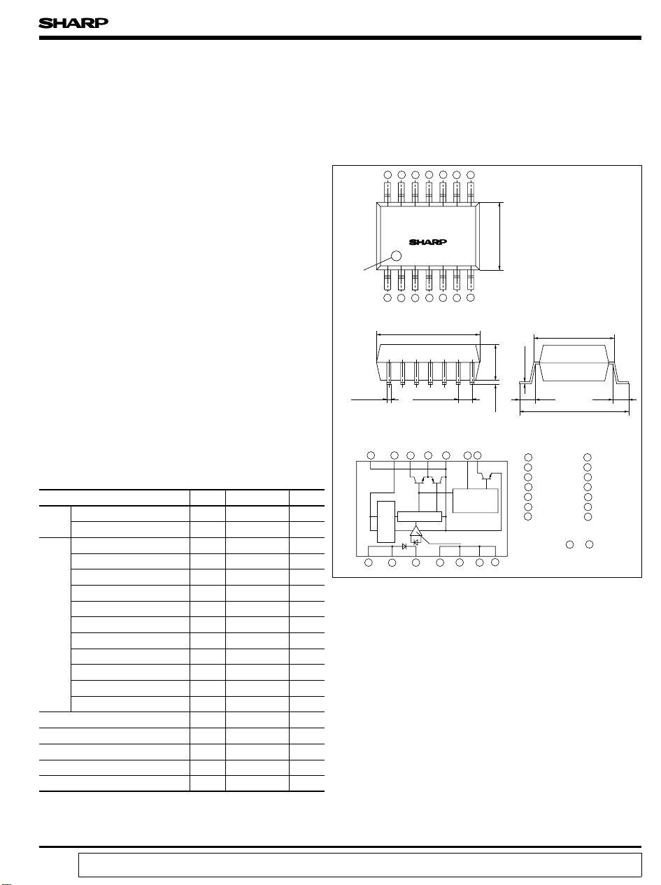
Outline Dimensions
■
PC928
Primary
side mark
1234567
9.22
14 - 0.6 12 - 1.27
1011121314
89
6.5
0.26
0.35 3.5
1.0 1.0
(Unit : mm)
7.62
10.0
Internal connection diagram
Absolute Maximum Ratings
■
*1
Forward current I
Input
Reverse voltage V
Supply voltage V
O1 output current
*4
peak output current
O
1
output current
O
2
*4
peak output current
O
2
O
Output
output voltage
1
*2
Power dissipation P
Overcurrent detecting voltage
Overcurrent detecting current
Error signal output voltage
Error signal output current
*3
Total power dissipation P
*5
Isolation voltage V
Operating temperature T
Storage temperature T
Soldering temperature T
*1, 2, 3 Decrease in the ambient temperature range of the Absolute Max. Rating : Shown in Figs. 1 and 2.
*4 Pulse width<=0.15µs, Duty ratio=0.01
*5 40 to 60% RH, AC for 1 minute, Ta=25˚C
(Ta=Topr unless otherwise specified)
Symbol UnitParameter
I
I
V
V
Rating
F
6 (Ta= 25˚C
R
CC
I
O1
O1P
I
O2
O2P
O1
O
V
C
I
C
FS
I
FS
tot
iso
- 25to + 80 ˚C
opr
- 55to + 125 ˚C
stg
260 (for 10 sec)
sol
25 mA
)
35 V
0.1 A
0.4 A
0.1 A
0.4 A
35 V
500 mW
V
CC
30 mA
V
CC
20 mA
550 mW
4 000
Vrms
V
V
V
˚C
* "OPIC" (Optical IC) is a trademark of the SHARP Corporation.
An OPIC consists of a light-detecting element and signal processing
circuit integrated onto a single chip.
89
1011121314
IGBT protector
Interface
Constant
voltage circuit
1234567
circuit
Amp.
1 Anode
2 Anode
3 Cathode
4NC
5NC
6NC
7NC
Terminals 4 to 7 :
Shortcircuit in element
Operation truth table is shown on the next page.
8FS
9C
10
GND
11
O
2
12
O
1
13
V
CC
14
GND
“ In the absence of confirmation by device specification sheets, SHARP takes no responsibility for any defects that occur in equipment using any of SHARP's devices, shown in catalogs,
data books, etc. Contact SHARP in order to obtain the latest version of the device specification sheets before using any SHARP's device.”
Page 2
PC928
Electro-optical Characteristics (1)
■
Parameter Symbol Conditions Unit
V
Forward voltage
Reverse current
Input
Terminal capacitance
Operating supply voltage
O
low level output voltage
1
O
high level output voltage
2
O2 low level output voltage
Output
leak current
O
1
High level supply current
Low level supply current
*7
"Low→High"
threshold input current
Isolation resistance R
"Low→High" propagation delay time
"High→Low" propagation delay time
Rise time t
Fall time t
Response time
Instantaneous common mode rejection
voltage "Output : High level"
Transfer characteristics
Instantaneous common mode rejection
voltage "Output : Low level"
*6 When measuring output and transfer characteristics, connect a bypass capacitor (0.01µ F or more) between Vcc and GND near the device.
*7 I represents forward current when O output goes from "Low" to "High".
FLH
*8 FS=OPEN, V =0V
C
2
V
V
V
V
V
I
I
I
I
t
t
CM
CM
I
C
O1L
O2H
O2L
O1L
CCH
CCL
FLH
ISO
PLH
PHL
F1
F2
R
t
CC
r
f
H
L
(Ta=Topr unless otherwise specified)
MIN. TYP. MAX.
Test circuit
Ta= 25˚C, IF= 20mA - 1.2 1.4 V Ta= 25˚C, IF= 0.2mA 0.6 0.9 - V Ta= 25˚C, VR=4V - - 10 µATa= 25˚C, V= 0, f = 1kHz - 30 250 pF Ta= - 10 to60˚C 15 - 30 V
- 15 - 24 V
V
= 12V, V
CC1
I
= 0.1A, IF= 10mA
O1
V
CC=VO1
I
= 10mA
F
VCC=VO1= 24V, IO2= 0.1A, IF= 0mA
Ta= 25˚C, VCC=VO1= 35V, IF= 0mA
Ta= 25˚C, VCC=VO1= 24V, IF= 10mA
VCC=VO1= 24V, IF= 10mA
Ta= 25˚C, VCC=VO1= 24V, IF= 0mA
VCC=VO1= 24V, IF= 0mA
Ta= 25˚C, VCC=VO1= 24V
VCC=VO1= 24V
= 25˚C, DC500V, 40to60%RH
T
a
Ta= 25˚C, VCC=VO1= 24V
RG=47Ω, CG= 3 000pF, IF= 10mA
Ta= 25˚C, VCC=VO1= 24V, IF= 10mA
VCM= 600V(peak), ∆ V
Ta= 25˚C, VCC=VO1= 24V, IF= 0mA
= 600V(peak), ∆ V
V
CM
= - 12V
CC2
= 24V, IO2= - 0.1A
= 2.0V
O2H
= 2.0V
O2L
- 0.2 0.4 V
*8
20 22 - V
*8
- 1.2 2.0
*8
- - 500
*8
-1017mA
*8
- - 19 mA
*8
-1118mA
*8
- - 20 mA
*8
1.0 4.0 7.0 mA
*8
0.6 - 10 mA
*8
5x10
10
1x10
11
--Ω
- 1.0 2.0 µs
- 1.0 2.0 µs
- 0.2 0.5 µs
*8
- 0.2 0.5 µs
- 1 500
*8
1 500
*8
13
--V/µs
--V/µs
14
V
µ A
-
(1)
(2)
(3)
(4)
(
)
6
(5)
(8)
(
)
7
■
Truth Table
Input
ON
OFF
O
Output FS OutputC Input/output
2
Low level High level High level
High level Low level Low level
Low level Low level High level
High level Low level High level
For protective operation
Page 3

PC928
Electro-optical Characteristics (2)
■
Parameter Symbol Conditions Unit
*9
*9
*9
*9 When measuring overcurrent, protective output and error signal output characteristics, connect a bypass capacitor (0.01µ F or more) between V and GND
*10 V represents C-terminal voltage when O output goes from "High" to "Low".
*10
Overcurrent detecting voltage
Overcurrent detecting voltage
detection
hysteresis width
Overcurrent
O2 "High→Low" delay time
at protection from overcurrent
O2 fall time at protection
from overcurrent
O2 output voltage at protection
Protective output
from overcurrent
Low level error
signal voltage
High level error
signal current
Error signal "High→Low"
delay time
Error signal output
Error signal output pulse width
CTH
V
V
t
PCOHL
t
PCOtf
V
CTH
CHIS
OE
Ta= 25˚C, IF= 10mA
V
C
= 24V, RG=47Ω
CC=VO1
= 3 000pF, FS= OPEN
G
Ta= 25˚C
V
C
C
= 24V, IF= 10mA
CC=VO1
= 3 000pF, RG=47Ω
G
= 1 000pF, RC=1kΩ
P
FS= OPEN
Ta= 25˚C, IF= 10mA, IFS= 10mA
V
FSL
VCC=VO1= 24V, RG=47Ω, CG= 3 000pF,
C = OPEN
T
= 25˚C, IF= 10mA, VFS= 24V,
I
FSH
a
V
= 24V, RG=47Ω, CG= 3 000pF,
CC=VO1
VC=0V
t
PCFHL
∆ t
2
Ta= 25˚C, RFS= 1.8kΩ
V
CC=VO1
CG= 3 000pF, RG=47Ω
FS
= 1 000pF, RC=1kΩ
C
P
= 24V, IF= 10mA
(Ta=Topr unless otherwise specified)
MIN. TYP. MAX.
VCC-VCC-VCC-
6.5 6.0 5.5
123V
-410
25-µs
--2V
- 0.2 0.4 V
- - 100 µ A(12
-15µs
20 35 - µ s
13
CC
Test circuit
V
µs
(13)
(10)
(11)
(14)
near the device.
14
(9)
)
Precautions for Operation
1. It is recommended that a capacitor of about 1000pF is added between C-terminal and GND in order to prevent
malfunction of C-terminal due to noise. In the case of capacitor added, rise of the detecting voltage is delayed.
Thus, use together a resistance of about 1kΩ set between Vcc and C-terminal.
The C-terminal rise time varies with the time constant of CR added. Make it clear before use.
2.
The light-detecting element used for this product is provided with a parasitic diode between each terminal and GND.
When a terminal happens to reach electric potential lower than GND potential even in a moment, malfunction
or rupture may result. Design the circuit so that each terminal will be kept at electric potential lower than the
GND potential at all times.
Page 4

Test Circuit Diagram
■
PC928
(1)(
12
↑ I
F
3
(
)(
3
12
↑ I
F
3
(
)(
5
12
↑
I
F
variable
3
SW
= 0mA
12
B
3
(
)
7
A
VCMwaveform
CM
, VO2waveform
H
SW at A, IF= 10mA
, VO2waveform
CM
L
SW at B, I
F
PC928
PC928
PC928
PC928
+-
V
CM
14
14
14
14
∆ V
13
12
11
10
9
8
13
12
11
10
9
8
13
12
11
10
9
8
13
12
11
10
9
8
L
O2
VO1L
V
V
L
V ↑
O2
V
V
O2
V
O2
V
∆ VO2H
I
O1
V
CC1
↑
V
CC2
V
CC
I
O2
V
CC
V
CC
(Peak)
V
CM
GND
H
V
O2
V
L
O2
GND
)
2
12
↑ I
F
3
)
4
)
6
(
)
8
tr= tf= 0.01 µ s
Pulse width : 5 µ s
V
IN
Duty ratio=50%
waveform
V
IN
V
waveform
OUT
12
↑
I
F
3
12
↑
I
F
3
12
3
PC928
PC928
PC928
PC928
t
pLH
13
12
11
10
14
9
8
13
12
11
10
14
9
8
13
12
11
10
14
9
8
13
12
11
10
14
9
8
t
pHL
t
r
↑
I
O2
V
CC
VO2H
V
A
I
O1L
V
OUT
50%
t
f
I
R
A
CC
G
90%
50%
10%
V
CC
V
CC
V
CC
C
G
(
)(
9
12
↑
I
F
3
PC928
13
12
11
V
10
14
9
8
V
R
OUT
V
CC
G
C
G
V
V
CTH
)
10
12
↑
I
F
3
PC928
13
12
11
V
10
14
9
8
V
R
CC
G
R
C
V
OE
C
P
L
G
V
C
Page 5

Test Circuit Diagram
■
PC928
(11)
↑ I
(13)
tr= tf= 0.01µ s
Pulse width : 25µ s
V
IN
Duty ratio=25%
(12)
13
12
F
3
PC928
12
11
10
14
9
8
V ↓V
FSLIFS
R
V
G
CC
C
G
↑ I
12
F
3
PC928
13
12
11
10
14
9
8
R
V
G
CC
C
G
V
I
FSH
A
FS
(14)
12
PC928 V
14
3
13
12
11
10
9
8
R
G
V
CC
C
V
OUT
C
P
G
R
C
tr= tf= 0.01µ s
Pulse width : 25µ s
V
IN
Duty ratio=25%
12
3
PC928
13
12
11
10
14
9
8
R
C
R
G
V
CC
C
G
R
FS
V
I
F
(Input current)
V
O2
(O2 output voltage)
C
(Detecting terminal)
FS
(Error signal output)
10%
t
pCFHL
t
pCOTF
90%
50%
10%
t
pCOHL
90%
50% 50%
OE
V
Error detecting threshold voltage (V )
∆ t
FS
CTH
Page 6

PC928
Fig. 1 Forward Current vs. Ambient
Temperature
60
50
40
F
30
20
Forward current I (mA)
10
0
0 25 50 75 80 100 125-25
Ambient temperature Ta(˚C)
Fig. 3 Forward Current vs. Forward Voltage
500
200
100
50
F
20
10
5
Forward current I (mA)
2
1
0 0.5 1.0 1.5 2.0 2.5 3.0 3.5
Ta= 75˚C
50˚C
25˚C
0˚C
- 20˚C
Forward voltage V (V)
F
Fig. 5 "L-H" Relative Threshold Input Current
vs. Ambient Temperature
1.3
FLH
1.2
1.1
I at Ta=25˚C = 1
FLH
1
VCC= 24V
Fig. 2 Power Dissipation vs. Ambient
Temperature
600
Total power dissipation
550
Output side power dissipation
500
400
300
200
100
Power dissipation Ptot, Po (mW)
0
0 25 50 75 80 100 125-25
Ambient temperature Ta(˚C)
Fig. 4 "L-H" Relative Threshold Input
Current vs. Supply Voltage
1.6
FLH
1.4
1.2
Value of V =24V assumes 1.
CC
1
0.8
Ta= 25˚C
Relative threshold input current I
0.6
15 18 21 24 27 30
Supply voltage V (V)
CC
Fig. 6 O1 Low Level Output Voltage vs.
O
Output Current
1
1
(V)
O1L
0.1
0.01
Ta = 25˚C
V
CC1
V
CC2
I
= 10mA
F
= 12V
= 12V
0.9
Relative threshold input current I
0.8
- 25 0 25 50 75 100
Ambient temperature Ta (˚C)
low level output voltage V
1
O
0.001
0.01 0.1 1
O1 output current I
(A)
O
1
Page 7

PC928
Fig. 7 O1 Low Level Output Voltage vs.
Ambient Temperature
0.25
0.20
O1L
0.15
0.10
0.05
low level output voltage V (V)
1
O
0.00
- 25 0 25 50 75 100
IO1= 0.1A
Ambient temperature Ta (˚C)
Fig. 9 O
High Level Output Voltage vs.
2
Supply Voltage
35
30
O2H
25
20
15
V
= 12V
CC1
V
= - 12V
CC2
IF= 10mA
Ta= 25˚C
= 10mA
I
F
I
= - 0.1A
O2
Fig. 8 O1 Leak Current vs. Ambient
Temperature
-6
10
-7
10
O1L
-8
10
leak current I (A)
1
O
-9
10
0 255075100-25
Ambient temperature Ta (˚C)
Fig. 10 O2 High Level Output Voltage vs.
Ambient Temperature
O2H
24
23
IO2=0A
22
- 0.1A
21
VCC= 24V
I
= 10mA
F
high level output voltage V (V)
10
2
O
5
15 18 21 24 27 30
Supply voltage V (V)
CC
Fig. 11 O2 Low Level Output Voltage vs.
Output Current
10
(V)
O2L
1
0.1
low level output voltage V
2
O
0.01
0.01 0.1 1
Output current IO2 (A)
V
= 24V
CC
Ta= 25˚C
20
high level output voltage V (V)
2
O
19
- 25 0 25 50 75 100
Ambient temperature Ta (˚C)
Fig. 12 O2 Low Level Output Voltage vs.
Ambient Temperature
1.3
(V)
1.2
O2L
1.1
1
0.9
low level output voltage V
2
O
0.8
- 25 0 25 50 75 100
I
O2
= 0.1A
Ambient temperature Ta (˚C)
V
CC
I
= 10mA
F
= 24V
Page 8

PC928
Fig. 13 High Level Supply Current vs.
Supply Voltage
14
IF= 10mA
Ta= - 25˚C Ta= - 25˚C
12
CCH
10
8
25˚C
80˚C
6
High level supply current I (mA)
4
15 18 21 24 27 30
Supply voltage V (V)
CC
Fig. 15 Propagation Delay Time vs.
Forward Current
3.5
3
(µ s)
2.5
PLH
, t
PHL
t
PLH
2
1.5
1
0.5
t
Propagation delay time t
PHL
0
0 5 10 15 20 25
Forward current IF (mA) Ambient temperature Ta (˚C)
Ta= 25˚C
= 24V
V
CC
R
=47Ω
G
CG= 3 000pF
Fig. 14 Low Level Supply Current vs.
Supply Voltage
16
IF= 0mA
14
CCL
12
10
25˚C
80˚C
8
Low level supply current I (mA)
6
15 18 21 24 27 30
Supply voltage V (V)
CC
Fig. 16 Propagation Delay Time vs.
Ambient Temperature
2.5
2
(µ s)
PLH
, t
PHL
1.5
t
1
0.5
Propagation delay time t
0
- 25 0 25 50 75 100
PLH
t
PHL
= 24V
V
CC
RG=47Ω
CG= 3 000pF
I
= 10mA
F
Fig. 17 Overcurrent Detecting Voltage vs.
Ambient Temperature
30
(V)
25
CTH
20
15
10
5
Overcurrent detecting voltage V
0
- 25 0 25 50 75 100
Ambient temperature Ta (˚C)
VCC= 24V
=47Ω
R
G
CG= 3 000pF
I
= 10mA
F
Fig. 18
O2 Output Fall Time at Protection from Overcurrent/O
"H-L"
2
Delay Time at Protection from Overcurrent vs. Ambient temperature
10
VCC= 24V
I
= 10mA
F
R
=47Ω
G
C
= 3 000pF
G
8
R
=1kΩ
C
C
= 1 000pF
P
6
4
2
output fall time at protection from overcurrent tpcotf/
"H-L" delay time at protection from overcurrent tpcoHL ( µ s)
2
2
0
O
O
- 25 0 25 50 75 100
Ambient temperature Ta (˚C)
t
t
pcoHL
pcotf
Page 9

PC928
Fig. 19 Error Signal "H-L" Delay Time vs.
Ambient Temperature
(µ s)
pcfHL
1.5
1.2
0.9
VCC= 24V
I
= 10mA
F
R
= 1.8kΩ
FS
R
=47Ω
G
CG= 3 000pF
R
=1kΩ
C
C
= 1 000pF
P
0.6
0.3
Error signal "H-L" delay time t
0
- 25 0 25 50 75 100
Ambient temperature Ta (˚C)
Fig. 21 Low Level Error Signal Voltage vs.
Ambient Temperature
0.5
= 24V
V
CC
I
= 10mA
F
IFS= 10mA
(V)
0.4
R
=47Ω
G
FSL
C
= 3 000pF
G
C= OPEN
0.3
0.2
0.1
Low level error signal voltage V
0
- 25 0 25 50 75 100
Ambient temperature Ta (˚C)
Fig. 20 O2 Output Voltage at Protection from
Overcurrent vs. Ambient Temperature
2
(V)
OE
1.6
1.2
V
CC
I
= 10mA
F
=47Ω
R
G
C
= 3 000pF
G
R
=1kΩ
C
C
= 1 000pF
P
= 24V
0.8
0.4
output voltage at protection from overcurrent V
2
0
O
- 25 0 25 50 75 100
Ambient temperature Ta (˚C)
Fig. 22 High Level Error Signal Current vs.
Ambient Temperature
-6
10
VCC= 24V
I
= 10mA
F
VFS= 24V
(A)
R
=47Ω
G
FSH
C
= 3 000pF
G
V
=0V
C
-7
10
-8
10
High level error signal current I
-9
10
- 25 0 25 50 75 100
Ambient temperature Ta (˚C)
Fig. 23 Error Signal Output Pulse Width vs.
Ambient Temperature
50
VCC= 24V
I
= 10mA
F
R
= 1.8kΩ
FS
(µ s)
40
FS
R
=47Ω
G
= 3 000pF
C
G
=1kΩ
R
C
= 1 000pF
C
P
30
20
10
Error signal output pulse width∆ t
0
- 25 0 25 50 75 100
Ambient temperature Ta (˚C)
Page 10

PC928
Fig. 24 Overcurrent Detecting Voltage
vs. Supply Voltage
25
Ta= 25˚C
I
= 10mA
F
V
= 24V
(V)
CTH
CC
20
R
G
CG= 3 000pF
R
C
FS= OPEN
15
C
P
10
=47Ω
=1kΩ
= 1 000pF
Added resistance=0 Ω
0.5kΩ
1kΩ
5
Overcurrent detecting voltage V
0
15 18 21 24 27 30
1.5kΩ
Supply voltage Vcc (V)
Application Circuit (IGBT Drive for Inverter)
Anode
Anode
Cathode
TTL, microcomputer, etc.
Feedback to primary side
V
CC
O
1
O
2
PC928
C
FS
GND
+
R
G
R
C
+
Overcurrent Detecting Voltage Supply Voltage Characteristics Test Circuit
Anode
I
F
Cathode
V
= 12V
CC1
IGBT
U
CP
V
= 12V
CC2
V
CC
O
O
PC928
C
FS
GND
V
Added resistance
C
G
CC
V
C
V
(+)
W
1
R
2
G
R
V
C
V
O2
C
P
V
Power supply
(-)
■
Operations of Shortcircuit Protector Circuit
Anode
Anode
TTL, microcomputer, etc.
1. Detection of increase in V
Cathode
CE(sat)
Light emitting diode
1
2
Constant voltage circuit
3
Photodiode
of IGBT due to overcurrent by means of C-terminal ( terminal)
PC928
Amp.
Interface
IGBT protector circuit
GND
14
V
CC
13
O
1
12
O
2
11
R
G
C
9
FS
8
GND
10
Feedback to primary side
9
V
CC
IGBT
R
C
C
P
V
EE
2. Reduction of the IGBT gate voltage, and suppression of the collector current
3. Simultaneous issue of signals to indicate the shortcircuit condition (FS signal) from FS terminal to the microcomputer
4. Judgement and processing by the microcomputer
In the case of instantaneous shortcircuit, run continues.
At fault, input to the photocoupler is cut off, and IGBT is turned OFF.
 Loading...