

Page 1
PC912X
PC912X
Ultra-high Speed Response
OPIC Photocoupler
1. Ultra-high speed response
(t
PHL
, t
PLH
: TYP. 40ns
)
2. High instantaneous common mode rejection
voltage (CM
: MIN. 3kV/µs
H
)
3. Capable of high speed digital transmission
(Transmission speed : MAX. 20Mb/s
(NRZ signal
)
)
■ Applications
1. Personal computers
2. Electrical music instruments
■ Absolute Maximum Ratings
Parameter Symbol Rating Unit
*1
Forward current I
Input
Output
*1 Ta= 0 to 70˚C
*2 It shall not exceed 500mV or more over supply voltage (V
*3 Applied to output terminal (V
*4 AC for 1 minute, 40 to 60%RH
*5 For 10 seconds
Reverse voltage
*1
Power dissipation
Supply voltage
*2
Enable voltage
High level output current
Low level output current
*1, 3
Collector power
dissipation
*4
Isolation voltage V
Operating temperature T
Storage temperature T
*5
Soldering temperature T
)
O
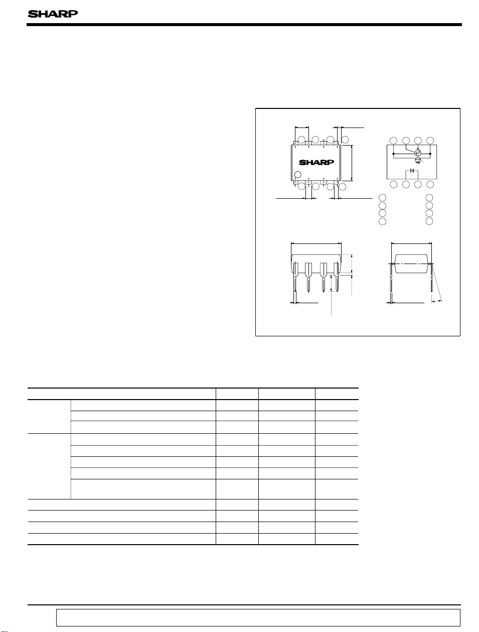
■ Outline Dimensions■ Features
± 0.5
3.7
mW
kV
± 0.2
0.8
5678
± 0.5
6.5
± 0.3
0.85
± 0.5
3.5
TYP.
0.5
)
V
V
V
rms
˚C
± 0.25
2.54
PC912
12 34
± 0.3
1.2
± 0.5
9.22
± 0.1
0.5
* “OPIC ” (Optical IC) is a trademark of the SHARP Corporation.
An OPIC consists of a light-detecting element and signal processing circuit integrated onto a single chip.
(
Ta= 25˚C
F
V
R
P
V
CC
V
E
I
OH
I
OL
P
O
iso
opr
stg
sol
)
.
CC
20 mA
5
40
7
7
-8 mA
25 mA
40 mW
2.5
0 to + 70 ˚C
- 55 to + 125
260 ˚C
(
Unit : mm
Internal connection
diagram
1234
1 NC
2 Anode
3 Cathode
4 NC
± 0.3
7.62
± 0.1
0.26
θ : 0 to 13 ˚
Amp.
5678
5 GND
6 V
O
7 V
E
8 V
CC
θ
)
“ In the absence of confirmation by device specification sheets, SHARP takes no responsibility for any defects that occur in equipment using any of SHARP's devices, shown in catalogs,
data books, etc. Contact SHARP in order to obtain the latest version of the device specification sheets before using any SHARP's device. ”
Page 2
PC912X
■ Electro-optical Characteristics
Parameter Symbol Conditions MIN. TYP. MAX. Unit
Forward voltage V
Input
Output
Transfer
characteristics
*6 Refer to Fig. 1 *7 Refer to Fig. 2 *8 Refer to Fig. 3
All typical values are at Ta= 25˚C, V
Reverse current I
Terminal capacitance C
High level output voltage V
Low level output voltage V
High level enable voltage V
Low level enable voltage V
High level enable current I
Low level enable current I
High level supply current I
Low level supply current I
High impedance supply
current
Output leak current I
High impedance output
current
Output short-circuit current I
“High→Low” threshold input current
“Low→High” threshold input current
Hysteresis
Isolation resistance
Floating capacitance C
“ High→Low” propagation
delay time
“ Low→High” propagation
delay time
Response
time
Pulse width distortion
t
PHL-tPLH
Rise/fall time t
“ High→Low” enable
propagation delay time
“ Low→High” enable
propagation delay time
Instantaneous common
mode rejection voltage
CMR
(
High level output
Instantaneous common
)
mode rejection voltage
(
Low level output
CC
)
= 5V.
R
OH
OL
EH
EH
EL
CCH
CCL
I
CCZ
OH
I
OZH
OS
I
FHL
I
FLH
I
FLH/IFHL
R
ISO
t
PHL
t
PLH
∆
T
, t
r
t
EHL
t
ELH
CM
CM
(
Unless specified : Ta= 0 to 70˚C
Ta= 25˚C, IF= 10mA - 1.6 1.9 V
F
Ta= 25˚C, VR=5V - - 10 µA
Ta= 25˚C, VF=0V
t
f= 1MHz
VCC= 4.5V, IOH= - 2mA
IF= 0.25mA, VE= 2.0V
VCC= 4.5V, VE= 2.0V
= 5mA, IOL= 13mA
I
F
- 60 120 pF
2.4 - - V
- 0.3 0.6 V
VCC= 5.5V 2.0 - - V
VCC= 5.5V - - 0.8 V
EL
VCC= 5.5V, VE= 5.5V - - 100 µ A
VCC= 5.5V, VE= 0.5V - - 0.2 - 0.4 mA
VCC= 5.5V, IF= 0mA
= 2.0V
V
E
VCC= 5.5V, IF= 10mA
= 2.0V
V
E
-1323mA
-1525mA
VCC= 5.5V, VE= 0V - 16 26 mA
VCC= 5.5V, VE= 2.0V
= 5.5V, IF= 0.25mA
V
O
- - 100 µ A
VCC= 5.5V, VE= 0.4V - - 100 µ A
VCC= 5.5V, VO=0V
= 0mA
I
F
-10 - -50 mA
10ms or less
VCC=5V
V
E
Ta= 25˚C, DC= 500V
40 to 60%RH
Ta= 25˚C, V= 0V
f
f=1MHz
= 2.0V
- 2.5 5 mA
0.5 1.9 - mA
0.55 - 0.95 -
5x101010
11
- 0.6 5 pF
-4055
Ta= 25˚C
V
=5V
CC
= 15pF
C
L
= 7.5mA
I
F
w
*6
f
Ta= 25˚C, V
CC
=5V
RL= 350Ω, CL= 15pF
= 7.5mA, VEH=3V
I
F
= 0V, *7
V
EL
Ta= 25˚C, V
VCM= 50V, IF= 0mA -
H
(
Min)= 2V, *8
V
O
Ta= 25˚C, V
VCM= 50V, IF= 5mA -
L
(
V
Max)= 0.8V, *8
O
CC
CC
=5V
=5V
-4055
--15
-1530
-4070
-4070
3 000 10 000
- 3 000 10 000
)
- Ω
ns
ns
ns
ns
ns
ns
V/ µ s
V/ µ s
Page 3

■ Recommended Operating Conditions
Parameter Symbol MIN. MAX. Unit
Low level input current I
High level input current I
High level enable voltage V
Low level enable voltage V
Supply voltage V
Fan out (TTL load
)
FL
FH
EH
EL
CC
N-8-
0 250 µA
715mA
2.0 V
CC
0 0.8 V
4.5 5.5 V
Operating temperature Topr 0 70 ˚C
1. When the enable input is not used, please connect to Vcc.
2. It is necessary to connect a by-pass ceramic capacitor
(0.01 to 0.1µF) between Vcc and GND at the position within
1cm from pin.
■ Block Diagram
Anode 2
Cathode 3
8 V
CC
7 V
E
(Enable
6 V
O
5 GND
)
Buffer
circuit
(
*
Positive logic
1.6kΩ
(TYP.
1kΩ
(TYP.
)
)
)
PC912X
V
V
130Ω
(TYP.
CC
)
V
E
*
Positive logic:
VEBuffer output
V
O
LL
HH
GND
■ Truth Table
Input Enable Output
HHL
LHH
HLZ
LLZ
Fig. 1 Test Circuit for t
I
F
47Ω
PHL
L : Logic (0
H : Logic (1
)
)
Z : High impedance
, t
, tr and t
PLH
f
0.1µ F
C
L
* CL includes the probe and wiring capacitance.
90%
10%
7.5mA
3.75mA
0mA
5V
1.5V
V
OL
5V
I
F
t
V
O
PHL
V
O
t
f
t
PLH
t
r
Page 4

PC912X
Fig. 2 Test Circuit for t
Pulse input V
and t
EHL
E
ELH
IF=7.5mA
*C
L includes the probe and wiring capacitance
Fig. 3 Test Circuit for CMH and CM
I
F
V
CM
3V
0.1µF
350Ω
C
L
5V
V
E
t
V
O
EHL
V
O
t
ELH
1.5V
0V
5V
1.5V
V
OL
L
50V
0.1µ F
C
L
(
I
F
(
I
F
V
O
= 0mA
V
O
= 5mA
V
CM
)
)
0V
5V
(
)
V
MIN.
O
(
)
V
MAX.
O
V
OL
Fig. 4 Forward Current vs.
Forward Voltage
100
= 70˚C
T
a
)
10
mA
(
F
1
0.1
Forward current I
0.01
1.2 2.2 0
Forward voltage VF (V
T
T
a
= 25˚C
a
T
a
= 50˚C
= 0˚C
2.01.81.61.4
)
Fig. 5 Low Level Output Voltage vs.
Low Level Output Current
10
VCC=5V
I
= 5mA
F
Ta= 70˚C
= 25˚C
T
a
Ta= 0˚C
)
0.5
)
0.4
V
(
OL
0.3
= 0˚C
T
a
0.2
0.1
Low level output voltage V
Ta= 25˚C
T
= 70˚C
a
0
Low level output current IOL (mA
20
Page 5

Fig. 6 High Level Output Voltage vs. Fig. 7 Propagation Delay Time vs.
High Level Output Current
T
= 25˚C
a
OH
VCC=5V
I
= 0.25mA
F
)
4.5
)
V
4.0
(
OH
T
= 70˚C
a
3.5
3.0
= 0˚C
T
a
2.5
High level output voltage V
2.0
0-10
-2 -4 -6 -8
High level output current I(mA
Ambient Temperature
100
)
ns
75
(
PLH
, t
PHL
50
25
Propagation delay time t
0
02550 75
t
PHL
t
PLH
Ambient temperature T
VCC=5V
= 7.5mA
I
F
(˚C)
a
Fig. 8 Propagation Delay Time vs.
Forward Current
100
)
ns
75
(
PLH
, t
PHL
50
25
t
PLH
t
PHL
VCC=5V
= 25˚C
T
a
PC912X
100
Propagation delay time t
0
0255075
Forward current I
Please refer to the chapter “Precautions for Use ”
●
F
(mA)
100
 Loading...