

Page 1
Ultra-high Speed Response and
PC911
❈ Lead forming type (I type) and taping reel type (P type) are also available. (PC911I/PC911P)
High CMR OPIC Photocoupler
PC911
■ Features
1. Ultra-high speed response
(t
PHL
, t
PLH
: TYP. 50ns
)
2. High instantaneous common mode rejec tion voltage (CM
: TYP. 10kV/µs
H
)
3. High isolation voltage
(V
: 4 000V
iso rms
)
4. Recognized by UL, file No. E64380
■ Applications
1. High speed interfaces for computer periph erals and microcomputer systems
2. High speed line receivers
3. Interfaces with various data transmission
equipment
■ Absolute Maximum Ratings
Parameter Symbol Rating Unit
*1
Forward current
Input
Output
*1 Ta= 0 to 70˚C
*2 Shall not exceed 500mV from supply voltage (Vcc).
*3 Applicable to output terminal(V
*4 AC for 1 minute, 40 to 60%RH
*5 For 10 seconds at the position of 2mm or more from root of lead pins.
Reverse voltage V
*1
Power dissipation
Supply voltage V
*2
Enable voltage
High level output current V
Low level output current I
*1
Power dissipation
*3
*4
Isolation voltage
Operating temperature T
Storage temperature T
*5
Soldering temperature
)
o
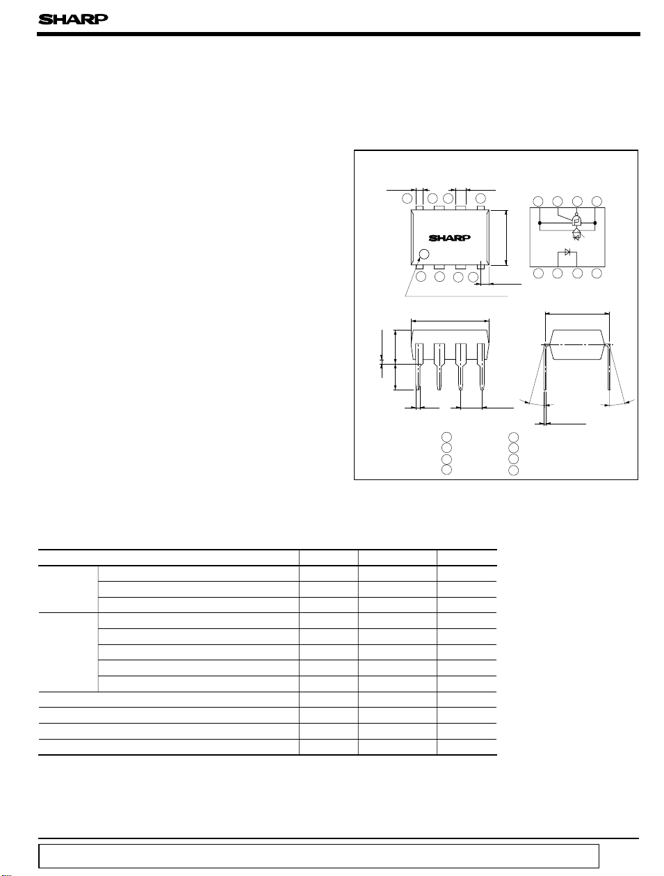
■ Outline Dimensions
± 0.3
0.85
PC911
1234
Primary side mark (Sunken place
9.22
± 0.5
TYP.
0.5
3.5
± 0.5
3.7
0.5
* “OPIC ” (Optical IC) is a trademark of the SHARP Corporation.
An OPIC consists of a light-detecting element and signal processing circuit integrated onto a single chip.
(
Ta= 25˚C
I
F
R
20 mA
5V
P40mW
CC
V
E
OH
OL
P
V
iso
opr
stg
T
sol
7V
7V
-8 mA
25 mA
40 mW
4 000
0 to + 70 ˚C
- 55 to + 125 ˚C
260
1.2
± 0.5
± 0.1
1 NC
2 Anode
3 Cathode
4 NC
V
rms
˚C
± 0.3
5678
2.54
)
0.8
± 0.5
6.5
± 0.2
)
±0.25
5 GND
6 V
7 V
8 V
(
Unit : mm
Internal connection
diagram
65
78
Amp
1234
± 0.3
7.62
θ
= 0 ˚ to 13 ˚
θ
± 0.1
0.26
O
E
CC
)
θ
“ In the absence of confirmation by device specification sheets, SHARP takes no responsibility for any defects that occur in equipment using any of SHARP's devices, shown in catalogs,
data books, etc. Contact SHARP in order to obtain the latest version of the device specification sheets before using any SHARP's device. ”
Page 2
PC911
■ Electro-optical Characteristics
Parameter MIN. TYP. MAX. Unit
Forward voltage - 1.6 1.9 V
Input
Output
Transfer
charac-
teristics
*6 TW=t
∆
Reverse current - - 10 µA
Terminal capacitance - 60 120 pF
High level output voltage 2.4 - - V
Low level output voltage - 0.3 0.6 V
High level enable voltage 2.0 - - V
Low level enable voltage - - 0.8 V
High level enable current - - 100 µA
Low level enable current - - 0.2 - 0.4 mA
High level supply current - 13 23 mA
Low level supply current - 15 25 mA
High impedance supply current - 16 26 mA
Output leak current - - 100 µA
High impedance output current - - 100 µA
Output short-circuit current - 10 - - 50 mA
“High→Low ” threshold
input current
“Low→High ” threshold
input current
Hysteresis 0.55 - 0.95 Isolation resistance 5 x 10
Floating capacitance - 0.6 5 pF
“ High→Low ”
propagation delay time
“ Low→High ”
propagation delay time
*6
Pulse width distortion - - 35
Rise time, Fall time - 15 30
“ High→Low ” enable
propagation delay time
Rsponse characteristics
“ Low→High ” enable
propagation delay time
Instantaneous common mode
rejection voltage “ output :
High level”
Instantaneous common mode
CMR
rejection voltage “ output :
Low level”
PHL-tPLH
Symbol Conditions
Ta= 25˚C, IF= 10mA
V
F
Ta= 25˚C, VR=5V
I
R
Ta= 25˚C, V = 0, f= 1MHz
C
t
VCC= 4.5V, IOH= - 2mA, IF= 0.25mA,
V
OH
V
= 0.2V
E
V
V
V
I
I
I
CCHVCC
I
CCLVCC
I
CCZVCC
I
OHVCC
I
OZHVCC
I
OSVCC
I
FHLVCC
I
FLHVCC
I
FLH/IFHLVCC
R
= 4.5V, VE= 2.0V, IF= 5mA, IOL= 13mA
OLVCC
EHVCC
ELVCC
EH
EL
= 5.5V
= 5.5V
VCC= 5.5V, VE= 5.5V
VCC= 5.5V, VE= 0.5V
= 5.5V, IF= 0, VE= 2.0V
= 5.5V, IF= 10mA, VE= 2.0V
= 5.5V, VE=0
= 5.5V, VE= 2.0V, VO= 5.5V, IF= 0.25mA
= 5.5V, V
= 5.5V, VO= 0, IF= 0, within 10ms.
= 5V, VE= 2.0V
= 5V, VE= 2.0V
= 5V, VE= 2.0V
Ta= 25˚C, DC500V, 40 to 60% RH
ISO
= 0.4V
E
CfTa= 25˚C, V = 0, f= 1MHz
t
PHL
Ta= 25˚C, VCC=5V
t
PLH
C
= 15pF
L
I
= 7.5mA, Fig. 1
∆
t
CM
CM
F
T
W
, t
r
f
Ta= 25˚C, VCC=5V
t
EHL
R
= 350 Ω, CL= 15pF
L
I
= 7.5mA, VEH=3V
F
t
ELH
V
= 0, Fig. 2
EL
Ta= 25˚C, VCC= 5V, VCM= 50V
H
I
= 0mA, V
F
Ta= 25˚C, VCC= 5V, VCM= 50V
L
IF= 5mA, V
O(MIN.
O(MAX.
)
= 2V, Fig. 3
)
= 0.8V, Fig. 3
(
Ta= 0 to 70˚C unless specified
- 2.5 5 mA
0.5 1.9 - mA
10
11
10
- Ω
-5075
-5075
-4070
-4070
3 000 10 000
- 3 000
All typical values : at Ta= 25˚C, Vcc=5V
- 10 000
-V/µs
-V/µs
)
ns
ns
ns
ns
ns
ns
Page 3

■ Recommended Operating Conditions
Parameter Symbol MIN. MAX. Unit
Low level input current I
High level input current I
High level enable voltage V
Low level enable voltage V
Supply voltage V
Fanout (TTL load
)
Operating temperature T
FL
FH
EH
EL
CC
N-8-
opr
1. When the enable input is not used, please connect to VCC.
2. In order to stabilize power supply line, connect a by-pass ceramic
capacitor (0.01 to 0.1µF) between V
1cm from pin.
and GND at the position within
CC
0 250 µA
715mA
2.0 V
0 0.8 V
4.5 5.5 V
070˚C
PC911
CC
V
Block Diagram
Anode
Cathode
Fig. 1 Test Circuit for t
Pulse input
Fig. 2 Test Circuit for t
47Ω
I
F
V
CC
V
E
V
O
GND
, t
PHL
CL includes the probe
and wiring capacitance.
, tr and t
PLH
and t
EHL
Pulse input V
ELH
E
(
Enable
f
)
0.1µ F
C
L
Truth table
Input Enable Output
HHL
LHH
HLZ
LLZ
L : Logic (0
H : Logic (1
Z : High impedance
5V
V
O
)
)
I
F
t
PHL
V
O
t
f
t
PLH
90%
10%
t
r
7.5mA
3.75mA
0mA
5V
1.5V
V
OL
IF=7.5mA
C
includes the probe
L
and wiring capacitance.
0.1
µF
5V
RL= 350Ω
V
O
C
L
3V
t
ELH
1.5V
0V
5V
1.5V
V
OL
V
E
t
EHL
V
O
Page 4

PC911
Fig. 3 Test Circuit for CMH and CM
I
F
V
CM
L
0.1µ F
Fig. 4 Forward Current vs. Forward Voltage
100
)
10
mA
(
F
1
Forward current I
0.1
Ta= 0˚C
25˚C
50˚C
70˚C
5V
V
CM
V
O
C
L
(
I
(
I
=5mA
F
V
O
)
=0
F
V
O
)
50V
0V
V
V
V
V
OH
O
O
OL
(
MIN.
(
MAX.
)
)
Fig. 5 Low Level Output Voltage vs.
Low Level Output Current
0.5
)
V
0.4
(
OL
0.3
0.2
0.1
Low level output voltage V
V
I
F
T
CC
= 5mA
= 25˚C
a
=5V
0.01
1.0
1.2 1.4 1.6 1.8 2.0 2.2
Forward voltage V
(V)
F
Fig. 6 High Level Output Voltage vs.
High Level Output Current
4.5
)
V
4.0
(
OH
3.5
3.0
2.5
High level output voltage V
2.0
0
-2 -4 -6 -8 -10
High level output current I
V
I
F
T
OH
=5V
CC
= 0.25mA
= 25˚C
a
(mA)
0
02010 15
5
Low level output current I
OL
Fig. 7 Propagation Delay Time vs.
Ambient Temperature
100
)
ns
(
75
PLH
, t
PHL
50
25
Propagation delay time t
0
0255075
Ambient temperature T
t
t
(˚C)
a
(mA)
VCC=5V
= 7.5mA
I
F
PLH
PHL
Page 5

Fig. 8 Propagation Delay Time vs.
Forward Current
100
V
=5V
PLH
PHL
CC
= 25˚C
T
a
)
)
ns
(
75
PLH
, t
PHL
50
25
Propagation delay time t
0
Please refer to the chapter “Precautions for Use ”
●
5 1015200
Forward current IF (mA
t
t
PC911
 Loading...