

Page 1
PC910X
PC910X
Ultra-high Speed Response
OPIC Photocoupler
■ Features
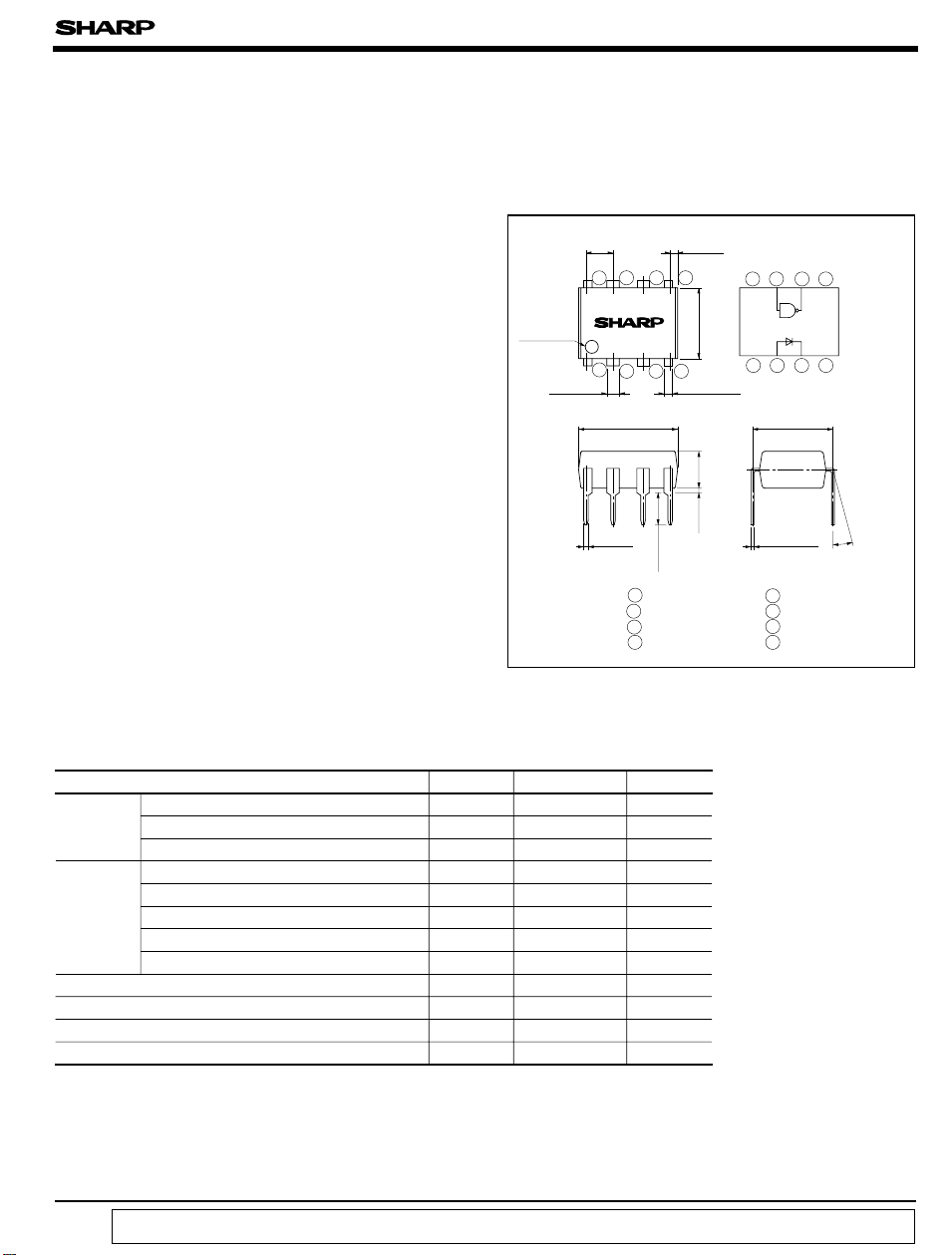
■ Outline Dimensions
1. Ultra-high speed response
(t
PHL
, t
: TYP. 50ns at RL= 350Ω
PLH
)
2. Isolation voltage between input and output
(Viso : 2 500V
3. Low input current drive (I
)
rms
: MAX. 5mA
FHL
)
4. Instantaneous common mode rejection
voltage (CMH: TYP. 500V/µs
)
5. TTL and LSTTL compatible output
6. Recognized by UL, file No. E64380
■ Applications
1. High speed interfaces for computer periph erals and microcomputer systems
2. High speed line receivers
3. Noise-cut
4. Interfaces with various data transmission
equipment
* “OPIC ” (Optical IC) is a trademark of the SHARP Corporation.
An OPIC consists of a light-detecting element and signal processing circuit integrated onto a single chip.
■ Absolute Maximum Ratings
Parameter Symbol Rating Unit
*1
Forward current
Input
Reverse voltage V
Power dissipation P 40 mW
*2
Supply voltage
*3
Enable voltage
Output
High level output voltage V
Low level output current I
Collector power dissipation P
*4
Isolation voltage
Operating temperature
Storage temperature
*5
Soldering temperature
*1 Ta= 0 to 70˚C
*2 For 1 minute max.
*3 Shall not exceed 500mV from supply voltage (V
*4 AC for 1minute, 40 to 60%RH. Apply the specified voltage between the whole o
input side and the whole of the electrode pins on the output side.
*5 For 10 seconds at the position of 2mm or more from lead pins.
)
.
CC
I
F
R
V
CC
V
E
OH
OL
C
V
iso
T
opr
T
stg
T
sol
± 0.25
2.54
Primary
side
mark
(
Sunken
place
)
12 34
± 0.3
1.2
0.5
PC910
± 0.5
9.22
± 0.1
± 0.5
3.7
1 NC
2 Anode
3 Cathode
4 NC
(
Ta= 25˚C
20 mA
5V
7V
5.5 V
7V
50 mA
85 mW
2 500
V
0 to + 70 ˚C
- 55 to + 125 ˚C
260 ˚C
f the electrode pins on the
0.8
5678
0.85
± 0.2
± 0.5
6.5
± 0.3
± 0.5
3.5
TYP.
0.5
(
Unit : mm
Internal connection
diagram
5678
1234
± 0.3
7.62
± 0.1
0.26
θ : 0 to 13 ˚
5 GND
6 V
O
7 V
E
8 V
CC
θ
)
)
rms
“ In the absence of confirmation by device specification sheets, SHARP takes no responsibility for any defects that occur in equipment using any of SHARP's devices, shown in catalogs,
data books, etc. Contact SHARP in order to obtain the latest version of the device specification sheets before using any SHARP's device.”
Page 2
PC910X
■ Electro-optical Characteristics
Parameter Symbol Conditions MIN. TYP. MAX. Unit
Forward voltage V
Input
Output
Transfer
charac-
teristics
Reverse current I
Terminal capacitance C
High level output current I
Low level output voltage V
High level enable current I
Low level enable current I
High level supply current I
Low level supply current I
“High→Low ” threshold
input current
Isolation resistance
Floating capacitance
“ High→Low” propagation
delay time
“ Low→High” propagation
delay time
Rise time, Fall time
“ High→Low” enable
Response time
propagation delay time
“ Low→High” enable
propagation delay time
Instantaneous common
mode rejection voltage
“ Output : High level ”
Instantaneous common
CMR
mode rejection voltage
“ Output : Low level ”
(
Unless otherwise specified, Ta = 0 to 70˚C
Ta= 25˚C, IF= 10mA
F
Ta= 25˚C, VR=5V - - 10 µA
R
Ta= 25˚C, V= 0, f = 1MH
t
VCC=VO= 5.5V, VE= 2.0V, IF= 250 µ A
OH
VCC= 5.5V, VE= 2.0V, IF= 5mA, IOL= 13mA
OL
EHVCC
EL
CCH
CCLVCC
I
FHL
R
iso
C
f
t
PHL
t
PLH
tr, t
t
EHL
t
ELH
CM
CM
= 5.5V, VE= 2.0V - - 0.8 - 1.8 mA
V
= 5.5V, VE= 0.5V
CC
= 5.5V, IF= 0, VE= 0.5V
V
CC
= 5.5V, IF= 10mA, VE= 0.5V
VCC= 5V, VE= 2.0V
= 0.8V, RL= 350Ω
V
O
Ta = 25˚C, DC500V, 40 to 60% RH
Ta= 25˚C, V= 0, f = 1MH
Ta= 25˚C, VCC=5V
= 350Ω, CL=15PF
R
L
I
= 7.5mA
F
f
Ta= 25˚C, VCC=5V
= 350Ω, CL= 15pF
R
L
= 7.5mA, VEH=3V
I
F
= 0.5V
V
EL
Ta = 25˚C, VCC= 5V, VCM= 10V
H
RL= 350Ω, IF= 0, V
Ta = 25˚C, VCC= 5V, VCM= 10V
L
RL= 350Ω, IF= 5mA V
O(MIN
)
=2V
(
peak
O(MAX
(
)
)
peak
)
= 0.8V
Z
Z
- 1.6 1.9 V
- 60 150
- 2 250 µ A
- 0.4 0.6 V
- - 1.2 - 2.0 mA
- 7 15 mA
-1318mA
- 2.5 5 mA
10
5x10
10
10
- 0.6 5
Fig. 1
- 50 120 ns
- 50 120 ns
-3060ns
Fig. 2
-1550ns
- 65 100 ns
Fig. 3
100 500 - V/ µ s
Fig. 3
- 100 - 500 - V/ µ s
All typical values : at Ta= 25˚C, VCC=5V
- Ω
P
pF
)
F
■ Recommended Operating Conditions
Parameter Symbol MIN. MAX. Unit
Low level input current I
High level input current I
High level enable voltage V
Low level enable voltage V
Supply voltage V
Fanout (TTL load
)
Operating temperature T
FL
FH
EH
EL
CC
N-8-
opr
1. When the enable input is in high level state, extemal pull-up resistor is
unnecessary.
2. Connect a by-pass ceramic capacitor (0.01 to 0.1µF) between
and GND at the position within 1cm from pin.
V
CC
0 250 µA
715mA
2.0 V
0 0.8 V
4.5 5.5 V
070˚C
CC
V
Page 3

Circuit Block Diagram
Anode
Cathode
V
CC
V
E
(
Enable
V
O
GND
PC910X
Truth Table
Input Enable Output
)
HHL
LHH
HLH
LLH
L : Logic (0
H : Logic (1
)
)
Fig. 1 Test Circuit for t
PHL
, t
, tr and t
PLH
1
I
Pulse input
F
2
3
47Ω
Fig. 2 Test Circuit for t
V
E
45
and t
EHL
ELH
Pulse input
1
IF= 7.5mA
2
3
Fig. 3 Test Circuit for CMH and CM
f
8
7
6
0.1µF0.1µF
*CL includes the probe
and wiring capacitance.
8
7
6
54
L
350Ω
C
L
350Ω
C
L
7.5mA
I
5V
V
O
F
t
PHL
90%
V
O
10%
t
f
3.75mA
t
0mA
PLH
5V
1.5V
V
OL
t
r
3V
V
5V
V
O
E
t
EHL
V
O
1.5V
t
0.5V
ELH
5V
1.5V
V
OL
10V
GL SW
B
350Ω
C
L
5V
V
V
(
I
F
V
(
I
F
O
= 0mA
O
= 5mA
CM
)
)
5V
V
V
V
0V
O(MIN.
O(MAX.
OL
)
)
When the switch for
infrared light emitting
diode sets to A
When the switch for
infrared light emitting
diode sets to B
I
1
F
2
A
3
8
7
6
0.1µF
54
V
CM
Page 4

PC910X
Fig. 4 Collector Power Dissipation vs.
Ambient Temperature
100
90
)
85
80
mW
(
C
70
60
50
40
30
20
Collector power dissipation P
10
0
0 25 70 75 100
Ambient temperature Ta (˚C
)
Fig. 6 High Level Output Current vs.
Ambient Temperature
4
)
µ A
(
3
OH
2
I
= 250µA
F
V
= 5.5V
CC
V
= 5.5V
O
VE=2V
Fig. 5 Forward Current vs. Forward Voltage
100
)
10
mA
(
F
= 0˚C
T
1
Forward current I
0.1
0.01
1.0
1.2 1.4 1.6 1.8 2.0 2.2
Forward voltage VF (V
a
25˚C
50˚C
70˚C
)
Fig. 7 Low Level Output Voltage vs.
Ambient Temperature
0.5
)
V
(
OL
0.4
0.3
= 5mA
I
F
= 5.5V
V
CC
=2V
V
E
IO= 16mA
12.8mA
9.6mA
6.4mA
1
High level output current I
0
0 255075100
Ambient temperature Ta (˚C
)
Fig. 8-a Output Voltage vs. Forward Current
6
5
)
V
4
(
O
2
Output voltage V
1
0
R
L
1kΩ
4kΩ
Forward current I
= 350Ω
F
43
(mA
V
T
=5V
CC
= 25˚C
a
)
5
60312
0.2
Low level output voltage V
0.1
0 25 50 100
Ambient temperature T
75
)
(˚C
a
Fig. 8-b Output Voltage vs. Forward Current
6
5
)
V
(
4
O
2
Output voltage V
1
0
(
Ambient Temp. Characteristics
V
=5V
CC
= 0 to 70˚C
T
a
RL= 350Ω
=1kΩ
R
L
43
Forward current IF (mA
)
5
)
60312
Page 5

PC910X
Fig. 9 Propagation Delay Time vs.
Forward Current
120
PLH
PHL
100
80
VCC=5V
T
= 25˚C
a
R
L
t
PLH
1k
t
PLH
350
t
PLH
)
ns
(
, t
60
t
40
20
Propagation delay time t
PHL
1kΩ
4kΩ
0
10 15 205
Forward current IF (mA
Fig.11 Rise Time, Fall Time vs.
Ambient Temperature
320
280
)
240
ns
(
f
, t
200
r
160
120
80
Rise time, fall time t
40
0
Ambient temperature T
R
=4kΩ
L
t
r
1kΩ
350Ω
t
f
50 1007525
(˚C
a
Ω
=4k
Ω
Ω
RL= 350Ω
)
I
= 7.5mA
F
=5V
V
CC
= 350Ω
R
L
t
r
1kΩ
4kΩ
)
Fig.10 Propagation Delay Time vs.
Ambient Temperature
120
)
ns
(
100
PLH
, t
PHL
80
60
40
Propagation delay time t
=4k
L
R
1k
350
Ω
Ω
Ω
RL= 350Ω
1kΩ
4kΩ
I
F
V
CC
t
PLH
t
PHL
= 7.5mA
20
0 25 50 75 100
Ambient temperature Ta (˚C
)
Fig.12 Enable Propagation Time vs.
Ambient Temperature
120
IF= 7.5mA
)
V
=5V
CC
ns
100
(
ELH
, t
80
EHL
60
40
20
Enable propagation time t
0
0
Ambient temperature Ta (˚C
t
EHL
R
50 1007525
=4k
L
Ω
1k
350
RL= 350Ω
Ω
Ω
1kΩ
4kΩ
)
=5V
t
EHL
■ Precautions for Use
(1)
Handle this product the same as with other integrated circuits against static electricity.
(2)
As for other general cautions, refer to the chapter “Precautions for Use ”
 Loading...