

Page 1
PC906
PC906
DC Input Type OPIC
Photocoupler with Built-in
ON/OFF Delay Circuit
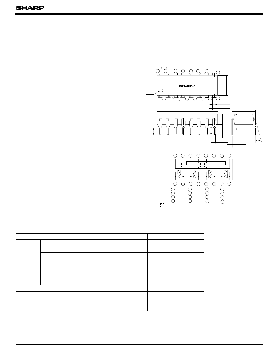
■ Features ■ Outline Dimensions
±
0.25
1. Propagation delay time
(t, t
PHL PLH
: TYP. 0.75ms
)
2. High noise resistance type
(CM
, CML: TYP. 2kV/µs
H
)
3. High sensitivity
(I
: MAX. 1.5 mA
FLH
)
4. Bi-directional input, 4-channel type
2.54
1516
Primary
side
mark
12345678
1314
PC906
19.82
1112
±
0.5
■ Applications
1. Programmable controllers
■Absoulte Maximum Ratings
Parameter Symbol Unit
*1
Forward current
Input
Output
*1 Each channel
*2 Pulse width<=100µs, Duty ratio : 0.001
*3 All channel
*4 Shall not exceed from supply voltage (V
*5 40 to 60%RH, AC for 1min.
*6 For 10 seconds
*1, *2
Peak forward current
*1
Power dissipation
Supply voltage V
*1, *4
Output voltage
*1
Output current
*3
Power dissipation
*5
Isolation voltage
Operating temperature
Storage temperature
*6
Soldering temperature
)
CC
I
V
P
V
T
T
T
.
± 0.5
3.0
Internal connection diagram
123
V
1
IN1a
V
2
IN1b
V
3
IN2a
V
4
A:Light detecting portion + signal processing circuit
IN2b
456
5 V
IN3a
6 V
IN3b
V
7
IN4a
V
8
IN4b
* “OPIC ” (Optical IC) is a trademark of the SHARP Corporation.
An OPIC consists of a light-detecting element and signal processing circuit integrated onto a single chip.
(
Ta= 25˚C
Ratings
I
F
FM
±26 mA
±1 A
P40mW
CC
O
I
O
O
iso
opr
stg
sol
7V
7V
4mA
200 mW
4 000
V
rms
- 25 to + 85 ˚C
- 55 to + 125 ˚C
260 ˚C
10
9 V
10
11
12
±0.5
3.3
111213141516
V
GND
V
CC
O4
O3
9
±
0.9
±
1.2
± 0.1
0.5
10
AAAA
78
13
V
GND
14
V
15
V
16
(
Unit : mm
± 0.5
6.5
0.2
0.3
7.62
± 0.5
3.5
Epoxy resin
TYP.
0.5
0.26
θ
= 0 to 13˚
9
O2
O1
CC
±
)
±
0.3
θ
0.1
)
“ In the absence of confirmation by device specification sheets, SHARP takes no responsibility for any defects that occur in equipment using any of SHARP's devices, shown in catalogs,
data books, etc. Contact SHARP in order to obtain the latest version of the device specification sheets before using any SHARP's device.”
Page 2

PC906
■ Electro-optical Characteristics
Parameter Symbol
Input
Output
Transfer
characterisics
*7 All channel
*8 Maximum “ Peak to peak ” voltage of sine wave to keep Vo>=3.5V when it is superposed 100kHz sine wave to Vcc.
*9 Maximum “ Peak to peak ” voltage of sine wave to keep Vo<=4.0V when it is superposed 100kHz sine wave to Vcc.
*10 Maximum value which Vo can keep 0.4V MAX. when it inputs the pulse, I
Forward voltage V
Terminal capacitance
Operating supply voltage V
Low level output voltage V
High level output voltage V
Output short-circuit current
*7
Low level supply current
*7
High level supply current
*8
Power supply noise induction
“ Output high level ”
*9
Power supply noise induction
“Output low level”
“ Low→High” threshold input
current 1
“ Low→High” threshold input
current 2
*7
Isolation resistance
“ Low→High” propagation time
Response
time
“ High→Low”propagation time
Rise time t
Fall time t
Instantaneous common mode
rejection voltage
(
High level output
)
Instantaneous common mode
rejection voltage
(
Low level output
*10
Input terminal noise-proof
)
PSNI
PSNI
I
I
CM
CM
SNI
(
Shows characteristics value 1ch. at Vcc= 5V, Ta= 25˚C,
unless otherwise specified
Conditions MIN. TYP. MAX. Unit Fig.
= ± 10mA - 1.2 1.4 V
I
F
F
C
VF= 0, f= 1MHz
t
cc
= 0mA, IOL= 1.6mA - 0.1 0.4 V 1
I
F
OL
= ± 4mA 3.5 - - V 2
I
F
OH
= ± 4mA - 0.75 - 0.45 - 0.25 mA 3
I
F
IF= 0mA
I
= ± 4mA - 16 28 mA
F
R
= 4.0kΩ, IF= ± 4mA
L
H
f
= 100kHz
AC
= 4.0kΩ, IF= 0mA
R
L
L
f
= 100kHz
AC
R
= 4.0kΩ
L
DC500V, 40 to 60%RH
I
= ± 4mA
F
R
r
f
= 4.0kΩ
L
R
= 4.0kΩ, IF= ± 4mA
L
= 600V (peak
V
CM
H
(MIN.)= 2.0V
V
O
= 4.0kΩ, IF= 0mA
R
L
V
= 600V (peak
CM
L
(MAX.)= 0.8V
V
O
R
=4kΩ
F
L
I
I
R
t
t
I
OS
CCL
CCH
FLH1
FLH2
ISO
PLH
PHL
)
4.5 - 5.5 V
-1830mA
0.5 - - Vp - p
0.5 - - Vp - p
- 0.7 1.5 mA
- - 0.7 - 1.5
10
5x10
)
)
(1 cycle : 1ms and pulse width : 1µs).
F
1x10
- 0.75 1.35 ms
- 0.75 1.35 ms
- 0.3 0.7 µ s
- 0.05 0.4 µ s
--V/µs
- 2 000
--V/µs
2 000
10 - - mA 9
11
-- 30 250 pF
4
5
6
mA
--Ω
7
8
Page 3
■ Test circuit
Fig. 1 Fig. 2
PC906
PC906
PC906
I
F
Fig. 3
I
F
V
V
V
V
INa
INb
PC906
INa
INb
V
V
GND
V
V
GND
V
cc
o
V
cc
I
F
V
INa
V
INb
cc
V
o
V
V
cc
V
GND
Fig. 4
PC906
cc
o
V
cc
I
F
V
V
V
INa
INb
cc
V
o
A
V
cc
A
GND
Fig. 5
I
F
Fig. 6
PC906
PC906
I
V
V
GND
cc
R
L
o
CRT
V
cc
5V
f
AC
= 100kHz
V
INa
V
INb
F
V
INa
V
It measures the IF when output changes
from “ Low level” to “ High level ” .
V
cc
R
L
V
INb
o
0.1µ F
CRT
V
cc
GND
Page 4

PC906
Fig. 7
I
F
47Ω
PC906
V
V
INa
V
INb
cc
R
V
o
L
0.1µ F
CRT
V
cc
GND
Input
waveform
V
O
waveform
TT
t
PLH
(
Note) T >= 50ms
= ± 4mA
I
F
I
= 0mA
F
t
PHL
90%
1.5V
10%
t
r
t
f
Fig. 8
PC906
SW
A
B
V
V
V
INa
INb
cc
R
L
V
o
0.1µ F
CRT
V
cc
V
CM
CM
waveform
, V
H
O
waveform
SW at B, I
= ± 4mA
F
GND
CML, V
O
V
CM
+
-
waveform
SW at A, I
= 0mA
F
(
V
MAX.)= 0.8V
O
V
CM
(
V
MIN.)= 2.0V
O
(
peak
GND
V
GND
V
GND
)
OH
OL
Fig. 9
I
F
47Ω
PC906
Input
V
INa
V
INb
V
cc
R
L
V
o
0.1µ F
CRT
V
cc
GND
waveform
10ns
1µ s
10ns
1ms
90%
50%
10%
Page 5

PC906
■ Internal Equivalent Circuit Diagram (1ch.
Decoder
Q1Q2Q3Q4Q
U/D
U/D Counter
10kΩ
5
CK
Voltage regulator
Comparator
+
-
Oscillation
circuit
Fig. 1 Forward Current vs. Ambient
Temperature
50
40
)
mA
(
F
30
26
20
)
V
CC
V
O
GND
Fig. 2 Supply Current vs. Ambient
Temperature
I
CCL
(
= 0mA
I
)
mA
(
, I
CCH
CCL
20
15
10
F
(
I
F
VCC=5V
I
CCH
= ± 4mA
)
)
Forward current I
10
0
Ambient temperature Ta (˚C
50250-25 85
)
Fig. 3 Low Level Output Voltage vs.
Ambient Temperature
0.20
)
V
(
0.15
OL
0.10
0.05
Low level output voltage V
0
-25 0255075
Ambient temperature Ta (˚C
0255075
VCC=5V
I
= 0mA
F
I
= 1.6mA
OL
)
5
Supply current I
0
10075
-25
0255075
Ambient temperature Ta (˚C
100
)
Fig. 4 Relative Threshold Input Current vs.
Ambient Temperature
100
2.0
1.5
1.0
0.5
Relative threshold input current
0
-25
Ambient temperature T
V
R
I = 1 at
FLH
T
(˚C
a
CC
=4kΩ
L
= 25˚C
a
)
=5V
100
Page 6
PC906
Fig. 5 Propagation Delay Time vs.
Forward Current
F
(mA)
RL=4kΩ
= 25˚C
T
a
)
ms
(
1.0
PHL
, t
PLH
t
0.75
0.5
Propagation delay time t
Forward current I
, t
PLH
PHL
510
Fig. 7 Output Short-circuit Current vs.
Ambient Temperature
0
a
(˚C)
VCC=5V
= ± 4mA
I
F
- 0.1
)
- 0.2
mA
(
OS
- 0.3
- 0.4
- 0.5
- 0.6
- 0.7
Output short-circuit current I
- 0.8
-25
Ambient temperature T
0 25 50 75 100
Fig. 6 Propagation Delay Time vs.
Ambient Temperature
=5V
V
CC
= ± 4mA
)
ms
(
1.0
PHL
, t
PLH
t
, t
PLH
PHL
I
R
F
L
=4kΩ
0.75
0.5
Propagation delay time t
0
-25
150
0 25 50 75 100
Ambient temperature T
a
(˚C)
Fig. 8 Rise Time, Fall Time vs.
Load Resistance
=5V
V
CC
I
L
t
r
t
f
(kΩ)
= ± 4mA
F
T
= 25˚C
a
0.6
0.5
)
µs
(
f
0.4
, t
r
0.3
0.2
0.1
Rise time, fall time t
0
0.1 1 5 10 100
Load resistance R
Page 7

PC906
Fig. 9-a Supply Voltage/Output Voltage vs. Fig. 9-b Supply Voltage/Output Voltage vs.
Time (1
5
)
V
4
(
CC
3
2
Supply voltage V
1
0
0
5
)
V
4
(
O
3
2
Output voltage V
1
0
0
)
I
F
50 100
Time (ms
Time (ms
= 0mA
T
dVcc
dt
)
)
R
L
= 25˚C
a
= ± 0.1V/ms
=4kΩ
V
CC
V
O
Time (2
5
)
V
4
(
CC
3
2
Supply voltage V
1
0
0
5
)
V
4
(
O
3
2
Output voltage V
1
0
10050
0
)
IF= ± 4mA
dVcc
50 100
)
Time (ms
)
Time (ms
Ta= 25˚C
= ± 0.1V/ms
dt
R
=4kΩ
L
V
V
O
CC
10050
Please refer to the chapter “Precautions for Use ”.
●
 Loading...