

Page 1
Digital Output Type OPIC
PC900V/PC900VQ
❈ Lead forming type (I type) and taping reel type (P type) are also available. (PC900VI/PC900VP)
..
❈❈ TUV (DIN-VDE0884) approved type is also available as an option.
■ Features
1. High reliability type (PC900VQ
2. Normal OFF operation, open collector
output
3. TTL and LSTTL compatible output
4. Operating supply voltage V
5. High isolation voltage between input and
output (V
: 5 000V
iso
)
rms
6. Recognized by UL, file No. E64380
)
: 3 to 15V
CC
Photocoupler
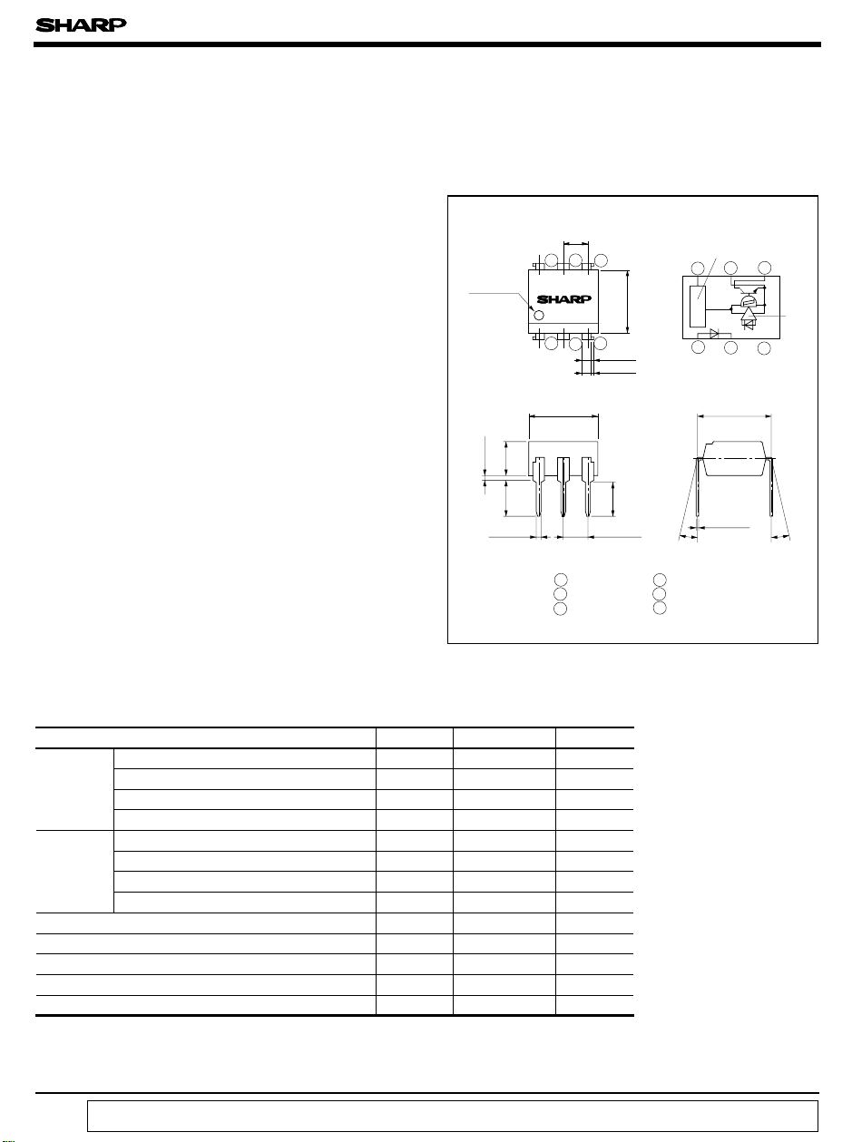
■ Outline Dimensions
± 0.25
2.54
Anode
mark
PC900V
456
123
0.9
1.2
± 0.5
± 0.2
± 0.3
6.5
PC900V/PC900VQ
(
Unit : mm
Internal connection
diagram
Voltage regulator
456
Amp
123
)
■ Applications
1. Isolation between logic circuits
2. Logic level shifters
3. Line receivers
4. Replacements for relays and pulse trans formers
5. Noise reduction
■ Absolute Maximum Ratings
Parameter Symbol Rating Unit
Forward current I
*1
Input
Output
*1 Pulse width<=100µs, Duty ratio : 0.001
*2 40 to 60% RH, AC for 1 minute
*3 For 10 seconds
Peak forward current I
Reverse voltage V
Power dissipation P 70 mW
Supply voltage V
High level output voltage V
Low level output current I
Power dissipation P
Total power dissipation P
*2
Isolation voltage V
Operating temperature T
Storage temperature T
*3
Soldering temperature T
± 0.5
0.5
7.12
± 0.5
TYP.
3.5
0.5
± 0.5
3.7
± 0.1
0.5
1 Anode
2 Cathode
3 NC
* “OPIC ” (Optical IC) is a trademark of the SHARP Corporation.
An OPIC consists of a light-detecting element and signal processing circuit integrated onto a single chip.
(
Ta= 25˚C
F
FM
R
CC
OH
OL
O
tot
iso
opr
stg
sol
50 mA
1A
6V
16 V
16 V
50 mA
150 mW
170 mW
5 000
- 25 to + 85 ˚C
- 40 to + 125 ˚C
260 ˚C
± 0.5
3.35
± 0.25
2.54
4 V
O
5 GND
6 V
CC
θ
)
V
rms
7.62
θ
= 0 to 13 ˚
0.26
± 0.3
± 0.1
θ
“ In the absence of confirmation by device specification sheets, SHARP takes no responsibility for any defects that occur in equipment using any of SHARP's devices, shown in catalogs,
data books, etc. Contact SHARP in order to obtain the latest version of the device specification sheets before using any SHARP's device.”
Page 2
PC900V/PC900VQ
■ Electro-optical Characteristics
Parameter
Forward voltage
Input
Reverse current
Terminal capacitance
Operating supply voltage
Low level output voltage
Output
High level output current
Low level supply current
High level supply current
*4
“High→Low ” threshold
input current
*5
“Low→High ” threshold
Transfer
charac-
teristics
*4 I
represents forward current when output goes from high to low.
FHL
represents forward current when output goes from low to high.
*5 I
FLH
*6 Hysteresis stands for I
*7 Test circuit for response time is shown below.
input current
*6Hysteresis
Isolation resistance
“ High→Low ”
“ Low→High ”
time
Fall time
Rise time
FLH/IFHL
Response
*7
propagation delay time
propagation delay time
.
<Precautions for Use>
Connect a capacitior of more than 0.1µF between VCC and GND.
Symbol
V
V
V
I
I
I
I
l
I
FLH/IFHL
R
t
t
= 4mA
I
F
F
= 0.3mA
I
F
I
Ta= 25˚C, V
R
C
Ta= 25˚C, V= 0, f = 1kHz
t
CC
= 16mA, VCC= 5V, IF= 4mA
I
OL
OL
= 15V, IF=0
V
OH
O=VCC
= 5V, IF= 4mA
V
CCL
CC
= 5V, IF=0
V
CCH
CC
Ta= 25˚C, V
FHL
FLH
PHL
PLH
t
t
ISO
f
r
= 5V, RL= 280 Ω
V
CC
Ta= 25˚C, V
= 5V, RL= 280 Ω
V
CC
= 5V, RL= 280 Ω
V
CC
Ta = 25˚C, DC500V, 40 to 60% RH
Ta= 25˚C
V
CC F
= 280Ω
R
L
Conditions
=3V
R
= 5V, RL= 280 Ω
CC
= 5V, RL= 280 Ω
CC
= 5V, I
(
Ta= 0 to + 70˚C unless specified
MIN. TYP. MAX. Unit
- 1.1 1.4
0.7 1.0 -
--10µA
- 30 250 pF
3 - 15 V
- 0.2 0.4 V
- - 100 µA
- 2.5 5.0 mA
- 1.0 5.0 mA
- 1.1 2.0
- - 4.0
0.4 0.8 -
0.3 - -
0.5 0.7 0.9 -
10
11
5x10
10
− 13
= 4mA
-26
- 0.05 0.5
- 0.1 0.5
)
V
mA
mA
- Ω
µs
t
= tf= 0.01 µ s
r
= 50 Ω
Z
O
Test Circuit for Response Time
Voltage
regulator
5V
280Ω
V
V
IN
47Ω
Amp
O
0.1µ F
V
IN
t
PHL
V
O
t
f
t
PLH
10%
t
50%
90%
r
V
V
OH
1.5V
OL
Page 3

PC900V/PC900VQ
Fig. 1 Forward Current vs. Ambient
Temperature
60
50
)
40
mA
(
F
30
20
Forward current I
10
0
- 25 0 25 50 75 10085
Ambient temperature T
)
(˚C
a
Fig. 3 Forward Current vs. Forward Voltage
500
= 75˚C
T
a
200
100
)
mA
(
50
F
20
10
5
Forward current I
2
1
0
50˚C
0.5 1.0 1.5 2.0 2.5 3.0
Forward voltage V
F
- 25˚C
(V
25˚C
0˚C
)
Fig. 5 Relative Threshold Input Current vs.
Ambient Temperature
1.6
VCC=5V
1.4
1.2
I
1.0
0.8
0.6
Relative threshold input current
0.4
0.2
FHL
I
FLH
I
= 1 at Ta= 25˚C
FHL
0 25 50 100-25 75
Ambient temperature Ta (˚C
)
Fig. 2 Power Dissipation vs. Ambient
Temperature
200
P
170
)
150
mW
(
tot
, P
O
100
50
Power dissipation P
0
-25
tot
P
O
0 25507510085
Ambient temperature T
a
(˚C
)
Fig. 4 Relative Threshold Input Current vs.
Supply Voltage
1.4
Ta= 25˚C
I
= 1 at VCC=5V
FHL
1.2
1.0
0.8
0.6
Relative threshold input current
0.4
0.2
I
FHL
I
FLH
510 20015
Supply voltage VCC (V
)
Fig. 6 Low Level Output Voltage vs.
Low Level Output Current
1.0
)
(
VCC=5V
0.5
T
V
OL
0.05
Low level output voltage V
0.02
0.01
= 25˚C
a
0.2
0.1
1
2 5 10 1005020
Low level output current IOL (mA
)
Page 4

PC900V/PC900VQ
Fig. 7 Low Level Output Voltage vs.
Ambient Temperature
0.5
I
)
(
VCC=5V
V
0.4
OL
0.3
0.2
0.1
Low level output voltage V
0
- 25 0 25 50 100
Ambient temperature Ta (˚C
OL
= 30mA
16mA
5mA
75
)
Fig. 9 Propagation Delay Time vs.
Forward Current
5
VCC=5V
)
µ s
(
, t
PLH
PHL
= 280Ω
R
L
T
= 25˚C
a
4
3
2
t
PLH
Fig. 8 Supply Current vs. Supply Voltage
9
8
7
)
mA
6
(
CC
5
4
3
Supply current I
2
I
{
CCL
1
{
I
CCH
0
59 17113
Supply voltage VCC (V
85˚C
85˚C
Ta= - 25˚C
25˚C
Ta= - 25˚C
25˚C
11 1573
)
Fig.10 Rise Time, Fall Time vs.
Load Resistance
0.5
VCC=5V
I
=4mA
F
T
= 25˚C
)
µ s
(
f
, t
r
a
0.4
0.3
0.2
t
r
Rise time, fall time t
1
Propagation delay time t
0
10 20 30 40 60050
Forward current IF (mA
t
PHL
)
0.1
0
0.2 0.5 1 2 5 10 20
0.1
Load resistance R
■ Precautions for Use
(1)
It is recommended that a by-pass capacitor of more than 0.01µ F is added
between V
(2)
Handle this product the same as with other integrated circuits against
static electricity.
• Please refrain from soldering under preheating and refrain from soldering by reflow.
Please refer to the chapter “Precautions for Use.”
●
and GND near the device in order to stabilize power supply line.
CC
t
f
)
(kΩ
L
 Loading...