

Page 1
1
- January 1998
Highlights
www.national.com
©
1998 National Semiconductor Corporation
PRELIMINARY
April 1998
PC87570 Keyboard and Power Management Controller
Highlights
General Description
The PC87570 is a highly integrated embedded RISC-based
controller optimized for power management (PM), keyboard
and mouse (KBC) and system control in portable Personal
Computer (PC) applications.
The PC87570 incorporates National’s CompactRISC
CR16A core, a high performance 16-bit RISC processor
core, a Bus Interface Unit (BIU) that directly interfaces with
memory and I/O devices, on-chip memory and system support functions. Among these are legacy functions, handled
by the Host Bus Interface (HBI), that include the Real-Time
Clock and Advanced Power Control (RTC and APC), and
peripherals, including: frequency-multiplier-based High Frequency Clock Generator (HFCG), Power Mode Control
(PMC), Interrupt Control Unit (ICU), Multi-Input Wake-Up
(MIWU), General Purpose I/O Ports (GPIO) with internal
keyboard matrix scanning, PS/2
®
Interface, ACCESS.bus
®
(ACB) Interface, two Multi-Function 16-Bit Timers (MFT16),
periodic interrupt timer and WATCHDOG (TWD), ADC
and DAC.
The PC87570 highly efficient architecture and its on-chip
peripherals, supporting functions and low power consumption, provide a highly integrated solution for portable notebook PCs, sub-notebook PCs and other portable devices.
Outstanding Features
●
Shared BIOS memory
●
Fully ACPI-compliant embedded controller
●
Proprietary PS/2 shift mechanism
●
Extremely low current consumption in Idle mode
●
Support for a variety of off-chip wake-up sources
●
Scalable design for growth without controller upgrade
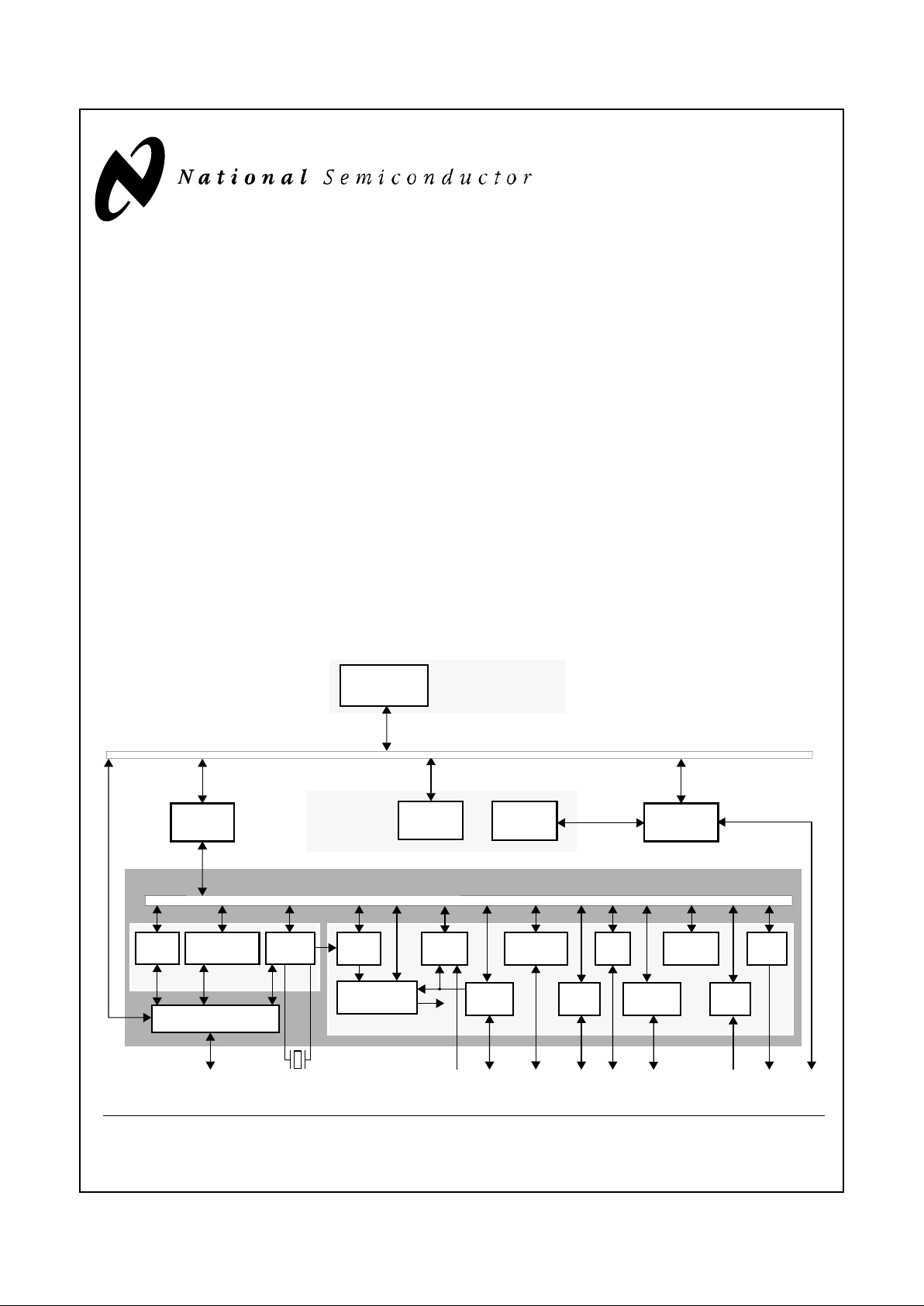
Block Diagram
Core Bus
Peripheral Bus
Bus
KBC + PM
Host I/F
RTC +
Processing
Unit
HBI
Host Bus
APC
Host
Config
RAM
Memory
External
BIU
CR16A Core
32.768
ICU
HFCG
PMC
ADC
KBSCAN
ACB
GPIO
WDG
Peripherals
Legacy
ROM
MIWU
IBM®, PC-AT® and PS/2® are registered trademarks of International Business Machines Corporation.
CompactRISC
TM
, WATCHDOGTM and TRI-STATE® are trademarks of National Semiconductor Corporation.
ACCESS.bus® is a registered trademark of Digital Equipment Corporation.
I
2C®
is a registered trademark of Philips.
Memory
(ISA Compatible)
MFT16
Timer +
KHz
Adapter
PS/2
I/F
I/F
CLK
DAC
+ I/O
(X2)
Page 2

2
Highlights
www.national.com
Features
• CR16A Core
— 16-bit embedded RISC processor core
• Bus Interface Unit (BIU)
— Three address zones for static devices (SRAM,
ROM FLASH, I/O)
— Configurable wait states and fast read bus cycles
• Internal Memory
— 2048 bytes of on-chip ROM
— 1024 bytes of on-chip RAM
— All memories can hold both code and data
• External Memory
— Supports BIOS memory (Flash) sharing with PC host
— Up to 56 Kbyte for code and data
— Field upgradable with Flash or SRAM devices
— Supports host controlled code download and update
• Host Bus Interface (HBI)
— Three host interface channels, typically used for the
KBC, PM and RTC devices
— Motherboard Plug and Play (PnP) configuration
o With Enable and Lock bits for each device
o Relocatable address for each device
— Host power supply indicator input pin
— 8042 KBC standard Interface (60h, 64h)
— Intel 80C51SL compatible
— IRQ1 and IRQ12 support
— Fast Gate A20 and Fast host Reset, via firmware
— PM interface port (62h, 66h)
— PM port IRQ11
• Real-Time Clock (RTC) and Advanced Power Control
(APC)
— RTC
o DS1287, MC146818 and PC87911 compatible
o 242 bytes battery backed-up CMOS RAM
o Calendar including century and automatic leap-
year adjustment
o Optional daylight saving adjustment
o BCD or binary format for timekeeping
o Three individually maskable interrupt event
flags: periodic rates from 122 µs to 500 ms; timeof-day alarm, once per second to once per day
o Separate backup battery pin
o Double buffer time registers
o The CMOS RAM and the RTC registers can be
accessed by the CR16A firmware
— APC
o Alarm wake-up
o Hardware wake-up events
o Software off events
• HFCG
— On-chip frequency multiplier
— Single 32.786KHz crystal
— Software controlled frequency generation
• PMC
— 3.3 and 5V operation with mixed voltage system
support
— Reduced power consumption capability
— Back-drive protection
— Three power modes, switched by software or hard-
ware:
o Active mode operating frequency 4-10MHz
o Idle (20 µA)
o Power Off - RTC only (0.9 µA typical) from back-
up battery
— Automatic wake-up on system events
• ICU
— 16 maskable interrupt sources
— Four general purpose external interrupt inputs
— Programmable trigger mode (level: high or low,
edge: falling or rising)
— Enable and pending indication for each interrupt
— Non-maskable interrupt input
• MIWU
— Supports up to 24 wake-up or interrupt inputs
— Generates wake-up to PMC
— Generates interrupts to ICU
— Provides user-selectable trigger conditions
• GPIO
— 76 ports
— I/O pins individually configured as input or output
— Configurable internal pull-up resistors
— Special ports for internal keyboard matrix scanning
o 16 open-collector outputs
o 8 Schmidt inputs with internal pull-up
— Special input for system On/Off switch
— Supports very low-cost implementation of additional
off-chip I/O ports
• PS/2 Interface
— Supports three independent devices (external KBC,
mouse and additional pointing device)
— Supports byte lev el handling via hardware accelerator
• ACB Interface
— Intel SMBus and Philips I
2C®
compatible
— ACCESS.bus master and slave
— Supports polling and interrupt controlled operation
— Generates a wake-up signal on detection of a Start
Condition, while in power-down mode
— Optional internal pull-up on SDA and SCL pins
Page 3
3
Highlights
www.national.com
• MFT16
— Two 16-bit timers
— Each timer supports Pulse Width Modulator (PWM),
Capture and Counter capabilities
• TWD
— 16-bit periodic interrupt timer with 30-µs resolution
and 5-bit prescaler, for system tick and periodic
wake-up tasks
— 8-bit WATCHDOG timer
• ADC
— Eight channels, 8-bit resolution
— 10 µs conversion/channel
— Internal or external voltage reference
• DAC
— Four channels, 8-bit resolution
— 1 µs conversion time for 50 pF load
— Full output range from AGND to AVCC
• Supports Microsoft Advanced Power Management
(APM) specifications revision 1.2, February 1996
— Generates the System Management Interrupt (SMI)
• 160-pin PQFP and 176-pin TQFP packages
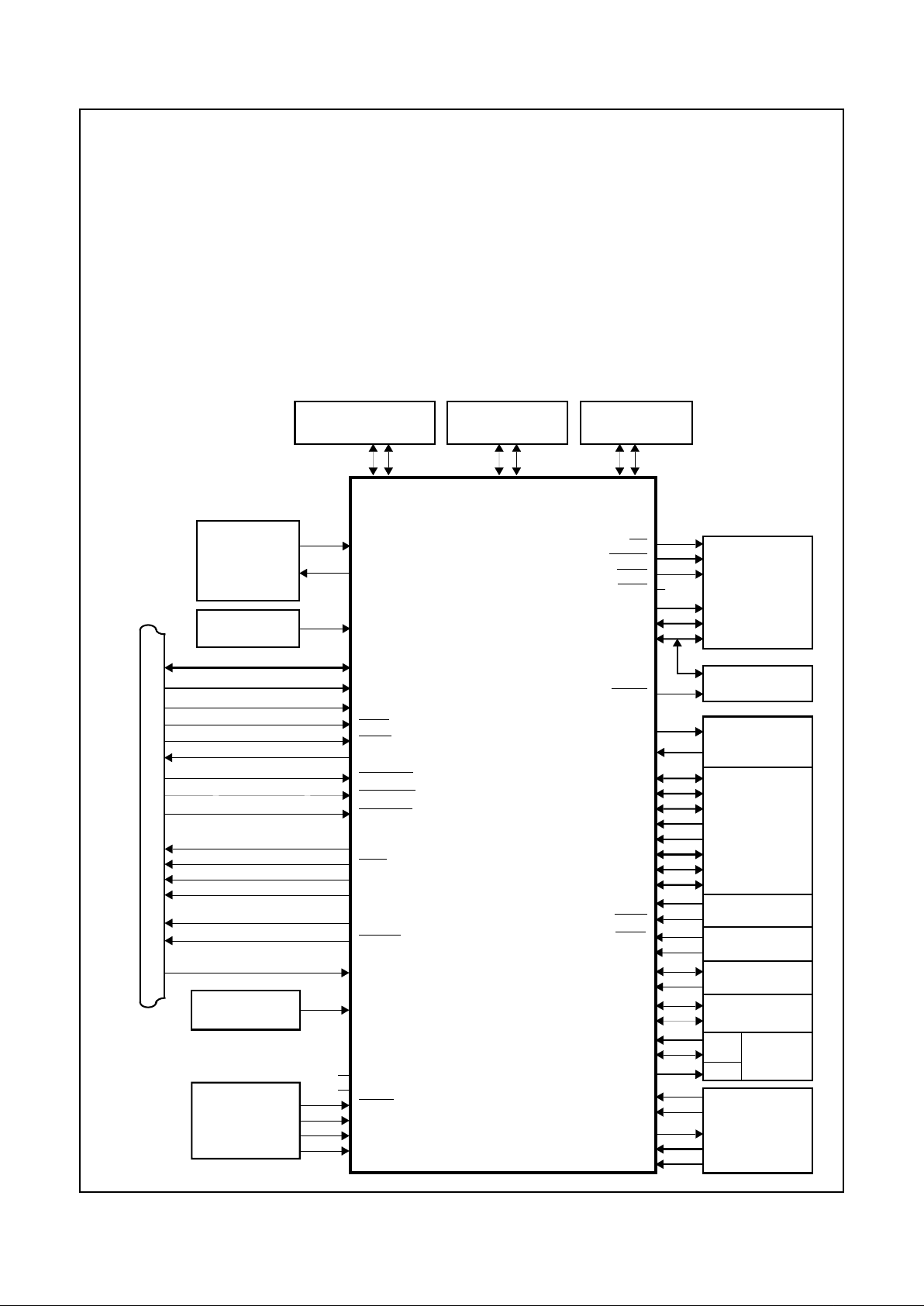
Basic Configuration
or
Clock
External
Memory
PC87570
Host System Bus (ISA Compatible)
32KX1/32KCLKIN
32KX2
HMR
HA18-0
HD7-0
HIOR
HIOW
IRQ1
IRQ11
IRQ12
RD
WR1-0
SEL0
A18-16, A15-0
D15-8
AD7-0
DA3-0
PA6-0
PB7-0
PC7-0
PD7-0
HIOCHRDY
RTC
Battery
V
BAT
IRQ8
PSCLK1
PSDAT1
Crystal
32.768 KHz
External Keyboard
Internal
Keyboard
KBSOUT15-0
KBSIN7-0
SRAM or
Flash
ENV0
GA20
AVCC
AGND
VCC
GND
Power
Supply
SCL
D7-0
HMEMRD
HMEMWR
PSCLK2
PSDAT2
PSCLK3
PSDAT3
PG4-0
PE1-0
PF7-0
PH5-0
HMEMCS
HAEN
EXINT0,10,11,15
PFAIL
RING
SHBM
HRMS
Configuration
Inputs
I/O
Expansion
TA
HDEN
TRIS
HPWRON
PC0
External Mouse
Auxiliary PS/2
Interface
Interface
Interface
HRSTO
SELIO
(Matrix)
SDA
TB
SWIN
Analog
Reset
Control
(power-up reset)
GPIO
Interrupt
ACCESS.bus
System
Timers
ENV1
NC
NC
SEL1
NC
(Application)
V
REF
ADC
DAC
Page 4

4
Table of Contents
www.national.com
Table of Contents
Highlights.......................................................................................................................................................1
1.0 Introduction
1.1 INTERNAL ARCHITECTURE ....................................................................................................14
1.1.1 Processing Unit ...........................................................................................................14
1.1.2 BIU ...............................................................................................................................14
1.1.3 Memory ........................................................................................................................14
1.1.4 HBI ...............................................................................................................................14
1.1.5 Peripherals ..................................................................................................................14
1.2 EXPANSION OPTIONS .............................................................................................................15
1.3 OPERATING ENVIRONMENTS ................................................................................................15
1.3.1 IRE Environment .........................................................................................................16
1.3.2 IRD Environment .........................................................................................................17
1.3.3 DEV Environment ........................................................................................................18
2.0 Signal/Pin Connection and Description
2.1 CONNECTION DIAGRAMS ......................................................................................................19
2.2 SIGNAL/PIN DESCRIPTIONS ...................................................................................................21
2.3 RESET SOURCES AND TYPES ...............................................................................................26
2.3.1 Power-Up Reset ..........................................................................................................26
2.3.2 Warm Reset .................................................................................................................26
2.3.3 WATCHDOG Reset .....................................................................................................26
2.3.4 Triggering Reset ..........................................................................................................26
2.4 STRAP PINS ............................................................................................................................26
2.4.1 Setting the Environment ..............................................................................................26
2.4.2 Other Strap Pin Settings ..............................................................................................26
2.4.3 System Load on Strap Pins .........................................................................................27
2.4.4 Strap Inputs During Idle Mode .....................................................................................27
2.4.5 Strap Pin Status Register (STRPST) ...........................................................................27
2.5 ALTERNATE FUNCTIONS ........................................................................................................27
2.6 SYSTEM CONFIGURATION REGISTERS ...............................................................................29
2.6.1 Module Configuration Register (MCFG) ......................................................................29
2.6.2 PAGE Register ............................................................................................................30
2.7 SHARED MEMORY CONFIGURATION ...................................................................................30
2.8 MEMORY MAP ..........................................................................................................................30
2.8.1 Accessing Base Memory .............................................................................................31
2.8.2 Accessing External Memory ........................................................................................32
2.8.3 Accessing I/O Expansion Space .................................................................................33
3.0 Bus Interface Unit (BIU)
3.1 FEATURES ................................................................................................................................34
3.2 FUNCTIONAL DESCRIPTION ..................................................................................................34
3.2.1 Interfacing ....................................................................................................................34
3.2.2 Static Memory and I/O Support ...................................................................................34
Page 5

5
Table of Contents
www.national.com
3.2.3 Byte Accessing ............................................................................................................34
3.3 CLOCK AND BUS CYCLES ......................................................................................................34
3.3.1 Clock Cycles ................................................................................................................34
3.3.2 Control Signals ............................................................................................................35
3.3.3 Early Write Bus Cycle ..................................................................................................36
3.3.4 Late Write Bus Cycle ...................................................................................................38
3.3.5 Normal Read Bus Cycle ..............................................................................................40
3.3.6 Fast Read Bus Cycle ...................................................................................................42
3.3.7 I/O Expansion Bus Cycles ...........................................................................................43
3.3.8 I/O Expansion Example ...............................................................................................44
3.4 DEVELOPMENT SUPPORT .....................................................................................................44
3.4.1 Bus Status Signals ......................................................................................................44
3.4.2 Core Bus Monitoring ....................................................................................................44
3.5 BIU REGISTERS .......................................................................................................................45
3.5.1 BIU Configuration Register (BCFG) ............................................................................45
3.5.2 I/O Zone Configuration Register (IOCFG) ...................................................................45
3.5.3 Static Zone Configuration Register (SZCFGn) ............................................................45
3.6 USAGE HINTS ..........................................................................................................................46
4.0 On-Chip Memory
4.1 INTERNAL RAM ........................................................................................................................47
4.2 INTERNAL ROM ........................................................................................................................47
4.2.1 Access Times ..............................................................................................................47
4.2.2 ROM Shadow ..............................................................................................................47
5.0 Host Bus Interface (HBI)
5.1 FEATURES ................................................................................................................................48
5.2 HOST ACCESS TO SHARED MEMORY DEVICE ...................................................................49
5.2.1 Enabling Shared Memory Mode ..................................................................................49
5.2.2 Memory Device Interface .............................................................................................49
5.2.3 Host Access to Shared Memory ..................................................................................49
5.3 CORE ACCESS TO RTC/APC ..................................................................................................49
5.3.1 Host and CR16A Arbitration over RTC/APC ...............................................................49
5.4 USAGE HINTS ..........................................................................................................................49
5.4.1 Shared Memory ...........................................................................................................49
5.4.2 Wake-Up from Host .....................................................................................................50
5.4.3 Host Power-on Indication ............................................................................................50
5.5 HOST ACCESS TO PC87570 RESIDENT I/O DEVICES .........................................................50
5.5.1 Host Access to Configuration Registers ......................................................................50
5.5.2 Host Access to Resident I/O Devices ..........................................................................50
5.5.3 Host Bus I/O Cycles ....................................................................................................50
5.6 KBC CHANNEL .........................................................................................................................50
5.6.1 Status Register ............................................................................................................50
5.6.2 DBBOUT Register .......................................................................................................51
5.6.3 DBBIN Register ...........................................................................................................51
Page 6

6
Table of Contents
www.national.com
5.7 PM CHANNEL ...........................................................................................................................52
5.8 RTC/APC CHANNEL .................................................................................................................52
5.9 CR16A INTERRUPTS ...............................................................................................................52
5.10 HOST INTERRUPTS .................................................................................................................52
5.10.1 IRQ1, IRQ12 and IRQ11 and IRQ8 Buffers .................................................................53
5.11 SYSTEM CONSIDERATIONS ...................................................................................................53
5.11.1 Reset Configuration .....................................................................................................53
5.11.2 Host Power-On (HPWRON) Indication Input ...............................................................53
5.11.3 Host Master Reset (HMR) Input ..................................................................................53
5.11.4 Host Reset Output (HRSTO) from PC87570 ...............................................................53
5.11.5 HDEN Strap .................................................................................................................54
5.11.6 GA20 Pin Functionality ................................................................................................54
5.11.7 Host Driven Wake-Up ..................................................................................................54
5.11.8 APC-ON and APC-OFF Events ...................................................................................54
5.12 HBI REGISTERS ACCESSED BY CR16A ................................................................................54
5.12.1 Control and Status Register 1 (CST1) .........................................................................55
5.12.2 Control and Status Register 2 (CST2) .........................................................................55
5.12.3 RTC Core Address Register (RTCCA) ........................................................................55
5.12.4 RTC Core Data Register (RTCCD) .............................................................................56
5.12.5 Host PnP Initial Configuration Base Address Low and High Registers (HCFGBAL/H) 56
5.12.6 Host Interface Control Register (HICTRL) ...................................................................56
5.12.7 Host Interface IRQ Control Register (HIIRQC) ............................................................56
5.12.8 Host Interface KBC Status Register (HIKMST) ...........................................................57
5.12.9 Host Interface Keyboard Data Out Buffer Register (HIKDO) .......................................57
5.12.10 Host Interface Mouse Data Out Buffer Register (HIMDO) ...........................................58
5.12.11 Host Interface KBC Data In Buffer Register (HIKMDI) ................................................58
5.12.12 Host Interface PM Port Status Register (HIPMST) ......................................................58
5.12.13 Host Interface PM Data Out Buffer Register (HIPMDO) ..............................................58
5.12.14 Host Interface PM Data In Buffer Register (HIPMDI) ..................................................58
5.13 HOST CHANNEL CONFIGURATION .......................................................................................58
5.13.1 Chip Base Address Initial Setting ................................................................................58
5.13.2 Operation Guidelines ...................................................................................................60
5.14 HBI REGISTERS ACCESSED BY HOST .................................................................................61
5.14.1 Identification Register (SID) .........................................................................................61
5.14.2 Identification Type Register (SIDT) .............................................................................61
5.14.3 Identification Revision Register (SIDR) .......................................................................61
5.14.4 Base Address High Register (SBAH) ..........................................................................61
5.14.5 Base Address Low Register (SBAL) ............................................................................61
5.14.6 RTC Chip Select Address High Register (RTCCSAH) ................................................61
5.14.7 RTC Chip Select Address Low Register (RTCCSAL) .................................................61
5.14.8 KBC Chip Select Address High Register (KBCCSAH) ................................................62
5.14.9 KBC Chip Select Address Low Register (KBCCSAL) .................................................62
5.14.10 PM Chip Select Address High Register (PMCSAH) ....................................................62
5.14.11 PM Chip Select Address Low Register (PMCSAL) .....................................................62
5.14.12 Function Enable Register (FER) ..................................................................................62
5.14.13 Function Lock Register (FLR) ......................................................................................63
Page 7

7
Table of Contents
www.national.com
5.14.14 IRQ Enable Register (IRQE) .......................................................................................63
6.0 Real-Time Clock (RTC) and Advanced Power Control (APC)
6.1 FEATURES ................................................................................................................................64
6.2 RTC FUNCTIONAL DESCRIPTION ..........................................................................................64
6.2.1 Host Bus Interface .......................................................................................................64
6.2.2 Core Bus Interface .......................................................................................................64
6.2.3 Bank Description .........................................................................................................64
6.2.4 Bank Accessing ...........................................................................................................64
6.2.5 RTC Clock Generation ................................................................................................64
6.2.6 Internal Oscillator .........................................................................................................65
6.2.7 External Oscillator .......................................................................................................65
6.2.8 Timing Generation .......................................................................................................65
6.2.9 Timekeeping ................................................................................................................66
6.2.10 Updating ......................................................................................................................66
6.2.11 Alarms .........................................................................................................................67
6.2.12 Power Supply ..............................................................................................................67
6.2.13 System Bus Lockout ....................................................................................................68
6.2.14 Power-Up Detection ....................................................................................................68
6.2.15 Oscillator Activity .........................................................................................................68
6.2.16 Interrupt Handling ........................................................................................................68
6.2.17 Battery-Backed Register Banks and RAM ...................................................................68
6.3 RTC REGISTERS ......................................................................................................................69
6.3.1 RTC Control Register A (CRA) ....................................................................................69
6.3.2 RTC Control Register B (CRB) ....................................................................................70
6.3.3 RTC Control Register C (CRC) ...................................................................................70
6.3.4 RTC Control Register D (CRD) ...................................................................................71
6.4 USAGE HINTS ..........................................................................................................................71
6.5 APC FUNCTIONAL DESCRIPTION ..........................................................................................71
6.5.1 Operation .....................................................................................................................71
6.5.2 User Selectable Parameters ........................................................................................71
6.5.3 System Power States ..................................................................................................71
6.5.4 System Power Switching Logic ...................................................................................72
6.5.5 APC-ON/APC-OFF Interrupt Signals ...........................................................................72
6.5.6 Entering Power States .................................................................................................72
6.5.7 Predetermined Wake-Up .............................................................................................72
6.5.8 Ring Signal Event ........................................................................................................72
6.6 APC REGISTERS ......................................................................................................................72
6.6.1 APC Control Register 1 (APCR1) ................................................................................73
6.6.2 APC Control Register 2 (APCR2) ................................................................................73
6.6.3 APC Status Register (APSR) ......................................................................................73
6.6.4 RAM Lock Register (RLR) ...........................................................................................73
6.7 REGISTER BANKS ...................................................................................................................74
7.0 High Frequency Clock Generator (HFCG)
7.1 FEATURES ................................................................................................................................76
Page 8

8
Table of Contents
www.national.com
7.2 FUNCTIONAL DESCRIPTION ..................................................................................................76
7.2.1 Setting Clock Frequency .............................................................................................76
7.2.2 Fast Clock Setting .......................................................................................................77
7.3 HFCG REGISTERS ...................................................................................................................77
7.3.1 HFCG Control Register (HFCGCTRL) ........................................................................77
7.3.2 HFCGM Low Value Register (HFCGML) .....................................................................77
7.3.3 HFCGM High Value Register (HFCGMH) ...................................................................77
7.3.4 HFCGN Value Register (HFCGN) ...............................................................................77
7.3.5 HFCGI Low Value Register (HFCGIL) .........................................................................78
7.3.6 HFCGI High Value Register (HFCGIH) .......................................................................78
8.0 Power Mode Control (PMC)
8.1 FEATURES ................................................................................................................................79
8.2 THE POWER MODES ...............................................................................................................79
8.3 SWITCHING BETWEEN POWER MODES ...............................................................................79
8.3.1 Decreasing Power Consumption .................................................................................79
8.3.2 Increasing Performance ..............................................................................................79
8.4 POWER MODE CONTROL REGISTER (PMCR) .....................................................................80
8.5 USAGE HINTS ..........................................................................................................................80
9.0 Interrupt Control Unit (ICU)
9.1 FEATURES ................................................................................................................................81
9.2 FUNCTIONAL DESCRIPTION ..................................................................................................81
9.2.1 NMI ..............................................................................................................................81
9.2.2 Maskable Interrupts .....................................................................................................81
9.2.3 Edge/Level and Polarity Selection ...............................................................................81
9.2.4 Pending Interrupts .......................................................................................................81
9.2.5 External Interrupt Inputs ..............................................................................................81
9.2.6 Interrupt Assignment ...................................................................................................81
9.3 ICU REGISTERS .......................................................................................................................82
9.3.1 NMI Status Register (NMISTAT) .................................................................................82
9.3.2 Power Fail Control Register (PFAIL) ...........................................................................82
9.3.3 Interrupt Vector Register (IVCT) ..................................................................................83
9.3.4 Interrupt Enable and Mask Register (IENAM) .............................................................83
9.3.5 Interrupt Pending Register (IPEND) ............................................................................83
9.3.6 Edge Interrupt Clear Register (IECLR) ........................................................................83
9.3.7 Edge/Level Trigger Configuration Register (IELTG) ....................................................83
9.3.8 Trigger Polarity Configuration Register (ITRPL) ..........................................................83
9.4 USAGE HINTS ..........................................................................................................................83
9.4.1 Initializing .....................................................................................................................83
9.4.2 Clearing .......................................................................................................................83
9.4.3 Nesting ........................................................................................................................83
10.0 Multi-Input Wake-Up (MIWU)
10.1 FEATURES ................................................................................................................................84
Page 9

9
Table of Contents
www.national.com
10.2 FUNCTIONAL DESCRIPTION ..................................................................................................84
10.2.1 Trigger Conditions .......................................................................................................86
10.2.2 Pending Flags ..............................................................................................................86
10.2.3 Input Enable ................................................................................................................86
10.2.4 Interrupts .....................................................................................................................86
10.2.5 Input Assignments .......................................................................................................86
10.3 MIWU REGISTERS ...................................................................................................................86
10.3.1 Edge Detection Register 1(WKEDG1) .........................................................................86
10.3.2 Edge Detection Register 2 (WKEDG2) ........................................................................86
10.3.3 Edge Detection Register 3 (WKEDG3) ........................................................................86
10.3.4 Pending Register 1 (WKPND1) ...................................................................................86
10.3.5 Pending Register 2 (WKPND2) ...................................................................................86
10.3.6 Pending Register 3 (WKPND3) ...................................................................................87
10.3.7 Wake-Up Enable Register 1 (WKEN1) ........................................................................87
10.3.8 Wake-Up Enable Register 2 (WKEN2) ........................................................................87
10.3.9 Wake-Up Enable Register 3 (WKEN3) ........................................................................87
10.3.10 Pending Clear Register 1 (WKPCL1) ..........................................................................87
10.3.11 Pending Clear Register 2 (WKPCL2) ..........................................................................87
10.3.12 Pending Clear Register 3 (WKPCL3) ..........................................................................87
10.4 USAGE HINTS ..........................................................................................................................87
11.0 General Purpose I/O (GPIO) Ports
11.1 FEATURES ................................................................................................................................88
11.2 FUNCTIONAL DESCRIPTION ..................................................................................................88
11.2.1 Output Buffer ...............................................................................................................88
11.2.2 Input Buffer ..................................................................................................................88
11.2.3 Open Drain ..................................................................................................................88
11.2.4 Weak Pull-Up ...............................................................................................................88
11.3 GPIO PORT REGISTERS .........................................................................................................89
11.3.1 Port Alternate Function Register (PxALT) ...................................................................89
11.3.2 Port Direction Register (PxDIR) ...................................................................................89
11.3.3 Port Data Out Register (PxDOUT) ..............................................................................89
11.3.4 Port Data In Register (PxDIN) .....................................................................................89
11.3.5 Port Weak Pull-up Register (PxWPU) .........................................................................89
12.0 PS/2 Interface
12.1 FEATURES ................................................................................................................................90
12.2 FUNCTIONAL DESCRIPTION ..................................................................................................90
12.2.1 Configuration ...............................................................................................................90
12.2.2 Shift Mechanism ..........................................................................................................90
12.2.3 Quasi-Bidirectional Drivers ..........................................................................................90
12.2.4 Interrupt Signals ..........................................................................................................91
12.2.5 Power Modes ...............................................................................................................91
12.3 SHIFT MECHANISM ENABLED ................................................................................................91
12.3.1 Reset ...........................................................................................................................91
12.3.2 Enable .........................................................................................................................91
Page 10

10
Table of Contents
www.national.com
12.3.3 General PS/2 Interface Operation ...............................................................................91
12.3.4 Transmit Mode .............................................................................................................93
12.4 SHIFT MECHANISM DISABLED ...............................................................................................94
12.4.1 Clock Signal Control ....................................................................................................94
12.4.2 Data Signal Control .....................................................................................................94
12.4.3 Interrupt Generation ....................................................................................................94
12.5 PS/2 INTERFACE REGISTERS ................................................................................................95
12.5.1 PS/2 Data Register (PSDAT) ......................................................................................95
12.5.2 PS/2 Status Register (PSTAT) ....................................................................................95
12.5.3 PS/2 Control Register (PSCON) ..................................................................................95
12.5.4 PS/2 Output Signal Register (PSOSIG) ......................................................................96
12.5.5 PS/2 Input Signal Register (PSISIG) ...........................................................................96
12.5.6 PS/2 Interrupt Enable Register (PSIEN) ......................................................................96
13.0 ACCESS.bus (ACB) Interface
13.1 FEATURES ................................................................................................................................98
13.2 ACB PROTOCOL OVERVIEW ..................................................................................................98
13.2.1 ACB Interface ..............................................................................................................98
13.2.2 Data Transactions .......................................................................................................98
13.2.3 Start and Stop ..............................................................................................................98
13.2.4 Acknowledge Cycle .....................................................................................................98
13.2.5 “Acknowledge after every byte” Rule ...........................................................................99
13.2.6 Addressing Transfer Formats ....................................................................................100
13.2.7 Arbitration on the Bus ................................................................................................100
13.3 FUNCTIONAL DESCRIPTION ................................................................................................100
13.3.1 Master Mode ..............................................................................................................100
13.3.2 Slave Mode ................................................................................................................101
13.3.3 Power-Down ..............................................................................................................102
13.3.4 SDA and SCL Pin Configuration ................................................................................102
13.3.5 ACB Clock Frequency Configuration .........................................................................102
13.4 ACB REGISTERS ....................................................................................................................102
13.4.1 ACB Serial Data Register (ACBSDA) ........................................................................102
13.4.2 ACB Status Register (ACBST) ..................................................................................102
13.4.3 ACB Control Status Register (ACBCST) ...................................................................103
13.4.4 ACB Control Register 1 (ACBCTL) ............................................................................104
13.4.5 ACB Own Address Register (ACBADDR) .................................................................104
13.4.6 ACB Control Register 2 (ACBCTL2) ..........................................................................104
13.5 USAGE HINTS ........................................................................................................................105
14.0 Multi-Function 16-Bit Timer (MFT16)
14.1 FEATURES ..............................................................................................................................106
14.2 FUNCTIONAL DESCRIPTION ................................................................................................106
14.3 CLOCK SOURCE UNIT ...........................................................................................................107
14.3.1 Prescaler ...................................................................................................................107
14.3.2 External Event Clock .................................................................................................107
14.3.3 Pulse Accumulate Mode ............................................................................................107
Page 11

11
Table of Contents
www.national.com
14.3.4 Slow Speed Clock .....................................................................................................107
14.3.5 Counter Clock Source Select ....................................................................................108
14.4 TIMER/COUNTER AND ACTION UNIT ..................................................................................108
14.4.1 Operation Modes .......................................................................................................108
14.4.2 Timer Interrupts .........................................................................................................113
14.4.3 Timer I/O Functions ...................................................................................................113
14.5 MFT16 REGISTERS ................................................................................................................114
14.5.1 Clock Prescaler Register (TPRSC) ...........................................................................114
14.5.2 Clock Unit Control Register (TCKC) ..........................................................................114
14.5.3 Timer/Counter Register 1 (TCNT1) ...........................................................................114
14.5.4 Timer/Counter Register 2 (TCNT2) ...........................................................................114
14.5.5 Reload/Capture Register A(TCRA) ...........................................................................114
14.5.6 Reload/Capture Register B (TCRB) ..........................................................................114
14.5.7 Timer Mode Control Register (TCTRL) .....................................................................114
14.5.8 Timer Interrupt Control Register (TICTL) ...................................................................115
14.5.9 Timer Interrupt Clear Register (TICLR) .....................................................................115
15.0 Timer and WATCHDOG (TWD)
15.1 FEATURES ..............................................................................................................................116
15.2 FUNCTIONAL DESCRIPTION ................................................................................................116
15.2.1 Input Clock .................................................................................................................116
15.2.2 Pre-Scale ...................................................................................................................116
15.2.3 TWD Timer 0 .............................................................................................................116
15.3 WATCHDOG OPERATION ....................................................................................................117
15.4 TWD CONTROL AND CONFIGURATION ..............................................................................117
15.5 OPERATION IN IDLE MODE ..................................................................................................117
15.6 TWD REGISTERS ...................................................................................................................117
15.6.1 Timer and WATCHDOG Configuration Registers (TWCFG) .....................................117
15.6.2 Timer and Watchdog Clock Pre-Scaler Register (TWCP) .........................................117
15.6.3 TWD Timer 0 Register (TWDT0) ...............................................................................118
15.6.4 TWDT0 Control and Status Register (T0CSR) ..........................................................118
15.6.5 WATCHDOG Count Register (WDCNT) ...................................................................118
15.6.6 WATCHDOG Service Data Match Register (WDSDM) .............................................118
15.7 USAGE HINTS ........................................................................................................................118
16.0 Analog to Digital Converter (ADC)
16.1 FEATURES ..............................................................................................................................119
16.2 FUNCTIONAL DESCRIPTION ................................................................................................119
16.2.1 Reset .........................................................................................................................120
16.2.2 Reference Voltage .....................................................................................................120
16.2.3 Input Signal Range ....................................................................................................120
16.2.4 ADC Clock .................................................................................................................120
16.2.5 Initializing and Enabling the ADC ..............................................................................120
16.2.6 ADC Operation ..........................................................................................................121
16.2.7 Disabling the ADC to Save Power .............................................................................121
Page 12

12
Table of Contents
www.national.com
16.2.8 Sampling Time ...........................................................................................................121
16.2.9 Polling Driven Operation ............................................................................................121
16.2.10 Interrupt Driven Operation .........................................................................................121
16.2.11 Overflow ....................................................................................................................121
16.3 OPERATION MODES .............................................................................................................122
16.4 ADC REGISTERS ...................................................................................................................123
16.4.1 ADC Status Register (ADCST) ..................................................................................123
16.4.2 ADC Control Register 1 (ADCCNT1) .........................................................................123
16.4.3 ADC Control Register 2 (ADCCNT2) .........................................................................123
16.4.4 ADC Control Register 3 (ADCCNT3) .........................................................................124
16.4.5 ADC Data Registers ..................................................................................................125
16.5 USAGE HINTS ........................................................................................................................125
16.5.1 Power Supply and Layout Guidelines ........................................................................125
16.5.2 Power Consumption ..................................................................................................125
16.5.3 Filtering the Noise on Input Signals ...........................................................................126
16.5.4 AD0-7 Multiplexing with PD0-7 Port ..........................................................................126
16.5.5 Calculating the Sampling Time ..................................................................................126
17.0 Digital to Analog Converter (DAC)
17.1 FEATURES ..............................................................................................................................127
17.2 FUNCTIONAL DESCRIPTION ................................................................................................127
17.2.1 DAC Reset .................................................................................................................127
17.2.2 Reference Voltage .....................................................................................................127
17.2.3 Output Signal Range .................................................................................................127
17.2.4 Initializing and Enabling the DAC ..............................................................................128
17.2.5 Disabling the DAC .....................................................................................................128
17.2.6 Conversion Start ........................................................................................................128
17.3 DAC REGISTERS ...................................................................................................................128
17.3.1 DAC Control Register (DACCTRL) ............................................................................128
17.3.2 DAC Data Registers ..................................................................................................128
17.4 USAGE HINTS ........................................................................................................................128
17.4.1 Power Supply and Layout Guidelines ........................................................................128
17.4.2 Output Settling Time ..................................................................................................129
17.4.3 Output Voltage Accuracy ...........................................................................................129
17.4.4 Filtering Noise on Output Signals ..............................................................................129
17.4.5 Current Consumption ................................................................................................129
17.4.6 Entering Idle Mode ....................................................................................................129
18.0 Development System Support
18.1 ISE INTERRUPT .....................................................................................................................130
18.2 TRIS STRAP INPUT PIN .........................................................................................................130
18.3 FREEZING EVENTS ...............................................................................................................130
18.3.1 Disabling Maskable Interrupts ...................................................................................130
18.3.2 Freezing the WATCHDOG Counter ..........................................................................130
18.3.3 Disabling Additional Modules ....................................................................................130
18.3.4 Disabling Destructive Reads .....................................................................................130
Page 13

13
Table of Contents
www.national.com
18.4 MONITORING ACTIVITY DURING DEVELOPMENT .............................................................130
18.4.1 The Bus Status Signals .............................................................................................130
18.4.2 Transaction Effects on the External Bus ...................................................................130
18.4.3 Pipe Status Signals ...................................................................................................131
18.5 DEVELOPMENT SYSTEM REGISTERS ................................................................................131
18.5.1 Debug Configuration Register (DBGCFG) ................................................................131
18.5.2 Debug Freeze Enable Register (DBGFRZEN) ..........................................................131
19.0 Device Specifications
19.1 POWER AND GROUNDING ...................................................................................................132
19.2 GENERAL DC ELECTRICAL CHARACTERISTICS ...............................................................132
19.2.1 Recommended Operating Conditions .......................................................................132
19.2.2 Absolute Maximum Ratings .......................................................................................133
19.2.3 Power Supply Current under Recommended Operating Conditions .........................133
19.3 DC ELECTRICAL CHARACTERISTICS .................................................................................134
19.3.1 Analog .......................................................................................................................134
19.3.2 Digital .........................................................................................................................135
19.4 AC ELECTRICAL CHARACTERISTICS ..................................................................................137
19.4.1 Definitions ..................................................................................................................137
19.4.2 Timing Tables ............................................................................................................138
19.5 TIMING DIAGRAMS ................................................................................................................144
19.5.1 General ......................................................................................................................144
19.5.2 BIU .............................................................................................................................146
19.5.3 GPIO Ports ................................................................................................................149
19.5.4 Host Interface ............................................................................................................150
19.5.5 MFT16 .......................................................................................................................151
19.5.6 ACCESS Bus Interface ..............................................................................................152
19.5.7 Dev Environment Support .........................................................................................153
19.5.8 Interrupts and Wake-up .............................................................................................153
19.5.9 Reset .........................................................................................................................154
19.5.10 Host Power-on ...........................................................................................................154
19.5.11 PS/2 Interface ............................................................................................................155
A. CR16A Register Map
B. Bootloader Description
B.1 OVERVIEW .............................................................................................................................164
B.2 CONFIGURATION BLOCKS ...................................................................................................164
B.2.1 System Configuration Block ......................................................................................164
B.2.2 KBC Header ..............................................................................................................164
B.3 SYSTEM RESOURCES USED BY BOOTLOADER ...............................................................164
B.3.1 GPIO Pins ..................................................................................................................164
B.3.2 On-Chip RAM ............................................................................................................165
B.4 BOOTLOADER PROGRAM OPERATION ..............................................................................165
Page 14

Introduction
14
1.0 Introduction
www.national.com
1.0 Introduction
1.1 INTERNAL ARCHITECTURE
The following descriptions are based on the block diagram
in Highlights on page 1.
1.1.1 Processing Unit
The CompactRISC CR16A core is an advanced, generalpurpose, 16-bit microprocessor core with a RISC architecture. The core is responsible for arithmetic and logic operations and program control. For more details about the core
structure and instruction set, see
CR16A Core Architecture
Specification, Revision 1.1, January 1996.
1.1.2 BIU
The BIU controls access to:
●
on-chip Base Memory (boot-code, ZONE1, maskROM)
●
off-chip devices:
— Base Memory (boot-code, ZONE1, Flash or ROM)
— External Memory (application code, ZONE0, Flash
or SRAM)
— I/O Expansion
Each of these memories is associated with a ZONE in the
BIU. The zone configuration registers control access to devices connected to it. See Section 3.2 on page 34 for more
details on BIU.
1.1.3 Memory
ROM The on-chip ROM holds the CR16A boot program which
is run by the PC87570 upon reset (internal power-up reset, or
pulse on HMR pin). The 2048 byte on-chip ROM is used for
boot and External Memory update programs.
The boot program verifies that the External Memory exists
and holds a valid code; then, it jumps to execute this code.
If the External Memory does not hold a valid code (for example, the Flash is wrongly programmed), the boot program enables the host to download the code via the host
interface channel, and re-program the Flash.
The External Memory holds most of the PC87570 application
programs and constant data. The external memory can be any
kind of memory device since the PC87570 can directly interface with Flash, ROM or SRAM devices. This allows upgrading of the PC87570 firmware (keyboard controller code) in the
field.
RAM The 1024 byte on-chip RAM is mostly used for the
storage of program variables and stack. It can store short
programs used upon returning from Idle mode to Active
mode, and is preserved as long as VCC power is applied to
the PC87570. The PC87570 hardware arbitrates Flash usage by the CR16A firmware and the host processor BIOS
program, when the "shared-memory" configuration is used.
To reduce resource contention when this shared BIOS
Flash scheme is used, the host processor should copy the
Flash contents to the host’s main memory (DRAM) upon
system boot. Flash sharing is based on “cycle stealing” so
both the host processor and the CR16A can execute in parallel code from the same memory device.
1.1.4 HBI
The Host Bus Interface (HBI) bridges and arbitrates between host and CR16A accesses to shared resources. The
HBI allows the host and CR16A to share Flash memory.
See Section 5.2 on page 49 for more details on the shared
memory system.
The HBI enables host access to the KBD/MOUSE and the PM
interface ports, and to the RTC/APC. It also enables the
CR16A to access the RTC/APC and its CMOS RAM.
The host interface uses an ISA compatible bus protocol.
The PC87570 decodes the 16 ISA address lines to identify
the on-chip I/O device address as defined in the host configuration. Shared BIOS memory accesses to the device
are indicated by a memory chip select input from the host
(
HMEMCS signal), and three additional address lines (A16,
A17 and A18).
The Host Interface Configuration allows the host pro-
cessor to configure the interface to the PC87570 I/O devices (KBD, PM and RTC/APC host interface channels). The
Host Interface Configuration includes a motherboard Plugand-Play protocol that allows settings, such as the address
of each device, to be enabled and disabled. It also includes
a locking scheme to allow the BIOS program to protect the
configuration from tampering.
The Host Interface has three channels as follows:
●
Keyboard and Mouse (host addresses 60h, 64h).
●
Power Management (host address 62h, 66h)
●
RTC/APC (host address 70h, 71h).
The Host Interface supports the four legacy (ISA) interrupts.The PC87570 can generate interrupt requests to the
host processor via IRQ1, IRQ12, IRQ11 and
IRQ8 for the
Keyboard, Mouse, PM and RTC/APC handlers, respectively. This allows the PC87570 to be used with polling or interrupt driven schemes.
The PC87570 communicates with a host processor over an
ISA compatible, host interface bus. The KBD, PM and the
RTC/APC are interfaced as I/O devices over the I/O address space of the host.
In addition, the PC87570 generates the gate A20 control
signal (GA20 pin) and a soft reset signal (
HRSTO pin) to the
host. Optionally, this
HRSTO reset signal can be used to
prevent the host from accessing the shared Flash when the
PC87570 cannot perform the shared memory access during the PC87570’s boot-up time.
1.1.5 Peripherals
The RTC/APC has a low-power clock that provides time-of-
day, a calendar with century counter and alarm features. It
can work from either V
CC
or a backup battery using an internal switch. Other features include three maskable interrupt sources and 242 bytes of general-purpose RAM. An
external battery source maintains valid RAM and time during V
CC
failure. The RTC is software compatible with the
DS1287 and MC146818.
The APC hardware, with APM 1.2 compatible power con-
trol, features such as alarm wake-up, ring detection and
host control off commands. The APC controls the PC power
supply via the CR16A firmware. This allows maximum flexibility in designing an ACPI system based on the PC87570.
Page 15

Introduction
EXPANSION OPTIONS
15
www.national.com
The HFCG (High Frequency Clock Generator) provides
clocks for the various on-chip modules. These clocks are
generated directly from a 32.768 KHz crystal or from the onchip HFCG. The HFCG generates the high-frequency clock
using the RTC’s 32.768 KHz clock signal as a reference.
The PC87570 operation frequency is set by programming
the HFCG registers. The PMC enables and disables high
frequency clock generation, according to the required power mode.
The PMC (Power Mode Control) reduces the PC87570's
power consumption to the required activity level. Power
consumption is adjusted by controlling the clock frequency
and selective enabling/disabling of three power modes: Active, Idle and Power Off. Activity can be resumed by a periodic wake-up or via external events.
The ICU (Interrupt Control Unit) is a sixteen-channel module that interfaces between the interrupt requests (from different on-chip modules and external sources), and the
CR16A core. Both maskable and non-maskable interrupts
are generated.
For maskable interrupts, the ICU controls the masking of
the various sources and prioritizes the different requests. It
generates an interrupt to the core and indicates which of the
sources requested service. For non-maskable interrupts, it
combines the various sources into one and indicates which
is the requested service.
MIWU The Multi-Input Wake-Up module allows the device
to return from Idle mode. The CR16A can enable or disable
the various wake-up conditions. The PC87570 has a total of
23 wake-up signals, some of which are grouped to generate
a single interrupt signal.
GPIO Ports consist of up to 76 GPIO signals that provide
interface and control for the PC system. Some of these I/O
port signals share their pins with an alternate function (see
Table 2-5 on page 27), and may be mutually exclusive.
Some of these signals, when configured as inputs, can interrupt the CR16A when an event is detected even if the device is in Idle Mode. An example is the SWIN input, which is
dedicated for the PC’s On/Off switch.
One of the I/O pin can be used as an SMI output to the host
processor. The SMI is generated based on various events
identified by the CR16A. This includes an OFFcommand indication from the APC.
Internal keyboard scanning is supported by 16 open-drain
output port signals, and 8 input port signals with Schmidt
trigger input buffer and internal pull-up resistors. For power
efficiency, the inputs include an interrupt and a wake-up capability, so that pressing/releasing keys may be identified
without scanning the keyboard matrix in either Active or Idle
modes. The keyboard interrupt is controlled by the MIWU.
The PS/2 Interface, is an industry-standard, with PS/2compatible keyboard support, is implemented through a
two-wire, bidirectional TTL interface. Several vendors also
supply PS/2 mouse products and other pointing devices
with the same type of interface.
The PC87570 supports three PS/2 channels. Each channel
has two quasi-bidirectional signals which may be interfaced directly to an external keyboard, mouse or any other PS/2 compatible pointing device. Since the three channels are identical,
the connector ports are interchangeable.
The PC87570 includes a hardware accelerator that allows
the PS/2 channels to be controlled with minimal software
overhead. It also eliminates the sensitivity to interrupt latency that characterized traditional solutions.
The ACB Interface is a two-wire serial interface compatible with the ACCESS.bus physical layer. It is also compatible with Intel’s SMBus and Philips’ I
2
C. This module can
serve as a bus master or slave, and performs both transmit
or receive operations.
The MFT16 contains two 16-bit timers with a range of operation modes. These timers can operate from several
clock sources in PWM, Capture or Counter mode to satisfy
a wide range of application requirements.
The TWD has a 16-bit periodic interrupt timer that can be
programmed to generate interrupts at pre-defined intervals.
An 8-bit WATCHDOG timer can reset the PC87570 whenever the software loses control of the processor.
The ADC contains eight analog input channels. Each ADC
channel has a 10 µsec minimum conversion period. Either
an internal or external voltage source may be used as a reference for the A/D conversion.
The DAC has four channels of voltage output. Each of the
four DAC channels has an 8-bit resolution with a full output
range from AGND to AV
CC
. Conversion time is about 1 µsec
on a 50 pF load.
1.2 EXPANSION OPTIONS
The PC87570 system can be expanded cost effectively, as
follows:
●
I/O Expansion permits adding I/O port pins, in addition
to those available on-chip, using low-cost standard
74HC devices.
●
The External Memory may be configured to 8-bit width
to interface with 8-bit Flash/SRAM devices, or it may
be configured to 16-bit width when additional performance is required.
●
The PC87570 may be configured to interface with 32
Kbyte or 56 Kbyte of External Memory (application).
1.3 OPERATING ENVIRONMENTS
Upon power-up reset, the ENV1-0 pins select one the following operating environments:
●
Internal ROM Enabled (IRE)
●
Internal ROM Disabled (IRD)
●
Development (DEV)
See Section 2.4 on page 26 for more information about
these pins and controlling the loads connected to them.
Code written for IRE environment is executable in all environments, since it is binary compatible. The execution time of
code in on-chip Base Memory (the IRE environment) is identical to that in off-chip Base Memory (IRD and DEV environments); i.e., the operation is cycle-by-cycle compatible.
PC87570 devices are tested to ensure that they operate in
either IRE or IRD environment. Only selected parts are tested for operation in DEV environment.
Page 16
Introduction
16
OPERATING ENVIRONMENTS
www.national.com
1.3.1 IRE Environment
In this environment, after reset, (internal power-on reset circuit or an external pulse on HMR pin), the PC87570 starts
running the code written in the internal mask-ROM. This
ROM contains the PC87570’s boot program which is readonly. The boot-code size can be up to 2 Kbytes. After completion of the boot program, the process is handed over to
the External Memory. In the External Memory resides the
user-defined application.
The boot program performs several basic task needed to
start the system in a safe and ordered way. It checks if the
External Memory holds valid code. In case the code is invalid, it allows the host processor to re-program the Flash
device. See also Section B.1 on page 164.
To maximize on-chip ROM performance, configure the BIU
as described in Section 3.6 on page 46.
The majority of applications use the PC87570 in IRE environment, which provides up to 10 on-chip I/O ports with a total of 76 GPIO signals. The ports are: PA6-0, PB7-0, PC70, PD7-0, PE1-0, PF7-0, PG4-0, PH5-0, KBSIN7-0 and
KBSOUT15-0.
In addition, the PC87570 provides an interface to External
Memory and a variety of system functions, including ADC
and DAC, Timers, Interrupts, PM, ACCESS.bus/SMBus, and
other features (some features are mutually exclusive).
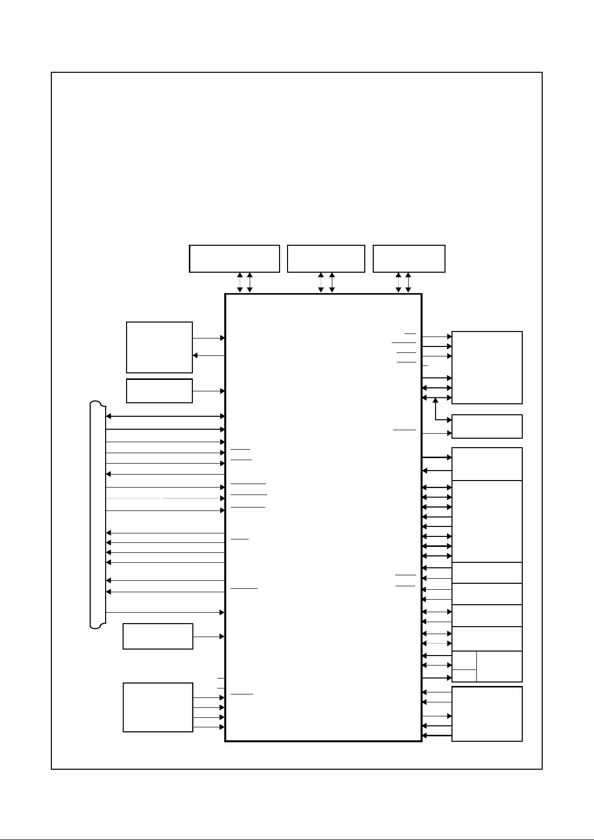
See Figure 1-1 for a system example in IRE environment.
In this environment, the ENV0 and ENV1 strap pins do not
need any external pull-up resistors.
or
Clock
External
Memory
PC87570
Host System Bus (ISA Compatible)
32KX1/32KCLKIN
32KX2
HMR
HA18-0
HD7-0
HIOR
HIOW
IRQ1
IRQ11
IRQ12
RD
WR1-0
SEL0
A18-16, A15-0
D15-8
AD7-0
DA3-0
PA6-0
PB7-0
PC7-0
PD7-0
HIOCHRDY
RTC
Battery
V
BAT
IRQ8
PSCLK1
PSDAT1
Crystal
32.768 KHz
External Keyboard
Internal
Keyboard
KBSOUT15-0
KBSIN7-0
SRAM or
Flash
ENV0
GA20
AVCC
AGND
VCC
GND
Power
Supply
SCL
D7-0
HMEMRD
HMEMWR
PSCLK2
PSDAT2
PSCLK3
PSDAT3
PG4-0
PE1-0
PF7-0
PH5-0
HMEMCS
HAEN
EXINT0,10,11,15
PFAIL
RING
SHBM
HRMS
Configuration
Inputs
I/O
Expansion
TA
HDEN
TRIS
HPWRON
PC0
External Mouse
Auxiliary PS/2
Interface
Interface
Interface
HRSTO
SELIO
(Matrix)
SDA
TB
SWIN
Analog
Reset
Control
(power-up reset)
GPIO
Interrupt
ACCESS.bus
System
Timers
ENV1
NC
NC
Figure 1-1. IRE Environment
SEL1
NC
(Application)
V
REF
ADC
DAC
Page 17
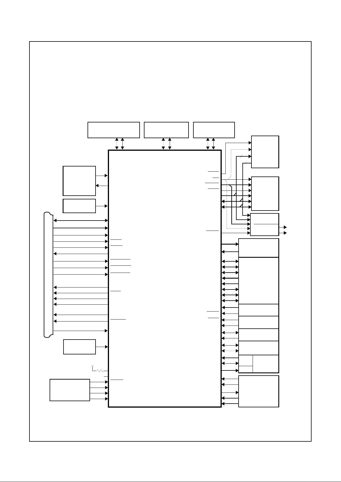
Introduction
OPERATING ENVIRONMENTS
17
www.national.com
1.3.2 IRD Environment
IRD environment is used mostly for prototypes and low-volume manufacturing. In this environment, the on-chip Base
Memory (containing the up to 2 KByte boot code), is replaced by up to 64 Kbytes of off-chip memory, called offchip Base Memory, which may be ROM or Flash memory.
You can control the number of wait states used to access the
Base Memory to allow interfacing with devices that have a
wide range of access times. Configure this number according
to the operation frequency and voltage, and the device access time. Since the time required to access off-chip Base
Memory devices affects the performance of the CR16A core,
use the same number of wait states in all environments to
maintain cycle-by-cycle compatibility.
In this environment, the pins of ports PF and PG are allocated for the interface to the Base Memory. The system may
restore these ports using the I/O Expansion protocol and
off-chip logic, while maintaining cycle-by-cycle and binary
compatibility with the IRE environment. All features of IRE
environment can be implemented either directly or by using
additional external logic.
Figure 1-2 illustrates a system in IRD environment.
or
Clock
External
Memory
PC87570
Host System Bus (ISA Compatible)
32KX1/32KCLKIN
32KX2
HMR
HA18-0
HD7-0
HIOR
HIOW
IRQ1
IRQ11
IRQ12
RD
WR1-0
SEL0
A18-16, A15-0
D15-8
AD7-0
DA3-0
PA6-0
PB7-0
PC7-0
PD7-0
HIOCHRDY
RTC
Battery
V
BAT
IRQ8
PSCLK1
PSDAT1
Crystal
32.768 KHz
External Keyboard
Internal
Keyboard
KBSOUT15-0
KBSIN7-0
SRAM or
Flash
ENV0
GA20
AVCC
AGND
VCC
GND
Power
Supply
SCL
D7-0
HMEMRD
HMEMWR
PSCLK2
PSDAT2
PSCLK3
PSDAT3
PG4-0
PE1-0
PF7-0
PH5-0
HMEMCS
HAEN
EXINT0,10,11,15
PFAIL
RING
SHBM
HRMS
Configuration
Inputs
I/O
Expansion
TA
HDEN
TRIS
HPWRON
PC0
External Mouse
Auxiliary PS/2
Interface
Interface
Interface
HRSTO
SELIO
(Matrix)
SDA
TB
SWIN
Analog
Reset
Control
(power-up reset)
GPIO
Interrupt
ACCESS.bus
System
Timers
ENV1
NC
Figure 1-2. IRD Environment
SEL1
(Application)
V
REF
ADC
DAC
Off-chip
Base
(Boot code
ROM)
Memory
16
16
*
Restored
Ports
*
Optional 8/16 data bus
V
CC
R
1
PF
PG
Page 18
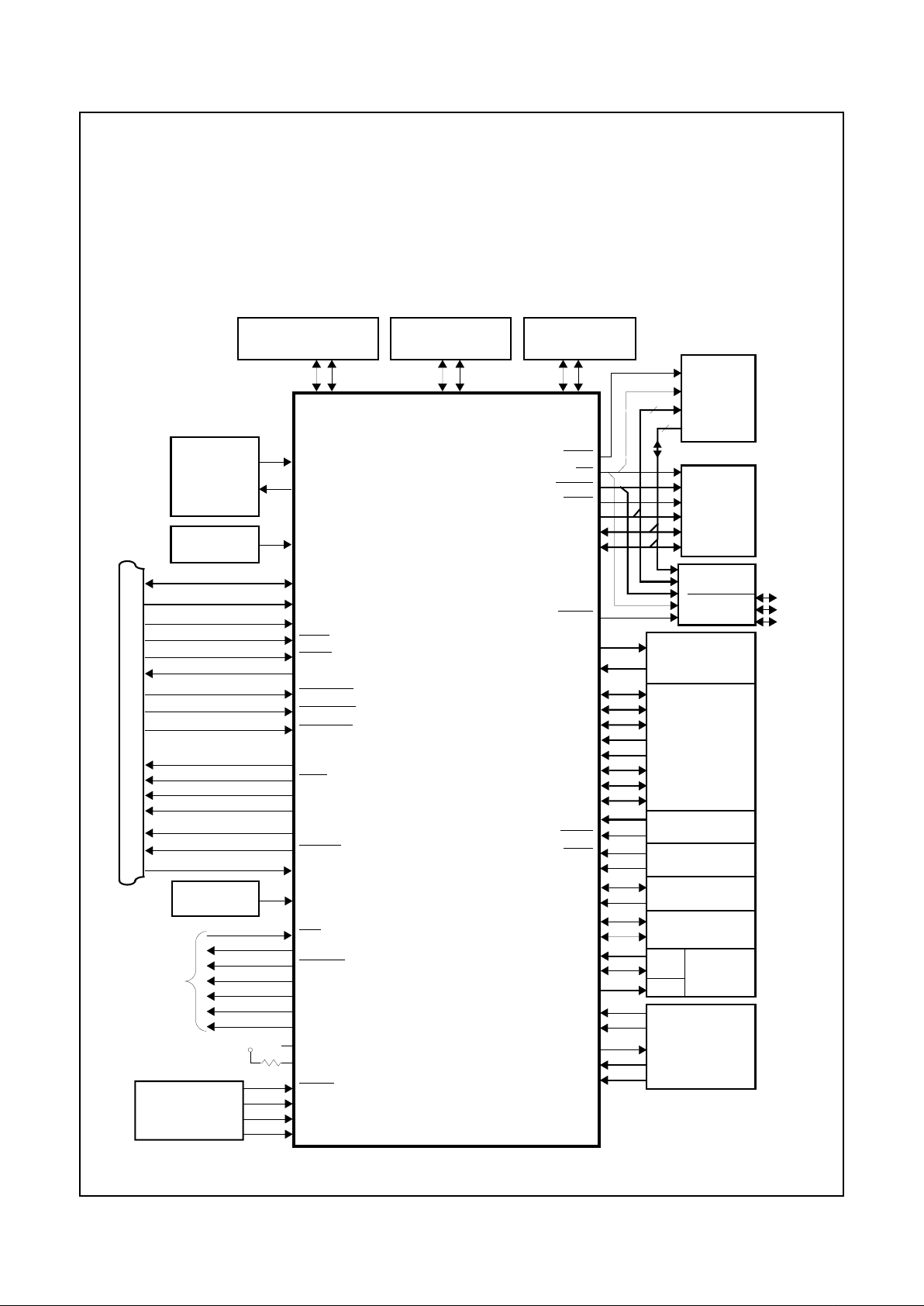
Introduction
18
OPERATING ENVIRONMENTS
www.national.com
1.3.3 DEV Environment
DEV environment is most commonly used to develop software on Application Development Boards (ADBs) and InSystem Emulators (ISEs). In this environment, the development tools can load code and data of up to 64 Kbytes to offchip RAM. This can replace the Base Memory used in
IRE/IRD environment (on-chip/off-chip boot-code). The development tool can also load code and data of up to 56
Kbytes to off-chip RAM (application).
In this environment, the pins of ports PF, PG and PH are allocated for the interface to the Base Memory, for ISE interrupt and for CR16A core status indication. The system may
re-gain these ports using the I/O Expansion protocol and
off-chip logic, while maintaining cycle-by-cycle and binary
compatibility with the IRE environment. Using the same software, this environment is binary and cycle-by-cycle compatible with IRD and IRE environments. All features of IRE
environment can be implemented either directly or by using
additional external logic. Figure 1-3 shows a system in DEV
environment.
or
Clock
External
Memory
PC87570
Host System Bus (ISA Compatible)
32KX1/32KCLKIN
32KX2
HMR
HA18-0
HD7-0
HIOR
HIOW
IRQ1
IRQ11
IRQ12
RD
WR1-0
SEL0
A18-16, A15-0
D15-8
AD7-0
DA3-0
PA6-0
PB7-0
PC7-0
PD7-0
HIOCHRDY
RTC
Battery
V
BAT
IRQ8
PSCLK1
PSDAT1
Crystal
32.768 KHz
External Keyboard
Internal
Keyboard
KBSOUT15-0
KBSIN7-0
SRAM or
Flash
ENV0
GA20
AVCC
AGND
VCC
GND
Power
Supply
SCL
D7-0
HMEMRD
HMEMWR
PSCLK2
PSDAT2
PSCLK3
PSDAT3
PG4-0
PE1-0
PF7-0
PH5-0
HMEMCS
HAEN
EXINT0,10,11,15
PFAIL
RING
SHBM
HRMS
Configuration
Inputs
I/O
Expansion
TA
HDEN
TRIS
HPWRON
PC0
External Mouse
Auxiliary PS/2
Interface
Interface
Interface
HRSTO
SELIO
(Matrix)
SDA
TB
SWIN
Analog
Reset
Control
(power-up reset)
GPIO
Interrupt
ACCESS.bus
System
Timers
ENV1
NC
Figure 1-3. DEV Environment
SEL1
(Application)
V
REF
ADC
DAC
Off-chip
Base
(Boot code
SRAM)
Memory
16
16
*
Restored
Ports
*
Optional 8/16 data bus
V
CC
R
1
PF
PG
PH
CLK
ISE
BST2-0
PFS
PLI
Development
Support
BE1,0
CBRD
Page 19

Signal/Pin Connection and Description
19
2.0 Signal/Pin Connection and Description
www.national.com
2.0 Signal/Pin Connection and Description
2.1 CONNECTION DIAGRAMS
80
75
70
65
60
55
50
1 5 10 15 20 25 30
859095100
4035
PC87570
105110115120
45
41
81
121
125
130
135
140
145
150
155
160
HD0
HD1
GND
HD2
HD3
HD4
HD5
HD6
HD7
GND
V
BAT
KBSIN7
KBSIN2
KBSIN1
KBSIN3
PH1/BST1/ENV1
PG3/
SEL1
V
CC
SEL0/HRMS
PH2/BST2/TRIS
HIOCHRDY
DA1
GND
PH4/PLI
PH3/PFS
PH5/
ISE
PD6/AD6
PH0/BST0/ENV0
PG2/CLK
DA0
DA3
DA2
PB5(GA20)
AGND
HA9
A6A5A4A3A2
PA2/HMEMWR
HMR
HPWRON
HA0
PB7/SWIN
A8
IRQ12
IRQ11
A14/BE1
A10
A11A7A9
PA6/A17
A13/BE0
PE0/HA18
HRSTO(PB6)
KBSOUT0
HA10
HA11
HA12
HA13
HA14
HA15
PA3/HA16
PA4/HA17
PSDAT1
PC7/PSDAT3
PB0/RING
KBSIN5
KBSIN6
PC6/PSCLK3
PC5/EXINT15
RD/HDEN
PG0/
SELIO
WR0
PG4/WR1
A1
A0
KBSOUT1
KBSOUT2
KBSOUT3
KBSOUT4
PC4/EXINT11
PD7/AD7
PF3/D11
PF4/D12
PF1/D9
PF2/D10
PF6/D14
PF5/D13
PF7/D15
PF0/D8
KBSOUT5
KBSIN4
KBSIN0
KBSOUT15
KBSOUT6
KBSOUT7
KBSOUT8
KBSOUT9
KBSOUT14
KBSOUT13
KBSOUT12
KBSOUT11
HA1
HA2
HA3
HA4
HA5
HA6
HA7
GND
V
CC
PSDAT2
PSCLK1
PC3/EXINT0
PC2
PC1
PSCLK2
PC0
A12
32KX2
KBSOUT10
PA5/A16
HIOR
HIOW
IRQ1
PA0/HMEMCS
V
CC
GND
PA1/HMEMRD
IRQ8
PG1/A15/CBRD
PE1/A18/SHBM
D0
D1
D2
D3
D4
D5
D6
D7
AV
CC
PD5/AD5
PD4/AD4
PD3/AD3
PD2/AD2
PD1/AD1
PD0/AD0
V
REF
PFAIL
PB3/TA
PB2/SDA
PB1/SCL
PB4/TB/EXINT10
HA8
V
CC
160-pin PQFP
32KX1/32CLKIN
160-pin PQFP Package
Order Number PC87570-ICC/VUL
NS Package Number VUL160
HAEN
Page 20

Signal/Pin Connection and Description
20
CONNECTION DIAGRAMS
www.national.com
32KX1/32CLKIN
85
80
75
70
65
60
55
5 101520253035
95100105110
40
PC87570
115120125130
50
90
135
140
145
150
155
160
165
170
175
HD0
HD1
HAEN
GND
HD2
HD3
HD4
HD5
HD6
HD7
GND
V
BAT
KBSIN7
KBSIN2
KBSIN1
KBSIN3
PH1/BST1/ENV1
PG3/SEL1
V
CC
SEL0/HRMS
PH2/BST2/TRIS
HIOCHRDY
DA1
GND
PH4/PLI
PH3/PFS
PH5/
ISE
PD6/AD6
PH0/BST0/ENV0
PG2/CLK
DA0
DA3
DA2
PB5(GA20)
AGND
HA9
A6A5A4A3A2
PA2/HMEMWR
HMR
HPWRON
HA0
PB7/SWIN
A8
IRQ12
IRQ11
A14/BE1
A10
A11A7A9
PA6/A17
A13/BE0
PE0/HA18
HRSTO(PB6)
KBSOUT0
HA10
HA11
HA12
HA13
HA14
HA15
PA3/HA16
PA4/HA17
PSDAT1
PC7/PSDAT3
PB0/RING
KBSIN5
KBSIN6
PC6/PSCLK3
PC5/EXINT15
RD/HDEN
PG0/SELIO
WR0
PG4/
WR1
A1
A0
KBSOUT1
KBSOUT2
KBSOUT3
KBSOUT4
PC4/EXINT11
PD7/AD7
PF3/D11
PF4/D12
PF1/D9
PF2/D10
PF6/D14
PF5/D13
PF7/D15
PF0/D8
KBSOUT5
KBSIN4
KBSIN0
KBSOUT15
KBSOUT6
KBSOUT7
KBSOUT8
KBSOUT9
KBSOUT14
KBSOUT13
KBSOUT12
KBSOUT11
HA1
HA2
HA3
HA4
HA5
HA6
HA7
GND
V
CC
PSDAT2
PSCLK1
PC3/EXINT0
PC2
PC1
PSCLK2
PC0
A12
32KX2
KBSOUT10
PA5/A16
HIOR
HIOW
IRQ1
PA0/
HMEMCS
V
CC
GND
PA1/HMEMRD
IRQ8
PG1/A15/CBRD
PE1/A18/SHBM
D0
D1
D2
D3
D4
D5
D6
D7
AV
CC
PD5/AD5
PD4/AD4
PD3/AD3
PD2/AD2
PD1/AD1
PD0/AD0
V
REF
PFAIL
PB3/TA
PB2/SDA
PB1/SCL
PB4/TB/EXINT10
HA8
V
CC
176-pin TQFP
1
176-pin Thin Quad Flatpack (TQFP)
Order Number PC87570-ICC/VPC
NS Package Number VPC176
NC
NC
NC
NC
NC
NC
NC
NC
NC
NC
NC
NC
NC
NC
NC
NC
45
Page 21

Signal/Pin Connection and Description
SIGNAL/PIN DESCRIPTIONS
21
www.national.com
2.2 SIGNAL/PIN DESCRIPTIONS
Refer to Table 2-2 for an alphabetical listing of all PC87570 signals and pins, as well as brief descriptions. The following
abbreviations are used in the Type column in this table.
Table 2-1. Type Symbols
Table 2-2. PC87570 Signals
Symbol Description DC Characteristics
TTL Input, TTL compatible See Table 19-7 on page 135.
CMOSS Input, CMOS with Schmidt Trigger See Table 19-7 on page 135.
STRAP Input with Schmidt characteristics and an internal
pull-down resistor, typically used for strap signals
See Table 19-7 on page 135.
CM Output, CMOS buffer See Table 19-7 on page 135.
CMHD1 Output, CMOS buffer with high drive type 1 See Table 19-7 on page 135.
CMHD2 Output, CMOS buffer with high drive type 2 See Table 19-7 on page 135.
OD Output, Open-Drain See Table 19-7 on page 135.
OD2 Output, Open-Drain with high drive type 2 See Table 19-7 on page 135.
PU Weak pull-up capability (on input or output pin) See Table 19-7 on page 135.
OSCIN Oscillator input [not characterized]
OSCOUT Oscillator output [not characterized]
ANIN Analog input signal See Table 19-5 on page 134.
ANOUT Analog output signal See Table 19-6 on page 134.
Signal
Pin Number Buffer Type
Function
160-pin 176-pin Input Output
32KCLKIN 23 25 TTL - 32.768 KHz Oscillator Clock Input..
32KX1 23 25 OSCIN 32.768 KHz Crystal Interface, input to oscillator.
32KX2 25 27 - OSCOUT 32.768 KHz Crystal Oscillator Interface output
to crystal. See Figure 6-1 on page 65.
A18-0 122-104 136, 135,
130-114
- CM Address A18 through A0. CR16A address to
external memory. A16-A17 should not be pulled
up during power-up since include special test
features.
AD7-0 84, 83,
80-75
95, 94,
86-81
ANIN - Analog Inputs of the A/D converter
AGND 82 92 N/A N/A Analog Ground, for ADC and DAC.
AV
CC
81 91 N/A N/A Analog 5V or 3.3V power supply.
BE1,0 118, 117 128, 127 - CM Byte Enable bits 1 and 0 on monitor bus cycles.
BST2-0 92-94 102-104 - CM Bus Status bits 2-0 on monitor bus cycles.
When in DEV environment, these pins allows
monitoring of the external bus cycles. When
BCFG.OBR is also set, the internal bus cycles
are also visible outside. See also Table 2-5 on
page 27.
CBRD 119 129 - CM Core Bus Read Status on monitor bus cycles.
Available in all modes. See Table 2-5 on
page 27.
Page 22

Signal/Pin Connection and Description
22
SIGNAL/PIN DESCRIPTIONS
www.national.com
CLK 97 107 - CM PC87570 internal clock (On-chip Clock Multi-
plier output). Available in all environments. For
IRE environment, set MCFG.CLKOE=1. See
Table 2-5 on page 27.
D15-0 138-123 152-137 TTL CM CR16A Memory Data bus bits 15 through 0.
DA3-0 88-85 98-95 - ANOUT Digital to Analog Converter Output.
ENV1,0 93, 94 103, 104 STRAP - Environment select strap pins.These pins define
if the device environment, IRE, IRD or DEV.
They are sampled on power-up reset. See Sec-
tion 2.4 on page 26.
EXINT0
EXINT10
EXINT11
EXINT15
58
69
59
62
64
75
65
68
TTL - External Interrupt Inputs 0, 10, 11, 15. Interr upt
signals for general purpose use. These interrupt
signals are asynchronous. See Table 9-2 on
page 82.
GA20 70 76 - CM Gate A20 output. See Section 5.11.6 on page
54.
GND 22, 24,
60, 99,
146
24, 26,
66, 109,
160
N/A N/A Ground for both on-chip logic, output drivers
and back-up battery circuit. See Figure 19-1 on
page 132 for details on connections with
AGND. See also Figure 16-4 on page 125 and
Figure 17-2 on page 129.
HA18-0 10-1,
160-152
12-3,
174-166
TTL - Host Address lines inputs to address registers
in the KBC, PM, RTC/APC and the configura-
tion registers. See Section 5.5.2 on page 50
and Section 5.4.3 on page 50. See also
“HPWRON” pin description below.
HAEN 11 13 TTL - Host Address Enable should be low during
HIORD and HIOWR bus transactions, otherwise
the bus transaction is ignored. Refer to Section
19.5.4 on page 150.
HD7-0 20-13 22-15 TTL CMHD2 Host Data. Bi-directional data bus used to inter-
face the PC87570 to the peripheral data bus of
the host. Refer to Section 19.5.4 on page 150.
HDEN 101 111 STRAP - Host Device Enable, strap pin.
When pulled high during power-up reset, con-
figures the Host device (host interface and
RTC) to be enabled as default after each reset.
When low during power-up reset, the mother-
board PnP protocol must be used to enable the
host access to these devices after each reset.
See Section 2.4.2 on page 26 and Section
5.11.5 on page 54.
HIOCHRDY 12 14 - OD2 Host I/O Channel Ready. An open drain output
that enables extending the host access. This is
used for handling the dual ported access to the
CMOS RAM and to share memory with the
host. See “HRMS” and “HPWRON” pins
description below.
HIOR 144 158 TTL - Host I/O Read. Active-low input that signals an
I/O data read by the host processor.
Signal
Pin Number Buffer Type
Function
160-pin 176-pin Input Output
Page 23

Signal/Pin Connection and Description
SIGNAL/PIN DESCRIPTIONS
23
www.national.com
HIOW 145 159 TTL - Host I/O Write. Active-low input that signals an
I/O data write by the host processor.
HMEMCS 143 157 TTL - Host BIOS Memory Chip Select. This signal is
in use when the shared memory configuration is
enabled (
SHBM=0). See pin “SHBM” below .
See also Table 2-5 on page 27.
HMEMRD 148 162 TTL - Host Memory Read. Active-low input that sig-
nals a memory data read by the host processor.
This signal is in use when the shared memory
configuration is enabled (
SHBM=0). See pin
“SHBM” below . See also Table 2-5 on page 27.
HMEMWR 149 163 TTL - Host Memory Write. Active-low input that sig-
nals a memory data write by the host processor.
This signal is in use when the shared memory
configuration is enabled (
SHBM=0). See pin
“SHBM” below . See also Table 2-5 on page 27.
For AC parameters, refer to Section 19.5.4 on
page 150.
HMR 150 164 CMOSS - Master Reset. A rising edge that resets the
PC87570. See details at Section 2.3.4 on page
26.
HPWRON 151 165 CMOSS - Host Power On. Indicates that the host power
supply is on, and the host bus interface signals
are valid. While HPWRON is low, the host
inputs are ignored, and all outputs are either
floating or driven low. See Section 5.11.2 on
page 53.
HRMS 95 105 STRAP - Host Reset Mode Select, strap pin. When pulled
high during power-up reset, enables sending
reset event to the Host processor when the
shared BIOS is accessed while the PC87570 is
not in Active mode, or the MCFG.SHOFF or
MCFG.SHMEN are 0. When low, the host
access is extended until the PC87570 completes its execution.
HRSTO 71 77 - CM Host Reset Output
IRQ1 142 156 TTL CMHD2
OD2
Interrupt 1. Active-high output to signal a keyboard interrupt. This bit is set when the KBC
port output buffer is full with data to the keyboard driver.
IRQ8 141 155 - OD2 Interrupt 8. Active-low output that Indicates an
RTC interrupt.
IRQ11 140 154 TTL CMHD2
OD2
Interrupt 11. Active-high output that indicates an
output buffer full in the Power Management port
of the Host I/F.
IRQ12 139 153 TTL CMHD2
OD2
Interrupt 12. Active-high output that indicates a
mouse interrupt. This bit is set when the KBC
port output buffer is full with data for the mouse
driver.
ISE 89 99 TTL - ISE Interrupt. Reser ved for use by the develop-
ment system.
Signal
Pin Number Buffer Type
Function
160-pin 176-pin Input Output
Page 24

Signal/Pin Connection and Description
24
SIGNAL/PIN DESCRIPTIONS
www.national.com
KBSIN7-0 27-34 29-36 CMOSS-PU - Internal Keyboard Input scan lines
KBSOUT15-0 35-50 37-42,
47-56
- OD Internal Keyboard Output scan lines
PA6-0 121, 120,
9, 8,
149, 148,
143,
135, 130,
11, 10,
163, 162,
157
TTL-PU CM-PU Port A, bits 0 through 6
PB7-0 72-65 78-71 TTL-PU CM-PU Port B, bits 0 through 7
PC2-0 57-55 63-61 TTL-PU CMHD1-PU Port C, bits 0 through 2 high drive output buff ers
PC7-3 64-62, 59, 58 70-68, 65, 64 TTL-PU CM-PU Port C, bits 3 through 7
PD7-0 84, 83, 80-75 94, 93, 86-81 TTL - Port D, bits 0 through 7, input port only
PE1,0 122, 10 136, 12 TTL-PU CM-PU Port E, bits 0 through 1
PF7-0 138-131 152-145 TTL CM Port F, bits 0 through 7
PFAIL 73 79 CMOSS - Power Fail. Non-maskable interrupt input
detected
PFS 91 101 - CM Pipe Flow Status signal
PG4-0 103, 96,
97, 119,
100
113, 106,
107, 129,
110
TTL CM Port G, bits 0 through 4
PH5-0 89-94 99-104 TTL CM Port H, bits 0 through 5
PLI 90 100 - CM Pipe Long Instruction signal
PSCLK1
1
52 58 TTL-PU
CMHD1-PU
1
PS/2 Channel 1 Clock signal
PSCLK2
1
54 60 TTL-PU
CMHD1-PU
1
PS/2 Channel 2 Clock signal
PSCLK3
1
64 70 TTL-PU
CMHD1-PU
1
PS/2 Channel 3 Clock signal
PSDAT1
1
51 57 TTL-PU
CMHD1-PU
1
PS/2 Channel 1 Data signal
PSDAT2
1
53 59 TTL-PU
CMHD1-PU
1
PS/2 Channel 2 Data signal
PSDAT3
1
63 69 TTL-PU
CMHD1-PU
1
PS/2 Channel 2 Data signal
RD 101 111 - CMHD Read control signal. May be used as Output
Enable.
RING 65 71 CMOSS - Advanced P ower Control Ring detect and wake-
up input
SCL 66 72 CMOSS-PU OD-PU ACCESS.bus Serial Clock signal
SDA 67 73 CMOSS-PU OD-PU ACCESS.bus Serial Data signal
SEL0 95 105 - CM Zone Select 0. Chip-select signal for the Exter-
nal Memory.
SEL1 96 106 - CM Zone Select 1. Used to select the off-chip Base
Memory.
SELIO 100 110 - CM I/O Expansion chip-select signal
SHBM 122 136 STRAP - Shared host BIOS Memory. Enable when 0
SWIN 72 78 STRAP - On switch to the MIWU and ICU
TA 68 74 TTL CM Timer pin A
Signal
Pin Number Buffer Type
Function
160-pin 176-pin Input Output
Page 25

Signal/Pin Connection and Description
SIGNAL/PIN DESCRIPTIONS
25
www.national.com
1. This is a quasi-bidirectional output. It has drive low capability. It is pulsing high for a short period; steady state:
pull high using a weak pull-up. See also Section 12.2.3 on page 90
TB 69 75 TTL - Timer pin B
TRIS 92 102 STRAP - TRI-STATE strap option. When high, during
power-up reset, causes the PC87570 to float all
its output and I/O signals.
V
BAT
26 28 IN
ULR
- Battery supply. This is the 2.4 - 5.5V battery
voltage for the RTC circuitry.
V
CC
21, 61,
98, 147
23, 67,
108, 161
N/A N/A Digital 5V or 3.3V power supply
V
REF
74 80 ANIN ANOUT Reference voltage for the on-chip A/D circuits.
With the internal V
REF
enabled a capacitor is
connected between V
REF
and GND. When the
internal V
REF
is disabled, an External Refer-
ence voltage should be connected to this input.
WR1,0 103, 102 113, 112 - CM Write control for bytes 0 and 1
Signal
Pin Number Buffer Type
Function
160-pin 176-pin Input Output
Page 26

Signal/Pin Connection and Description
26
RESET SOURCES AND TYPES
www.national.com
2.3 RESET SOURCES AND TYPES
2.3.1 Power-Up Reset
The PC87570 includes an internal power-up reset circuit
This circuit generates the power-up reset signal which
During power-up reset, the PC87570 responds as follows:
●
Carries out all the warm reset actions
●
Enables the 32K crystal, if it is disabled
●
Resets the HFCG Register to its default frequency
●
Loads preset values to all register.
●
Puts pins with strap options into TRI-STATE, and enables the internal pull-downs on the strap pins
●
Samples the values of the strap pins.
2.3.2 Warm Reset
During a warm reset, the PC87570 responds as follows:
●
Ter minates instructions being executed
●
Discards results not yet written to memory
●
Traps and eliminates pending interrupts
●
Clears the internal latch for the edge-sensitive external
interrupt
●
Deactivates the external bus control signals WR(0-1),
SEL(0-1), SELIO, RD and BST(0-2)
●
Puts the address A(0-15) and data D(0-15) buses in
TRI-STATE
●
Switches to Active mode
●
Loads preset values into registers
●
Sets the motherboard PnP mechanism to its reset
state.
Certain registers, such as the HFCG and Port PC Registers,
are affected only by power-up and/or WATCHDOG reset.
During warm reset, the strap pins are not sampled and the
configuration determined at power-up is unaffected by subsequent warm resets.
2.3.3 WATCHDOG Reset
During a WATCHDOG reset, the PC87570 performs the
power-up reset actions with one exception: it does not sample the value of the strap pins. Instead, it maintains the configuration determined by the strap pins at power-up reset.
2.3.4 Triggering Reset
The PC87570 is reset by an internal reset signal generated
on the ramp-up of the V
CC
power supply (cold reset). The
chip is also reset on the rising edge of the HMR pin (warm
reset).
Power-Up Reset The PC87570 performs a power-up reset
when power is applied to it. This reset is completed t
IRST
after the internal clock has stabilized. See Figure 19-25 on
page 154.
If the RTC clock was disabled before power-up, external devices should wait at least t
32KW
(see before accessing the
PC87570. If HRMS=0, any access by the host processor is
stalled, by de-asserting (0) HIOCHRDY, until after the reset
process is completed and the bus request can be performed.
Warm Reset A rising edge of the HMR input initiates a
warm reset. The rising edge is identified only when power
(V
CC
) is applied to the PC87570 completed the internal
power-up reset cycle. The reset continues for a period of
about 16 clock cycles after the HMR rising edge. See details
at Figure 19-26 on page 154.
The PC87570 can operate when HMR is still active (high).
In this case, the host bus I/F is inactive.
Note: In all PC87570 revisions, before C3, the HMR (formerly HMR) input pin is ignored when HPWRON is 0, disabling reset execution.
WATCHDOG Reset
The PC87570 generates a WATCHDOG reset on request
from the TWD (WATCHDOG signal is asserted). The reset
period is identical to the power-up reset period.
2.4 STRAP PINS
During power-up reset, the ENV(0-1), TRIS, HRMS, HDEN
and
SHBM strap input signals are sampled. Internal pulldown resistors set these signals to 0. You can use an external 10 KΩ resistor connected to V
CC
to set them to 1.
2.4.1 Setting the Environment
ENV0 and ENV1 determine the operating environment. Table 2-3 shows the settings allowed. Pulling both ENV0 and
ENV1 to 1 at the same time produces unpredictable results.
Table 2-3. Environment Pin Settings
Figures 1-1 on page 16, 1-2 on page 17, and 1-3 on page
18 demonstrate how to use the ENV(0-1) signals to configure the PC87570 for IRE, IRD, and Dev environment, respectively.
2.4.2 Other Strap Pin Settings
Table 2-4 provides brief descriptions of other strap inputs.
For details on
SHBM, HRMS, HDEN and TRIS, see sections 5.2 on page 49, 5.11.4 on page 53, 5.11.5 on page 54
and 18.2 on page 130, respectively.
Table 2-4. Other Strap Pin Settings
Environment ENV0 ENV1
IRE 0 0
IRD 0 1
Dev 1 0
Strap
Pin
Internal Pull-Down (0) External Pull-Up (1)
SHBM Enables shared memory
with host BIOS
Disables shared
memory with host BIOS
HRMS Extends host access
until the PC87570
completes its execution
Enables a reset event to
be sent to the host
when the shared BIOS
is accessed while the
PC87570 is not in
Active mode, or SHOFF
or SHMEM bit is cleared
in MCFG Register
Page 27
Signal/Pin Connection and Description
ALTERNATE FUNCTIONS
27
www.national.com
2.4.3 System Load on Strap Pins
The loads connected to the strap pins should prevent the
voltage on them from dropping below V
STRh
when the pins
should be high (1), or rising above V
STRl
when they should
be low (0). See Table 19-7 on page 135.
If the load caused by the system on the strap pins exceeds
10 µA when V
CC
= 5.0V or 5 µA when VCC= 3.3V, use either an external pull-up resistor or a smaller pull-down resistor to keep the pin at 1 or 0, respectively.
2.4.4 Strap Inputs During Idle Mode
When the PC87570 is in Idle mode and shared memory with
host BIOS is enabled, the A(16-18) signals are forced to the
value sampled on the strap input that shares the pin. This is
done to reduce leakage currents on external resistors connected to that pin.
Note: A(16-17) are reserved strap inputs that should not
be pulled to 1.
2.4.5 Strap Pin Status Register (STRPST)
The STRPST Register is a byte-wide, read-only register. It
enables the software to read the value set to strap pins during power-up reset. STRPST bits provide the value of their
respective strap input. See Table 2-5 for bit details.
2.5 ALTERNATE FUNCTIONS
The PC87570 uses the GPIO port pins to multiplex functions and thereby maximize the device’s flexibility, as
shown in Table 2-5. You select alternate pin functions
through the configuration registers and strap options, as follows:
●
The SHBM strap pin (see Table 2-4) controls the PA
pins. When
SHBM = 1, the pins function as GPIO port
signals. When
SHBM=0, they function as described in
Section 5.2.1 on page 49.
●
The ports’ Alternate Function Control Register controls
the PB, PC, PD and PE pins. Each of the ports’ pins
may be used as a GPIO port or in its alternate function.
●
The environment setting and MCFG bits control port
PF and PG pins.
●
The environment setting controls port PH pins. When
in Dev environment, the pins perform their alternate
functions. In IRE or IRD environments, they function
as GPIO ports.
When a pin is used as GPIO and not in its alternate function,
disable the alternate function in the module’s register to prevent wired effects.
Table 2-5 lists the I/O pins and their alternate functions.
When you use a pin as GPIO, you should disable the alternate function in the module register to prevent wired effects.
Table 2-5. Alternate Function Mapping
HDEN Disables host interface;
must be enabled using
the motherboard PnP
protocol after each reset
Enables host interface
to its default settings
(legacy address of KBC,
RTC and PMC)
TRIS Normal operation Causes PC87570 to
float all its output and
I/O signals for ISE use
Strap
Pin
Internal Pull-Down (0) External Pull-Up (1)
7 3 2 1 0
Reserved HDEN HRMS SHBM
Pin Name
Port Signal
Alternate
Function
Select
(Alternate Function)
Name Type
PA0/
HMEMCS PA0
I/O
HMEMCS
SHBM=0
PA1/
HMEMRD PA1 HMEMRD
PA2/
HMEMWR PA2 HMEMWR
PA3/HA16 PA3 HA16
PA4/HA17 PA4 HA17
PA5/A16 PA5 A16
PA6/A17 PA6 A17
Page 28

Signal/Pin Connection and Description
28
ALTERNATE FUNCTIONS
www.national.com
PB0/RING PB0
I/O
RING PBALT.0
PB1/SCL PB1 SCL PBALT.1
PB2/SDA PB2 SDA PBALT.2
PB3/TA PB3 TA PBALT.3
PB4/TB/EXINT10 PB4 TB/EXINT10 PBALT.4
PB5/GA20 PB5
1
GA20 0 always
PB6/
HRSTO PB6
2
HRSTO 1 always
PB7/SWIN PB7 SWIN PBALT.7
PC0 PC0
I/O
- PCALT.0
PC1 PC1 - PCALT.1
PC2 PC2 - PCALT.2
PC3/EXINT0 PC3 EXINT0 PCALT.3
PC4/EXINT11 PC4 EXINT11 PCALT.4
PC5/EXINT15 PC5 EXINT15 PCALT.5
PC6/PSCLK3 PC6 PSCLK3 PCALT.6
PC7/PSDAT3 PC7 PSDAT3 PCALT.7
PD0/AD0 PD0
Input
AD0 PDALT.0
PD1/AD1 PD1 AD1 PDALT.1
PD2/AD2 PD2 AD2 PDALT.2
PD3/AD3 PD3 AD3 PDALT.3
PD4/AD4 PD4 AD4 PDALT.4
PD5/AD5 PD5 AD5 PDALT.5
PD6/AD6 PD6 AD6 PDALT.6
PD7/AD7 PD7 AD7 PDALT.7
PE0/HA18 PE0
I/O
HA18 PEALT.0
PE1/A18 PE1 A18 PEALT.1
PF0/D8 PF0
I/O
D8
Dev or IRD Env;
IRE Env when
MCFG.EXM16=1
PF1/D9 PF1 D9
PF2/D10 PF2 D10
PF3/D11 PF3 D11
PF4/D12 PF4 D12
PF5/D13 PF5 D13
PF6/D14 PF6 D14
PF7/D15 PF7 D15
Pin Name
Port Signal
Alternate
Function
Select
(Alternate Function)
Name Type
Page 29
Signal/Pin Connection and Description
SYSTEM CONFIGURATION REGISTERS
29
www.national.com
1. PB5 is initialized upon reset as an output port with data set to 1. This allows the
PC87570 firmware to use it as GA20.
2. PB6 is always configured as output and with its alternate function enabled. See
Section 5.11.4 on page 53.
2.6 SYSTEM CONFIGURATION REGISTERS
2.6.1 Module Configuration Register (MCFG)
The MCFG Register is a read/write, byte-wide register. It is
used for global system configuration and setup.
Write operations to the MCFG Register should write zeros
to all reserved bits. Upon reset, non-reserved bits of MCFG
are cleared to 0. MCFG can be written in Active mode only.
Its contents is preserved in Idle mode.
In IRE environment, all fields of MCFG should be used to
designate associated pins as GPIO ports or for their alternate functions. In IRD and Dev environments, the pins are
always allocated for IRD or Dev use. The I/O ports functionality can be implemented using off-chip logic.
To guarantee binary and cycle-by-cycle compatibility
among the different environments, define the MCFG fields
as required for IRE even when in IRD or Dev environments,
and use the I/O Expansion protocol to build an off-chip implementation of the I/O ports when they are used by the application.
ADBs or ISE systems may use the MCFG Shadow (MCFGSH) Register to select the functionality of the signal that
reaches the user’s application.
Bit 0 - Base Memory Shadow Off (SHOFF)
While cleared, the Base Memory can be accessed starting from address 10000h and the External Memory cannot be accessed. When set, this signal turns off the
Base Memory shadow (i.e., the copy that starts at address 00000h) and enables access to the External
Memory. Once SHOFF is set, the firmware should not
clear it.
Bit 1 - Shared Memory Access Enable (SHMEM)
The host processor is enabled to access the shared
memory only when SHMEM and SHOFF are set. Additional conditions to the host access are described in
Sections 2.7 on page 30 and 5.2 on page 49. When
SHMEM is cleared the host access to the shared memory is disabled. Once SHMEN is set, the firmware
should not clear it.
Bit 2 - External Memory 16-Bit (EXM16)
While cleared, it defines the External Memory as 8 bits
wide. When set it enables the use of a 16-bit wide External Memory. The bus width as indicated in this register
and the bus width as defined in zone0 of the BIU
(SZCFG0) should be the same.
When a 16-bit wide External Memory is used, ports
PF0-7 and PG4 serve as part of the memory interface.
PG0/
SELIO PG0
I/O
SELIO Dev or IRD Env;
IRE Env when
MCFG.EXIOE=1
PG1/A15/CBRD PG1 A15/CBRD Dev or IRD Env;
IRE Env when
MCFG.A15E=1
PG2/CLK PG2 CLK Dev or IRD Env;
IRE Env when
MCFG.CLKOE=1
PG3/
SEL1 PG3 SEL1 Dev or IRD Env;
IRE Env when
MCFG.EXM16=1
PG4/
WR1 PG4 WR1
PH0/BST0/ENV0 PH0
I/O
BST0
Dev Env
PH1/BST1/ENV1 PH1 BST1
PH2/BST2 PH2 BST2
PH3/PFS PH3 PFS
PH4/PLI PH4 PLI
PH5/
ISE PH5 ISE
Pin Name
Port Signal
Alternate
Function
Select
(Alternate Function)
Name Type
7 6 5 4 3 2 1 0
Res CLKOE EXIOE A15E EXM16 SHMEM SHOFF
Page 30

Signal/Pin Connection and Description
30
SHARED MEMORY CONFIGURATION
www.national.com
Bit 3 - Address A15 Enable (A15E)
When cleared (0), the PG1/A15 pin is used as a PG1
GPIO port. When it is set (1), the pin is used to output
address line A15. This allows interface to up to 56 Kbyte
of External Memory. It is set when shared BIOS memory
mode is detected.
Bit 4 - Expansion I/O Enable (EXIOE)
When cleared (0), the PG0/
SELIO pin is used as a
GPIO port signal (PG0). When set (1), the pin is used to
output
SELIO signal. SELIO allows the use of the I/O
Expansion protocol to implement I/O ports off-chip, in
addition to the I/O ports implemented on-chip.
BIt 5 - Clock Output Enable (CLKOE)
When cleared (0), the PG2/CLK pin is used as a general-purpose port signal (PG2). When set (1), the port outputs the clock signal.
Bit 6 - Test Hook Set Flag (TEST)
This bit is set only when the test hook is enabled. The
Base Memory should jump to the test hook routine when
this bit is identified as high. Any device used in the IRE
environment must hold this code. This is a read only bit.
When modifying the MCFG Register, always write 0 to
this bit.
2.6.2 PAGE Register
The PAGE Register is a read/write, byte wide register.
When shared memory is used, this register defines the most
significant bits of the address used when the CR16A core
access the External Memory (zone 0). This defines which
part of the shared memory the PC87570 firmware uses.
During host processor access to the shared memory, the
address lines are taken from the host address bus and not
from the Page Register.
See “External Memory Mapping into Shared BIOS Memory”
on page 32 for an explanation of how the bits below are
used to map the External Memory.
2.7 SHARED MEMORY CONFIGURATION
The PC87570 can share the use of the same memory device with the host processor. Either Flash EPROM or ROM
devices may be used. The memory can be up to 512 KByte.
The PC87570 is mapped into a block of 56 KByte in the
memory device. It may use all the block or part of it.
The host can access any of the bytes in the Flash device.
The BIOS program may be stored at any location not used
by the PC87570 firmware, even within the block assigned to
it.
To share the BIOS memory, hold the
SHBM strap input low
during power-up reset. The firmware should perform the following initialization steps after reset:
1. Set MCFG.A15E to 1 and MCFG.EXM16 according to
the value of PH[3].
2. Set MCFG.SHOFF to enable access to the External
Memory.
3. Load the Page Register with the firmware’s base address of the Shared BIOS block that needs to be accessed.
4. Configure the memory (zone0) access parameters (i.e.,
bus width, write cycle type, number of wait and hold cycles) using the Page and SZCFG0 Registers. The memory device may be either 8 or 16 bits wide; the host
interface is 8-bits wide and the PC87570 takes care of
the bus width translation.
5. If the memory device is 512 KByte (i.e., above 256
KByte), set the PEALT.0 and PEALT.1 bits, configuring
PE0 and PE1 to be used in their alternate functions.
HA18 is used as a BIOS page select.
The External Memory may be read or written by the core,
as necessary, during steps 3 through 5, but the shared
memory cannot be accessed by the host processor.
6. Set MCFG.SHMEN only after the above configurations
are completed.
Figure 2-1 describes the hardware scheme used when a
512K Byte, 8-bit wide, Flash memory is connected to the
PC87570 in the shared BIOS memory configuration.
See Section 5.2 on page 49 for more details about the
shared memory interface and the bus protocols in use.
2.8 MEMORY MAP
The memory and I/O devices are directly mapped into the
256-Kbyte address space of the CR16A. The CR16A allows
the first 128 Kbytes (00000h-1FFFFh) of its address space
to include both code and data.
The boot section code and constant data of a PC87570based system is stored in the Base Memory. This memory is:
●
On-chip ROM in IRE environment
●
Off-chip memories (ROM, Flash or SRAM memory) in
IRD or Dev environment.
Most of the code and constant data of the PC87570 is
stored in the External Memory. This memory can be either
a ROM, Flash or RAM device interfaced directly with the
PC87570. A power-up configuration pin allows memory
sharing with the host processor.
Only byte-wide transactions may access byte-wide registers, and only word-wide transactions may access wordwide registers. Attempts to read a write-only register or write
to a read-only register cause unpredictable results.
Zeros must be written to reserved bits. Reading reserved
bits returns an undefined value. When modifying a register
with reserved bits, the data read from reserved bits can be
written back to it.
Table 2-6 shows how the PC87570’s memory and I/O devices are mapped in the CR16A address space. Appendix
A on page 156 shows the address map of the registers for
the other modules.
Addresses not included in Table 2-6 or in Chapter A on
page 156 are reserved. Attempts to access unlisted addresses produce unpredictable result
s.
7 3 2 1 0
Reserved PAGE18 PAGE17 PAGE16
Page 31

Signal/Pin Connection and Description
MEMORY MAP
31
www.national.com
2.8.1 Accessing Base Memory
Base Memory Configuration
The environment setting controls the use of on-chip Base
Memory (ROM), or off-chip Base Memory. In all cases, the
memory access parameters (i.e., the number of wait and
hold cycles) are as defined for zone1 of the BIU.
On-Chip Base Memory
In IRE environment, on-chip ROM is used as Base Memory,
as shown in Figure 2-2. To maximize on-chip ROM performance, configure the BIU as described in Section 3.6 on
page 46.
Off-Chip Base Memory
In IRD and Dev environments (when on-chip ROM is not
available), the code and constant data are stored in off-chip
Base Memory. This off-chip Base Memory has 64 Kbytes of
address space (10000h - 1FFFFh). The first 56 Kbyte are
also shadowed to address (00000h - 0DFFFh), when
MCFG.SHOFF=0. Off-chip accesses to this memory zone
are indicated by the
SEL1 output.
Figure 2-3 illustrates how off-chip Base Memory is
mapped to the PC87570’s address space.
Table 2-6. PC87570 Memory Map
1. See Section 2.8.1 for details.
2. See Section 2.8.2 for details.
3. When MCFG.A15E = 1; otherwise reserved.
4. See Appendix A on page 156 for details of the implemented registers.
PC87570
CS
A0-18
D0-7
ROMOE
MEMWR
ROMCS
SHBM
A0-18
SEL0
D0-7
A0-18
D0-7
HA0-18
IORD
IOWR
HD0-7
IORD
IOWR
MEMRD
MEMWR
MEMCS
HAEN
AEN
HIOCHRDY
IOCHRDY
Figure 2-1. Sharing PC87570 Program Memory and BIOS Flash Memory
RD
RD
WR
WR0
BIOS
Flash
Memory
Address
Size
(Bytes)
Description
Environment
Shadow On
1
Shadow Off
2
00000h − 007FFh 2K Base Memory External Memory
IRE00800h − 07FFFh 30K
Reserved
08000h − 0DFFFh 24K External Memory
3
00000h − 0DFFFh 56K Base Memory External Memory IRD, Dev
0E000h - 0EFFFh 4K Reserved
All
0F000h − 0F3FFh 1K System RAM
0F400h - 0F8FFh 1280 Reserved
0F900h
-
0F90Ah 11 HBI
0F90Bh - oF97Fh 117 Reserved
0F980h − 0F98Fh 16 BIU Registers
4
0F990h - 0FAFFh 368 Reserved
0FB00h − 0FBFFh 256 I/O Expansion
0FC00h − 0FFFFh 1K
On-chip modules registers
4
10000h − 107FFh 2K Base Memory
IRE
10800h − 1FFFFh 62K Reserved
10000h − 1FFFFh 64K Base Memory IRD, Dev
20000h − 3FFFFh 128K Reserved All
Page 32

Signal/Pin Connection and Description
32
MEMORY MAP
www.national.com
2.8.2 Accessing External Memory
External Memory Configuration is enabled whenever the
Base Memory Shadow is off (MCFG.SHOFF=1). The BIU
Zone 0 Configuration Register (SZCFG0) controls the
memory access parameters.
The interface to the External Memory is executed using the
SEL0, RD,WR0-1, A0-18 and D0-15 signals. Not all the signals are used in every configuration. Table 2-7 summarizes
the MCFG bit settings, and the signals used for the memory
interface in each configuration.
Figure 2-4 shows the External Memory Address Range
mapping to the CR16A core.
External Memory Mapping into Shared BIOS Memory
When the shared BIOS memory is enabled (
SHBM=0), the
External memory address range is mapped into a memory
device with larger address space. This External Memory access is mapped by padding the core’s 16 lower address bits
with fixed values from the Page Register (used as most significant address lines). See Table 2-8 for details on how to
configure various elements for External Memory expansion.
0
56 K
64 K
128 K
256 K
192 K
Address Map
PC87570
2 K
2 K
On-Chip Base Memory
On-Chip Base Memory
MCFG.SHOFF=0
MCFG.SHOFF=1
Figure 2-2. On-Chip Base Memory (Zone 1) Address Range
0
56 K
64 K
128 K
256 K
192 K
Off-Chip Base Memory
Address Map
Off-Chip Base Memory
128 K
PC87570
MCFG.SHOFF=0
MCFG.SHOFF=1
Figure 2-3. Off-Chip Base Memory (Zone 1) Address Range
56 K
Page 33

Signal/Pin Connection and Description
MEMORY MAP
33
www.national.com
Table 2-7. External Memory Configuration Settings
Table 2-8. External Memory Address Expansion Scheme
1. Legend:
X - Alternate function used (I/O port)
Ai - Signal outputs address bit i when the External Memory accessed
Page - Signal outputs the page defined in the Page Register.
2.8.3 Accessing I/O Expansion Space
The I/O expansion protocol permits you to implement I/O
ports in the system, besides those available on-chip, in all
three environments (IRD, IRE and Dev). In IRD and Dev environments, the I/O expansion protocol enables you to implement the functionality of I/O ports PF, PG and PH using
off-chip external logic. Access to these ports is through the
addresses defined in Chapter A on page 156. The I/O expansion space is mapped to the address space FB00FBFFh. You can use the I/O expansion space as follows:
●
Addresses in the range FB00h-FB11h may be used to
restore GPIO ports PF, PG and PH.
●
Address FBFEh is used only in Dev environment by
the MCFGSH Register, and must be written after each
write to the MCFG with the same data written to the
MCFG.
●
Addresses in the range FB30h-FB5Fh are reserved for
development board use.
The protocol accesses the off-chip I/O expansion using I/O
zone of the BIU. The zone select signal (
SELIO), address
lines A0-7 and the
RD and WR0 signals, are used to inter-
face to the off-chip logic.
External
Memory
Configuration
MCFG
SZCFG0.BW
Interface Signals
SHOFF A15E EXM16 Control Data Addr
Disabled 0 X X X X X X
32K x8 1 0 0 0
SEL0,
WR0, RD
D0-7 A0-14
64K x8 1 1 0 0 A0-15
32K x16 1 0 1 1
SEL0,
WR0-1, RD
D0-15 A0-14
64K x16 1 1 1 1 A0-15
SHBM PEALT.1 MCFG.A15E A18
1
A17 A16 A15
10
0XXXX
1 X X X A15
0
0
1
X
Page17 Page16 A15
1 Page18
0
56 K
64 K
128 K
256 K
192 K
Address Map
External Memory Address
PC87570
32 K
MCFG.A15E=0 MCFG.A15E=1
56 K
Figure 2-4. External Memory (Zone 0) Address Range
Page 34

Bus Interface Unit (BIU)
34
3.0 Bus Interface Unit (BIU)
www.national.com
3.0 Bus Interface Unit (BIU)
The BIU directly interfaces with a wide variety of devices, including ROM, SRAM and FLASH memory devices and I/O
devices. It interfaces via address, data and control buses,
without the need for external glue logic.
3.1 FEATURES
●
Three address zones for static devices (SRAM, ROM,
FLASH, I/O)
●
Basic bus cycle: two clock cycles
●
Configurable fast read bus cycles with one-cycle read
duration
●
Wait states: configurable between zero and seven
clock cycles
●
Hold cycles: configurable between zero and three
clock cycles
●
I/O expansion support
●
Configurable burst on read
●
Burst read: one clock cycle
●
Configurable early write or late write
●
Bus width: configurable per zone - 16-bit or 8-bit
3.2 FUNCTIONAL DESCRIPTION
3.2.1 Interfacing
The BIU interfaces between:
●
The internal core bus
●
External static memory
●
Off-chip I/O (memory mapped) devices
●
On-chip ROM.
The BIU performs the following functions:
●
Distinguishes between three static memory zones
●
Selects the relevant configured parameters of the accessed zone (e.g., the number of wait states)
●
Issues the appropriate bus cycle to access the zone.
Each memory zone has a different address range and a set
of parameters which define the access to this zone. The set
of parameters is software configurable.
3.2.2 Static Memory and I/O Support
The BIU accesses static memory devices (ROM, SRAM,
FLASH and I/O devices) using static read and write bus cycles. The BIU extends the bus cycles with wait cycles, if so
configured.
The BIU supports burst read bus cycles, if the accessed
zone is configured as burstable. (A burst-read bus cycle is
an extension of the basic-read bus cycle in which additional
data is accessed. A burst access usually requires only one
clock cycle per additional data item. It may be extended by
up to two clock cycles per additional data item.).
To support both I/O and static memory devices that require
long hold times at the end of the access, the BIU can be
configured to add up to three T
hold
clock cycles at the end
of the bus cycle. In addition to this, the BIU can be configured to insert a T
idle
clock cycle between two consecutive
accesses in different zones.
3.2.3 Byte Accessing
The internal core bus is 16-bit wide and supports byte and
word transactions.
The BIU issues the appropriate bus cycle to access the right
bytes, according to the core bus transaction and the memory
device bus width.
On write cycles of a single byte, the other eight bits of the bus
are floating.
On read cycles of a single byte, the other eight bits of the bus
are ignored. There is no need for external pull-up resistors.
3.3 CLOCK AND BUS CYCLES
There are two types of bus cycles: data transfer and nondata transfer. Data-transfer bus cycles cause transfer of
data from, or to, the memory device. Non-data transfer bus
cycles (described in Section 3.4 on page 44) are used for
observability of internal bus transactions - they do not involve data transfer from, or to, external devices.
There are four types of data transfer bus cycles:
●
Early write
●
Late write
●
Normal read
●
Fast read.
The BIU uses the BCFG.EWR configuration bit to select the
early or late write data transfer bus cycle. It uses the SZCFGn.FRE bit (where “n” refers to zone 0 or 1) to select normal
read or fast read data transfer bus cycles.
The basic late write bus cycle takes two clock cycles. The basic early write bus cycle takes three clock cycles. When the
BIU uses the early write bus cycle, the
RD signal is not required for interfacing with the memory device (with the exception of FLASH). On reset, early write bus cycle is configured.
The basic normal read bus cycle takes two clock cycles.
Fast read bus cycle always takes one clock cycle. On reset,
normal read bus cycle is configured.
Notes:
1. In the descriptions that follow, the “n” in
SELn signal refers to two of the three permitted BIU select signals
(numbered 0 or 1, corresponding to zone 0 or zone 1 respectively). The third signal is labelled
SELIO.
2. For all timing diagrams, the value of BST0-2 depends
upon the type of core bus transaction.
3.3.1 Clock Cycles
Basic Bus Cycle
A basic bus cycle comprises 1 to 3 clock cycles (depending
upon the type of bus cycle). Adding extra wait or hold clock
cycles extends the data transfer bus cycles. Every data
transfer bus cycle has the T1 and T2 clock cycles, with the
exception of the fast read bus cycle that only has one clock
cycle (T1-2).
T
idle
Cycle
Clock cycles which are not used for bus cycles are called
Idle clock cycles (T
idle
). T
idle
cycles are added when the BIU
does not need to generate a bus transaction, or when spe-
Page 35

Bus Interface Unit (BIU)
CLOCK AND BUS CYCLES
35
www.national.com
cifically configured as a pause between two consecutive
transactions. When more than one T
idle
cycle is requested
as a pause, the T
idle
cycles overlap and only one T
idle
cycle
is added.
T
idle
clock cycles can be inserted between two consecutive
accesses in different zones (to allow long hold times or buffer disable times). To do this either program SZCFGn.IPRE
and/or SZCFGn.IPST (or IOCFG.IPST). See Figure 3-7 on
page 40.
T
idle
clock cycles are also added between an early write and
any read bus cycles, and between a late write and fast read
bus cycles. See Figure 3-12 on page 43.
T1 Cycle
Every bus cycle starts with T1. In this clock cycle the address of the selected device (either external or internal) is
set on the address pins. Write bus cycles never drive data
during T1.
T2 Cycle
The read T2 bus cycles always sample the data at the end
of T2.
The write T2 bus cycles always drive data during T2. If no
T
hold
clock cycles follow, the data bus is put in TRI-STATE
after the T2 cycle.
T1-2 Cycle
The fast read T1-2 bus cycle is one-cycle read duration.
At the beginning of the clock cycle, the address of the se-
lected device is set on the address pins and the
SELn and
RD signals are activated. At the end of the clock cycle, the
BIU samples the data.
T3 Cycle
Early write bus cycles always have the T3 clock cycle. All
other bus cycles do not have this clock cycle.
At the beginning of this clock cycle
SELn (or SELIO) deac-
tivates and then
WR(0-1) deactivates. The address and
data remains valid until T3 is completed. If no T
hold
clock cycles follow, the data bus is put in TRI-STATE after the T3
cycle.
The following clock cycles are optional in a data transfer bus
cycle:
●
TIW (Internal Wait)
●
T
hold
●
T2B (T2 burst)
●
TBW (Burst Wait).
TIW Cycle
Extend the basic data transfer bus cycle by adding wait
clock cycles. To do this, either program SZCFGn.WAIT (or
IOCFG.WAIT) with the required additional wait clock cycles.
Wait clock cycles generated due to SZCFGn.WAIT (or IOCFG.WAIT) are named TIW (internal wait). TIW cycles are
added after T1 and followed by T2 cycles. Data is always
driven during wait clock cycles of a write bus cycle.
TBW Cycle
A burst bus cycle can be extended by one wait clock cycle,
named TBW. This is done according to SZCFGn.WBR. The
address is changed in the beginning of TBW. Write bus cycles do not have this clock cycle.
T2B Cycle
Data of read burst bus cycles is sampled at the end of T2B.
If TBW cycle is not configured, the address is changed in
the beginning of T2B. Write bus cycles do not have this
clock cycle.
T
hold
Cycle
Hold cycles are added after T2 or T2B (if there is a burst bus
cycle) or T3 (according to SZCFGn.HOLD or IOCFG.HOLD); the address and data (during a write bus cycle) are always valid during these cycles. The data bus is
put in TRI-STATE after the last T
hold
.
Special T
idle
Cycle
During T
idle
cycles, one of the SEL0-1 signals and the RD
signal may be activated for one clock cycle. This happens
due to special activity on the internal core bus.
To avoid contention on the memory bus, it is guaranteed
that this clock cycle is followed by a sufficient number of
T
idle
cycles before the next T1 cycle is performed.
The number of T
idle
cycles following is at least the number
required by the selected zone as configured in the HOLD
field of the SZCFGn Register.
3.3.2 Control Signals
A read bus cycle consisting of the basic bus cycle plus additional clock cycles (the burst bus cycle) occurs if the bus
is burstable (SZCFGn.BRE is 1), the configured bus width
is 8 bits, and the core attempts to read a word. When the
bus is not burstable (SZCFGn.BRE is 0), the BIU issues two
separate read bus cycles. Write bus cycles are never burstable, and the BIU always issues two separate write bus cycles.
The write bus cycles use byte write qualifiers on
WR0-1
pins:
• They access an 8-bit wide memory on D0-7 data lines.
One byte is accessed on basic bus cycles. Only
WR0
pin is used as the byte write qualifier.
• They access a 16-bit wide memory on D0-15 data lines.
Either one or two bytes are accessed on basic bus cycles.
WR0 pin is used as even byte (D0-7) write qualifier
and
WR1 pin is used as odd byte (D8-15) write qualifier.
Page 36

Bus Interface Unit (BIU)
36
CLOCK AND BUS CYCLES
www.national.com
3.3.3 Early Write Bus Cycle
If the BCFG.EWR configuration bit is 1, the BIU uses early
write bus cycles; this allows removal of the
RD signal from
the memory device interface. The basic early write bus cycle takes three clock cycles.
The cycle starts at T1, when the data bus is in TRI-STATE
and the address is placed on the address bus.
RD is inac-
tive to indicate that this is a write bus cycle; then
WR0-1 are
activated.
At the first TIW, or T2 (when there are no TIW cycles), the
data is placed on the data bus and the
SELn (or SELIO) is
activated. The bus transaction is terminated at T3, when
SELn (or SELIO) becomes inactive; then WR0-1 become
inactive and the data bus is put in TRI-STATE. The address
remains valid until T3 is complete.
T
hold
clock cycles may follow T3, according to SZCFGn.HOLD or IOCFG.HOLD (may be 0). The address and
data remains valid until the end of the last T
hold
cycle. The
data is put in TRI-STATE in the clock cycle after the last
T
hold
or T3 (if no T
hold
cycle is configured). See Figures 3-1,
3-2 and 3-3.
If a read bus cycle immediately follows an Early Write bus
cycle, an idle cycle is added between the two.
SZCFGn.HOLD ≠ 0
SZCFGn.WAIT ≠ 0
T2
SELn: inactive, WR0-1: inactive,
If SZCFGn.HOLD = 0 data put in TRI-STATE.
SZCFGn.WAIT = 0
Hold cycles completed
Address placed on A0-15,
WR(0-1): activated
Data placed
on D0-15,
SELn: active
Internal waits completed
SZCFGn.HOLD=0
Address on A0-15 invalid/changed
Data put in TRI-STATE
Data placed on D0-15,
SELn: active
Internal waits corresponding to SZCFGn.WAIT
T1
T2
T
hold
Hold cycles according to SZCFGn.HOLD
TIW
T3
T1
end
begin
Figure 3-1. Early Write Bus Cycle
ote: Any reference to SZCFGn, also applies to the IOCFG Register.
Any reference to
SELn, also applies to the SELIO signal.
Page 37

Bus Interface Unit (BIU)
CLOCK AND BUS CYCLES
37
www.national.com
CLK
A0-18
SELx
SELy
RD
WR0-1
D0-15
Normal Read
Early Write
Read,
T1 T2 T1 T2 T1 T2
All Other Zones
T3
In In
BST0-2
(Note)
(x
≠ y)
(y
≠ x)
Out
Figure 3-2. Early Write following Normal Read with 0 Wait
CLK
A0-18
SELn
RD
WR0-1
D0-15
T1 TIW T2 T3 T
Hold
Out
BST0-2
Figure 3-3. Early Write Bus Cycle with 1 Internal Wait and 1 Hold
Page 38

Bus Interface Unit (BIU)
38
CLOCK AND BUS CYCLES
www.national.com
3.3.4 Late Write Bus Cycle
If the BCFG.EWR configuration bit is 0, the BIU uses the
late write bus cycle. The basic late write bus cycle takes two
clock cycles. This write bus cycle requires the
RD signal in
the memory device interface.
A write bus cycle starts at T1, when the data bus is in TRI-
STATE, the address is placed on the address bus and
SELn
(or
SELIO) is activated. Next, WR0-1 are activated; RD is
inactive to indicate this is a write transaction.
At the first TIW or T2 (when there is no TIW cycles), the data
is placed on the data bus. The bus cycle is completed at T2,
when
WR0-1 deactivates; the address and data remain val-
id until T2 is completed.
After T2, the number of T
hold
cycles specified by SZCF-
Gn.HOLD (may be 0) are added. When T
hold
cycles are
added, the address and data remain valid until the end of
the last T
hold
cycle. SELn (or SELIO) is deactivated on the
first T
hold
cycle. When no T
hold
cycles are specified, SELn
(or
SELIO) is deactivated in the clock cycle after T2, unless
another read or write from the same zone follows. The data
is put in TRI-STATE in the clock cycle after the last T
hold
or
T2 (if no T
hold
cycle is configured). See Figures 3-4, 3-5 and
3-6.
Hold cycles
according to
SZCFGn.HOLD
SZCFGn.HOLD ≠ 0
SZCFGn.WAIT ≠ 0
SZCFGn.WAIT = 0
First T
hold
SELn inactive
Hold cycles completed
Address placed on A0-15
SELn: activated
WR0-1: activated
Data placed
on D0-15
Internal waits completed
SZCFGn.HOLD=0
Address on A0-15 invalid/changed
Data put in TRI-STATE
SELn inactive
Data placed on D0-15
WR0-1: inactive
Internal waits corresponding to SZCFGn.WAIT
T1
T2
T
hold
TIW
T1
end
begin
Note: Any reference to SZCFGn also applies to the IOCFG Register.
Figure 3-4. Late Write Bus Cycle
Any reference to
SELn also applies to the SELIO signal.
Page 39

Bus Interface Unit (BIU)
CLOCK AND BUS CYCLES
39
www.national.com
CLK
A0-18
SEL0-1,
D0-15
RD
WR0-1
Normal Read
Late Write Normal Read
T1 T2 T1 T2 T1 T2
Bus State
In
Out
In
BST0-2
SELIO
Figure 3-5. Late Write Bus Cycle Between Normal Read Bus Cycles with 0 Wait
CLK
A0-18
SELn
D0-15
RD
WR0-1
Bus State T1 TIW T2 T
hold
BST0-2
Figure 3-6. Late Write Bus Cycle with 1 Internal Wait and 1 Hold
Out
Page 40

Bus Interface Unit (BIU)
40
CLOCK AND BUS CYCLES
www.national.com
3.3.5 Normal Read Bus Cycle
A read bus cycle starts at T1, when the address is placed
on the address bus, and
SELn (or SELIO) is activated.
WR0-1 are inactive, indicating that this is a read bus cycle.
The
RD signal is activated on the first TIW or T2 (when
there are no TIW cycles).
At the end of T2, the BIU samples the data on D0-7 or D0-15,
according to the SZCFGn.BW signal. After T2, the number of
T
hold
cycles specified by SZCFGn.HOLD (may be 0) are add-
ed.
SELn and RD deactivate on the first T
hold
cycle. The ad-
dress remains valid until the end of the last T
hold
cycle.
When no T
hold
cycles are specified, SELn deactivates in the
clock cycle that follows T2, unless another read from the
same zone follows. The
RD signal always deactivates in the
clock cycle following T2. See Figures 3-7,3-8 and 3-9.
A burst bus cycle supplements the basic read bus cycle if
the core attempts to access more bytes (i.e., a word) than
the configured bus width (and SZCFGn.BRE is set to 1).
The burst bus cycle (T2B) follows T2, before the T
hold
cycles (if configured). A wait clock cycle (TBW) is added between T2 and T2B, if SZCFGn.WBR is set to 1.
The address of the burst bus cycle is changed on TBW (if
configured) or T2B (if no TBW). At the end of T2B, data is
sampled. TheRD signal is activated during the burst bus cycle; it deactivates in the clock cycle following T2B. See Figures 3-10 and 3-11.
CLK
A0:18
SELx
SELy
RD
WR0-1
D(0-15)
Normal Read
Normal Read
T1 T2 T
Idle
T1 T2
In In
(x ≠ y)
(y
≠ x)
BST0-2
Figure 3-7. Two Basic Normal Read Bus Cycles with Idle In-between (SZCFGy.IPST = 1, SZCFGx.IPRE =
CLK
A0-18
SELn
D0-15
RD
WR0-1
Bus State T1 TIW TIW T2 T
hold
BST0-2
Figure 3-8. Normal Read Bus Cycle with 2 Internal Waits and 1 Hold
In
Page 41

Bus Interface Unit (BIU)
CLOCK AND BUS CYCLES
41
www.national.com
Other SZCFGn
configuration
SZCFGn.HOLD = 0
SZCFGn.HOLD ≠ 0
SZCFGn.WAIT ≠ 0
SZCFGn.WAIT = 0
Address placed on A0-15,
SELn: activated
RD: active
Address on A0-15 invalid/changed,
SELn and RD inactive
RD: active,
End of T2: Data is sampled
Internal waits corresponding to SZCFGn.WAIT
T1
TIW
TBW
T1
begin
Hold cycles completed
T
hold
T2
T2B
end
{SZCFGn.BW = 1 or
SZCFGn.BRE = 0 or
Core attempts to read a byte}
SZCFGn.BW = 0
SZCFGn.(WBR,BRE} = 11
Core attempts to read a word
Next address on A0-15,
End of T2B: Data sampled
Hold cycles according
to SZCFGn.HOLD
First T
hold
: SELn
and
RD are deactivated
SZCFGn.{BW,WBR,BRE} = 001
Core attempts to read a word
Figure 3-9. Normal Read Bus Cycle
Note: Any reference to SZCFGn, also applies to the IOCFG Register.
Any reference to SELn, also applies to the SELIO signal.
TBW and T2B states do not exist in bus cycles of the IO zone.
Internal waits completed
SZCFGn.HOLD
≠ 0
Next address
on A0-15
Page 42

Bus Interface Unit (BIU)
42
CLOCK AND BUS CYCLES
www.national.com
3.3.6 Fast Read Bus Cycle
When SZCFGn.FRE is 1, the fast read bus cycle is enabled
for zone “n”. The fast read bus cycle takes one clock cycle.
At the beginning of the T1-2 clock cycle the address is
placed on the address bus and
SELn and RD are activated.
WR(0-1) are inactive, indicating a read bus cycle. At the end
of the clock cycle, the BIU samples the data.
SELn and RD
deactivate in the following clock cycle, unless another read
from the same zone follows. If a write to the same zone follows, and late write is configured,
SELn remains activated.
The address remains valid until the beginning of the clock
cycle after the T1-2 clock cycle.
The fast read bus cycle cannot be extended by adding wait
cycles (SZCFGn.WAIT is ignored during this bus cycle). Additionally, hold cycles cannot be added (SZCFGn.HOLD is
also ignored). When a write bus cycle consecutively precedes a fast read bus cycle, an idle clock cycle is forced between the two. See Figure 3-12.
When the core attempts to access more bytes (i.e., a word)
than the configured bus width, the transaction is broken up
into “basic” (T1-2) bus cycles.
CLK
A0-18
SELn
D0-7
RD
WR0-1
Bus State
T1 T2 T2B
In In
BST0-2
Figure 3-10. Normal Read Bus Cycle with 0 Wait on Burst
CLK
A0-18
RD
WR0-1
D0-7
T1 TIW TIW T2 TBW
In
SELn
T2B
In
BST0-2
Figure 3-11. Normal Read Bus Cycle with 2 Internal Waits and 1 Wait on Burst
Page 43

Bus Interface Unit (BIU)
CLOCK AND BUS CYCLES
43
www.national.com
3.3.7 I/O Expansion Bus Cycles
The I/O expansion bus cycles enables you to implement the
functionality of on-chip I/O ports (when the pins of the onchip I/O ports are used to support IRD or Dev environment)
and/or additional ports, using off-chip external logic.
I/O expansion bus cycles access the off-chip I/O device using the following signals:
●
SELIO
●
Address lines A0-7
●
The RD and WR0-1 signals may be used.
The design minimizes the off-chip logic required to implement the I/O ports. It is costly to implement a port with pins
individually configured for input or output. Implementing
ports which are input only or output only, reduces expenses.
I/O expansion bus cycle is not generated during an access
to a port register when:
●
Any port pin is available on-chip
●
All port pins are inputs, and the port is being wr itten.
I/O Expansion Read/Write Bus Cycle
These cycles are always preceded by a T
idle
clock cycle.
See Figure 3-13. The I/O zone is not burstable.
CLK
A0-18
SELx
SELy
RD
WR0-1
D0-15
Fast
Late Write
Fast
T
Idle
T1-2 T1 T2 T1-2 T1
Read Read
T
Idle
In
Out
In
BST0-2
(x ≠ y)
(y
≠ x)
Idle
Cycle
Figure 3-12. Fast Read Bus Cycle
CLK
A0-18
SELIO
RD
WR0-1
D0-15
Read Write
T
Idle
T1 T2
T
Idle
T2 T3T1
In Out
BST0-2
Figure 3-13. I/O Expansion Bus Cycles (BCFG.EWR = 1)
Page 44

Bus Interface Unit (BIU)
44
DEVELOPMENT SUPPORT
www.national.com
3.3.8 I/O Expansion Example
Figure 3-14 shows an example of how two ports can be implemented off-chip, using I/O expansion. This example im-
plements two 8-bit ports, by connecting the SELIO, RD and
WR0 pins to the latch/buffer controls.
3.4 DEVELOPMENT SUPPORT
The BIU provides the following support for development
systems.
3.4.1 Bus Status Signals
The Bus Status BST0-2 signals indicate whether a transaction on the core bus was issued, and the transaction type.
See Table 18-1 on page 130.
3.4.2 Core Bus Monitoring
The core bus monitoring cycle is a non-data transfer bus cycle. It takes a single clock cycle - T1. On this cycle:
• The address pins display the address of the internal de-
vice accessed on the core bus.
• CBRD indicates the direction of the access (read or
write).
• BE0-1 indicate which data bus bytes are accessed (low-
er or upper).
• BST0-2 display the core bus status.
See Figure 3-15. The core bus monitoring cycle is generated only when the BCFG.OBR configuration bit is 1.
SELIO
1
PC87570
74x377
74x541
OE1
CE
OE2
WR0
1
RD
CP
8-Bit
D-FF
8-Bit
Buffer
Figure 3-14. Example of an Implementation of Two Ports Using I/O Expansion
1. This routing is for late write. If early write,
SELIO is routed to CP and WR0 to CE. All other routing is unchanged.
8
8
8
D0-7
CLK
A0-12,
T1
SEL0-1
WR0-1
D0-15
RD
BST0-2
SELIO
A16-18
CBRD
BE0-1
Figure 3-15. Core Bus Monitoring Bus Cycle
Page 45

Bus Interface Unit (BIU)
BIU REGISTERS
45
www.national.com
3.5 BIU REGISTERS
3.5.1 BIU Configuration Register (BCFG)
The BCFG Register is a byte-wide, read/write register that
controls the configuration of common features to all zones.
On reset, BCFG is initialized to 07h.
Bit 0 - Early Write or Late Write (EWR)
0: Late Write
1: Early Write
Bit 1 - Observability (OBR)
Address and Status Observability of Internal Accesses.
0: Address and status of internal accesses are not
observable. No toggle of external buses.
1: Address and status of internal accesses are ob-
servable. External buses toggle.
3.5.2 I/O Zone Configuration Register (IOCFG)
The IOCFG Register is a word-wide, read/write register that
controls the configuration of the I/O zone. On reset, IOCFG
is initialized to 069Fh.
Bits 2-0 - WAIT
Number of TIW clock cycles that extend the bus cycle.
000: None
001: One
010: Two
011: Three
100: Four
101: Five
110: Six
111: Seven
Bits 4,3 - HOLD
Number of T
hold
clock cycles.
00: None
01: One
10: Two
11: Three
Bit 7 - Bus Width (BW)
BW defines the external bus-width used for the I/O
zone. Bus width is initialized during reset to its default
value.
0: 8-bit bus
1: 16-bit bus (default)
Bit 9 - Post Idle (IPST)
An idle cycle follows the current bus cycle, when the
next bus cycle is in a different zone
.
0: No idle cycle inserted
1: Idle cycle inserted
3.5.3 Static Zone Configuration Register (SZCFGn)
The SZCFGn Register (where n = 0 or 1) is a word-wide,
read/write register that controls the configuration of zone n.
On reset, SZCFGn is initialized to 069Fh.
Bits 2-0 - WAIT
Number of TIW clock cycles that extend the bus cycle.
000: None
001: One
010: Two
011: Three
100: Four
101: Five
110: Six
111: Seven
These bits are ignored when SZCFGn.FRE bit is 1.
Bits 4,3 - HOLD
Number of T
hold
clock cycles.
00: None
01: One
10: Two
11: Three
These bits are ignored when SZCFGn.FRE bit is 1.
Bit 5 - Burst Read Enable (BRE)
0: Disabled
1: Enabled
This bit is ignored when SZCFGn.FRE bit is 1.
Bit 6 - Wait on Burst Read WBR)
WBR determines if a wait state is added on Burst Read
transaction.
0: No TBW on burst read cycles
1: TBW on burst read cycles
This bit is ignored when SZCFGn.FRE bit is 1 or when
SZCFGn.BRE is 0.
Bit 7 - Bus Width (BW)
BW defines the width of the external bus used for the
zone. BW is initialized during reset to its default value.
0: 8-bit bus
1: 16-bit bus (default)
7 2 1 0
Reserved OBR EWR
15 10 9 8
Reserved IPST Res
7 6 5 4 3 2 0
BW Reserved HOLD WAIT
15 12 11 10 9 8
Reserved FRE IPRE IPST Res
7654 32 0
BW WBR BRE HOLD WAIT
Page 46

Bus Interface Unit (BIU)
46
USAGE HINTS
www.national.com
Bit 9 - Post Idle (IPST)
An idle cycle follows the current bus cycle, when the
next bus cycle is in a different zone
.
0: No idle cycle inserted
1: Idle cycle inserted
Bit 10 - Preliminary Idle ((IPR)
An idle cycle is inserted prior to the current bus cycle,
when this bus cycle is in a new zone
.
0: No idle cycle inserted
1: Idle cycle inserted
Bit 11 - Fast Read Enable (FRE)
FRE enables fast read bus cycles.
0: Fast read bus cycle disabled. Read bus cycle takes at
least two clock cycles (i.e., Normal Read bus cycle).
1: Fast read bus cycle enabled. Read bus cycle takes
one clock cycle.
3.6 USAGE HINTS
The following usage hints will help you configure the BIU to maximize PC87570 performance while avoiding contention on the
data bus.
1. In IRE environment, the access time to the internal ROM
can use zero wait and zero hold cycles, but not fast
reads. Therefore, program SZCFG1 fields as follows:
WAIT=000, HOLD=00, BRE=0, WBE=0, BW=1, FRE=0
(where BRE, WBE, BW and FRE are defaults).
2. To avoid data bus contention when a read bus cycle (no
T
hold
clock cycles) in one zone is followed by a read bus
cycle in another zone, program IPST and IPRE in the
different memory (I/O) zones as follows:
Note: When running boot code (zone 1) in IRE environ-
ment using the above configuration, performance is
much more efficient than in non-IRE environments.
However, this configuration is not valid in non-IRE
environments.
Environment I/O Expansion Configuration
IRE Not used Clear IPST and IPRE
in all zones
IRE Used Clear IPST and IPRE
in all zones, except
IOCFG.IPST=1
(default)
Non-IRE Don’t care Clear IPST and IPRE
in all zones, except
SZCFG1.IRE=1
SZCFG.IPST=1 and
IOCFG.IPST=1
(defaults)
Page 47

On-Chip Memory
47
4.0 On-Chip Memory
www.national.com
4.0 On-Chip Memory
4.1 INTERNAL RAM
The PC87570 provides a 1024 byte on-chip RAM array.
A 16-bit wide data bus links the CompactRISC CR16A core
and the system RAM array. Each system RAM read or write
operation is one cycle long, and does not include any wait
states.
4.2 INTERNAL ROM
In IRE environment, the PC87570 provides 2 Kbytes of internal ROM. It is 16 bits wide and can be accessed by byte
or word transactions.
In IRE environment, internal ROM is used as the system’s
Base Memory. In IRD and Dev environments, off-chip Base
Memory replaces the internal ROM to allow development of
software and prototypes.
4.2.1 Access Times
The SZCFG1 (BIU zone 1 configuration) Register defines
the number of cycles needed to access Base Memory. (See
Section 3.5.3 on page 45 for further details.) The access
time to the ROM can be as fast as zero wait and zero hold
clock cycles, but fast reads cannot be used. To maximize
on-chip ROM performance, see Section 3.6 on page 46.
The access time for internal ROM and off-chip Base Memory for read operations is the same. This allows cycle-by-cycle compatibility in all the operating environments.
4.2.2 ROM Shadow
After reset, the on-chip ROM can be accessed at two locations in the address map, starting from address 10000h and
00000h. The latter location, which is also referred to as the
ROM shadow, holds the same information as that included
in address 10000h
.
When the ROM shadow is turned off
(MCFG.SHOFF=1), access to the ROM shadow is disabled;
only access to the ROM starting from address 10000h is enabled. This also enables access to the External Memory.
The PC87570 reset routine should clear the shadow before
attempting to access the External Memory. This should be
done by jumping from the ROM shadow to the main copy
and then setting MCFG.SHOFF.
Page 48

Host Bus Interface (HBI)
48
5.0 Host Bus Interface (HBI)
www.national.com
5.0 Host Bus Interface (HBI)
The HBI facilitates the various data transfers required between the different modules of the system. It also arbitrates
between host and CompactRISC CR16A accesses to
shared resources: the memory device and the RTC/APC.
Figure 5-1 shows a schematic diagram of the possible busto-bus bridging options.
The host bus is an 8-bit wide ISA-compatible bus. The
PC87570 is accessed from the host bus as:
●
a memory device when using the HMEMR, HMEMW
and
HMEMCS signals, (to interface the external mem-
ory device, BIOS Flash).
●
an I/O device when using the HIOW, HIOR and HAEN
signals, (to interface on-chip resident I/O devices)
The HBI allows the host and CR16A core to share the same
Flash memory. In this way, only one memory device is
needed for both the host system BIOS, and for the
PC87570 code. Memories other than Flash may be used.
Both the host and the CR16A can access the three legacy
I/O devices:
●
The KBC, used for keyboard control, mouse and an
auxiliary pointing device, at default host addresses
0060h and 0064h
●
The Power Management (PM) device, at default host
addresses 0062h and 0066h
●
The RTC and APC (referred to in this chapter as the
RTC/APC), at default host addresses 0070h and 0071h.
Data transfers to/from host or CR16A core can be implemented using polling or interrupt driven schemes. This enhances system performance and flexibility. The on-chip
hardware is designed to allow a race-free interface for both
these access paths.
5.1 FEATURES
●
Memory device sharing between the host (BIOS) and
the PC87570 firmware, for both read and write
●
Direct support for an 8-bit ISA bus (host)
●
PnP support
— Host Device Enable (HDEN) strap input pin selects
if the modules are disabled (default) or enabled after
reset; software programmable enable/disable bits
for each module
— First enable using PnP escape sequence
— Relocatable chip-configuration-base-address
(Index/Data registers)
— Default legacy addresses for each module, relocat-
able by software
— Configuration lock bits for the chip-configuration-
base-address and for each module
— programmable IRQ polarity and output buffer type
●
Three Host Interface channels, typically used for KBC,
PM, and RTC/APC, as follows:
— KBC
— 8042-compatible KBC standard interface
— Intel 8051SL compatible host interface
— Standard IRQ1 (keyboard) and IRQ12 (mouse)
may be operated by either hardware or firmware
— Fast gate A20 and fast reset via firmware
— Reset signal to the host on dedicated
HRSTO
pin; both hardware and software control
— PM, (Power Management channel); interrupt IRQ11
— RTC/APC, accessible from both the host and
CR16A
HIORHMEMW
Host Bus
Resident
Core Bus
HIOW
CR16A Access
Host
Host Access to
Peripherals
Figure 5-1. Host Bus Interface Schematic Diagram
Device
Core Bus to
ISA Bus
Bridge
Core and
Host
Arbitrator
to RTC
Access
to
Shared
Memory
PC87570
CR16A CORE
Host Interface
HAEN
Bus
HMEMR
HMEMCS
BIU
External
Memory
(Flash)
ROM
Page 49

Host Bus Interface (HBI)
HOST ACCESS TO SHARED MEMORY DEVICE
49
http://www.national.com
5.2 HOST ACCESS TO SHARED MEMORY DEVICE
The PC87570 allows the host system BIOS and the CR16A
firmware to share the same physical memory device. Typically, this memory is a Flash device to allow field upgrade
of both programs.
5.2.1 Enabling Shared Memory Mode
The host interface to the shared memory device is enabled
via the Shared BIOS Memory (
SHBM) strap pin, on power-
up reset:
●
When SHBM is low (0), shared memory is enabled.
This is the default selected by the on-chip pull-down.
●
When SHBM is high (1), the memory device is not
shared. In this case, nine additional I/O port signals
are available instead
HMEMR, HMEMW, HMEMCS,
HA16-18 and A16-18 (see Section 2.5 for alternate
function settings).
Setting
SHBM is described in Section 2.7.
5.2.2 Memory Device Interface
The memory device is connected directly to the PC87570.
The BIU arbitrates the usage of the memory. Different types
of memory devices with different access times can be used
by programming the BIU configuration registers (see Chapter 3).
5.2.3 Host Access to Shared Memory
The host can access the memory through the HBI, core bus
and BIU. The PC87570 generates the memory control signals and bridges the address and data from the host bus to
the memory bus. See “Block Diagram” on page 1.
The shared memory is accessed using host bus memory
cycles. To read from the memory, the host asserts the
HMEMR and HMEMCS signals. To write to the memory, it
asserts the
HMEMW and HMEMCS signals. The HBI identifies these commands, and requests control over the core
bus to perform these read and write operations. During host
access to the shared memory, the ISA bus cycle is extended using
HIOCHRDY signal.
Host access to the shared memory can be completed only
when the PC87570 is out of reset, in Active mode, and
SHMEN and SHOFF in the MCFG Register are set (1). On
power-up reset, the Host Reset Mode Select (
HRMS) strap
pin determines the handling of accesses that cannot be
completed, as follows (see also how to set HRMS in Section
2.4):
●
When HRMS is low (0) and access to the shared
memory is enabled (
SHBM=0), an access by the host
to shared memory which the PC87570 cannot complete is extended by
HIOCHRDY until the PC87570
completes the transaction (i.e., after reset, in Active
mode, with SHMEN and SHOFF set).
●
When HRMS is high (1) and access to the shared
memory is enabled (
SHBM=0), an access by the host
to shared memory which the PC87570 cannot complete causes the PC87570 to generate an active low
host reset signal (
HRSTO=0). Reset ends when both
HMEMR and HMEMW are inactive (high) and the
PC87570 completes a host access. In this case, the
PC87570 does not perform the bus cycle to memory.
Host Bus Memory Cycles
The host bus cycles are detailed in Section 19.5.2.
The host data bus is 8 bits wide. When the PC87570 uses
a 16-bit wide Flash memory, the 8-bit read or write operation is directed to the lower (0 through 7) or higher (8
through 15) bits of the memory data bus, according to the
host least significant address bit (HA0).
Host memory write operations are performed to a buffer in
the PC87570. The actual write to the shared memory is executed only after the host write is completed. If the
PC87570 is reset before this write is completed, data may
not be written to memory.
5.3 CORE ACCESS TO RTC/APC
The CR16A can access the on-chip RTC/APC through a
pair of registers, RTCCA and RTCCD. These two registers
are the same Index and Data registers when accessed from
the ISA bus at addresses 0070h and 0071h. See Section
5.12.1 for details.
5.3.1 Host and CR16A Arbitration over RTC/APC
Due to the indirect nature of RTC/APC access, the host
software and the PC87570 firmware cannot access the
RTC simultaneously. The host software and PC87570 firmware must communicate to prevent conflicts in RTC register
usage. Without this communication, the host might set an
index which the PC87570 changes before the host can access the RTC data. Also, this prevents interruption of certain RTC operations that require a sequence of bus
operations. LKRTCHA in the CTS1 Register controls access to the RTC/APC, as follows:
• When LKRTCHA is cleared, access to the RTC regis-
ters by the host is enabled, while CR16A access to them
is blocked (i.e., write operations are ignored and read
operations return an unpredictable value).
• When LKRTCHA is set, CR16A access to the RTC reg-
isters is enabled, while any access to them by the host
is blocked, (i.e., write operations are ignored and read
operations return an unpredictable value).
The PC87570 firmware can access the RTC only while the
PC87570 is in Active mode. To do so, it should use the following sequence:
1. After arbitrating the use of the RTC with the host, set
LKRTCHA.
2. Read and save the RTC index (0070h) and the RTC
bank selection.
3. To access locked memory locations in the RTC, set
RTCMR in the CST1 Register to clear the RTC lock bits.
4. Access the RTC CMOS-RAM and its registers. To prevent conflicts with the host software, the firmware
should not change any of the RTC volatile registers.
5. After RTC access has been completed:
— Relock RTC memory if it was unlocked
— Restore the R TC bank selection and the inde x v alue
6. Clear LKRTCHA to allow the host to access the RTC.
5.4 USAGE HINTS
5.4.1 Shared Memory
When using shared memory, the host should copy the BIOS
program to RAM during the boot process. This prevents
contention between the BIOS and PC87570 firmware.
Page 50

Host Bus Interface (HBI)
50
HOST ACCESS TO PC87570 RESIDENT I/O DEVICES
http://www.national.com
5.4.2 Wake-Up from Host
When required, the host can switch the PC87570 to Active
mode using the host interface ports. To wake-up the
PC8570 to Active mode when the host accesses shared
memory, configure the MIWU to enable shared memory
wake-up inputs.
5.4.3 Host Power-on Indication
The input signals to PC87570 from the host bus are validated by the HPWRON input. The application should connect
HPWRON pin to a circuit that guarantees that the signal becomes high only after the chipset (i.e., the device that drives
the host bus controls) supply is stable. Also, it should become low before the chipset supply becomes unstable.
5.5 HOST ACCESS TO PC87570 RESIDENT I/O DEVICES
The PC87570 has three resident I/O devices: the KBC, the
PM, and the RTC/APC channels. An additional channel is
used for configuration (see Table 5-1. The host should use
the HAEN,
HIOR and HIOW signals to access the resident
I/O devices.
5.5.1 Host Access to Configuration Registers
The host interface to the PC87570 I/O devices is controlled
by the host configuration mechanism. This mechanism determines which device can be accessed and at which address. On reset, the legacy addresses are selected, and the
devices may be enabled or disabled, depending on the
HDEN strap input.
The CR16A firmware can define an additional address for
the motherboard PnP sequence. This address must be defined before the host starts to access the PC87570. To define the address, the CR16A application code should
program accordingly the HCFGBAH and HCFGBAL Registers, and set VHCFGA bit in the CST2 Register to validate
the new address. The HCFGBAH and HCFGBAL Registers
and VHCFGA can be locked (made read only) by setting
HCFGLK bit in the CST2 Register. This bit is cleared during
power-up and WATCHDOG reset. Once HCFGLK is set,
the firmware cannot clear it.
5.5.2 Host Access to Resident I/O Devices
The host accesses the three legacy devices at the addresses
defined in Table 5-1. (These addresses refer to host I/O
space.) Since these devices are typically handled by the system BIOS, the default addresses are identical with the addresses of the legacy devices, and should not be altered.
However, for special applications, I/O address mapping can
be changed by reprogramming the internal chip select registers as detailed in Table 5-4. For simplicity, this document refers to the legacy addresses.
The PC87570 decodes the host interface 64 Kbyte I/O
space using HA0-15 to identify the address of any one of
the three devices and the configuration registers. When an
access to a device address is identified and the device is
enabled, an internal chip select signal is generated.
In addition to the chip select signal, the PC87570 uses HA0
to distinguish between the two RTC/APC registers, and
HA2 to distinguish between the two registers of the KBC
and PM ports.
Table 5-1. Host Interface Registers
5.5.3 Host Bus I/O Cycles
The bus cycle and its detailed timing are described in Figures 19-16 on page 150 and 19-17 on page 151.
5.6 KBC CHANNEL
The host interface of the PC87570 is compatible with the
legacy 8042 host interface. It is based on two registers:
Command/Status and Data. The host interface logic generates interrupts to the host and CR16A according to the status of the input and output data buffers. Figure 5-2 provides
a schematic description of the host interface KBC channel.
The KBC channel hardware consists of three registers:
●
Status Register, which can be read by both the
CR16A and the host, and written to by the CR16A
●
Data Out (DBBOUT) Register, which can be written to
by the CR16A and read by the host
●
Data In (DBBIN) Register, which can be written to by
the host and read by the CR16A
5.6.1 Status Register
The status of the KBC data buffers can be read by both the
host and the CR16A. Bits 2 and 4-7 can be written to by the
CR16A. Bits 0, 1 and 3 are controlled by the hardware to indicate the DBBIN and DBBOUT registers status. The host
should read address 64h to obtain the contents of the Status
register. The CR16A should read/write the HIKMST Register
to access the same information. The format of the Status
Register is identical for both the host and the CR16A (see
Section 5.12.8).
Channel
Default
Legacy
Address
Type Description
Host
Register
Configura-
tion
See
Section
5.13
R/W R/W INDEX
R/W R/W DATA
Keyboard
and
Mouse
0060h
R Data DBBOUT
W Data DBBIN
0064h
R Status STATUS
W Command DBBIN
Power
Manage-
ment
0062h
R Data DBBOUT
W Data DBBIN
0066h
R Status STATUS
W Command DBBIN
RTC
and
APC
0070h R/W Index INDEX
0071h R/W Data DATA
Page 51

Host Bus Interface (HBI)
KBC CHANNEL
51
http://www.national.com
5.6.2 DBBOUT Register
The CR16A writes to the DBBOUT Register when it needs
to send data to the host. When OBF in the HIKMST Register
is set, it indicates that data is available in DBBOUT. DBBOUT should be written by the firmware running on the
CR16A only when this bit is cleared.
The PC87570 supports polling and interrupt communication
schemes with the host. Both keyboard interrupt (IRQ1) and
mouse interrupt (IRQ12) schemes are supported.
The CR16A firmware writes data addressed to the keyboard driver (i.e., generates IRQ1) to the HIKDO Register.
A write to HIKDO stores the data in DBBOUT and sets OBF
in the HIKMST Register. If IRQ1 interrupt is enabled
(OBFKIE in the HICTRL Register is set), this is also sent according to the interrupt mode (IRQM and IRQNPOL in the
HIIRQC Register).
The CR16A firmware writes data addressed to the mouse
driver (i.e., generates IRQ12) to the HIMDO Register. A
write to HIMDO stores the data in DBBOUT and sets OBF
in the HIKMST Register. If IRQ12 interrupt is enabled
(OBFMIE in the HICTRL Register is set), this is also sent
according to the interrupt mode (IRQM and IRQNPOL fields
in HIIRQC register).
5.6.3 DBBIN Register
The data buffer has two latches: one serves as an input
buffer and the other as an output buffer. When writing to address 60h or address 64h
,
data is written to the DBBIN Register. HA2 of the host address is latched in the Status
Register to identify which address was written to. When the
host writes to DBBIN, IBF in the Status Register is set.
The CR16A can identify that data is present in the input
buffer by either polling IBF or acknowledging an interrupt
when IBFCIE in the HICTRL Register is enabled.
When the input buffer is identified as full, the Status Register should be read (A2 in the HIKMST Register) to determine which address was written to. The CR16A can then
read the data from the input buffer (the HIKMDI Register).
IBF is cleared when the data input buffer is read by the
CR16A.
The host identifies the presence of data in the output buffer
by either polling the Status Register (reading address 64h)
or by responding to IRQ1 or IRQ12. The host can read data
using a read operation from address 60h. This clears the
OBF in the HIKMST Register. In addition, when the host interrupt is in level mode (IRQM in the HIIRQC Register is 0)
and the hardware interrupt is enabled, IRQ1 or IRQ12 is deasserted (low if IRQNPOL in the HIIRQC Register is 0).
The CR16A can read OBF to identify when the output buffer
is empty and ready for new data to be transferred. When the
output buffer full interrupt to the core is enabled (OBECIE in
the HICTRL Register is 1), the interrupt signal to the ICU is
set high if OBF is set to 0.
STATUS
D0-7
D0-7
InputOutput
Interrupts to CR16A
IRQ12
IRQ1
Peripheral Bus
Resident Device Bus
Interrupts to the host
Figure 5-2. KBC Channel
DBBOUT
DBBIN
Buffer
Empty
Buffer
Full
(KBD)
(Mouse)
0060h0060h0064h
0064h
STATUS
COMMAND DATA
DATA
HIKMST
FEA4h
HIMDOHIKDO
FEA6h FEA8h
HIKMDI
FEAAh
Page 52

Host Bus Interface (HBI)
52
PM CHANNEL
http://www.national.com
5.7 PM CHANNEL
The PM channel structure is almost identical to the structure
of the PS/2 channel (see Figure 5-3), with two differences:
their addresses; the PM channel generates only one interrupt to the host.
The host interface of the PM function is compatible with
8051SL interface. Its structure and operation are similar to
those of the KBC channel., with the following differences:
●
Host addresses at 62 and 66 (default)
●
One IRQ issue (IRQ11) on output buffer full
●
The core has one address for the output buffer
Control bits and interrupts are separated by different names
(see Figure 5-3 and register descriptions).
.
5.8 RTC/APC CHANNEL
The RTC/APC channel enables communication with this
module from both the host and the CR16A by using an Index and Data register pair. Upon reset, the host can access
these registers at 0070h and 0071h. For more information,
please refer to Section 6.2.1.
5.9 CR16A INTERRUPTS
The host interface generates four level interrupts to the ICU.
These can be used by the firmware for an interrupt driven
control of the KBC and/or PM channels.
5.10 HOST INTERRUPTS
The HBI supports four interrupts to the host:
●
Keyboard interrupt, IRQ1
●
Mouse interrupt, IRQ12
●
PM interrupt, IRQ11
●
RTC/APC interrupt, IRQ8
These interrupts may be controlled by the hardware according to the status of the host interface buffers or when the
PC87570 firmware toggles the bit value.
When IRQ1, IRQ12 and/or IRQ11 are disabled (OBFKIE,
OBFMIE and/or PMHIE in the HICTRL Register are
cleared), the firmware can control the IRQ1, IRQ12 and
IRQ11 signals by writing to the signal’s respective bit in the
HIIRQC Register. When IRQ1, IRQ12 and/or IRQ11 are
controlled by hardware (OBFKIE, OBFMIE and/or PMHIE in
the HICTRL Register are set to 1), interrupt to the host is
generated according to the status of OBF in the HIKMST
Register.
In normal polarity mode (IRQNPOL in the HIIRQC Register
is 0), the PC87570 supports two types of interrupts: edge or
level. When an edge interrupt is selected (IRQM in the HIIRQC Register is not 0), the interrupt signal default value is
high (1). When an interrupt signal needs to be sent (i.e., the
corresponding OBF flag is set), a negative pulse is generated. The pulse width is determined by IRQM.
When a level interrupt is selected, (IRQM in the HIIRQC
Register is 0), the interrupt signal is usually low (0) and is
asserted (1) to indicate that the respective OBF flag is set.
The signal is de-asserted (0) when the output buffer is read
(i.e., the corresponding OBF flag is cleared).
Note that IRQ1 and IRQ12 have the same OBF flag but are
asserted separately. Either IRQ1 or IRQ12 is set, depending on the internal register written (HIKDO or HIMDO, respectively).
In negative polarity mode (when IRQNPOL of the HIIRQC
Register is set to1), the IRQ signal behavior is exactly opposite from normal polarity mode.
The PC87570 firmware can read IRQ1, IRQ12 and IRQ11
pins’ value by performing a read operation from IRQ1B,
IRQ12B and IRQ11B in the HIIRQC Register.
STATUS
D0-7
D0-7
InputOutput
Interrupts to CR16A
IRQ11
Peripheral Bus
Resident Device Bus
Interrupt to the host
Figure 5-3. PM Channel
DBBOUT
DBBIN
Buffer
Empty
Buffer
Full
(PM)
0062h0062h0066h
0066h
STATUS
COMMAND DATA
DATA
HIPMST
FEACh
HIPDO
FEAEh
HIPMDI
FEB0h
Page 53

Host Bus Interface (HBI)
SYSTEM CONSIDERATIONS
53
http://www.national.com
5.10.1 IRQ1, IRQ12 and IRQ11 and IRQ8 Buffers
The PC87570 drives the IRQ pins (IRQ1, IRQ12 and
IRQ11) using either open drain or push-pull buffers. The
buffer type is configured by PSPE in the HIIRQC Register.
When used as open drain, an external pull-up resistor is required to pull the signal high.
When the IRQE Register is set to disable IRQ1, IRQ12,
IRQ11, or
IRQ8, its respective pin is put into TRI-STATE,
overriding any other settings in the host interface.
Figure 5-4 illustrates the effect of the different control bits on
the IRQ signals.
5.11 SYSTEM CONSIDERATIONS
5.11.1 Reset Configuration
During reset, the host configuration channel is initialized to
its default state, as follows:
●
The modules’ address registers are initialized to the
device legacy address.
●
The Function Enable Register is initialized according
to the HDEN strap input.
●
Access to the chip base address configuration Index
and Data Registers is disabled.
●
A motherboard PnP escape sequence is enabled.
●
Configuration lock bits are cleared.
5.11.2 Host Power-On (HPWRON) Indication Input
The PC87570 can operate when the host power is disconnected. In this case, the signals from the host may present
undefined states to the PC87570. A special input pin, HPWRON, enables the PC87570 to check the host power supply state and prevent errors caused when the supply is not
active.
When HPWRON is low, all the host interface inputs are ignored and all outputs are either TRI-STATE or forced low,
according to their reset values. See “Basic Configuration”
on page 3.
When HPWRON is high, the PC87570 responds to host bus
cycles and outputs signals to it.
5.11.3 Host Master Reset (HMR) Input
The PC87570 is reset by an internal reset signal generated
on the rising edge of its power supply. The chip is also reset
on the rising edge of the HMR pin. See more details in Section 2.3.4.
5.11.4 Host Reset Output (HRSTO) from PC87570
HRSTO is one of the sources for host soft reset commands
(i.e.,
INIT input in the x86 processors). See Figure 5-5. The
host is reset when the
HRSTO output is low. A reset com-
mand is issued by the PC87570 when:
●
Hardware: Strap input HRMS=1, shared memory is
enabled (
SHBM=0) and accessed while the PC87570
cannot complete the memory access. In this case, the
reset lasts until the PC87570 completes shared memory access, and
HMEMRD and HMEMWR are inac-
tive. After power-up reset, the
HRSTO is inactive
(high).
HRSTO is automatically active (low) while HP-
WRON is low.
●
Software: The CR16A firmware can issue a reset command to the host by writing 1 to HRSTO in the CST2
Register. The reset to the host ends by writing 0 to
this bit.
.
Hardware
HIIRQ.IRQM
Interrupt
HIIRQC.IRQNPOL
HIIRQC.IRQxB
HICTRL.OBFMIE or
1
0
HICTRL.OBFKIE
HICTRL.PMHIE or
HIIRQC.PSPE
IRQE.IRQxE
HIIRQC.IRQxB
HIIRQC.IRQxB
(write)
IRQx
Pin
Figure 5-4. IRQ1, IRQ12 or IRQ11 Control
1
0
(read)
Page 54

Host Bus Interface (HBI)
54
HBI REGISTERS ACCESSED BY CR16A
http://www.national.com
5.11.5 HDEN Strap
The HDEN strap input pin defines if the legacy devices within the PC87570 are accessible from the host after reset, or
if the host must enable access to them. This impacts the
KBC, the PM, and the RTC/APC. Access to the shared
memory is not affected by this strap.
HDEN is sampled on power-up reset (see Section 2.4), but it
sets the host configuration default value on any reset.
When HDEN is low (0), the HBI is disabled and must be enabled using the motherboard PnP protocol.
When HDEN is high (1), the HBI is enabled with its default
legacy addresses.
5.11.6 GA20 Pin Functionality
The GA20 (Gate Address A20) is intended to implement the
memory management in a PC architecture. This allows the
access to the extended memory needed by the operating
system. In PC87570, the GA20 function is implemented by
a port used as an output. Port PB5 is recommended to be
used as GA20 since its default state after reset is output
driving high. The firmware running on the CR16A may
change the GA20 pin state by modifying the PBDOUT register, bit 5. There is no special hardware or multiplexing on
this pin. Since there is no multiplexing, the PBALT bit 5, is
always 0, and any writes to it are disregarded. The pin may
be used as a GPIO. However, please note that this pin
wakes up differently than the other seven pins in the same
port, which are waking up as inputs.
5.11.7 Host Driven Wake-Up
When the PC87570 is in Idle mode, it will wake-up to Active
mode in response to an access on the host interface bus. A
wake-up event is sent to the MIWU (WUI26) in any of the
following cases:
●
Either HMEMWR or HMEMRD is active, together with
HMEMCS
●
Either HIORD or HIOWR is active, and the host accesses an enabled device at its valid address (i.e., either
KBC, PM, RTC, APC or the host configuration
registers).
5.11.8 APC-ON and APC-OFF Events
The APC sends APC-ON to indicate a wake-up request,
and APC-OFF to indicate an off command from the host.
The APC-OFF event is enabled using APCOFFE in the
CST2 Register. To disable APC-OFF, clear this bit (and not
the MIWU Enable bit).
5.12 HBI REGISTERS ACCESSED BY CR16A
The PC87570 has 15 CR16A-accessed registers that control the host interface channel, listed with their addresses in
Table 5-2.
Table 5-2. HBI Registers Accessed by CR16A
HRSTO
Host Reset
Extend Logic
Figure 5-5. HRSTO Generation Scheme
CST2.HRSTO
SHBM=0 & HRMS=1
HMEMRD or HMEMWR are
active while
MEMCS is active
Access cannot be completed
Mnemonic Register Name Address
CST1 Control and Status Register 1 F900h
CST2 Control and Status Register 2 F902h
RTCCA RTC Core Address Register F904h
RTCCD RTC Core Data Register F906h
HCFGBAL Host Configuration Base Address
Low
F908h
HCFGBAH Host Configuration Base Address
High
F90Ah
HICTRL Host Interface Control Register FEA0h
HIIRQC Host Interface IRQ Control RegisterFEA2h
HIKMST Host Interface KBC Status Register FEA4h
HIKDO Host Interface Keyboard Data Out
Buffer Register
FEA6h
HIMDO Host Interface Mouse Data Out
Buffer Register
FEA8h
HIKMDI Host Interface KBC Data In Buffer
Register
FEAAh
HIPMST Host Interface PM Port Status
Register
FEACh
HIPMDO Host Interface PM Data Out Buffer
Register
FEAEh
HIPMDI Host Interface PM Data In Buffer
Register
FEB0h
Page 55

Host Bus Interface (HBI)
HBI REGISTERS ACCESSED BY CR16A
55
http://www.national.com
5.12.1 Control and Status Register 1 (CST1)
The CST1 Register is a byte-wide, read/write register. It allows the CR16A core to control the host and CR16A arbitrator operation. On reset, bits 0, 1 and 2 of are cleared to 0.
Bit 0 - Lock RTC Host Access (LKRTCHA)
The HBI arbitrates the usage of the RTC between the
host and CR16A. In case of a conflict, the later of the
two transactions is placed on wait by extending it until
the completion of the prior one. The
HIOCHRDY signal
is used to extend the host bus transaction.
0: Disables CR16A access to RTCCA and RTCCD
registers located at core addresses defined in
Table 5-2 on page 54;
Enables host access to the RTC registers located
at host addresses defined in Table 5-4 on page 61,
Registers RTCCSAH/L.
1: Enables CR16A access to the RTCCA and RTCCD
Registers;
Disables host access to RTC registers
Bit 1 - RTC Master Reset (RTCMR)
The CR16A firmware may use this bit to override the
RTC CMOS-RAM protections set by the host at the RLR
register located at Bank 2 of the RTC/APC. See Chapter
6, Section 6.6.4. The CR16A firmware can write a 1 to
this bit to generate a reset pulse to the RTC. Since this
reset pulse only affects the RLR register, it will release
the RTC memory protection mechanisms, and will enable the CR16A access to the protected memory. If this
feature is used, the CR16A firmware should store the
RLR register value before resetting it and restore its value before it returns the control of the RTC to the host.
This bit is automatically cleared by the hardware once
the reset pulse is completed. Writing 0 to this bit has no
effect.
Bit 2 - RTC Lock Violation (RTCLV)
RTCLV is set when the host makes an attempt to access the RTC while the LKRTC bit is set. Writing 1 to
RTCLV clears it. Writing 0 to RTCLV has no effect.
Bit 3 - Host Power On (HPWRON)
This bit allows the firmware to monitor the current status of
the HPWRON input pin (Host Power-on). This bit is read
only. Data written to it is ignored.
Bit 4 - Host Master Reset Active (HMRA)
This bit allows the firmware to monitor the current status of
the HMR input pin (Host Master Reset). This bit is read
only. Data written to it is ignored.
5.12.2 Control and Status Register 2 (CST2)
The CST2 Register is a byte-wide, read/write register. It allows the CR16A to control configuration register operation
and the APC-OFF event. On reset, bits 0, 1 and 3 are
cleared to 0. During power-up or WATCHDOG reset, bit 2
is also cleared.
Bit 0 - Host Reset Out (HRSTO)
Enables the PC87570 to generate a host soft reset via
firmware, using the
HRSTO pin. The pin is held low (reset is active) for as long this bit 1. Se also Figure 5-5 on
page 54
0: De-asserts (high) the
HRSTO signal (unless reset
is extended via its other sources).
1: Asserts (low) the
HRSTO output.
Bit 1 - Valid Host Configuration Address (VHCFGA)
This bit is set by a write to the HCFGBAH Register, as
detailed in the update sequence in Section 5.12.5. It
may be cleared by the firmware by writing 1 to it. Writing
0 to it is ignored. This bit can be locked and made read
only, by setting HCFGLK (bit 2 below).
The address in the HCFGBAL and HCFGBAH Registers is sampled during the first PnP sequence (at the
first write); any subsequent changes to this register are
ignored. See Figure 5-7 on page 59.
1: Address stored in HCFGBAL and HCFGBAH Reg-
isters is valid
0: Address stored in HCFGBAL and HCFGBAH Reg-
isters is invalid, and is ignored during the PnP configuration sequence.
Bit 2 - Host Configuration Address Lock (HCFGLK)
HCFGLK is cleared during power-up and WATCHDOG
reset, but is unchanged during warm reset (HMR). Once
written 1, this bit becomes read only, and cannot be
cleared by the firmware.
0: Configuration base address may be changed (i.e.,
writing to VHCFGA (bit 1) and HCFGBAL and
HCFGBAH Registers is enabled).
1: VHCFGA (bit 1) and HCFGBAL and HCFGBAH
Registers are locked, and become read only. Data
written to them is ignored.
Bit 3 - APC-OFF Event Enable (APCOFFE)
This bit controls the routing of the APC-OFF event to
iCU and MIWU. See also Table 9-2 and Table 10-1.
0: Disables the APC-OFF event so that it cannot inter-
rupt the PC87570. APC-OFF events that are detected while this bit is cleared are ignored by the
MIWU.
1: Enables the APC-OFF event from the RTC/APC to
reach the MIWU and ICU.
5.12.3 RTC Core Address Register (RTCCA)
The RTCCA Register is a byte-wide, read/write register. A
write to this register writes the RTC Address Register. A
read from this bit reads the RTC Address Register. This register should be accessed by the PC87570 firmware, only
765 4 3 2 1 0
Res HMRA HPWRON RT CLV RTCMR LKRTCHA
7654 3 2 1 0
Re s APCOFFE HCFGLK VHCFGA HRSTOB
Page 56

Host Bus Interface (HBI)
56
HBI REGISTERS ACCESSED BY CR16A
http://www.national.com
when LKRTCHA in the CST1 Register is set. This register
actually access the Index Register located at host default
address 0070h.
5.12.4 RTC Core Data Register (RTCCD)
The RTCCD Register is a byte-wide, read/write register. A
write to this register writes the RTC Data Register. A read
from this bit reads the RTC Data Register. This register
should be accessed by the PC87570 firmware, only when
LKRTCHA in the CST1 Register is set. This register actually
access the Data Register located at host default address
0071h.
5.12.5 Host PnP Initial Configuration Base Address
Low and High Registers (HCFGBAL/H)
Both HCFGBAL and HCFGBAH are byte-wide, read/write registers. HCFGBAL holds the least significant byte of a host
motherboard PnP initial configuration address, and HCFGBAH holds the most significant byte. The contents of HCFGBAH and HCFGBAL do not change during a warm reset
(HMR).
Data written to this register pair can be used to select the
PC87570 during the host motherboard PnP configuration
sequence. Data is considered valid (and is used for address
compare) only when VHCFGA in the CST2 Register is set.
To update the host initial PnP configuration address proceed as follows:
1. Clear VHCFGA in the CST2 Register.
2. Write the lower byte of the address to HCFGBAL.
3. Write the higher byte of the address to HCFGBAH.
4. After the write to HCFGBAH is completed, the hardware
automatically sets the VHCFGA bit in the CST2 Register.
On power-up and WATCHDOG reset, this register is undefined. When HCFGLK in the CST2 Register is set, it locks the
current setting of HCFGBAL and HCFGBAH.
5.12.6 Host Interface Control Register (HICTRL)
The HICTRL Register is a byte wide, read/write register,
used in setting host interface mechanism options. On reset,
non-reserved bits of HICTRL are cleared.
Bit 0 -Output Buffer Full Ke yboard Interrupt Enable (OBFKIE)
0: IRQ1 interrupt signal is controlled by IRQ1B bit in
the HIIRQC Register
1: Enables Output Buffer Full interrupt to the keyboard
driver of the host (IRQ1). The interrupt is triggered
by the CR16A write to the HIKDO Register. The interrupt is sent according to IRQM and IRQNPOL
bits in the HIIRQC Register.
Bit 1 - Output Buffer Full Mouse Interrupt Enable (OBFMIE)
0: IRQ12 interrupt signal is controlled by IRQ12B bit in
the HIIRQC Register
1: Enables Output Buffer Full interrupt to the mouse
driver in the host (IRQ12). The interrupt is triggered
by the CR16A write to the HIMDO Register. The interrupt is sent according to IRQM and IRQNPOL
bits in HIIRQC register.
Bit 2 - Output Buffer Empty Core Interrupt Enable (OBECIE)
0: Interrupt signal low
1: Enables Output Buffer Empty interrupt to the
CR16A ICU, for the KBC channel. The interrupt signal is active when the output buffer is empty (i.e.,
the interrupt signal is set (1) when OBF bit of the
HIKMST Register is cleared).
Bit 3 - Input Buffer Full Core Interrupt Enable (IBFCIE)
0: Interrupt signal low
1: Enables Input Buffer Full interrupt to the CR16A
ICU, for the KBC channel. The interrupt signal is
active when the input buffer is full; the interrupt signal is set (1) when IBF bit of the HIKMST register is
set.
Bit 4 - PM Host Interrupt Enable (PMHIE)
0: IRQ11 interrupt signal is controlled by IRQ11B bit in
the HIIRQC Register
1: Enables output buffer full interrupt to the PM driver
in the host (IRQ11). The interrupt is triggered by a
CR16A write to the HIPMDO Register. The interrupt is
sent according to IRQM and IRQNPOL in the HIIRQC
Register.
Bit 5 - PM Output Buffer Empty Core Interrupt Enable (PMECIE)
0: Interrupt signal low
1: Enables PM output buffer empty interrupt to the
CR16A ICU, for the PM channel. The interrupt signal
is active when the output buffer is empty (when OBF
bit of the HIPMST register is cleared).
Bit 6 - PM Input Buffer Full Core Interrupt Enable (PMICIE)
0: Interrupt signal low
1: Enables PM input buffer full interrupt to the CR16A
ICU, for the PM channel. The interrupt signal is active when the input buffer is empty (when IBF bit in
the HIPMST Register is set).
5.12.7 Host Interface IRQ Control Register (HIIRQC)
The HIIRQC Register is a byte wide, read/write register. It
controls the IRQ signals mode of operation. On reset, HIIRQC is preset to 07h.
76543210
MSB RTC Address LSB
76543210
MSB RTC Data LSB
76543210
A7 Host PnP Address Low A0
76543210
A15 Host PnP Address High A8
76 5 4 3 2 1 0
Res PMICIE PMECIE PMHIE IBFCIE OBECIE OBFMIE OBFKIE
7 6 543 2 1 0
PSPE IRQNPOL IRQM IRQ11B IRQ12B IRQ1B
Page 57

Host Bus Interface (HBI)
HBI REGISTERS ACCESSED BY CR16A
57
http://www.national.com
Bit 0 - Host Interrupt Request 1 Control (IRQ1B)
When the IRQ1 signal is configured for direct control by
the firmware (OBFKIE in the HICTRL Register is 0), this
bit directly controls the state of IRQ1 pin. When read,
IRQ1B returns the current value of the IRQ1 pin, which
can be read regardless of the state of OBFKIE.
Bit 1 - Host Interrupt Request 12 Control (IRQ12B)
When the IRQ12 signal is configured for direct control
by the firmware (OBFMIE in the HICTRL Register is 0),
this bit directly controls the state of IRQ12 pin. When
read, IRQ12B returns the current value of the IRQ12
pin, which can be read regardless of the state of
OBFMIE.
Bit 2 - Host Interrupt Request 11 Control (IRQ11B)
When the IRQ11 signal is configured for direct control
by the firmware (PMHIE in the HICTRL Register is 0),
this bit directly controls the state of IRQ11 pin. When
read, IRQ11B returns the current value of the IRQ11
pin, which can be read regardless of the state of PMHIE.
Bits 5-3 - IRQ Mode (IRQM)
Sets the hardware controlled IRQ signals to work in level or pulse mode and defines the pulse width in the
pulse modes.
When IRQM = 000
2
, the IRQ signals function in a level
mode. In this mode when IRQNPOL bit below is 0, the
IRQ signals default value is low, and a high level is set
to issue an interrupt (the respective OBF is set).
When IRQM≠0, the host interrupts are in pulse mode.
When IRQNPOL bit below is 0, the IRQ signals default
value is high, and it toggles low to issue an interrupt (i.e.,
when the respective output buffer register is written).
See Table 5-3 for the pulse widths.
Table 5-3. IRQM Pulse Modes
Bit 6 - IRQ Negative Polarity (IRQNPOL)
0: IRQ signal (IRQ1, IRQ11, IRQ12) polarity is com-
patible with the standard ISA bus interface.
1: When hardware IRQ generation is enabled (when
OBFKIE, OBFMIE or PMHIE for IRQ1, IRQ12 or
IRQ11, respectively in the HICTRL Register are
set), the interrupt output is inverted.
Bit 7 - Push Pull Enable (PSPE)
0: IRQ signals (IRQ1, IRQ11 and IRQ12) output driv-
ers are open drain type. Therefore, when an output
logic is 0, the signal is pulled low; when output logic
is 1, the signal is floating and its level is set by the
system. External pull-up resistors should be used.
1: IRQ signals drivers are full push-pull drivers.
Therefore, the PC87570 drives the signals for both
low and high levels.
5.12.8 Host Interface KBC Status Register (HIKMST)
The HIKMST Register is a byte wide, read/write register. It
provides the status of the host interface keyboard channel
buffers (DBBIN and DBBOUT) and a means for the
PC87570 to send status bits to the host. This register can
also be read by a host read operation from address 64h.
HIKMST is cleared (00h) on reset.
Bit 0 - Output Buffer Full (OBF)
This bit is a read only bit and is ignored when writing to
this register.
0: Host reads from the KBC channel output buffer
(60h)
1: KBC channel’s DBBOUT is written by the CR16A
(writing to the HIKDO or HIMDO Registers)
Bit 1 - Input Buffer Full (IBF)
This bit is a read only bit and is ignored when writing to
this register.
0: CR16A reads input buffer (HIKMDI Register)
1: KBC channel’s DBBIN is written by the host (writing
to either address 60h, data, or address 64h, control) T
Bit 2 - Flag 0 (F0)
A general-purpose flag that can be set or cleared by the
CR16A firmware.
Bit 3 - A2 Address (A2)
Holds the value of the HA2 line in the last write operation
of the host to the KBC channel’s input buffer (i.e., indicates HA2 value during write to address 60h or 64h).
This bit is a read only bit and is ignored when writing to
this register.
Bits 7-4 - Status Bits 0-3 (ST0-3)
Four general-purpose flags that can be set or cleared by
the CR16A firmware.
5.12.9 Host Interface Keyboard Data Out Buffer
Register (HIKDO)
The HIKDO Register is a byte wide, write only register. It allows the CR16A firmware to write to the DBBOUT Register,
while setting OBF in the HIKMST Register. If enabled, IRQ1
IRQM Mode
000
2
Level Interrupt
001
2
1-cycle Pulse
010
2
2-cycle Pulse
011
2
4-cycle Pulse
100
2
8-cycle Pulse
101
2
16-cycle Pulse
Other Reserved
76543210
ST3 ST2 ST1 ST0 A2 F0 IBF OBF
Page 58

Host Bus Interface (HBI)
58
HOST CHANNEL CONFIGURATION
http://www.national.com
interrupt is sent at that time. If the CR16A interrupt on output
buffer empty is enabled (OBECIE in the HICTRL Register is
1), writing to HIKDO de-asserts it (low).
5.12.10 Host Interface Mouse Data Out Buffer Register
(HIMDO)
The HIMDO Register is a byte wide, write only register. It allows the CR16A firmware to write to the DBBOUT register,
while setting OBF in the HIKMST Register. If enabled,
IRQ12 interrupt is sent at that time. If the CR16A interrupt
on output buffer empty is enabled (OBECIE in the HICTRL
Register is 1), writing to HIMDO de-asserts it (low).
5.12.11 Host Interface KBC Data In Buffer Register
(HIKMDI)
The HIKMDI Register is a byte wide, read only register. It allows the CR16A firmware to read from the DBBIN Register,
while clearing IBF in the HIKMST Register. If the CR16A interrupt on IBF is enabled (IBFCIE in the HICTRL Register is
1), reading from HIKMDI de-asserts it (low).
5.12.12 Host Interface PM Port Status Register (HIPMST)
The HIPMST Register is a byte wide, read/write register. It
provides the status of the host interface PM channel buffer
registers (DBBIN and DBBOUT) and a means for the
PC87570 to send data to the host status bits. This register
is read by a host read operation from address 66h. HIPMST
is cleared (00h) on reset.
Bit 0 - Output Buffer Full (OBF)
This bit is a read only bit and is ignored when writing to
this register.
0: Host reads from the output buffer (62h)
1: PM channel’s DBBOUT is written by the CR16A
(writing to the HIPMDO Register)
Bit 1 - Input Buffer Full (IBF)
This bit is a read only bit and is ignored when writing to
this register.
0: CR16A core reads from the PM input buffer (HIPM-
DI Register)
1: PM channel’s DBBIN is written by the host (writing
to either address 62h or address 66h)
Bit 2 - Flag 0 (F0)
A general-purpose flag that can be set or cleared by the
CR16A firmware.
Bit 3 - A2 Address (A2)
Holds the value of the A2 line in the last write operation
of the host to the PM channel’s input buffer (indicates A2
value during write to address 62h or 66h). This bit is a
read only bit and is ignored when writing to this register.
Bits 7-4 - Status Bits 0-3 (ST0-3)
Four general-purpose flags that can be set or cleared by
the CR16A firmware.
5.12.13 Host Interface PM Data Out Buffer Register (HIPMDO)
The HIPMDO Register is a byte wide, write only register. It allows the CR16A firmware to write to the PM port DBBOUT
Register, while setting OBF in the HIPMST Register. If enabled, IRQ11 interrupt is sent at that time. If the CR16A interrupt on PM port output buffer empty is enabled (PMECIE in the
HICTRL Register is1), writing to HIPMDO de-asserts it (low).
5.12.14 Host Interface PM Data In Buffer Register (HIPMDI)
The HIPMDI Register is a byte wide, read only register. It allows the CR16A firmware to read to the PM port DBBIN
Register, while clearing IBF in the HIPMST Register. If the
CR16A interrupt on power Host Bus Interface and SIB Bus
Controller management port IBF is enabled (PMICIE in the
HICTRL Register is1), reading from HIPMDI de-asserts it
(low).
5.13 HOST CHANNEL CONFIGURATION
The PC87570’s host channel is configurable using a motherboard PnP protocol. The default configuration is set on reset, and the host can change it through this protocol.
5.13.1 Chip Base Address Initial Setting
The motherboard PnP protocol described in this section is
used for changing the configuration registers addresses.
This protocol must be used after reset to enable access to
the configuration registers.
While the PnP protocol is in process, CPU interrupts must
be disabled.
1. On reset, the chip writes a value of 6Ah to the 8-bit Linear Feedback Shift Register (LFSR). See Figure 5-6.
The feedback taps (values) for this shift register are taken from bits 1 and 0 of the LFSR Register.
2. Use software to write an initiation key, to a single writeonly I/O port, at addresses 0279h, 03BDh, 03F0h or an
address defined by HCFGBAH and HCFGBAL Registers (if enabled).
Addresses 0279h, 03BDh and 03F0h do not conflict
with any already defined base addresses of ISA functions. All write operations should be to the same I/O
port. In legacy devices, these same ports are read only.
The HCFGBAH and HCFGBA Register pair is updated
by the CR16A firmware after power-up or WATCHDOG
reset. On power-up it is undefined, and the firmware
76543210
MSB Keyboard Channel DBBOUT Data LSB
76543210
MSB Mouse Channel DBBOUT Data LSB
76543210
MSB KBC Channel DBBIN Data LSB
76543210
ST3 ST2 ST1 ST0 A2 F0 IBF OBF
76543210
MSB PM Channel DBOUT Data LSB
76543210
MSB PM Channel DBBIN Data LSB
Page 59

Host Bus Interface (HBI)
HOST CHANNEL CONFIGURATION
59
http://www.national.com
may load it with an address and lock it against any further writes. This guarantees that the address does not
change due to a software bug.
The initiation key contains a series of 32 values. The
first 30 values match 30 values that the LFSR Register
generates, starting from 6Ah. To avoid conflict with other devices that use PnP ISA Specification 1.0a, the last
two values must be 00h.
The values in the initiation key, in hexadecimal notation,
reading from left to right and top to bottom, must be:
6A, B5, DA, ED, F6, FB, 7D, BE,
DF, 6F, 37, 1B, 0D, 86, C3, 61,
B0, 58, 2C, 16, 8B, 45, A2, D1,
E8, 74, 3A, 9D, CE, E7, 00, 00.
If the sequence is successfully completed, the PC87570
enables the configuration base address update.
If any of the write operations in this sequence do not
match, the enable process is stopped and the hardware
resets the LFSR Register to its initial value (step 1). The
following two write operations define the FFD Configuration Register Base Address, SBAH and SBAL, in that
order.
Shift Direction
1
Shift Clock
Preset Control
Preset Value = 6Ah
Key Output
Figure 5-6. Initiation Key Generation (LFSR)
234567 0
I/O Write
Reset or
Error
Detection
Reset
Wait for key
Is this
the first value
of the key?
Save the address
Wait for the
next value of
the key
Is this
the next value
in the key?
Is this
the last value
in the key?
SBAH
update mode
Update SBAH with
the data
SBAL
update mode
Update SBAL with
the data
Index and Data
Registers are
accessible
Reset signal inactive
I/O write to the saved
I/O write to the saved
I/O write to the saved
Any
End
No
Any other I/O
No
transaction
Any other I/O
transaction
Any other I/O
transaction
Yes
No
Yes
Yes
other
I/O
transaction
Figure 5-7. Initialization Sequence
address
address
address
I/O Write to
0279h, 03F0h or 03BDh
Page 60

Host Bus Interface (HBI)
60
HOST CHANNEL CONFIGURATION
http://www.national.com
3. Perform two write operations with data 00h to the same
address (as used in steps 2 and 3) to reset any other device that may have been accidentally enabled by the address write operations. Software can now access the
configuration Index and Data Registers, for setting the
PC87570 interface according to the system configuration.
Once the initial setting of the configuration registers is successfully completed, it cannot be set again until reset is applied. Figure 5-7 illustrates the flow of the PnP protocol
described above.
Two addresses of the host bus I/O address space are used
to access the configuration registers. These addresses hold
the Configuration Index and the Configuration Data Register pair. The address of these registers is defined by the
SBAH and SBAL Registers.
The configuration Index Register points to the configuration
register that is read, or written, by a read or write operation
from/to the Data Register, respectively.
5.13.2 Operation Guidelines
Changing Data
One write operation is required to change the contents of a
configuration register.Use one of the following procedures
for changing data in the configuration registers.
Modify Only
1. Write to the Index Register the index of the configuration
register you want to change. For example, write 56h if
you want to modify the FER Register.
2. Write the new data for the configuration register to the
configuration Data Register.
Read, Modify, Write
1. Write to the Index Register the index of the configuration
register you want to change. For example, write 56h if
you want to modify the FER Register.
2. Read the contents of that configuration register from the
Data Register.
3. Write the modified data for the configuration register to
the Data Register.
Reserved Bits
To maintain compatibility with future chips, the host software should avoid modification of reserved bits whenever
the register is written. You can use a read-modify-write sequence to preserve the value of reserved bits.
Conflict Notice
When setting the addresses of different devices, ensure
that no two devices are configured to the same address.
Configuring two devices (or a device and the configuration
Index/Data registers) to the same address may have unpredictable results.
Changing the Configuration Base Address
This scheme allows the host to change the location of the
SBAH and SBAL Registers. This protocol may be performed whenever access to the configuration registers is
enabled; i.e., after it was first set using the PnP protocol and
if SBALK in the FLR Register is 0.
The address used should meet the following criteria:
●
The address loaded into SBAH and SBAL should always be an even address (i.e., SBAL.0=0, data written
to it is ignored).
●
The address points to the configuration Index Register,
and the configuration Data Register is at the next consecutive address.
When changing the base address, the host should perform
two data write operations as described in “Changing Data”
on page 60. The data writes should be as follows:
1. Update the eight high bits of the configuration Index
Register’s base address, by writing to SBAH.
This updates an internal temporary register. SBAH is
not yet updated. Reading SBAH at this point returns the
data it contained before the write.
The addresses of the Index and Data registers have not
yet changed.
2. Update the eight lower bits of the configuration Index
Register’s base address, by writing to SBAL.
This write operation updates both the SBAH and SBAL
registers with the data stored in the temporary register
and the currently written data, respectively.
The addresses of the configuration Index and Data Registers are now changed.
When required, this process may be repeated.
Page 61

Host Bus Interface (HBI)
HBI REGISTERS ACCESSED BY HOST
61
http://www.national.com
5.14 HBI REGISTERS ACCESSED BY HOST
The PC87570 has 14 host-accessed registers that control
the host interface channel, listed with their indexes in Table
5-4.
Table 5-4. HBI Registers Accessed by Host
5.14.1 Identification Register (SID)
The SID Register identifies the chip. Its value is fixed as
00h. This register is a read only register. Data written to it is
ignored.
5.14.2 Identification Type Register (SIDT)
The SIDT Register identifies the chip type. Its value is fixed
as 01h for the PC87570. This register is a read only register.
Data written to it is ignored.
5.14.3 Identification Revision Register (SIDR)
The SIDR Register identifies the chip revision. Its value is
fixed as 00h for the first revision. This register is a read only
register. Data written to it is ignored.
5.14.4 Base Address High Register (SBAH)
The SBAH Register holds the high address bits of the configuration Index and Data Registers’ base address.
The value of this register after reset is undefined. It is initialized by the motherboard PnP protocol, described in Section
5.13.
After this register has been initialized, the address may be
updated if SBALK in the FLR Register is 0. This change is
performed using the scheme described in “Changing the
Configuration Base Address” on page 60.
Bits 0 through 7 of this register hold the host bus address bits
8 through 15, respectively.
5.14.5 Base Address Low Register (SBAL)
The SBAL Register holds the low address byte of the configuration Index and Data Registers’ base address.
The value of this register after reset is undefined. It is initialized by the mother board PnP protocol, described in Section
5.13.
After this register has been initialized, the address may be
updated if SBALK in the FLR Register is 0. This change is
performed using the scheme described in “Changing the
Configuration Base Address” on page 60.
Bits 0 through 7 of this register hold the host bus address
bits 0 through 7, respectively. Bit 0 is a read only bit and
holds the value 0. Data written to this bit is ignored.
5.14.6 RTC Chip Select Address High Register (RTCCSAH)
The RTCCSAH Register holds the high address bits of the
RTC module. Bits 0 through 7 of this register hold the host
bus address bits 8 through 15, respectively. On reset, this
register is initialized to 00h. It may be updated if RTCLK in
the FLR Register is 0.
5.14.7 RTC Chip Select Address LowRegister (RTCCSAL)
The RTCCSAL Register holds the low address bits of the
RTC module. Bits 0 through 7 of this register hold the host
bus address bits 0 through 7, respectively. Bit 0 is a read
only bit and hold the value 0. This bit is ignored when de-
Mnemonic Register Name Index
SID Chip Identity Register 22h
SIDT Chip Type Register 26h
SIDR Chip Revision Register 27h
SBAH Chip Base Address, High Register 4Bh
SBAL Chip Base Address, Low Register 4Ah
RTCCSAH RTC Chip Select Address, High
(HRTCCS) Register
50h
RTCCSAL RTC Chip Select Address, Low
Register
51h
KBCCSAH KBC Chip Select Address, High
(KKBCCS) Register
52h
KBCCSAL KBC Chip Select Address, Low
Register
53h
PMCSAH PM Chip Select Address, High
(HPMCS) Register
54h
PMCSAL PM Chip Select Address, Low
Register
55h
FER Function Enable Register 56h
FLR Function Lock Register 57h
IRQE IRQ Enable Register 58h
76543210
MSB ID Value LSB
76543210
MSB ID Value LSB
76543210
MSB ID Value LSB
76543210
Address High HA15-8
76543210
Address Low HA7-0
76543210
Address High HA15-8
Page 62

Host Bus Interface (HBI)
62
HBI REGISTERS ACCESSED BY HOST
http://www.national.com
coding the RTC module address. Data written to this bit is
ignored. On reset, this register is initialized to 70h. It may be
updated if RTCLK in the FLR Register is 0.
The
HRTCCS is an internal, chip select signal that identifies
access to the RTC module. (In some cases, the RTC’s legacy address is used instead.) This signal is active (0) when
the accessed address is the address held in RTCCSAH and
RTCCSAL, or the consecutive address (i.e., address line
A0 is ignored in the decoding), if RTCE in the FER Register
is 1.
On reset, the RTC is mapped to its legacy address 0070h
and 0071h. The
HDEN strap input defines if, on reset, access
to the RTC is enabled (HDEN=1) or disabled (HDEN=0).
5.14.8 KBC Chip Select Address High Register (KBCCSAH)
The KBCCSAH Register holds the high address bits of the
KBC interface channel (legacy ports 0060h and 0064h).
Bits 0 through 7 of this register hold the host bus address
bits 8 through 15, respectively. On reset, this register is initialized to 00h. It may be updated if KBCLK in the FLR Register is 0.
5.14.9 KBC Chip Select Address Low Register (KBCCSAL)
The KBCCSAL Register holds the low address bits of the
KBC interface channel (legacy ports 0060h and 0064h).
Bits 0 through 7 of this register hold the host bus address
bits 0 through 7, respectively. Bit 2 is a read only bit, and
holds the value 0. This bit is ignored when decoding the
KBC channel address. Data written to this bit is ignored. On
reset, this register is initialized to 60h. It may be updated if
KBCLK in the FLR Register is 0.
HKBCCS is an internal, chip select signal that identifies an
access to the KBC interface channel. (In some cases, the
channel legacy address is used instead.) This signal is active (0) when the accessed address is the address held in
KBCCSAH and KBCCSAL, or that address + 4 (i.e., address line A2 is ignored), if KBCE in the FER Register is 1.
On reset, the KBC interface channel is mapped to its legacy
address 0060h and 0064h. The
HDEN strap input defines if,
on reset, access to the KBC interface channel is enabled
(
HDEN=1) or disabled (HDEN=0).
5.14.10 PM Chip Select Address High Register (PMCSAH)
The PMCSAH Register holds the high address bits of the
host interface PM channel (legacy ports 0062h and 0066h).
Bits 0 through 7 of this register hold the host bus address
bits 8 through 15, respectively. On reset, this register is initialized to 00h. It may be updated if PMLK in the FLR Register is 0.
5.14.11 PM Chip Select Address Low Register (PMCSAL)
The PMCSAL Register holds the low address bits of the
host interface PM channel (legacy ports 0062h and 0066h).
Bits 0 through 7 of this register hold the host bus address
bits 0 through 7, respectively. Bit 2 is a read only bit and
holds the value 0. This bit is ignored when decoding the PM
channel address. Data written to this bit is ignored. On reset, this register is initialized to 62h. It may be updated if
PMLK in the FLR Register is 0.
The PMCSA Register, together with the PMCSAH Register,
define the address used when accessing the PM channel of
the host interface.
HPMCS is an internal, chip select signal
that identifies an access to the PM channel. (In some cases
the channel legacy address is used instead.) This signal is
active (0) when the accessed address is the address held in
PMCSAH and PMCSAL, or that address + 4 (i.e., address
line A2 is ignored) if PME in the FER Register is 1.
On reset, the PM channel is mapped to its legacy address
0062h and 0066h. The
HDEN strap input defines if, on re-
set, access to the PM channel. is enabled (
HDEN=1) or dis-
abled (
HDEN=0).
5.14.12 Function Enable Register (FER)
The FER Register enables and disables the host interface to
various functions in the PC87570. On reset, the host may
change the contents of the bits in this register. Bits in FER may
be write protected (locked) by setting the corresponding bit in
the FLR Register. The
HDEN strap input is sampled during
power-up reset. FER is initialized on reset according to
HDEN.
When
HDEN=0, FER is initialized to 00, disabling all modules.
When
HDEN=1, non-reserved bits of FER are set, enabling
access to the devices at their default addresses.
Bit 0 - RTC Enable (RTCE)
0: RTC cannot be accessed by the host; i.e., access
to the address specified in RTCCSAH, RTCCSAL
does not generate a chip select.
1: A read or write access by the host to the address
specified by RTCCSAH, RTCCSAL generates a
chip select to the RTC (
HRTCCS).
Bit 1 - KBC Enable (KBCE)
0: Keyboard channel cannot be accessed by the host; i.e.,
access to the address specified in KBCCSAH,
KBCCSAL does not generate a chip select.
76543210
Address Low HA7-0
76543210
Address High HA15-8
76543210
Address Low HA7-0
76543210
Address High HA15-8
76543210
Address Low HA7-0
76543210
Reserved PME KBCE RTCE
Page 63

Host Bus Interface (HBI)
HBI REGISTERS ACCESSED BY HOST
63
http://www.national.com
1: A read or write access by the host to the address
specified by KBCCSAH, KBCCAL generates a chip
select to the KBC channel (
HKBCCS).
Bit 2 - PM Enable (PME)
0: PM channel cannot be accessed by the host; i.e.,
access to the address specified in PMCSAH, PMCSAL does not generate a chip select.
1: A read or write access by the host to the address
specified by PMCSAH, PMCAL generates a chip select to the PM channel (
HPMCS).
5.14.13 Function Lock Register (FLR)
The FLR Register provides a lock bit to protect the configuration registers from further change. This lock bit is for any
one of the host interface functions. On reset, the FLR Register is cleared, enabling writes to all registers. Writing 1 to
a bit in the register locks the corresponding function. Once
locked, a function cannot be unlocked until reset is applied.
Bit 0 - RTC Channel Configuration Lock (RTCLK)
0: RTC configuration may be changed; i.e.,
RTCCSAH and RTCCSAL Registers and RTCE in
the FER Register may be written.
1: RTC configuration cannot be changed; i.e.,
RTCCSAH and RTCCSAL Registers and RTCE in
the FER Register become read only. Any data written to them is ignored.
Bit 1 - KBC Channel Configuration Lock (KBCLK)
0: Keyboard channel configuration may be changed;
i.e., KBCCSAH and KBCCSAL Registers and
KBCE in the FER Register may be written.
1: Keyboard channel configuration cannot be
changed; i.e., KBCCSAH and KBCCSAL Registers
and KBCE in the FER Register become read only.
Any data written to them is ignored.
Bit 2 - PM Channel Configuration Lock (PMLK)
0: PM channel configuration may be changed; i.e.,
PMCSAH and PMCSAL Registers and PME in the
FER Register may be written.
1: PM channel configuration cannot be changed; i.e.,
PMCSAH and PMCSAL Registers and PME in the
FER Register become read only. Any data written
to them is ignored.
Bit 7 - Base Address Configuration Lock (SBALK)
0: Address of the configuration Index and Data Registers
may be changed; i.e., SBAL and SBAH may be written.
1: Configuration Index and Data Registers address
cannot be changed; i.e., SBAL and SBAH become
read only. Any data written to them is ignored.
5.14.14 IRQ Enable Register (IRQE)
The IRQE Register allows the host to enable the interrupt
signals. On reset, this register is set according to the value
of HDEN. If
HDEN=0, it is cleared, disabling all interrupts by
placing the pins in TRI-STATE. If
HDEN=1, non-reserved
bits in the IRQE Register are set to enable the interrupts.
For a description of the various IRQ modes, see Section
5.10.
Bit 0 - Interrupt Request 1 Enable (IRQ1E)
0: IRQ1 is in TRI-STATE
1: IRQ1 signal is active, according to the mode select-
ed.
Bit 1 - Interrupt Request 12 Enable (IRQ12E)
0: IRQ12 is in TRI-STATE
1: IRQ12 signal is active, according to the mode se-
lected.
Bit 2 - Interrupt Request 11 Enable (IRQ11E)
0: IRQ11 is in TRI-STATE
1: IRQ11 signal is active, according to the mode se-
lected.
Bit 3 - Interrupt Request 8 Enable (IRQ8E)
0:
IRQ8 is in TRI-STATE
1:
IRQ8 signal is active, according to the mode selected.
7654321 0
SBALK Reserved PMLK KBCLK RTCLK
76543 2 1 0
Reserved IRQ8E IRQ11E IRQ12E IRQ1E
Page 64

Real-Time Clock (RTC) and Advanced Power Control (APC)
64
6.0 Real-Time Clock (RTC) and Advanced Power Control (APC)
www.national.com
6.0 Real-Time Clock (RTC) and
Advanced Power Control (APC)
The RTC and APC module provides timekeeping and calendar management capabilities, enhanced with power-saving features.
The RTC uses a 32.768 KHz signal as the basic clock for
timekeeping. It also includes 242 bytes of battery-backed
RAM for general-purpose use.
The APC enables you to keep the PC in standby mode and
start it from a remote modem or at a pre-determined time
and date.
6.1 FEATURES
The RTC provides the following functions:
●
Accurate timekeeping and calendar management
●
Alarm at a predetermined time and/or date
●
Three programmable interrupt sources
●
Valid timekeeping during power-down, by utilizing external battery backup
●
242 bytes of battery-backed RAM
●
RAM lock schemes to protect its content
●
Internal oscillator circuit (the crystal itself is off-chip),
or external clock supply for the 32.768KHz clock
●
A century counter
●
PnP support
— Relocatable index and data registers
— Module enable/disable option
— Host interrupt (
IRQ8), enable/disable option
●
Additional low-power features such as:
— Automatic switching from battery to V
CC
— Internal power monitoring on the VRT bit
— Oscillator disabling to save battery during storage
●
Software compatible with the DS1287 and MC146818
●
Access from both the host and the CompactRISC
CR16A core
The APC enables automatic system power control in response to external or internal events, enhancing the existing power management capability of the host system. This
enables efficient use of the PC in applications such as answering machines or faxes, which are typically powered up
without this feature.
6.2 RTC FUNCTIONAL DESCRIPTION
6.2.1 Host Bus Interface
A pair of Index and Data Registers is used to access all the
internal registers of all RTC banks. These two registers are
always located at consecutive addresses. The Index Register holds the address offset of the RTC register that is read
or written through the Data Register. After power-on reset
or warm reset (see HMR pin description) when accessing
them from the host interface bus, the Index Register is located at 0070h, and the Data register at 0071h.
The RTC registers are selected by an internal
HRTCCS
chip select signal. The location of the Index Register can be
changed by reprogramming the RTCCSAH and RTCCSAL
8-bit registers. These two registers define the 16-bit full address of the Index Register only. See also Host Configuration Registers in Section 5.14 on page 61. The Data
Register is always located at the consecutive address.
These locations may be reassigned, in compliance with
PnP requirements.
6.2.2 Core Bus Interface
The Index and Data Registers can also be accessed by the
CR16A core, which increases the performance of the
PC87570 firmware. Through these two registers, the core
can access all the RTC registers and the CMOS RAM. Dedicated hardware prevents conflict when both the host and
the PC87570 firmware access the RTC. For more details,
see CR16A Core Access to RTC in Section 5.3 on page 49.
6.2.3 Bank Description
The RTC registers are mapped into the following banks:
• Bank 0
The first 14 locations contain RTC timekeeping legacy
registers. The next 50 locations contain the legacy
CMOS RAM memory. These 64 locations are accessible from all three banks.
The next 64 locations contain additional CMOS RAM
memory, accessible only from Bank 0.
• Bank 1
The first 64 locations are the same as in Bank 0.
— The Century Counter is located at 0048h,
— A pair of registers that creates a second-level ac-
cessing scheme is located at 0050h and 0053h. This
allows for an additional 28 bytes of CMOS RAM expansion.
• Bank 2
The first 64 locations are the same as in Bank 0. The remaining locations contain the registers implementing
the APC features.
See Section 6.7 on page 74 for a detailed description of the
memory map.
6.2.4 Bank Accessing
The banks are selected by writing the desired values to
Control Register A (CRA), bits 6-4 (DV2-0). This register is
located at offset 0A
h
and is accessible from all banks.
Note: The CRA Register cannot be modified if the VRT
bit in the Control Register D (CRD) is 0. In this
case, you cannot switch banks. See also VRT bit
description in Section 6.3.4 on page 71.
6.2.5 RTC Clock Generation
The RTC uses a 32.768 KHz clock signal as the basic clock
for timekeeping. This clock signal is also the reference clock
for the APC and for the on-chip clock multiplier. See also
Chapter 7. The 32.768 KHz clock can be supplied by the internal oscillator circuit, or by an external oscillator (see Sections 6.2.6 and 6.2.7).
Page 65

Real-Time Clock (RTC) and Advanced Power Control (APC)
65
RTC FUNCTIONAL DESCRIPTION
www.national.com
6.2.6 Internal Oscillator
The internal oscillator employs an external crystal connected to the on-chip amplifier. The on-chip amplifier is accessible on the 32KX1 input pin and 32KX2 output pin. See
Figure 6-1 for the recommended external circuit, and Table
6-1 for a listing of the circuit components. The oscillator may
be disabled in certain conditions. See Section 6.2.15 on
page 68 for more details.
Figure 6-1. Recommended Oscillator External Circuitry
Table 6-1. Crystal Oscillator Circuit Components
External Elements
Choose C1 and C2 capacitors (see Figure 6-1) to match
the crystal’s load capacitance. The load capacitance C
L
“seen” by crystal Y is comprised of C1 in series with C2 and
in parallel with the parasitic capacitance of the circuit. The
parasitic capacitance is caused by the chip package, board
layout and socket (if any), and can vary from 0 to 8 pF. The
rule of thumb in choosing these capacitors is:
CL = (C1 * C2) / (C1 + C2) + C
PARASITIC
Oscillator Start-up
The oscillator starts to generate 32.768 KHz pulses to the
RTC and on-chip clock multiplier after about 100 ms from
when V
BAT
is higher than V
BATMIN
(2.4 V) or VCC is higher
than V
CCMIN
(3.0 V). The oscillation amplitude on the
32KX2 pin stabilizes to its final value (approximately 0.4 V
peak-to-peak around 0.7 V DC) in about 1 s.
C
1
can be trimmed to achieve precisely 32.768 KHz. To
achieve a high time accuracy, use crystal and capacitors
with low tolerance and temperature coefficients.
6.2.7 External Oscillator
32.768 KHz can be applied from an external clock source,
as shown in Figure 6-2.
Figure 6-2. External Oscillator Connections
Connections
Connect the clock to the 32KX1 pin, leaving the oscillator
output, 32KX2, unconnected.
Signal Parameters
The signal levels should conform to the voltage level requirements for 32KX1, stated in "DC ELECTRICAL CHARACTERISTICS" on page 134. The signal should have a
duty cycle of approximately 50%. It should be sourced from
a battery-backed source in order to oscillate during powerdown. This will assure that the RTC delivers updated
time/calendar information.
6.2.8 Timing Generation
The timing generation function divides the 32.768 KHz
clock by 2
15
to derive a 1 Hz signal, which serves as the input for the seconds counter. This is performed by a divider
chain composed of 15 divide-by-two latches, as shown in
Figure 6-3.
Component Parameters Values
Toler-
ance
Crystal Resonance
Frequency
32.768 KHz
Parallel Mode
User-
defined
Type N-Cut or XY-
bar
Serial Resistance 40 KΩ Max
Quality Factor, Q 35000 Min
Shunt Capacitance 2 pF Max
Load
Capacitance, C
L
9-13 pF
Temperature
Coefficient
User Choice
Resistor R
1
Resistance 20 MΩ 5%
Resistor R
2
Resistance 120 KΩ 5%
Capacitor C
1
Capacitance 10 pF 5%
Capacitor C
2
Capacitance 33 pF 5%
V
BAT
C
F
Internal
External
R
2
32KX1 32KX2
C
1
C
2
R
1
Y
To other
modules
Battery
B
1
0.1uF
32.768 KHz
Clock Generator
Internal
External
CLKIN 32KX2
NC
To other
modules
Battery
V
BAT
B
1
C
F
C
F
OUT
POWER
CF=0.1µF
(32KX1)
Page 66

Real-Time Clock (RTC) and Advanced Power Control (APC)
RTC FUNCTIONAL DESCRIPTION
66
www.national.com
Figure 6-3. Divider Chain Control
Bits 6-4 (DV2-0) of the CRA Register control the following
functions:
●
Normal operation of the divider chain (counting)
●
Divider chain reset to 0
●
Bank selection scheme
●
Oscillator activity when only V
BAT
power is present
(backup state).
The divider chain can be activated by setting normal operational mode (bits 6-4 of CRA = 01X or 100). The first update
occurs 500 ms after divider chain activation.
Bits 3-0 of the CRA Register select one the of fifteen taps
from the divider chain to be used as a periodic interrupt. The
periodic flag becomes active after half of the programmed
period has elapsed, following divider chain activation.
See Section 6.3.1 on page 69 for more details.
6.2.9 Timekeeping
Data Format
Time is kept in BCD or binary format, as determined by bit
2 (DM) of Control Register B (CRB), and in either 12 or 24hour format, as determined by bit 1 of this register.
Note: When changing the above formats, re-initialize all
the time registers.
Daylight Saving
Daylight saving time exceptions are handled automatically,
as described in "Bit 0 - Daylight Saving Enable (DSE)" on
page 70.
Leap Years
Leap year exceptions are handled automatically by the internal calendar function. Every four years, February is extended to 29 days. Year 2000 is a leap year.
6.2.10 Updating
The time and calendar registers are updated once per second regardless of bit 7 (SET) of the CRB Register. Since the
time and calendar registers are updated serially, unpredictable results may occur if they are accessed during the update. Therefore, you must ensure that reading or writing to
the time storage locations does not coincide with a system
update of these locations. There are several methods to
avoid this contention.
Method 1
1. Set bit 7 of the CRB Register to 1. This takes a “snapshot” of the internal time registers and loads them into
the user copy registers. The user copy registers are
seen when accessing the RTC from outside, and are
part of the double buffering mechanism. You may keep
this bit set for up to 1 second, since the time/calendar
chain continue to be updated once per second.
2. Read or write the required registers (since bit 1 is set,
you will be accessing the user copy registers). If you
perform a read operation, the information you read is
correct from the time when bit 1 was set. If you perform
a write operation, you will write only to the user copy
registers.
3. Reset bit 1 to 0. During the transition, the user copy registers update the internal registers, using the double
buffering mechanism to ensure that the update is performed between two time updates. This mechanism enables new time parameters to be loaded in the RTC.
Method 2
1. Access the RTC registers after detection of an Update
Ended interrupt. This implies that an update has just
been completed and 999 ms remain until the next update.
2. To detect an Update Ended interrupt, you may either:
a. Poll bit 4 (UF) of Control Register C (CRC)
b. Use the following interrupt routine:
— Set bit 4 (UIE) of the CRB Register.
— Wait for an interrupt from
IRQ8 pin.
— Clear the IRQF flag of the CRC Register before
exiting the interrupt routine.
Method 3
Poll bit 7 (UIP) of the CRA Register. The update occurs
244 µs after this bit goes high. Therefore, if a 0 is read, the
time registers will remain stable for at least 244 µs.
Method 4
Use a periodic interrupt routine to determine if an update cycle is in progress, as follows:
1. Set the periodic interrupt to the desired period.
2. Set bit 6 (PIE) of the CRB Register to enable the interrupt from periodic interrupt.
3. Wait for the periodic interrupt appearance. This indicates that the period represented by the following expression remains until another update occurs:
[(Period of periodic interrupt / 2) + 244 µs]
32.768 KHz
21222
3
2132142
15
1Hz
Divider Chain
DV2 DV1 DV0
CRA Register
Osc
Enable
Bank
Select
32KX1 32KX2
To other
Reset
6
5
4
3
modules
Page 67

Real-Time Clock (RTC) and Advanced Power Control (APC)
67
RTC FUNCTIONAL DESCRIPTION
www.national.com
6.2.11 Alarms
The timekeeping function can be set to generate an alarm
when the current time reaches a stored alarm time. After
each RTC time update (every 1 second), the seconds, minutes, hours, day of the week, date of month, month and year
counters are compared with their corresponding registers in
the alarm settings. If equal, bit 5 (AF) of the CRC Register
is set. If the Alarm Interrupt Enable bit was previously set
(bit 5 of the CRB Register),
IRQ8 interrupt request pin will
also go low (
IRQ8 = 0). (Note: This pin is an open-drain out-
put and needs an external pull-up.)
Any alarm register may be set to “Don’t Care” by setting bits
7 and 6 to 11. This combination, not used by any BCD or binary time codes, results in a periodic alarm. The rate of this
periodic alarm is determined by the registers that were set
to “Don’t Care”.
For example, if only the seconds and minutes alarm registers are set to “Care”, an interrupt will be generated every
hour at the specified minute and second. If only the seconds, minutes and hours alarm registers are set to “Care”,
an interrupt will be generated every day at the specified
hour, minute and second.
6.2.12 Power Supply
The PC87570 is supplied from two supply voltages, as
shown in Figure 6-4:
●
System standby power supply voltage, V
SB
●
Backup voltage, from low capacity Lithium battery.
A standby (help) voltage (V
SB
) from the external AC/DC
power supply powers the RTC and APC under normal conditions.
Figure 6-4. Power Supply Connections
Figure 6-5 represents a typical battery configuration. No external diode is required to meet the UL standard, due to the
internal switch and internal serial resistor R
UL
.
Figure 6-5. Typical Battery Configuration
The RTC/APC module is supplied from one of two power
supplies, V
CC
or V
BAT
, according to their levels. An internal
voltage comparator delivers the control signals to a pair of
switches. Battery backup voltage V
BAT
maintains the cor-
rect time and saves the CMOS memory when the V
CC
voltage is absent, due to power failure or disconnection of the
external AC/DC input power supply or V
CC
main battery.
To assure that the module uses power from V
CC
and not
from V
BAT
, the VCC voltage should be maintained above its
minimum, as detailed in Table 19-8. "Voltage Thresholds"
on page 136.
The actual voltage point where the module switches from
V
BAT
to VCC is lower than the minimum workable battery
voltage, but high enough to guarantee the correct functionality of the oscillator and the CMOS RAM.
Figure 6-6 shows typical battery current consumption during battery-backed operation, and Figure 6-7 during normal
operation.
Figure 6-6. Typical Battery Current During Battery
Backed Power Mode
Figure 6-7. Typical Battery Current During Normal
Operation Mode
RTC
Host PC
Power
Backup
External
V
DD
V
SB
V
DD
V
SB
V
BAT
ONCTL
PC87570
Battery
AC Power
Supply
V
DD
V
SB
V
BAT
ONCTL
V
CC
PC0
V
BAT
and
APC
V
BAT
0.1 µF
V
SB
V
CC
C
F
C
F
BT
1
0.1 µF
1. Place a 0.1 µF capacitor on
each
VCC power supply
pin as close as possible to the pin, and also on V
BAT.
2. Place a 10-47 µF capacitor on the common power
supply net, as close as possible to the device.
RTC
and
APC
V
PP
R
UL
PC87570
V
REF
I
BAT
(µA)
1.0
0.9
0.8
0.7
2.4 3.0 3.6
V
BAT
(V)
I
BAT
(µA)
0.20
0.15
0.10
0.05
3.0 3.3 3.6
V
CC
Note: Battery voltage in this test is 3.0V.
4.5 5.0 5.5
(V)
Page 68

Real-Time Clock (RTC) and Advanced Power Control (APC)
RTC FUNCTIONAL DESCRIPTION
68
www.national.com
6.2.13 System Bus Lockout
During power-up or power-down, spurious bus transactions
from the host may occur. To protect the RTC internal registers from corruption, all inputs are automatically locked out.
The lockout condition is asserted when VCC is lower than
V
CCON
. See section 19-8 on page 136.
6.2.14 Power-Up Detection
When system power is restored after a power failure or
power-off state (V
CC
=0), the lockout condition continues for
a delay of 62 ms (minimum) to 125 ms (maximum) after the
RTC switches from battery to system power.
The lockout condition is switched off immediately in the following situations:
• If the Divider Chain Control bits, DV0-2, (bits 6-4 in the
CRA Register) specify a normal operation mode (01X or
100), all input signals are enabled immediately upon detection of system voltage above V
CCON
.
• When battery voltage is below V
BATDCT
and HMR is 1,
all input signals are enabled immediately upon detection
of system voltage above V
CCON
. This also initializes
registers at offsets 00h through 0Dh.
• If bit 7 (VRT) of the CRD Register is 0, all input signals
are enabled immediately upon detection of system voltage above V
CCON
.
6.2.15 Oscillator Activity
The RTC oscillator is active if:
●
VCC power supply is higher than V
CCON
, independent
of the battery voltage, V
BAT
●
V
BAT
power supply is higher than V
BATMIN
, regardless
if V
CC
is present or not.
The RTC oscillator is disabled if:
●
During power-down (V
BAT
only), the battery voltage
drops below V
BATMIN
(see Table 19-8. "Voltage
Thresholds" on page 136 for the value). When this occurs, the oscillator may be disabled and its functionality cannot be guaranteed.
●
Software wrote 00X to DV2-0 bits of the CRA Register
and V
CC
is removed (see Section 6.3.1 on page 69).
This disables the oscillator and decreases the power
consumption from the battery connected to the V
BAT
pin. When disabling the oscillator, the CMOS RAM is
not affected as long as the battery is present at a correct voltage level.
Note: Since the clock multiplier uses the RTC oscillator
as a reference clock, disabling the RTC oscillator
will interfere with the clock multiplier functionality.
See also Section 7.2 on page 76.
If the RTC oscillator becomes inactive, the following features will be dysfunctional/disabled:
●
Timekeeping
●
Periodic interrupt
●
Alarm
●
APC
6.2.16 Interrupt Handling
The RTC has a single Interrupt Request line,
IRQ8, which
handles the following three interrupt conditions:
●
Periodic interrupt
●
Alarm interrupt
●
Update-Ended interrupt.
The interrupts are generated (
IRQ8 is driven low) if the respective enable bits in the CRB Register are set prior to an
interrupt event occurrence. See also section 5.10 "HOST
INTERRUPTS" on page 52, and section 5.14.14 "IRQ Enable Register (IRQE)" on page 63.
Reading the CRC Register clears all interrupt flags. Thus,
when multiple interrupts are enabled, the interrupt service
routine should first read and store the CRC Register, and
then deal with all pending interrupts by referring to this
stored status.
If an interrupt is not serviced before a second occurrence of
the same interrupt condition, the second interrupt event is
lost. Figure 6-8 illustrates the interrupt timing in the RTC.
Figure 6-8. Interrupt/Status Timing
6.2.17 Battery-Backed Register Banks and RAM
The RTC and APC module has three battery-backed register banks:
●
Bank 0 - General Purpose Register Bank for batterybacked storage
●
Bank 1 - RTC Register Bank
●
Bank 2 - APC Register Bank
Battery backup power assures information retention during
system power-down.
The memory maps and register content for each of the three
banks is illustrated in Section 6.7 on page 74.
The lower 64-byte locations of the three banks are shared.
The first 14 bytes are used for time and alarm storage and
as control registers. The next 50 bytes are used for general
purpose memory.
Flags (and IRQ) are reset at the conclusion of CRC read
or by reset.
A = Update In Progress (UIP) bit high before
update occurs = 244 µs
B = Periodic interrupt to update
= Period (periodic int) / 2 + 244 µs
C = Update to Alarm Interrupt = 30.5 µs
P = Period is programmed by RS3-0 of CRA.
UIP bit
UF bit
PF bit
AF bit
A
C
of CRA
of CRC
of CRC
of CRC
P/2 P/2
244 µs
30.5 µs
B
P
Page 69

Real-Time Clock (RTC) and Advanced Power Control (APC)
69
RTC REGISTERS
www.national.com
The upper 64 bytes of bank addresses are utilized as follows:
●
Bank 0 supplies an additional 64 bytes of memorybacked RAM.
●
Bank 1 uses the upper 64 bytes for functions related
to RTC activity.
●
Bank 2 uses the upper 64 bytes for functions related
to APC activity.
Reserved registers and bits should be written using a readmodify-write method.
The CRA Register selects the active bank according to the
value of bits 6-4 (DV0-2). See Table 6-4.
All register locations are accessed by the RTC Index and
Data Registers (at base address and base address+1). The
Index Register points to the register location being accessed, and the Data Register contains the data to be transferred to or from the location.
In addition to these register banks, an additional 128 bytes
of battery-backed RAM (also called upper RAM) may be accessed via two levels of addressing, as follows:
●
The first level is the RTC Index and Data registers.
●
The second level consists of the upper RAM Address
Register, at second level offset 50h of Bank 1, and the
upper RAM Data Register at second level offset 53h of
Bank 1.
There are several ways to lock access to register banks and
RAM. For details, see Section 6.6.4 on page 73.
6.3 RTC REGISTERS
The RTC registers can be accessed at any time during normal operation mode; i.e.,when V
CC
is within the recommended operation range. This access is disabled during
battery-backed operation. The write operation to these registers is also disabled if bit 7 of the CRD Register is 0 (see
Section 6.3.4 on page 71).
Note: Before attempting to perform any start-up proce-
dures, make sure to read about bit 7 (VRT) of the
CRD Register (Section 6.3.4 on page 71).
See Section 6.7 on page 74 for a detailed description of the
memory map for the RTC registers.
This section describes the four RTC Control Registers that
control basic RTC functionality (see Table 6-2). These registers are shared by all banks.
Table 6-2. RTC Control Registers
Additional configuration registers are located at Table 5-2.
"HBI Registers Accessed by CR16A" on page 54 and Table
5-4. "HBI Registers Accessed by Host" on page 61.
6.3.1 RTC Control Register A (CRA)
This register controls bank selection, among other functions.
Note: This register can not be written before reading bit 7
of the CRD Register.
Bits 3-0 - Periodic Interrupt Rate Select (RS3-0)
These read/write bits select one of fifteen output taps
from the clock divider chain to control the rate of the periodic interrupt. See Table 6-3 and Figure 6-3 on page 66.
These bits are reset at power-up reset only.
Table 6-3. Periodic Interrupt Rate Encoding
Bits 6-4 - Divider Chain Control (DV2-0)l
These read/write bits control the configuration of the divider chain for timing generation and register banks selection. See Table 6-4.
These bits are reset at power-up reset only.
Offset Mnemonic Register Name
0Ah CRA RTC Control Register A
0Bh CRB RTC Control Register B
0Ch CRC RTC Control Register C
0Dh CRD RTC Control Register D
76543210
UIP DV2 DV1 DV0 RS3 RS2 RS1 RS0
RS
3 2 1 0
Periodic Interrupt
Rate (ms)
Divider
Chain
Output
0 0 0 0 No interrupts
0 0 0 1 3.906250 7
0 0 1 0 7.812500 8
0 0 1 1 0.122070 2
0 1 0 0 0.244141 3
0 1 0 1 0.488281 4
0 1 1 0 0.976562 5
0 1 1 1 1.953125 6
1 0 0 0 3.906250 7
1 0 0 1 7.812500 8
1 0 1 0 15.625000 9
1 0 1 1 31.250000 10
1 1 0 0 62.500000 11
1 1 0 1 125.000000 12
1 1 1 0 250.000000 13
1 1 1 1 500.000000 14
Page 70

Real-Time Clock (RTC) and Advanced Power Control (APC)
RTC REGISTERS
70
www.national.com
Table 6-4. Divider Chain Control and Bank Selection
Bit 7 - Update in Progress (UIP)
This is a read only bit which is reset at power-up reset
only.
This bit reads 0 when bit 7 of the CRB Register is 1.
1: Timing registers updated within 244 µs
0: Timing registers not updated within 244 µs
6.3.2 RTC Control Register B (CRB)
Bit 0 - Daylight Saving Enable (DSE)
This is a read/write bit which is reset at power-up reset
only.
1: Daylight saving feature enabled, as follows:
In the spring, time advances from 1:59:59 AM to
3:00:00 AM on the first Sunday in April.
In the fall, time returns from 1:59:59 AM to
1:00:00 AM on the last Sunday in October.
0: Daylight saving feature disabled
Bit 1 - 24 or 12 Hour Mode (HM)
This is a read/write bit which is reset at power-up reset
only.
1: 24 hour format enabled
0: 12 hour format enabled
Bit 2 - Data Mode (DM)
This is a read/write bit which is reset at power-up reset only.
1: Binary format enabled
0: BCD format enabled
Bit 3 - Unused
This bit is defined as “Square Wave Enable” by the
MC146818 and is not supported by the RTC. This bit is
always read as 0.
Bit 4 - Update Ended Interrupt Enable (UIE)
This is a read/write bit that is reset to 0 on RTC reset.
1: Generation of Update Ended interrupt enabled.
This interrupt is generated when an update occurs.
0: Generation of Update Ended interrupt disabled
Bit 5 - Alarm Interrupt Enable (AIE)
This is a read/write bit that it is reset to 0 on RTC reset
(i.e., any reset and when SIBCST1.RTCMR is set).
1: Generation of Alarm interrupt enabled. This inter-
rupt is generated immediately after a time update in
which the seconds, minutes, and hours time equal
their respective alarm counterparts.
0: Generation of alarm interrupt disabled
Bit 6 - Periodic Interrupt Enable (PIE)
This is a read/write bit that is reset to 0 on RTC reset
(i.e., any reset and when SIBCST1.RTCMR is set)
1: Generation of Periodic interrupt enabled. Bits 3-0 of
the CRA Register determine its rate.
0: Generation of Periodic interrupt disabled
Bit 7 - Set Mode (SET)
This is a read/write bit that is reset at power-up reset
only. See also Section 6.2.10 on page 66.
1: The user copy of time is “frozen”, allowing the time
registers to be accessed whether or not an update
occurs.
0: Timing updates occur normally.
6.3.3 RTC Control Register C (CRC)
Bits 3-0 - Reserved
These bits always return 0.
Bit 4 - Update Ended Interrupt Flag (UF)
This is a read/write bit that is reset to 0 on RTC reset
(i.e., any reset and when SIBCST1.RTCMR is set). In
addition, this bit is reset to 0 when this register is read.
1: Time registers updated
0: No update occurred since the last read
Bit 5 - Alarm Interrupt Flag (AF)
This is a read/write bit that is reset to 0 on RTC reset
(i.e., any reset and when SIBCST1.RTCMR is set). In
addition, this bit is reset to 0 when this register is read.
1: Alarm condition detected
0: No alarm detected since the last read
Bit 6 - Periodic Interrupt Flag (PF)
This is a read/write bit that is reset to 0 on RTC reset
(i.e., any reset and when SIBCST1.RTCMR is set). In
addition, this bit is reset to 0 when this register is read.
1: Transition occurred on the selected tap of the divid-
er chain
0: No transition occurred on the selected tap since the
last read
DV2 DV1 DV0
Selected
Bank
Configuration
CRA6CRA5CRA
4
0 0 0 Bank 0 Oscillator Disabled
0 0 1 Bank 0 Oscillator Disabled
0 1 0 Bank 0 Normal Operation
0 1 1 Bank 1 Normal Operation
1 0 0 Bank 2 Normal Operation
1 0 1 Undefined Test
1 1 0 Bank 0 Divider Chain Reset
1 1 1 Bank 0 Divider Chain Reset
76543210
SET PIE AIE UIE 0 DM HM DSE
76543210
IRQF PF AF UF Reserved
Page 71

Real-Time Clock (RTC) and Advanced Power Control (APC)
71
USAGE HINTS
www.national.com
Bit 7 - Interrupt Request Flag (IRQF)
This read-only bit mirrors the value on the
IRQ8 output
signal. When
IRQ8 is active (low), IRQF is 1. The IRQ
pin is put in TRI-STATE while the host disables
IRQ8
(IRQE.IRQ8E=0).
1: This bit is 1 if this logic equation is true:
(UIE and UF) or (AIE and AF) or (PIE and PF)= 1.
0:
IRQ8 is inactive (high)
Note: To clear this bit (and deactivate the
IRQ8 pin), read
the CRC Register as the flag bits UF, AF and PF
are cleared after reading this register.
6.3.4 RTC Control Register D (CRD)
Bits 6-0 Reserved
These bits are always read 0.
Bit 7 - Valid RAM and Time (VRT)
This read-only bit is set to 1 when this register is read.
This bit must be read previously to enter power-down
mode, in order to keep the RTC oscillator enabled.
1: RTC register contents (time/calendar and CMOS
RAM) are valid
0: Battery source was too low or disconnected during
backup mode. Therefore, the RTC data and RAM
data are not valid. If this bit is 0, the RTC registers
cannot be written (see Section 6.3.1 on page 69).
This bit also affects the RTC oscillator activity (see Section 6.2.15 on page 68).
6.4 USAGE HINTS
1. Read bit 7 of the CRD Register at each system powerup to validate the contents of the RTC registers and the
CMOS RAM. When this bit is 0, the contents of these
registers and the CMOS RAM are questionable. This bit
is reset when the backup battery voltage is too low. The
voltage level at which this bit is reset is below the minimum recommended battery voltage, 2.4 V. Although the
RTC oscillator may function properly and the register
contents may be correct at lower than 2.4 V, this bit is
reset since correct functionality cannot be guaranteed.
System BIOS may use a checksum method to revalidate the contents of the CMOS-RAM. The checksum
byte should be stored in the same CMOS RAM.
2. Change the backup battery while normal operating power is present, and not in backup mode, to maintain valid
time and register information. If a low leakage capacitor
is connected to V
BAT
, the battery may be changed in
backup mode.
3. A rechargeable NiCd battery may be used instead of a
non-rechargeable Lithium battery. This is a preferred
solution for portable systems, where small size components is essential.
4. A supercap capacitor may be used instead of the normal
Lithium battery. In a portable system usually the V
CC
voltage is always present since the power management
stops the system before its voltage falls to low. The supercap capacitor in the range of 0.047-0.47 F should
supply the power during the battery replacement.
6.5 APC FUNCTIONAL DESCRIPTION
6.5.1 Operation
The APC enables the PC to power-up automatically under
various conditions, or to power-down in an orderly, controlled manner. It can replace the physical power supply
On/Off switch.
The APC is powered from the V
CC
supply whenever VCC is
applied to the device. V
CC
is generated by a power supply
connected to the main battery. Partial operation is enabled
when a battery backup power (V
BAT
) is connected to the
RTC. This is true even though the PC may be switched off.
The APC may power-up the entire PC system in response
to various events. This ability makes it viable for use with
home PC applications such as PC-based fax machines,
modems and telephone answering machines, which previously required the PC to be powered up at all times.
The APC controls system power by generating the on request interrupt (APC-ON) and the off request interrupt
(APC-OFF) signals to the ICU through the MIWU.
The APC-OFF interrupt signal enables a software controlled exit procedure (analogous to the DOS autoexec.bat
start-up procedure), with automatic activation of preprogrammed features, such as system status backup, system
activity logging, file closing and backup, remote communication termination, print completion, etc.
6.5.2 User Selectable Parameters
The APC enables you to tailor system response to powerup, power-down and battery operation situations. User-selectable parameters include:
●
Enabling external events to wake-up the system. See
"Power Up" on page 72.
●
Wake-up time for an automatic system wake-up. See
Section 6.5.7 on page 72.
6.5.3 System Power States
The valid system power states are listed in Table 6-5.
Table 6-5. Power States
No Power
This state exists when no V
CC
or V
BAT
is connected to the
device. The APC undergoes initialization only when leaving
this state.
Power Off
This state occurs when there is no V
CC
. The RTC continues
to maintain timekeeping and RAM data under V
BAT
unless
the oscillator in the RTC is disabled (see Table 6-4 on page
70). In this case, the oscillator stops functioning and timekeeping data becomes invalid.
76543210
VRT0000000
VCCV
BAT
Power State
−− No Power
− + Power Off
++ or− Power On
Page 72

Real-Time Clock (RTC) and Advanced Power Control (APC)
APC REGISTERS
72
www.national.com
Power On
This is the normal state when the PC87570 is powered on.
This state may be initiated by various events in addition to
physically switching the system on. The PC system and the
PC87570 device are powered by V
CC.
Note: The APC does not function when the 32.768 KHz
oscillator is not running.
6.5.4 System Power Switching Logic
In the Power On state, the APC is powered by V
CC
. If V
CC
falls to the level of V
CCON
, the APC enters the Power Off
state and switches to V
BAT
.
When power returns after power-off, the APC enables the
generation of an APC-ON interrupt after a delay of 1 second.
If V
BAT
falls below V
LOWBAT
, the oscillator, timekeeping
functions and APC cease functioning.
If neither V
CC
or V
BAT
is available, the system goes to No
Power state. It is initialized when it leaves this state.
6.5.5 APC-ON/APC-OFF Interrupt Signals
The APC checks when activation conditions are met, and
generates the APC-ON/APC-OFF interrupt signals accordingly. The APC-ON/APC-OFF interrupt signals are activehigh pulses.
APC-ON interrupt is generated, when:
• Time Match Enable bit (bit 0 of APCR2) is 1 and there is
a match between the RTC and the time specified in the
pre-determined date registers.
User software must ensure unused date/time fields are
coherent to ensure a reliable comparison of valid bits.
• RING Enable bit (bit 3 of APCR2) is 1 and one of the fol-
lowing occurs:
— Bit 2 of APCR2 is 0 and a high-to-low transition is de-
tected on the
RING input pin.
— Bit 2 0f APCR2 is 1 and a train of pulses is detected
on the
RING input pin.
APC-OFF interrupt is generated, when:
●
A 1 is written to Software Off Command bit (bit 5 of
APCR1).
6.5.6 Entering Power States
Power Up
When power is first applied to the RTC, the APC registers
are initialized to the default values defined in APCR1,
APCR2 and APSR. See Table 6-5. This situation is defined
by the appearance of V
BAT
or VCC with no previous power.
The APC powers-up when the RTC supply is applied from
any source. It is in Power On state only when V
CC
is ap-
plied.
Power Off
The APC is in Power Off state when it is powered by V
BAT
.
Upon entering Power Off state, the following occurs:
• The RING pin (for detecting telephone line incoming sig-
nals for fax, modem or voice communication) is masked
(high).
The signal remain masked until 1 second after exit from
Power Off state (i.e., 1 second after switching from V
BAT
to VCC).
.
When the 1 second delay expires, new events can generate the APC-ON interrupt. In addition, if a time match
occurs during Power Off, the APC “remembers” to send
an APC-ON interrupt.
●
In case Power Off was entered before a host Software
Off Command was executed, an APC-ON interrupt is
generated for RING and/or predetermined wake-up
match events detected prior to entering Power Off
state.
6.5.7 Predetermined Wake-Up
The second, minute and hour values of the pre-determined
wake-up times are contained in the Seconds Alarm, Minutes
Alarm and Hours Alarm registers respectively (register offsets 01, 03 and 05 in all banks). The Day of Week, Date of
Month Month, Year and Century of the pre-determined date
is held in Bank 2, registers, offsets 43h-46h and 48h. These
eight registers are compared with the Seconds, Minutes,
Hours, Day of Week, Date of Month, Month, Year and Century registers correspondingly (register offsets 00, 02, 04, 06,
07, 08, 09 in all banks and register offset 48 in Bank 1).
6.5.8 Ring Signal Event
An incoming telephone call is an event that may generate
an APC-ON interrupt in order to deal with a pending incoming voice, fax or modem communication.
The PC87570 can detect a
RING pulse falling edge, or a
RING pulse train with a frequency of at least 16 Hz that lasts
at least 0.19 seconds.
When APCR2.RPTDM is set, the APC is in a
RING pulse
train detection mode and the existence of falling edges on
RING is monitored in time slots of 62.5 ms (16 Hz cycle
time). A
RING pulse train detect event occurs if falling
edge(s) of
RING are detected in three consecutive time
slots, following a time slot in which no falling edge of
RING
is detected.
This method of detecting a
RING pulse train filters out (does
not detect) a
RING pulse train of less then 11 Hz, might de-
tect a
RING pulse train of 11 Hz to 16 Hz, and guarantees
detection of a
RING pulse train of at least 16 Hz.
If APCR2.RPTDM is cleared, a single falling edge on the
RING input will generate a RING wakeup event.
6.6 APC REGISTERS
The APC registers reside in the APC Bank 2 memory. The
RAM Lock register also resides in this bank. See Table 6-9
on page 75.
The APC control registers are not affected by system reset.
They are initialized to 0 only when power is applied for the
first time; i.e., application of either V
BAT
or VCC, when no
previous voltage is present.
Table 6-6. APC Control Registers
Offset Mnemonic Register Name
40h APCR1 APC Control Register 1
41h APCR2 APC Control Register 2
42h APSR APC Status Register
47h RLR RAM Lock Register
Page 73

Real-Time Clock (RTC) and Advanced Power Control (APC)
73
APC REGISTERS
www.national.com
6.6.1 APC Control Register 1 (APCR1)
Bits 4-0 - Reserved
Bit 5 - Software Off Command (SOC)
This bit is write-only and non-sticky. Read returns 0.
0: Ignored
1: APC-OFF interrupt signal generated
Bit 6 - Reserved
Bit 7 - Power Off (PF)
This bit is set to 1 when RTC/APC switches from V
CC
to
V
BAT
. Cleared to 0 by writing 1 to this bit. Writing 0 to this
bit has no effect.
6.6.2 APC Control Register 2 (APCR2)
Bit 0 - Time Match Enable (TME)
0: Pre-determined date or time event ignored
1: APC-ON interrupt generated on a match between
the RTC and the pre-determined date or time
Bit 1 - Reserved
Bit 2 -
RING Pulse or Train Detection Mode (RPTDM)
0:
RING pulse falling edge detected
1:
RING pulse train > 16 Hz for 0.19 s
Bit 3 - RING Enable (RE)
0:
RING input signal ignored
1: APC-ON interrupt generated on
RING detection
Bits 7-4 - Reserved
6.6.3 APC Status Register (APSR)
The bits in this register that detect events are cleared to 0
when this register is read.
Bit 0 - Timer Match Detect (TMD)
This bit is set to 1 when the RTC reaches the pre-determined date, regardless of the value of the TME bit (bit 0
of APCR2).
Bit 1 -
RING Detect (RID)
This bit is set to 1 when a
RING pulse or RING pulse
train is detected on the
RING input pin, regardless of the
value of the RE bit (bit 3 of APCR2).
Bits 6-2 - Reserved
Bit 7 - RING Status (RS)
Holds the instantaneous value of the
RING pin.
6.6.4 RAM Lock Register (RLR)
Once a non-reserved bit is set to 1, it can be cleared only by
a hardware (HMR pin) reset.
Bits 2-0 - Reserved
Bit 3 - Upper RAM Block (URB)
Controls access to the upper 128 RAM bytes, accessed
via the Upper RAM Address and Data Ports of Bank 1
0: No effect on upper RAM access
1: Upper RAM Data Port of Bank 1 blocked; writes are
ignored and reads return FFh
Bit 4 - RAM Block Read (RBR)
This bit controls reads from Upper RAM bytes 00h-1Fh.
0: No effect on upper RAM access
1: Reads from bytes 00h-1Fh of upper RAM return
FFh
Bit 5 - RAM Block Write (RBW)
This bit controls writes to bytes 00h-1Fh of upper RAM.
0: No effect on upper RAM access
1: Writes to bytes 00h-1Fh of upper RAM ignored
Bit 6 - RAM Mask Write (RMW)
This bit controls writes to all RTC RAM.
0: No effect on RAM access
1: Writes to bytes 0Eh-3Fh of all banks, bytes 40h-
7Fh of Bank 0 and to all upper RAM ignored
Bit 7 - RAM Lock (RL)
0: No effect on RAM access
1: Read and write to locations 38h-3Fh of all bank
blocked; writes ignored and reads return FFh.
7 6 5 4 0
PF Res SOC Reserved
7 43210
Reserved RE RPTDM Res TME
7 6 2 1 0
RS Reserved RID TMD
765432 0
RL RMW RBW RBR URB Reserved
Page 74

Real-Time Clock (RTC) and Advanced Power Control (APC)
REGISTER BANKS
74
www.national.com
6.7 REGISTER BANKS
Table 6-7. Bank 0 Register Memory Map
Offset Register
Format Value
Type Function
BCD Binary Power-On Reset
00h Seconds 00-59 00-3B R/W
01h Seconds
Alarm
00-59 00-3B R/W
02h Minutes 00-59 00-3B R/W
03h Minutes Alarm 00-59 00-3B R/W
04h Hours 12H 01-12 (AM)
81-92 (PM)
24H 00-23
01-0C (AM)
81-8C (PM)
00-17
3 R/W
05h Hours Alarm 12H 01-12 (AM)
81-92 (PM)
24H 00-23
01-0C (AM)
81-8C (PM)
00-17
R/W
06h Day of Week 01-07 01-07 R/W Sunday = 1
07h Date of Month 01-31 01-1F R/W
08h Month 01-12 01-0C R/W
09h Year 00-99 00-63 R/W
0Ah CRA R/W Bit 7=Read
0Bh CRB R/W Bit 3=Read
0Ch CRC Read
0Dh CRD Read
0Eh-
3Fh
General
Purpose RAM
R/W
40h7Fh
General
Purpose RAM
R/W
Page 75

Real-Time Clock (RTC) and Advanced Power Control (APC)
75
REGISTER BANKS
www.national.com
Table 6-8. Bank 1 Register Memory Map
Table 6-9. Bank 2 Register Memory Map
Offset Register
Format Value
Type Function
BCD Binary Power-On Reset
00h-
3Fh
All banks share the first
14 RTC registers and
the first 50 RTC RAM
bytes.
40h-
47h
Reserved. Writes have
no effect and reads
return 00h
48h Century 00-99 00-63 00h R/W
49h-
4Fh
Reserved
50h Upper RAM
Address Port
R/W Bits 6-0: Address of the
upper 128 RAM bytes
Bit 7: Reserved
51h-
52h
Reserved
53h Upper RAM
Data Port
R/W Accesses the byte
pointed by the Upper
RAM Address Port
54h-
7Fh
Reserved
Offset Register
Format Value
Type Function
BCD Binary Power-On Reset
00h -
3Fh
All banks share the first
14 RTC registers and
the first 50 RTC RAM
bytes.
40h APCR1 00h R/W See Section 6.6.1
41h APCR2 00h R/W See Section 6.6.2
42h APSR x1000001b Read
only
See Section 6.6.3
43h Wake-up
Day of Week
01-07 01-07 R/W Sunday = 1
44h Wake-up
Date of Month
01-31 01-1F R/W
45h Wake-up Month 01-12 01-0C R/W
46h Wake-up Year 00-99 00-63 R/W
47h RAM Lock 00h initialized
also on warm
reset and when
SIBST1.RTCMR=1
R/W
48h Wake-up
Century
00-99 00-63 R/W
49h-
7Fh
Reserved
Page 76

High Frequency Clock Generator (HFCG)
76
7.0 High Frequency Clock Generator (HFCG)
www.national.com
7.0 High Frequency Clock Generator
(HFCG)
The HFCG generates the high-frequency clock based on
the system’s 32 KHz clock signal. It is controlled by the
PMC.
7.1 FEATURES
• Programmable frequency multiplier for a wide range of
output frequencies
• On power-up and WATCHDOG reset, 4 MHz default fre-
quency is set
7.2 FUNCTIONAL DESCRIPTION
The HFCG programmable frequency multiplier creates a
high-frequency output clock from a 32.768 KHz input clock.
A 5-bit and 14-bit variable define the output clock frequency.
The software changes the generated frequency by writing
new values to a buffer and enabling the frequency setting.
Either a normal or fast clock setting may be used. During a
frequency change, the CLK output is low, to prevent the
system from using a non-stable clock.
The HFCG is designed to be tightly coupled with the PMC.
The HFCG Enable signal coming from the PMC is input to
the HFCG, enabling or disabling clock generation in Idle
mode. The PMC enables the CLK for the PC87570 in Active
mode.
Figure 7-1 shows the HFCG blocks, and the operating environment.
.
7.2.1 Setting Clock Frequency
To change the HFCG frequency, load the HFCGN and
HFCGM variables with new values. The HFCGM variable is
loaded in two parts by writing to the HFCGML and HFCGMH registers.
Load the new setting (HFCGN and HFCGM values, simultaneously) into the frequency multiplier. The core writes the
new variables into a data input buffer. Then, a command
loads the new values into the frequency multiplier.
To set a new clock frequency:
1. Write the HFCGN value.
2. Write the HFCGML value.
3. Write the HFCGMH value.
4. Set HFCGCTRL.LOAD = 1.
When the new HFCGML, HFCGMH and HFCGN values are
loaded, the HFCG holds the output clock low until the frequency multiplier locks onto the target frequency, and the
new frequency stabilizes. This automatic locking process
can take up to several milliseconds to complete.
Frequencies within the range of 4.00 to 10.00 are valid. See
Table 7-1 for a sampling of selected frequencies and their
corresponding HFCGM and HFCGN values.
Table 7-1. Frequencies of Selected Settings
1. This value is referred to as t
CLKINTnom
in
the AC specifications.
Control
and
Status
Data Out
Frequency
Multiplier
HFCG Enable
Data In
Peripheral Bus
CLK
32 KHz CLK
To PMC
From PMC
Figure 7-1. HFCG Schematic Diagram
8
8
14
14
Freq
1
(MHz) HFCGMH HFCGML HFCGN
4.00 (default) 04h C5h 0Ah
5.00 05h F6h 0Ah
6.00 07h 27h 0Ah
7.00 08h 58h 0Ah
8.00 09h 89h 0Ah
9.00 0Ah BBh 0Ah
10.00 0Bh ECh 0Ah
Page 77

High Frequency Clock Generator (HFCG)
77
HFCG REGISTERS
www.national.com
7.2.2 Fast Clock Setting
The HFCG maintains an internal 14-bit HFCGI variable.
The HFCGI variable is defined by two byte-wide registers:
HFCGIL and HFCGIH. If new HFCGM and HFCGN values
are loaded, the frequency multiplier automatically searches
for the HFCGI value needed to lock onto the target frequency. The locking process can take up to several milliseconds
to complete. The HFCGI variable can be recorded for a given HFCGM and HFCGN set of values and used later to reduce the time needed for frequency locking.
To record the HFCGI value:
1. Read the HFCGIL value.
2. Check if the IVLID bit in the HFCGCTRL Register is set
to 0. If yes, repeat stages 1 and 2.
3. Read the HFCGIH value.
To fast load a new setting, load the HFCGM and HFCGN
values, and the corresponding HFCGI value. Then set the
FAST bit in the HFCGCTRL Register to 1; the frequency
multiplier quickly locks onto the target frequency without
searching for a new HFCGI value.
To fast set a new clock frequency:
1. Write the HFCGN value.
2. Write the HFCGML value.
3. Write the HFCGMH value.
4. Write the HFCGIL value.
5. Write the HFCGIH value.
6. Set the FAST bit in the HFCGCTRL Register to 1.
Changes in temperature or voltage may cause variations in
the value of HFCGI for a given output frequency. If these
changes occur in the interval between recording the HFCGI
to its use, the output frequency generated following a fast
frequency setting may differ from the target frequency.
However, after some time, the output frequency converges
to the desired frequency.
7.3 HFCG REGISTERS
7.3.1 HFCG Control Register (HFCGCTRL)
The HFCGCTRL Register is a byte-wide, read/write register
that sets the frequency multiplier’s operating parameters.
Upon power-up and WATCHDOG reset, bits 0 through 3
are initialized to Ch.
Bit 0 - Load M and N Values (LOAD)
Write 1 to the LOAD bit to perform a normal frequency
change by loading the HFCGML, HFCGMH and
HFCGN buffer data to the frequency multiplier. The bit
always reads back as 0. LOAD must be cleared (0)
when FAST bit is set.
Bit 1 - Load M, N and I Values (FAST)
Write 1 to the FAST bit to perform a fast frequency
change by loading the HFCGML, HFCGMH, HFCGN,
HFCGIH and HFCGIL input buffer data in the frequency
multiplier. The bit always reads back 0. FAST must be
cleared (0) when LOAD is set.
Bit 2 - Multiplier Enable (ENABLE)
ENABLE is a read only bit. It provides the status of the PMC
enable/disable command. Any data written to this bit is
ignored.
0: Disabled
1: Enabled
Bit 3 - Output Clock Status (OHFC)
OHFC is a read only bit. It indicates when the HFCG is
oscillating and produces a stable clock. Any data written
to this bit is ignored.
0: Not oscillating
1: Oscillating with stable output
Bit 4 - I Value Valid (IVLID)
IVLID is a read only bit; data written to it is ignored. This
bit has meaning only after the first read from the
HFCGIL Register.
0: Data read is invalid; repeat HFCGIL Register read
operation
1: Data read is valid; HFCGIH can be read
7.3.2 HFCGM Low Value Register (HFCGML)
The HFCGML Register is a byte-wide, read/write register
containing the lower eight bits of the frequency multiplier
HFCGM value. Data written to the register is stored in the
setup buffer. Reading the register returnees the current status of the frequency set registers. Upon power-up and
WATCHDOG reset it is loaded with C5h.
7.3.3 HFCGM High Value Register (HFCGMH)
The HFCGMH Register is a byte-wide, read/write register
containing the upper six bits of the frequency multiplier
HFCGM value. Data written to the register is stored in the
setup buffer. Reading the register returns the current status
of the frequency set registers. Upon power-up and WATCHDOG reset, it is loaded with 04h.
7.3.4 HFCGN Value Register (HFCGN)
The HFCGN Register is a byte-wide, read/write register containing five bits of the frequency multiplier HFCGN value. Data
written to the register is stored in the setup buffer. Reading the
register returns the current status of the frequency set registers. Upon power-up and WATCHDOG reset, it is loaded with
0Ah.
7 5 4 3 2 1 0
Res IVLID OHFC ENABLE FAST LO AD
7 0
HFCGM7-0
7 6 5 0
Res HFCGM13-8
7 5 4 0
Res HFCGN4-0
Page 78

High Frequency Clock Generator (HFCG)
HFCG REGISTERS
78
www.national.com
7.3.5 HFCGI Low Value Register (HFCGIL)
The HFCGIL Register is a byte-wide, read/write register containing the lower eight bits of the frequency multiplier HFCGI
value. Data written to the register is stored in the setup buffer.
Reading the register returns the value of its first 8 bits. (The
IVLID bit in the HFCGCTRL Register indicates if the data is
valid.)
7.3.6 HFCGI High Value Register (HFCGIH)
The HFCGIH Register is a byte-wide, read/write register
containing the upper six bits of the frequency multiplier
HFCGI value. Data written to the register is stored in the
setup buffer. Reading the register returnees the current status of the frequency set registers.
7 0
HFCGI7-0
7 6 5 0
Res HFCGI8-13
Page 79

Power Mode Control (PMC)
79
8.0 Power Mode Control (PMC)
www.national.com
8.0 Power Mode Control (PMC)
The PMC improves the efficiency of PC87570 operation by
adjusting its power consumption to the level of performance
the application requires.
8.1 FEATURES
• Three power modes:
— Active
— Idle
— Power Off
• Power mode switch, software and/or hardware controlled
• High Frequency Clock Generator (HFCG) enable/dis-
able control
8.2 THE POWER MODES
Table 8-1 summarizes the main properties of the three
modes.
Table 8-1. Power Mode Summary
Active Mode
In Active mode, the PC87570 operates at the frequency
generated by the HFCG. You can reduce power consumption in this mode by selectively disabling modules with their
respective Enable/Disable bits or when executing a WAIT
instruction while IDLE or EIM (bits 2 and 5) in the PMCR
Register are cleared. When WAIT is executed, the core
stops executing new instructions until it receives an interrupt signal.
After reset, the PC87570 is in Active mode.
Idle Mode
In Idle mode, the clock is stopped for most of the PC87570.
Only the PMC and a limited number of other modules continue to operate at the 32.768 KHz clock rate; they can
wake-up the PC87570 and resume instruction execution
when required.
Details of module activity in Idle mode are included in the
relevant chapters for each module.
Power Off Mode
When power is turned off, the PC87570 reaches its lowest
activity level. The content of the memories and registers is
not preserved in this mode.
A battery supply pin (V
BAT
) provides power to the RTC, allowing it to continue functioning even in Power Off mode.
Refer to Chapter 6 for the RTC features supported by battery backup.
1. With respect to the DHF bit in the Power
Mode Control Register (PMCR)
2. Supports certain RTC features
8.3 SWITCHING BETWEEN POWER MODES
Switching from one mode to another is accomplished by using the protocols described below. Figure 8-1 depicts the
transitions between the power modes when the EIM bit of
the PMCR Register is set.
8.3.1 Decreasing Power Consumption
Enter Idle mode by setting the EIM and IDLE bits of the
PMCR Register, and then executing the WAIT instruction.
To further reduce power consumption, you can disable the
HFCG by setting the DHF bit of the PMCR Register before
executing the WAIT instruction.
Enter Power Off mode by turning off the power to the V
CC
pins of the PC87570.
The
PFAIL input, which is the non-maskable interrupt (NMI)
source, may be used to interrupt the PC87570 to complete
content saving to a non-volatile memory and to stop write
operations to the RTC, before power to the PC87570 is disconnected.
8.3.2 Increasing Performance
Wake-Up from Idle mode to Active is a hardware wake-
up event that causes the PC87570 to switch directly from
Idle mode to Active mode. The core resumes operation by
executing an interrupt routine. A wake-up event may have
one of three sources:
●
A maskable event (from MIWU)
●
An NMI
●
An ISE interrupt in Dev environment only.
The wake-up is identified by a high level on the maskable
event, and a high to low transition on the NMI or ISE interrupts.
Once a wake-up event is detected, it is latched until an interrupt acknowledge bus cycle is detected, or reset is applied.
One exception is the wake-up on host transaction, which causes the core to continue executing the WAIT instruction until an
interrupt occurs.
Waking up to Active mode clears the IDLE bit of the PMCSR
Register.
Exit from Power Off and resume activity in Active mode by
applying power to the PC87570 (V
CC
). The power-up reset
sequence described in Section 2.3 on page 26 is used.
Mode HFCG CLK Power
Active On On On
Idle On or Off
1
Off On
Power Off Off Off Battery backup only
2
Page 80

Power Mode Control (PMC)
POWER MODE CONTROL REGISTER (PMCR)
80
www.national.com
8.4 POWER MODE CONTROL REGISTER (PMCR)
The PMCR Register is a byte-wide, read/write register that
enables you to switch from Active to Idle mode. In addition,
it controls the operation of the HFCG in Idle mode by enabling or disabling it. The PC87570 enters Idle mode after
execution of a WAIT instr uction. The PMCR Register must
be set before executing the WAIT instruction.
Upon reset, the non-reserved bits of PMCR are cleared.
Bit 1 - Disable High Frequency Clock Generator (DHF)
0: HFCG remains enabled after entering Idle mode;
waking up to Active mode clears this bit
1: HFCG disabled only after WAIT instruction is exe-
cuted and Idle mode is entered
Bit 2 - IDLE
0: PC87570 remains in Active mode after WAIT in-
struction is executed
1: PC87570 can enter Idle mode, depending on set-
ting of EIM bit; waking up to Active mode clears
this bit
Bit 5 - Enable Idle Mode (EIM)
0: Idle mode not enabled
1: Active to Idle mode switch enabled, performed by
setting IDLE bit and executing a WAIT instruction.
8.5 USAGE HINTS
The hints below apply when you enter Idle mode and disable the HFCG.
1. When disabling HFCG in Idle mode, a frequency clock
may be generated that differs from the selected setting,
due to temperature variations in your working environment. For details, refer to “tCLKINTwk” on page 138. To
avoid any failures that may result from waking up to a
higher frequency than zone 0 of the External Memory
can handle, follow the procedures exactly.
Before entering Idle mode, configure SZCFG0 for an additional Wait clock cycle (see the BIU, Section 3.5.3 on
page 45, for details on SZCFG0 configuration).
2. After waking up from Idle mode, wait 0.5 seconds before
returning to your previous SZCFG0 configuration.
Active
Idle
Power Off
Turn Off Power
PMCR.EIM=1
Turn On Power
Hardware Event
Reset
Figure 8-1. Power Modes and Transitions
PMCR.IDLE=1
and WAIT
7 6 5 4 3 2 1 0
Reserved EIM Reserved IDLE DHF Res
Page 81

Interrupt Control Unit (ICU)
81
9.0 Interrupt Control Unit (ICU)
www.national.com
9.0 Interrupt Control Unit (ICU)
The ICU is a sixteen-channel interrupt control unit. It interfaces between the internal/external interrupt requests and
the CompactRISC CR16A core. It generates both maskable
and non-maskable interrupts.
9.1 FEATURES
Non-Maskable Interrupts (NMI)
●
Handles one NMI source
●
Generates an NMI to the core.
Maskable Interrupts
●
16 interrupt sources
●
Supports CR16A vectored interrupts
●
Fixed priority among interrupt sources
●
Individual enable/disable of each interrupt source
●
Supports polling by an interrupt pending register
●
Programmable triggering mode and polarity.
9.2 FUNCTIONAL DESCRIPTION
9.2.1 NMI
The ICU receives an NMI signal from an external source
through the PFAIL pin. Despite its name, this pin may be
used as a general purpose NMI request source. The signal
originating from this pin is fed through the ICU into the
core’s NMI input.
When NMI processing begins, the core performs an interrupt acknowledge core-bus cycle. The address associated
with this core bus cycle (0FF00h) is found within the internal
address space and may be monitored in the development
system (see Sections 18.4 on page 130 and 3.4 on page
44).
After reset, PFAIL must be inactive until the firmware initial-
izes the interrupt table and the interrupt base.
To generate a trap, a falling edge on the
PFAIL pin is asynchronously detected. When this occurs, PFAIL (bit 0) in the
NMISTAT Register is set to 1 and an NMI request to the
core is issued.
The
PFAIL pin has Schmidt trigger characteristics and an
internal synchronization circuit; no external synchronizing
circuit is needed.
9.2.2 Maskable Interrupts
The ICU receives interrupt signals from internal and external sources, and generates a vectored interrupt to the
CR16A when required. Priority among the interrupt sources
is fixed (see the Priority column in Table 9-2). Each interrupt
source can be individually enabled or disabled. Pending interrupts, enabled or disabled, can be polled using the interrupt pending register.
When processing of a maskable interrupt begins, the core
performs an interrupt acknowledge core-bus cycle. The address associated with this core bus cycle, 0FE00h, is found
within the internal address space and may be monitored in
the development system (see “Monitoring Activity During
Development” on page 2-172). IVCT is read in the interrupt
acknowledge cycle and its data is the interrupt vector number.
9.2.3 Edge/Level and Polarity Selection
The ICU triggering mode and polarity of each interrupt
source (individually) are both programmed via the Interrupt
Edge/Level Trigger Register (IELTG) and the Interrupt Trigger Polarity Register (ITRPL).
Both the polarity and the triggering mode of the interrupt signals that are generated on-chip are fixed. It is the firmware’s
task to program the respective bits in IELTG and ITRPL as
required.
Program the respective bits of IELTG and ITRPL Register
s, to control the ICU mode and polarity, as follows:
Table 9-1. Interrupt Type Programming
9.2.4 Pending Interrupts
Edge-triggered interrupts are latched by the Interrupt Pending Register (IPEND). A pending edge-triggered interrupt is
cleared by writing the required value to the Edge Interrupt
Clear Register (IECLR). A pending level-triggered interrupt
is cleared only when the interrupt source is not active.
The Interrupt Vector Register (IVCT) holds the pending Interrupt vector of the non-masked interrupt with the highest
priority (highest number). IVCT is automatically read during
the interrupt acknowledge cycle. Interrupt vector numbers
are always positive, in the range 20h to 2Fh.
Pending interrupt bits and interrupt mask bits (i.e., Interrupt
Enable and Mask, IENAM, and IPEND Register bits), may
be cleared to 0 only when interrupts are disabled, i.e., the
PSR.I and/or PSR.E bits are 0. IENAM bits may be set at
any time.
9.2.5 External Interrupt Inputs
The external interrupt inputs are asynchronous. They are
recognized by the PC87570 during clock cycles in which the
input setup and hold time requirements are satisfied. To use
an external interrupt that is shared with an I/O port, configure the I/O port to its alternate function (see Table 2-5 on
page 27).
9.2.6 Interrupt Assignment
Table 9-2 shows the mapping of the ICU Maskable interrupts to different functions. The interrupt mapping is fixed.
When interrupts from internal sources are used, the firmware should program their types (edge/level and polarity)
according to the “type” field in Table 9-2. For Internal interrupts, refer to the module which is the interrupt source for
information on mask bits and on the clear mechanism of level interrupts.
IELTG.i ITRPL.i Mode
0 0 Low Level
0 1 High Level
1 0 Falling Edge
1 1 Rising Edge
Page 82

Interrupt Control Unit (ICU)
ICU REGISTERS
82
www.national.com
Table 9-2. Interrupt Assignment List
1. To enable the external interrupt, set the pin to its alternate function. When used as I/O port signals the External
interrupt input is forced to 0.
2. This interrupt is an OR of the two MIWU outputs. When no WKINTA is an input, disable it by clearing the respective bit in WKEN1. When the APC-OFF event is not in use, disable it by clearing the CST2.APCOFFE bit.
3. When in Active mode, you should disable the T0OUT channel of the MIWU, if not required. This saves the need
to clear the pending bit in the MIWU on each interrupt.
4. INT10 is the logic OR of EXINT10 after the MIWU and PSINT3. For efficient operation, only one of them should
be enabled at a time.
5. INT11 is the logic OR of EXINT11 after the MIWU and PSINT2. For efficient operation, only one of them should
be enabled at a time.
9.3 ICU REGISTERS
9.3.1 NMI Status Register (NMISTAT)
The NMISTAT Register is a byte-wide, read only register. It
holds the status of the PFAIL NMI request. NMISTAT is
cleared each time its contents are read. Non-reserved bits
of NMISTAT are cleared on reset.
Bit 0 - Power Fail Input (PFAIL)
PFAIL indicates that a falling edge was detected on the
PFAIL pin.
9.3.2 Power Fail Control Register (PFAIL)
The PFAIL Register is a byte-wide read/write register. It provides control over the early power fail indication NMI. This
register is cleared by hardware on reset.
Bit 0 -PFAIL Trap Enable (EN)
An NMI trap is generated when the EN bit is set, and the
PFAIL pin changes its value from high to low. The bit is
cleared by hardware on reset, and whenever the trap
occurs. The EN bit can be set and cleared by
PC87570’s firmware.
Interrupt Source Type Description Priority
INT0 Exter nal Exter nal Interrupt 0 (EXINT0)
1
, through the MIWU Lowest
INT1 Inter nal High Level Host I/F Keyboard/Mouse channel output buffer empty
INT2 Inter nal High Level Host I/F Power Management channel output buffer empty
INT3 Inter nal High Level MIWU WKINTA (PS2, APC-ON, ACCESS.bus wakeup) or WKO24
(APC-OFF
2
)
INT4 Inter nal High Level MFT16 interrupt (INT1 OR’ed with INT2)
INT5 Inter nal High Level ADC interrupt
INT6 Inter nal High Level ACCESS.bus interrupt
INT7 Inter nal High Level MIWU WKINTC Internal Keyboard Scan Interrupt (KBSINT)
INT8 Inter nal Rising Edge TWM system tick (T0OUT), through the MIWU
3
INT9 Exter nal
SWIN input
1
, through the MIWU
INT10
4
Internal Falling Edge PS/2 interface channel 3 (PSINT3)
External
External interrupt 10 (EXINT10)
1
, through the MIWU
INT11
5
Internal Falling Edge PS/2 interface channel 2 (PSINT2)
External
External interrupt 11 (EXINT11)
1
, through the MIWU
INT12 Internal High Level PS/2 shift mechanism (PSINT1)
Internal Falling Edge PS/2 interface channel 1
INT13 Internal High Level Host I/F Keyboard/Mouse IBF
INT14 Internal High Level Host I/F Power Management IBF
INT15 External
External interrupt 15 (EXINT15)
1
, through the MIWU
Highest
7 1 0
Reserved PFAIL
7 2 1 0
Reserved PIN EN
Page 83

Interrupt Control Unit (ICU)
83
USAGE HINTS
www.national.com
Bit 1 - PFAIL Pin Value (PIN)
Holds the current (non-inverted)
PFAIL pin value. PIN is
a read only bit; data written to it is ignored.
9.3.3 Interrupt Vector Register (IVCT)
The IVCT Register is a byte-wide, read only register. It holds
the vector number of the interrupt vector. IVCT is set to 20h
upon reset.
Bits 3-0 -Interrupt Vector (INTVECT)
This field contains the encoded value of the highest priority, enabled, pending interrupt. It is valid during an interrupt acknowledge core bus cycle in which IVCT is
read. It may contain invalid data when INTVECT is updated.
9.3.4 Interrupt Enable and Mask Register (IENAM)
The IENAM Register is a word-wide, read/write register.
Each of the bits of IENAM enables the respective interrupt
input of the ICU (i.e., bits 0 through 15 correspond to INT0
through INT15, respectively). IENAM is cleared on reset.
IENAM bits can be cleared only when interrupts are disabled. Each bit is encoded as follows:
0: Interrupt disabled
1: Interrupt enabled
9.3.5 Interrupt Pending Register (IPEND)
The IPEND Register is a word-wide, read only register. It indicates which interrupts are pending, regardless of the contents of the corresponding IENAM bit. Bits 0 through 15 of
IPEND correspond to interrupts INT0 through INT15, respectively. After reset, IPEND bits are undefined. Each bit
is encoded as follows:
0: Interrupt not pending
1: Interrupt pending
9.3.6 Edge Interrupt Clear Register (IECLR)
The IECLR Register is a word-wide, write only register used
to clear pending, edge-triggered interrupts. Writing to the bit
positions of level-triggered interrupts has no effect. Bits 0
through 15 of IECLR correspond to INT0 through INT15, respectively. Each bit is encoded as follows:
0: No effect
1: Clear the corresponding pending interrupt
9.3.7 Edge/Level Trigger Configuration Register (IELTG)
The IELTG Register is a word-wide, read/write register.
Each bit defines the way that the corresponding interrupt request is triggered, either edge-sensitive or level-sensitive.
Bits 0 through 15 of IETLG correspond to INT0 through
INT15, respectively. Each of IELTG bits is encoded as follows:
0: Level-sensitive
1: Edge-sensitive
9.3.8 Trigger Polarity Configuration Register (ITRPL)
The ITRPL Register is a word-wide, read/write register. It
controls the triggering polarity of the ICU. Bits 0 through 15
of ITRPL correspond to INT0 through INT15, respectively.
Each of ITRPL bits is encoded as follows:
Level-sensitive trigger type:
0: Low level
1: High level
Edge-sensitive trigger type:
0: Falling edge
1: Rising edge
9.4 USAGE HINTS
9.4.1 Initializing
1. Initialize the INTBASE register of the core.
2. Program the interrupts’ triggering mode and polarity.
3. Prepare the interrupt routines of the interrupts used.
4. Clear pending edge-interrupts used.
5. Set the relevant bits of IENAM.
6. Enable the core interrupt.
9.4.2 Clearing
To prevent spurious interrupts (CR16A detection of interrupts not reflected by IVCT), perform the following operations only when interrupts are disabled:
1. Clearing an interrupt request
2. Changing the triggering mode or polarity
3. Clearing IENAM bits. These bits should be cleared while
the CR16A interrupts are disabled (i.e., PSR.I bit and/or
PSR.E bit is cleared).
9.4.3 Nesting
You can use the IENAM Register in interrupt handlers to allow nesting of interrupts. When the core acknowledges an
interrupt, it disables maskable interrupts by clearing the
PSR.I bit, and executes the interrupt service routine. This
routine can enable nested interrupts by setting the PSR.I
bit, and can use the IENAM Register to control which interrupts are allowed.
7 6 5 4 3 0
0 0 1 0 INTVECT
Page 84

Multi-Input Wake-Up (MIWU)
84
10.0 Multi-Input Wake-Up (MIWU)
www.national.com
10.0 Multi-Input Wake-Up (MIWU)
The MIWU allows the device to exit Idle state. In addition, it
provides signal conditioning and grouping of external interrupt sources.
10.1 FEATURES
●
Supports up to 24 wake-up or interrupt inputs
●
Generates a wake-up signal to PMC
●
Generates interrupt signals to the ICU
●
Provides user-selectable trigger condition on each input:
— Rising edge
— Falling edge
●
Provides individual enable and pending bits per input.
10.2 FUNCTIONAL DESCRIPTION
The MIWU detects a valid software-selectable trigger condition on any of its inputs. On detection of a valid trigger
condition, the MIWU generates a wake-up request and/or
an interrupt request. The wake-up request can be utilized by
the PMC to exit Idle mode and return to Active mode. The
interrupt requests are used to signal the ICU that an edgetriggered external or internal interrupt condition has occurred.
Table 10-1 lists the MIWU sources and interrupts used in
the PC87570. Figure 10-1 provides a schematic diagram of
the MIWU.
Table 10-1. Input Assignments
1. Program the input to detect rising edge of the input event.
2. Use falling edge to prevent losing events. This delays the wake-up until the end
of the APC output pulse.
3. The ICU is provided with the OR of WKINTA and WKO24 as the interrupt input.
4. The wake-up input is triggered when the host accesses the PC87570. See Section 5.11.7 on page 54. Configure the WUI26 for falling edge detection.
5. This input does not generate an interrupt.
Source Destination
Name MIWU Input Interrupt Name MIWU Output
PSCLK1 WUI10 MIWU1 WKINTA
PSCLK2 WUI11
PSCLK3 WUI12
PSDAT1 WUI13
PSDAT2 WUI14
PSDAT3 WUI15
ACCESS.bus Wake-Up
1
WUI16
APC-ON event
2
WUI17
EXINT0 WUI20 INT0 WKO20
EXINT10 WUI21 INT10 WKO21
EXINT11 WUI22 INT11 WKO22
EXINT15 WUI23 INT15 WKO23
APC-OFF Event
1
WUI24 INT3
3
WKO24
SWIN WUI25 INT9 WKO25
Host Bus Read or Write
4
WUI26 -
5
WKO26
T0OUT
1
WUI27 T0OUTINT WKO27
KBSIN0 WUI30 KBSINT WKINTC
KBSIN1 WUI31
KBSIN2 WUI32
KBSIN3 WUI33
KBSIN4 WUI34
KBSIN5 WUI35
KBSIN6 WUI36
KBSIN7 WUI37
Page 85

Multi-Input Wake-Up (MIWU)
85
FUNCTIONAL DESCRIPTION
www.national.com
Peripheral Bus
70
WKEN1
0
7
.......................
70
WKEN2
0
7
.......................
WKEDG2 WKPND2
70
WKEN3
WUI30
WUI37
0
7
.......................
WKEDG3 WKPND3
Wake-up Signal
WKO20
WKO30
WKO37
WKINTA
WKINTB (Not used)
WKINTC
1
0
0
1
SEL
SEL
WUI20
WUI27
0
7
1
0
0
1
SEL
SEL
WKO27
WUI10
WUI17
0
7
WKEDG2 WKPND2
1
0
0
1
SEL
SEL
WKO10
WKO17
Figure 10-1. MIWU Functional Diagram
to PMC
Page 86

Multi-Input Wake-Up (MIWU)
MIWU REGISTERS
86
www.national.com
The MIWU is active while in Idle state. In this state, all
clocks of the device are stopped. Therefore the detection of
a trigger condition on an input, and the resulting set of the
pending flag, are not synchronous to the system clock.
10.2.1 Trigger Conditions
Through the WKEDGx registers you can select the trigger
condition on the selected input signal as either positive
edge (low-to-high transition) or negative edge (high-to-low
transition).
10.2.2 Pending Flags
An occurrence of the selected trigger condition for the
MIWU is latched into a pending register, WKPNDx. The respective bits of WKPNDx are set on an occurrence of the
selected trigger edge on the corresponding input signal.
Since the WKPNDx register holds a pending wake-up condition until it is cleared, the device does not enter the Idle
state if any wake-up bit is both enabled and pending. Consequently, you must clear the pending flags before attempting to enter the Idle state.
10.2.3 Input Enable
The MIWU utilizes multiple multi-input wake-up signals.
Setting the appropriate bits in the WKENx registers selects
which particular wake-up signal causes the device to exit
the Idle state.
10.2.4 Interrupts
The combined output of all pending and enabled channels
of the MIWU module generates the wake-up signal which is
fed into both the PM module and the ICU. Therefore, each
wake-up of the device, except for wake-up on host access,
can be followed by a wake-up interrupt. Since the device
cannot enter some of the power reduction states without the
CR16A executing a WAIT instruction, the wake-up interrupt
must terminate the WAIT instruction on wake-up.
The MIWU module also provides signal conditioning and
grouping of events which can be used to generate interrupt
requests.
WKO20-WKO25 and WKO27 are connected to the ICU to
generate an interrupt associated with the specific MIWU
output. The WKOx behaves as follows:
●
When WKENx is cleared, the WUIx is connected to
the ICU directly (bypassing the edge detectors and
pending bits). The ICU can be configured for using the
signal as a level or edge triggered interrupt.
●
When WKENx is enabled, the output of the pending
bit, WKPNDx is connected to WKOx.
The Mask Register in the ICU enables/disables Interrupts
caused by WKOx. In addition, the MIWU provides interrupt
request lines WKINTA and WKINTC (see Figure 10-1).
These are routed to the ICU, and can request an interrupt if
a valid trigger condition occurred on any of the enabled input sources within a group of eight.
10.2.5 Input Assignments
For information on MIWU input assignments, including a
detailed device-specific summary, see Table 10-1.
10.3 MIWU REGISTERS
10.3.1 Edge Detection Register 1(WKEDG1)
The WKEDG1 Register is a byte-wide, read/write register
that configures the trigger condition of the input signals
WUI10 to WUI17. The register is cleared on reset. This configures all associated input signals to be triggered on a falling edge.
Bits 7-0 - Wake-Up Edge Selection (WKEDG17-10)
For inputs WUI17 through WUI10. Each bit is associated with one of eight inputs.
0: Low-to-high transition
1: High-to-low transition
10.3.2 Edge Detection Register 2 (WKEDG2)
The WKEDG2 Register is a byte-wide, read/write register
that configures the trigger condition of the input signals
WU20 to WU27. The functionality of the register is identical
to the WKEDG1 Register described above.
10.3.3 Edge Detection Register 3 (WKEDG3)
The WKEDG3 Register is a byte-wide, read/write register
that configures the trigger condition of the input signals
WU30 to WU37. The functionality of the register is identical
to the WKEDG1 Register described above.
10.3.4 Pending Register 1 (WKPND1)
The WKPND1 Register is a byte-wide, read/write register
that latches the occurrence of a selected trigger condition
associated with the input signals WUI10 to WUI17. On reset, WKPND1 Register is cleared (0). This indicates that no
occurrence of the selected trigger condition is pending.
Note:
While software can set the register bits, only the WKPCL1
register can clear them. Writing a 0 to any of the bits leaves
their values unchanged.
Bits 7-0 - Wake-Up Pending (WKPND17-10)
If set, indicates that a valid trigger condition has occurred on the associated input.
10.3.5 Pending Register 2 (WKPND2)
The WKPND2 Register is a byte-wide, read/write register
that latches the occurrence of a selected trigger condition
associated with the input signals WUI20 to WUI27. For a
detailed description of the register see the above description of the WKPND1 Register.
7 0
WKEDG17-WKEDG10
7 0
WKPND17-WKPND10
Page 87

Multi-Input Wake-Up (MIWU)
87
USAGE HINTS
www.national.com
10.3.6 Pending Register 3 (WKPND3)
The WKPND3 Register is a byte-wide, read/write register,
that latches the occurrence of a selected trigger condition
associated with the input signals WUI30 to WUI37. For a
detailed description of the register see the above description of the WKPND1 Register.
10.3.7 Wake-Up Enable Register 1 (WKEN1)
The WKEN1 Register is a byte-wide, read/write register,
that enables a wake-up function of the associated input signals WUI10 to WUI17. On reset, WKEN1 is cleared (0). This
disables the associated input signals.
Bits 7-0 - Wake-Up Enable (WKEN10-17)
If set (1), a valid trigger condition on the associated input
generates a wake-up signal or EXTINTx interrupt request.
If cleared (0), the associated input does not generate a
wake-up signal but may generate an interrupt request if
the corresponding MIWU output is routed to the ICU.
10.3.8 Wake-Up Enable Register 2 (WKEN2)
The WKEN2 Register is a byte-wide, read/write register,
that enables a wake-up function of the associated input signals WUI20 to WUI27. For a detailed description of the register see the above description of the WKEN1 Register.
10.3.9 Wake-Up Enable Register 3 (WKEN3)
The WKEN3 Register is a byte-wide, read/write register,
that enables a wake-up function of the associated input signals WUI30 to WUI37. For a detailed description of the register see the above description of the WKEN1 Register.
10.3.10 Pending Clear Register 1 (WKPCL1)
The WKPCL1 Register controls the clearing (0) of the pending bits associated with the WUI10 through WUI17 inputs.
This avoids potential hardware/software collisions during
read-modify-write operations. The register is a byte-wide
write-only register.
Bits 7-0 - Wake-Up Pending Clear (WKPCL10-17)
If any bit is set to1, the associated pending flag located in
WKPND1 is cleared (0). Writing a 0 to any bit position
leaves the value of the corresponding pending flag unchanged.
10.3.11 Pending Clear Register 2 (WKPCL2)
The WKPCL2 Register controls the clearing (0) of the pending bits associated with the WUI20 through WUI27 inputs.
For a detailed description of the register, see the above description of the WKPCL1 Register.
10.3.12 Pending Clear Register 3 (WKPCL3)
The WKPCL3 Register controls the clearing (0) of the pending bits associated with the WUI30 through WUI37 inputs.
For a detailed description of the register, see the above description of the WKPCL1 Register.
10.4 USAGE HINTS
1. To change an edge select, perform the following steps
to avoid a pseudo wake-up condition as a result of the
edge change:
a. Clear the associated WKENx bit, followed by the
edge select change in the WKEDGx Register.
b. Clear the associated WKPDx bit, then re-enable the
associated WKENx bit.
2. The correct use of the MIWU circuit, which avoids false
triggering of a wake-up condition, requires the following
sequence of actions. Use the same procedure following
a Reset since the wake-up inputs are left floating, producing unknown data on the MIWU input signals.
a. Clear the WKENx Register, or if used as an inter-
rupt, disable the interrupt via the ICU.
b. Write the WKEDGx Register to select the desired
type of edge sensitivity for each of the pins used.
c. Clear the WKPNDx Register to cancel any pending
bits.
d. Either set the WKENx bits associated with the pins
to be used, thus enabling them for the wake-up/interrupt function, or re-enable the interrupt via the
ICU.
3. On Reset, the WKEDGx Register is configured to select
positive-going edge sensitivity for all wake-up inputs. To
change the edge sensitivity of an input signal, while
avoiding false triggering of a wake-up/interrupt condition, use the following procedure.
a. Clear the WKENx bit associated with the WUIxx in-
put to disable that input.
b. Write the WKEDGx Register to select the new type
of edge sensitivity for the specific input.
c. Clear the WKPNDx bit associated with the WUIxx in-
put.
d. Set the WKENx bit associated with the WUIxx input
to re-enable it.
7 0
WKEN17-WKEN10
7 0
WKPCL17-WKPCL10
Page 88

General Purpose I/O (GPIO) Ports
88
11.0 General Purpose I/O (GPIO) Ports
www.national.com
11.0 General Purpose I/O (GPIO) Por ts
The PC87570 provides up to 76 GPIO pins. Some GPIO
signals share their pins with an alternate function (see Section 2.5 on page 27).
11.1 FEATURES
The GPIO ports are subdivided into the following groups,
each with its own unique set of features:
●
Ports PA(0-6), PB(0-7), PC(0-7) and PE(0-1) are onchip bidirectional (I/O) ports that support GPIO alternate functions and an internal weak pull-up. The following exceptions apply:
— PA has no PxALT register. Its alternate function is
controlled by a strap option.
— PBALT.6 is always 1, i.e., configured for its alternate
function.
— PBDIR.5 and PBDOUT.5 are set on reset, configur-
ing bit 5 to be output with data set. PBALT.5 must always be set to 0.
— Port PC is initialized on power-up and WATCHDOG
reset only. It is unchanged after Warm reset.
●
Ports PF(0-7), PG(0-4) and PH(0-5) are bidirectional
(I/O) ports that support GPIO alternate functions but
do not have an internal weak pull-up option.
●
Port PD(0-7) is on-chip input only.
●
Port KBSIN0-7 is an on-chip input port dedicated to
the keyboard scan with weak pull-up support.
●
Port KBSOUT0-15 is an on-chip output port dedicated
to the keyboard scan.
Figure 11-1 illustrates a GPIO port diagram which includes
all available features.
11.2 FUNCTIONAL DESCRIPTION
11.2.1 Output Buffer
The output buffer is a TRI-STATE buffer. The output type
(i.e., CMOS or TTL) and its driving capabilities are described in Table 19-7 on page 135.
11.2.2 Input Buffer
The I/O port input buffer characteristics are defined in Table
19-7 on page 135.
The input buffer has an enable input. When enabled, the
buffer inputs the pin’s logic level to the on-chip modules.
When disabled, the input is blocked to prevent supply leakage currents.
11.2.3 Open Drain
To use the GPIO pin as an inverting open-drain output buffer, the software should clear the corresponding bit in the
Data Out (PxDOUT) register, and then use the direction
register to set the value to the port pin.
●
When the signal’s direction is set as output (1), a value of 0 is forced.
●
When the direction is set for input (0), the signal is in
TRI-STATE and is not forced low.
11.2.4 Weak Pull-Up
The internal weak pull-up can be used to pull-the signal high
when it is not forced low, by writing (1) to the corresponding
bit of PxWPU. Pull-up characteristics are defined in Table
19-7 on page 135.
PIN
Direction
Register
Direction
Register
Weak Pull-up
Register
Data In Register
Data Out
Alt Device Data Output
Alt
Alt Device Direction
Alt Device Data Input
Data In Read
Pull-up
Weak Pull-up
MUX3
Alt Function
Register
PxAlt
(PxWPU)
(PxDIR)
(PxDOUT)
PxDIN
Alt
Figure 11-1. GPIO Port Schematic Diagram
Data Out
{
{
{
{
1
Signal
Alt
Alt
MUX2
MUX1
Px = Any GPI port
Page 89

General Purpose I/O (GPIO) Ports
89
GPIO PORT REGISTERS
www.national.com
11.3 GPIO PORT REGISTERS
11.3.1 Port Alternate Function Register (PxALT)
The PxALT Register is a byte-wide, read/write register. It determines if the port will be used as a GPIO port or in its alternate function.
When cleared (0), each bit defines the corresponding pin to
serve as a GPIO signal. The output buffer is controlled by
the Direction and Data Output registers. The input buffer is
routed to the Data In Register. In this case, the input buffer
is blocked, except when the buffer is actually being read
When set (1), each bit defines the pin as its alternate function. The output buffer data and TRI-STATE are controlled
by signals coming from the alternate module. The input buffer is always enabled. The pull-up is enabled when both the
PxWPU is set and the alternate function is either input or bidirectional.
This register is cleared on reset, setting the pins to GPIO
signals.
11.3.2 Port Direction Register (PxDIR)
The PxDIR Register is a byte-wide, read/write register that
configures pin direction.
When cleared (0), each bit defines the corresponding pin to
serve as an input, placing the output buffer in TRI-STATE.
When set (1), each bit defines the pin as an output, enabling
the output buffer.
On reset, PxDIR is cleared (0). This configures all the pins
in port Px as input.
11.3.3 Port Data Out Register (PxDOUT)
The PxDOUT Register is a byte-wide, read/write register. It
holds the data to be driven onto the pin, when the respective
pin is configured as GPIO and its direction is set as output.
Writing this register sets the values of the output pins.
Reading from it returns the last value written to the register.
11.3.4 Port Data In Register (PxDIN)
The PxDIN Register is a byte-wide, read-only register.
Reading from it returns the current value of the port
pins.This register can always be read.
11.3.5 Port Weak Pull-up Register (PxWPU)
The PxWPU Register is a byte-wide, read/write register,
controlling the pin pull-up. The pull-up is enabled when the
corresponding bit of PxWPU is set and the port buffer is in
TRI-STATE. Otherwise, the pull-up is disabled (i.e., high impedance).
When the pin is configured as an input port, this pull-up can
be used to prevent the input from being in an undefined
state. When the pin is configured as an output port, this pullup is disabled.
In both GPIO or alternate function, the pin pull-up function
is enabled by PxWPU.
On reset, PxWPU is cleared (0), disabling all pull-ups.
7 0
Px Pins Alternate Function Enable
7 0
Px Port Direction
7 0
Px Port Output Data
7 0
Px Port Input Data
7 0
Px Port Weak Pull-up Enable
Page 90

PS/2 Interface
90
12.0 PS/2 Interface
www.national.com
12.0 PS/2 Interface
Industry-standard PC-AT-compatible keyboards use a twowire, bidirectional TTL interface for data transmission. Several vendors also supply PS/2 mouse products and other
pointing devices that employ the same type of interface.
The PC87570 provides three PS/2 data transfer channels.
Each channel has two quasi-bidirectional signals that serve
as direct interfaces to an external keyboard, mouse or any
other PS/2-compatible pointing device. Since the three
channels are identical, the connector ports are interchangeable.
12.1 FEATURES
●
Three PS/2 channels
●
Enable/Disable for each of the three channels
●
Automatic hardware shift mechanism
●
Hardware support for PS/2 auxiliary device protocol
●
Processor interrupts at the beginning and end of data
transfer
●
Optional software-based PS/2 implementation
12.2 FUNCTIONAL DESCRIPTION
12.2.1 Configuration
The PS/2 interface includes six external signals (PSCLK1,
PSDAT1, PSCLK2, PSDAT2, PSCLK3 and PSDAT3) and
six registers. Channels 1 and 2 always have assigned pins.
A special configuration, shown in Figure 12-1, is required to
also make channel 3 available. See Section 12.5 for register
details.
12.2.2 Shift Mechanism
The shift mechanism is a proprietary hardware accelerator
that offloads bit level handling of data transfer from the firmware to hardware. It can be enabled to operate in Receive
or Transmit mode, or disabled. Different states in each
mode define the progress of data transfer.
Shift Mechanism Enabled
PS/2 devices’ firmware is significantly simplified when the
shift mechanism is enabled. Using the shift mechanism to
receive or transmit PS/2 data reduces code overhead and
performance requirements from the CompactRISC CR16A
core, and improves the overall interrupt latency of the
PC87570. The shift mechanism includes an 8-bit shift register, a state machine and control logic that handle both incoming and outgoing data.
Shift Mechanism Disabled
Previous generation keyboard controllers executed the
PS/2 device interface by toggling and monitoring the PS/2
device interface signals via firmware. The PC87570 also
supports this bit toggling mode with polling or interrupt-driven, clock edge detection by disabling the shift mechanism.
The hardware is designed to meet the PS/2 device interface
as defined in “Keyboard and Auxiliary Device Controller
(Types 1 and 2)” - August 1988.
12.2.3 Quasi-Bidirectional Drivers
The quasi-bidirectional drivers have an open drain output
(Q2), an internal pull-up (Q3) and a low impedance pullup(Q1). Q2 pulls the signal low whenever the output buffer
data is “0”. The weak pull-up (Q3) is active whenever the
output buffer data is “1” and PSCON.WPUEN is set (1). The
low impedance pull-up is active whenever the PC87570
changes the output data buffer from “0” to “1”, thereby reducing the low to high transition time. The low impedance
pull-up active duration is determined by PSCON.HDRV
field. A schematic description of this output driver appears
in Figure 12-3.
Channel 3
Channel 1
Channel 2
Shift Mechanism
EN1
PSCLK1
PSDAT1
DATO1
DATI1 CLKO1
CLKI1
EN2
DATO2
DATI2 CLKO2
CLKI2
EN3
DATO3
DATI3 CLKO3
CLKI3
CLK1
WDAT1
RCLK1
RDAT1
ENSM
PS/2 I/F
Registers
Figure 12-1. PS/2 Interface Functional Diagram
Page 91

PS/2 Interface
91
SHIFT MECHANISM ENABLED
www.national.com
12.2.4 Interrupt Signals
The firmware can use an interrupt driven scheme to implement the PS/2 device interface. When the shift mechanism
is not in use, three interrupts are available: PSINT1,
PSINT2 and PSINT3, one for each channel. When the shift
mechanism is in use, only one interrupt signal is used
(PSINT1). More details on the use of the interrupts are provided in Section 12.2.5. Figure 12-2 illustrates the interrupt
scheme with the associated enable bits.
12.2.5 Power Modes
The PS/2 interface is active only when the PC87570 is in
Active mode. The shift mechanism should be disabled before entering Idle mode. In Idle mode, the state of output
signals cannot be changed (i.e., the firmware cannot write
to PSOSIG register and the shift mechanism does not function).
When the PC87570 must wake up on a Start bit detection
by the MIWU, the PS/2 channels that may serve as wakeup event sources must be enabled before entering Idle
mode. To enable them, set their corresponding CLK bits in
the PSOSIG Register.
The MIWU module can be used to identify a start bit in Idle
mode and to turn the PC87570 back to Active mode. The
MIWU receives PSCLK1, PSCLK2, PSCLK3, PSDAT1,
PSDAT2 and PSDAT3 signals as inputs (see Table 2-5 on
page 27). It should be programmed to identify a low level on
the clock or data lines of the enabled channels. In this configuration, a start bit causes the PC87570 to switch from Idle
mode to Active mode. Once Active mode is reached, the
firmware should cancel the transaction just started and then
enable a re-transmission of the information by the device.
12.3 SHIFT MECHANISM ENABLED
Figure 12-4 illustrates the shift mechanism PS/2 data
transfer sequence detailed in this section.
12.3.1 Reset
Clearing the shift mechanism enable bit (PSCON.EN = 0),
or all the channels’ clock bits (CLK1, CLK2 and CLK3 = 0)
resets the shift mechanism. In this state, the PSTAT register
is cleared (00h), and the state of the PS/2 clock and data
signals (PSCLK1, PSCLK2, PSCLK3, PSDAT1, PSDAT2
and PSDAT3) is set according to the value of their control
bits (CLK1, CLK2, CLK3, WDAT1, WDAT2 and WDAT3, respectively).
When the shift mechanism is reset while in an unknown
state or while in Transmit Idle state, the firmware should set
(1) WDAT1, WDAT2 and WDAT3 before the shift mechanism is reset.
Before disabling the shift mechanism, the software should
clear (0) CLK1, CLK2 and CLK3, to prevent glitches on the
clock signals.
12.3.2 Enable
To enable the shift mechanism, verify that PSOSIG is set to
07h and then set (1) PSCON.EN bit. This puts the shift register state machine in Receive Inactive or Transmit Inactive
states (PSCON.XMT is 0 or 1 respectively). In either of
these states, the clock signals (PSCLK1, PSCLK2 and
PSCLK3) are low and the data signals PSDAT1, PSDAT2
and PSDAT3 are either floating or pulled high.
12.3.3 General PS/2 Interface Operation
Shift Status
The PSTAT register indicates the current status of the shift
mechanism. The data transfer process may be in one of the
following three states:
Shifter Empty: The shift mechanism is in either Receive
Inactive, Receive Idle, Transmit Inactive or Transmit Idle
states. The PSTAT is cleared because none of the enabled
devices has sent a start bit.
PSTAT.EOT
PSTAT.SOT
PSCLK1
PSCLK3
PSCLK2
PSIEN.EOTIE
PSIEN.SOTIE
PSIEN.DSMIE
PSINT1
PSINT2
PSINT3
Figure 12-2. PS/2 Interface Interrupt Signals
+V
CC
Q1
Q2
Q3
Rising Edge
Detector
Output Buffer Data
Input Buffer Data
Figure 12-3. Quasi Bidirectional Buffer
PSCON.WPUEN
Page 92

PS/2 Interface
SHIFT MECHANISM ENABLED
92
www.national.com
Start Bit Detected: The shift mechanism is in Receive Active or Transmit Active states. This indicates that a start bit
was identified for at least one of the channels and the shift
process has begun. The PSTAT.SOT indicates the detection of the start bit and the PSTAT.ACH field indicates the
active channel (the channel on which the start bit was detected).
End of Transaction: The shift mechanism is at “End-ofReception” or “End-of-Transmission” states. This indicates
that the last bit of the transfer sequence was detected and
the data can be read from PSDAT register, or that the data
transmission was completed (for receive and transmit, respectively). The PSTAT.EOT indicates the transfer completion. In case a parity error was identified in the received
data, the PSTAT.PERR is set. If a stop bit was detected low
instead of high, the PSTAT.RFERR bit is set.
Input Signals Debounce
The PC87570 performs a debounce operation on the clock
input signal before determining its logic value. PSCON.IDB
determines for how many clock cycles the input signal must
be stable to define a change in its value.
Interrupt Generation
The PSINT1 is an interrupt signal generated by the shift
mechanism to allow an interrupt driven interface with the
firmware.
The ICU should be programmed to detect high level interrupts on the PSINT1 interrupt. See Section 9.3 on page 82
for details on the ICU. The PSIEN.SOTIE and PSIEN.EOTIE mask the interrupt signaling for the PSTAT.SOT and
PSTAT.EOT bits respectively.
Receive Inactive
After enabling the shift mechanism with PSCON.XMT=0,
the Receive mode is entered in the Receive Inactive state.
The Receive Idle state can then be entered by enabling one
(or more) of the channels, through setting the channel enable bit (CLK1, CLK2 and/or CLK3 for channel 1, 2 and/or
3, respectively). In this state, the shift-mechanism sets the
clock and data lines of the enabled channels high (1) and
waits for a start bit.
PS/2 Reset
XMT = 0
XMT = 1
Start Bit
Detected
XMT = 1
EN = 1 and
EN = 0
Disabled
Receive
Inactive
XMT = 0
EN=1 and
Transmit
Idle
CLK1, CLK2
Transmit
Active
Line Control
Bit Detected
End of
Transmission
or CLK3 = 1
Start Bit
Detected
Receive
Idle
CLK1, CLK2
Receive
Active
Stop Bit
Detected
End of
Reception
and/or CLK3 = 1
Transmit Mode Receive Mode
EN = 0
CLK1, CLK2
and CLK3 = 0
CLK1, CLK2
and CLK3 = 0
Transmit
Inactive
Figure 12-4. Shift Mechanism State Diagram
Page 93

PS/2 Interface
93
SHIFT MECHANISM ENABLED
www.national.com
Receive Idle
In the Receive Idle state, the PS/2 interface waits for input
from any one of the enabled channels. The first of the enabled channels to send a start bit is selected for handling by
the shift mechanism. The other two channels are disabled
by forcing “0” on their clock lines.
Start Bit Detection
The start bit is identified by a falling edge on the clock signal
while the data signal is low (0).
If the start bit is identified simultaneously in more then one
channel, one channel is selected for receive, while the other
channel’s transfer is aborted. The channel with the lower
number is selected (i.e., channel 1 has priority over channels 2 and 3, and channel 2 has priority over channel 3).
The data transfer in the other channels is aborted before 10
data bits have been sent (by forcing the clock signal to 0),
therefore the transmitting PS/2 device re-sends its data
once its interface is enabled again by the firmware. This
mechanism insures that no incoming data is lost.
When the hardware sets (1) the SOT bit and designates the
selected channel in the ACH field, this indicates receipt of
the start bit in the PSTAT register. In addition, if PSIEN.SOTIE is set, an interrupt signal to the ICU is set high. The firmware may use this interrupt to start a time-out timer for the
data transfer.
Receive Active
After identifying the start bit, the shift mechanism enters the
“Receive-Active” state. In this state the clock signal of the
selected device (PSCLK1, PSCLK2 or PSCLK3) sets the
data bit rate. On each falling edge of the clock, new data is
sampled on the data signal of the active channel (i.e.,
PSDAT1, PSDAT2 or PSDAT3).
Following the start bit, 8 bits of data are received (clocks 2
through 9), then a parity bit (10th clock) and a stop bit (11th
clock). The stop bit is indicated by a falling edge of the clock
with the data signal high (1). In case the 11th clock is identified with data low, the receive frame error bit
(PSTAT.RFERR) is set, but the clock is treated as the
STOP bit.
After the parity is received, the shift mechanism checks the
incoming data for parity error. If the number of bits with a
value of 1 in the 8 data bits and the parity bit is even, then
the PSCON.PERR is set indicating a parity error.
End of Receive
When the stop-bit is detected, the shift mechanism enters
the “End-Of-Reception” state. In this state:
●
The shift mechanism disables all the clock signals by
forcing them low,
●
It sets the End-Of-Transaction status bit (PSTAT.EOT
=1) and,
●
If PSTAT.EOTIE is set, it asserts (1) the interrupt signal to the ICU.
The shift mechanism stays in this state until it is reset.
Figure 12-5 illustrates the receive byte sequence as it is de-
fined by the PS/2 standard.
12.3.4 Transmit Mode
Transmit Inactive
After enabling the shift mechanism with PSCON.XMT set
(1), transmit mode is entered in the Transmit Inactive state
with all clock signals low and data signals high (PSOSIG =
07h).
At this time, the firmware writes the data to be transmitted
to the PS/2 data register (PSDAT). Then, the data line of the
channel to be transmitted is forced low by the firmware
clearing its data bit (WDAT1, WDAT2 or WDAT3 for channels 1, 2 or 3, respectively).
Transmit Idle
The Transmit Idle state can be entered by setting the channel enable bit (CLK1, CLK2 or CLK3 for channel 1, 2 and/or
3, respectively) to enable the channel to be used for transmission. In this state, the shift-mechanism sets the clock of
the enabled channel high (1) while the data line of that
channel is held low and waits for a start bit. When a PS/2
device senses the clock signal high with the data signal low,
it identifies a transmit request from the PC87570.
The two channels not in use are disabled by forcing “0” on
their clock lines.
Start Bit Detection
The start bit is identified by a falling edge on the clock signal
while the data signal is low (0).
CLK
DATA Bit 0 Parity Bit Stop BitStart Bit
1st
CLK
2nd
CLK
10th
CLK
11th
CLK
Figure 12-5. PS/2 Receive Data Byte Timing
Page 94

PS/2 Interface
SHIFT MECHANISM DISABLED
94
www.national.com
When a start bit is detected, data transmission begins by
outputting bit-0 (LSB) of the transmitted data and setting the
data bits WDAT1, WDAT2 and WDAT3 in the PSOSIG register. This allows bit-0 of the transmitted data to be output
on the PS/2 data signal (PSDAT1, PSDAT2 or PSDAT3, according to the active channel).
Hardware setting (1) the SOT bit and storing the active
channel number in the ACH field, indicates transmission of
the start bit in the PSTAT register. In addition, if PSIEN.SOTIE is set, then an interrupt signal to the ICU is set high. The
firmware may use this interrupt to start a time-out timer for
the data transfer.
Transmit Active
After identifying the start bit, the shift mechanism enters the
Transmit-Active state. The clock signal of the selected device (PSCLK1, PSCLK2 or PSCLK3) sets the data bit rate.
After each of the next seven falling edges of the clock line,
one more data bit (bits 1 through 7) is driven on the data line
of the active channel (either PSDAT1, PSDAT2 or
PSDAT3).
On the ninth falling edge of the clock, the parity bit is output.
The parity bit is high (1) if the number of bits with a value of
1 in the transmitted data was even (i.e., odd parity).
The tenth falling edge causes a ‘1’ to be output as a stop bit.
The data signal remains high to allow the PS/2 device to
send the line control bit.
The auxiliary device then completes the transfer by sending
the line-control bit. The line-control bit, is identified by the
data signal being low after the 11th falling edge of the clock.
End of Transmission
The End-Of-Transmission state is entered by detecting the
line-control bit. In response, the shift mechanism holds all
clock signals low and all data signals are pulled-high by the
internal pull-up if enabled.
The End-Of-Transaction flag (PSTAT.EOT) is set to indicate that the transmit operation was completed, and, if the
PSIEN.EOTIE bit is set, then the interrupt signal to the ICU
is set high.
The shift mechanism stays at this state until being reset.
Figure 12-6 illustrates the transmit byte sequence as it is
defined by the PS/2 standard.
Transfer Abort
At each stage of a receive or transmit operation, the transaction can be aborted by clearing all three channel enable
bits (CLK1-3) in the PS/2 Output Signal Register (PSOSIG)
to 0. This resets the shifter state machine and puts it in the
“enabled-inactive” state. If the shift mechanism is in Transmit Inactive or Transmit Idle states, the WDAT1, WDAT2
and WDAT3 bits should also be set.
12.4 SHIFT MECHANISM DISABLED
The shift mechanism is disabled when PSCON.EN is
cleared (0). In this state, the PS/2 clock and data signals are
controlled by the firmware, which performs the PS/2 protocol by manipulating the PS/2 clock and data signals.
12.4.1 Clock Signal Control
The CLK1, CLK2 and CLK3 bits in the PSOSIG register
control the value of the respective clock signals (PSCLK1,
PSCLK2 and PSCLK3). When cleared (0), the pin is held
low. When set (1), the open drain output is open and the respective clock signal is either floating or held high by the
pull-up. In this case, an external device may force the respective clock signal low.
When reading the PSISIG register, bits RCLK1, RCLK2 and
RCLK3 indicate the current state of the corresponding clock
signal.
12.4.2 Data Signal Control
The WDAT1, WDAT2 and WDAT3 bits in PSOSIG register
control the value of the respective data signals (PSDAT1,
PSDAT2 and PSDAT3). When cleared (0), the respective
data signal is held low. When set, the open drain output is
open and the respective data signal is held high by the pullup. In this case, if PSCON.WPUEN is set (1), an external
device may force the respective data signal low.
When reading the PSISIG, register bits RDAT1, RDAT2
and RDAT3 indicate the current state of the corresponding
data signal.
12.4.3 Interrupt Generation
When PSIEN.DSMIE bit is set (1), the clock input signals
are connected to the Interrupt Control Unit (ICU) for an interrupt driven PS/2 protocol. The three interrupts that are
generated are PSINT1, PSINT2 and PSINT3 for channels
1, 2 and 3, respectively.
CLK
DATA Bit 0 Parity Bit Stop BitStart Bit
1st
CLK
2nd
CLK
9th
CLK
11th
CLK
I/O
Inhibit
10th
CLK
Figure 12-6. PS/2 Transmit Data Byte Timing
Page 95

PS/2 Interface
95
PS/2 INTERFACE REGISTERS
www.national.com
The ICU should be programmed to detect a falling edge on
each of the clock signals. Disabling a channel by writing 0
to the clock control signals (CLK1, CLK2 or CLK3) may
cause a falling edge on a clock signal. When such an interrupt is not desired, clear (0) the clock control bit and then
the pending bit in the ICU. This should be done while interrupts are disabled. For more details about the ICU, see Section 9.3 on page 82.
12.5 PS/2 INTERFACE REGISTERS
12.5.1 PS/2 Data Register (PSDAT)
The PSDAT Register is a byte wide, read/write register. In
Receive mode, PSDAT holds the data received in the last
message from the PS/2 device. In Transmit mode, the data
to be shifted out is written to this register. When the PS/2 i/f
is reset, the contents of this register become invalid.
On reset, the PS/2 interface is set to Receive mode. In this
mode, the PSDAT should be read only when the
PSTAT.EOT bit is set (1).
Setting the transmit enable bit in the PSCON register to 1
(PSCON.XMT = 1) puts the PS/2 interface in Transmit
mode. The PSDAT should be written only when in Transmit
mode, and all three channel enable bits PSOSIG.CLKi (i in
the range of 1 through 3) are cleared (0).
Bits 7-0 - Data
Contains the data received in the last message (or that
is transmitted in the following transmission). Bit 0 is the
first bit to be shifted (LSB).
12.5.2 PS/2 Status Register (PSTAT)
The PSTAT Register is a byte wide, read only register. It
contains the status information on the data transfer on the
PS/2 ports. All non-reserved bits of PSTAT are cleared (0)
on reset, when the CLK1, CLK2 and CLK3 in PSOSIG are
cleared and when PSCON.EN is cleared. Reading PSTAT
does not clear any of its bits.
Bit 0 - Start of Transaction (SOT)
Indicates that a start bit was detected. ACH field indicates which of the channels it was detected on.
Bit 1 - End of Transaction (EOT)
Indicates that a PS/2 data transfer was completed - a
stop bit was detected at the receive mode or a line control bit at transmit mode.
Bit 2 - Parity Error (PERR)
Indicates a parity error detection in the last transfer.
Bits 5-3 - Active Channel (ACH)
Defines which of the PS/2 channels is currently active
(i.e., a start bit was detected). In case more than one
channel become active simultaneously, only the one
with the highest priority (lowest number) is flagged.
000 = None of the channels is active
001 = Channel 1
010 = Channel 2
100 = Channel 3
Bit 6 - Receive Frame Error (RFERR)
Indicates that the stop bit in a received frame was detected low instead of high.
12.5.3 PS/2 Control Register (PSCON)
The PSCON Register is an 8-bit read/write register. It controls the operation of the PS/2 interface by enabling it and
controlling the data transfer direction. On reset, PSCON is
set to 00h.
Bit 0 - Shift Mechanism Enable (EN)
When set (1), the hardware shift mechanism is enabled.
The enabled channels are controlled by PSOSIG and
the transmit/receive mode is controlled by the XMT bit.
When cleared (0), the mechanism is disabled and the
software may control and monitor the PS/2 signals using
PSOSIG and PSISIG registers.
Bit 1 - Transmit Enable (XMT)
When set (1), causes the PS/2 interface to enter the
transmit mode. When cleared (0), it is in the receive
mode.
Bits 3-2 - High Drive (HDRV)
The HDRV field defines the quasi-bidirectional buffers’
behavior on the transition from low to high. HDRV defines the period of time for which the output is pulled
high with a low impedance drive (when the PC87570
changes the output level from low to high). This period
is a function of the PC87570 clock as follows:
Bits 6-4 - Input Debounce (IDB)
This IDB field defines the number of PC87570 clock cycles during which the clock input is expected to be stable before the shift mechanism identifies its new value.
This protects the shift mechanism from false edge detections. The number of PC87570 clock cycles for which
the input should be stable before an edge is detected, is
as follows:
7 0
Data
765 3210
Res RFERR ACH PERR EOT SOT
7 6 4 3 2 1 0
WPUEN IDB HDRV XMT EN
0 0 Disabled
0 1 low impedance drive for one clock cycle
1 0 low impedance drive for two clock cycle
1 1 low impedance drive for three clock cycle
Page 96

PS/2 Interface
PS/2 INTERFACE REGISTERS
96
www.national.com
Bit 7 - Weak Pull-Up Enable (WPUEN)
When set, this bit enables the internal pull up of the output buffer. In such case, the pull up is active when the
buffer does not drive the signal to low level. When
cleared, the pull-up is disabled. In this state, the system
must ensure the PS/2 interface signals are not floating
to enable proper PS/2 operation.
12.5.4 PS/2 Output Signal Register (PSOSIG)
The PSOSIG Register is a byte wide, read/write register. It
allows setting the value of the PS/2 port signals. When the
shift mechanism is enabled, the clock control bits in this register define the active channel(s). On reset, the non-reserved bits of PSOSIG are set to 07h.
Bit 0 - Write Data Signal Channel 1 (WDAT1)
Controls the data output to channel 1 data signal
(PSDAT1).
When the shift mechanism is disabled (PSCON.EN=0),
the data in WDAT1 is output to PSDAT1 signal. If
WDAT1 is cleared (0), the output buffer data is 0 (i.e.,
PSDAT1 is forced low). If WDAT1 is set (1), the output
buffer data is 1 (i.e., PSDAT1 is pulled high by the internal pull-up and may be pulled low by an external device).
When the shift mechanism is enabled (EN=1), WDAT1
should be set to 1, except when the shift mechanism is
in
transmit mode
. In this case, when in transmit-inactive
and it is intended to transmit data to channel 1, the firmware should clear WDAT1 bit to force the transmit signaling (low) to the PS/2 device.
WDAT1 is set by the hardware after the PC87570 detected a start bit (i.e., on entering the Transmit Active
state). If a transmission is aborted before the transmitactive state, WDAT1 should be set (1) prior to disabling
the channel.
Bit 1 - Write Data Signal Channel 2 (WDAT2)
Same as WDAT1 but for channel 2.
Bit 2 - Write Data Signal Channel 3 (WDAT3)
Same as WDAT1 but for channel 3.
Bit 3 - CLK1, Enable Channel 1
When cleared (0), forces a low (0) on the PSCLK1 pin
and disables channel 0 of the shift mechanism.
When the shift mechanism is enabled (PSCON.EN=1),
and CLK1 is set (1), channel 1 of the PS/2 ports is enabled. When the shift mechanism is disabled
(PSCON.EN=0) and CLK1 bit is set (1), the clock line
output buffer data is 1 (i.e., the signal is pulled high by
the pull-up if enabled, and may be pulled low by an external device).
Bit 4 - Enable Channel 2 (CLK2)
Same as CLK1 but for channel 2.
Bit 5 - Enable Channel 3 (CLK3)
Same as CLK1 but for channel 3.
Note:
When CLK1, CLK2 and CLK3 are all 0, this is interpreted as
a shift mechanism reset. In this case, the PSTAT Register
and the shift state machine are reset to their initial state.
12.5.5 PS/2 Input Signal Register (PSISIG)
The PSISIG Register is an 8-bit read only register. It provides the current value of the PS/2 port signals.
Bit 0 - Read Data Signal Channel 1 (RDAT1)
The current value of the channel 1 data signal
(PSDAT1).
Bit 1 - Read Data Signal Channel 2 (RDAT2)
Same as RDAT1 but for channel 2.
Bit 2 - Read Data Signal Channel 3 (RDAT3)
Same as RDAT1 but for channel 3.
Bit 3 - Read Clock Signal Channel 1 (RCLK1)
When read, returns the current value of the channel 1
clock signal (PSCLK1).
Bit 4 - RCLK2, Read Clock Signal Channel 2
Same as RCLK1 but for channel 2.
Bit 5 - RCLK3, Read Clock Signal Channel 3
Same as RCLK1 but for channel 3.
12.5.6 PS/2 Interrupt Enable Register (PSIEN)
The PSIEN Register is an 8-bit read/write register. It enables/disables the various interrupts generated by the PS/2
module. Bits in the PSIEN Register may be cleared to 0 only
when interrupts are disabled, i.e., in the CR16A core, the
PSR.I or the PSR.E bits are 0 or when the corresponding interrupts in the ICU are masked. Bits in the PSIEN Register
may be set to 1 at any time. On reset, non reserved bits of
PSIEN are cleared.
000 1 cycle
001 2 cycles
010 4 cycles
011 8 cycles
100 16 cycles
101 32 cycles
7 6 5 4 3 2 1 0
Res CLK3 CLK2 CLK1 WDAT3 WDAT2 WDAT1
7 6 543210
Res RCLK3 RCLK2 RCLK1 RDAT3 RDAT2 RDAT1
7 3 2 1 0
Reserved DSMIE EOTIE SOTIE
Page 97

PS/2 Interface
97
PS/2 INTERFACE REGISTERS
www.national.com
Bit 0 - Start of Transaction Interrupt Enable (SOTIE)
This bit is used for enabling the interrupt generation on
a transaction start detection. When set (1), the interrupt
signal (PSINT1) to the ICU is active (1) whenever the
PSTAT.SOT bit is set. When SOT is cleared (0), the
PSSTAT.SOT bit does not affect the interrupt signal.
Once set, SOT is not cleared until the shift mechanism
is reset. Therefore SOTIE should be cleared on the first
occurrence of an SOT interrupt. SOTIE should be set (1)
when the PS/2 module is programmed to handle the impending transfer.
Bit 1 - End of Transaction Interrupt Enable (EOTIE)
This bit is used for enabling the interrupt generation on
an End of Transaction detection. When set (1), the interrupt signal (PSINT1) to the ICU is active (1) whenever
the PSTAT.EOT bit is set. When EOTIE is cleared (0),
the PSSTAT.EOT bit does not affect the interrupt signal.
Once set, EOT is not cleared until the shift mechanism
is reset. Therefore EOTIE should be cleared on the first
occurrence of an EOT interrupt. EOTIE should be set (1)
when the PS/2 module is programmed to handle the impending transfer.
Bit 2 - Disabled Shift Mechanism Interrupt Enable (DSMIE)
This bit is used for enabling the interrupt generation
when the shift mechanism is disabled. When set (1), the
clock input signals are connected to the Interrupt Control Unit (ICU), to allow implementing an interrupt driven
PS/2 protocol. The three interrupts generated are
PSINT1, PSINT2 and PSINT3, for channels 1, 2 and 3,
respectively. When cleared (0), the three interrupt signals are low. Note that PSINT1 may be activated (1) by
other interrupt sources of the module.
When the shift mechanism is disabled, no debounce is
applied to the PSCLK inputs before producing the interrupt signals, except for local synchronization.
Page 98

ACCESS.bus (ACB) Interface
98
13.0 ACCESS.bus (ACB) Interface
www.national.com
13.0 ACCESS.bus (ACB) Interface
The ACB interface is a two wire serial interface compatible
with the ACCESS.bus physical layer. It is also compatible
with Intel’s SMBus and Philips’ I
2
C bus. The module can be
configured as a bus master or slave, and can maintain bidirectional communications with both multiple master and
slave devices.
13.1 FEATURES
●
ACCESS.bus, SMBus and I2C compliant
●
ACCESS.bus master and slave
●
Supports polling and interrupt controlled operation
●
Generates a wake-up signal on detection of a Start
Condition, while in power-down mode
●
Optional internal pull-up on SDA and SCL pins
13.2 ACB PROTOCOL OVERVIEW
The ACB interface provides full support for a two-wire ACCESS.bus, synchronous serial interface. It permits easy interfacing to a wide range of low-cost memories and I/O
devices, including: EEPROMs, SRAMs, timers, A/D converters, D/A converters, clock chips and peripheral drivers.
13.2.1 ACB Interface
The ACCESS.bus protocol uses a two-wire interface for bidirectional communications between the ICs connected to
the bus. The two interface lines are the Serial Data Line
(SDL), and the Serial Clock Line (SCL). These lines should
be connected to a positive supply, via a pull-up resistor, and
remain HIGH even when the bus is idle.
The ACCESS.bus protocol supports multiple master and
slave transmitters and receivers. Each IC has a unique address and can operate as a transmitter or a receiver
(though, some peripherals are only receivers).
During data transactions, the master device initiates the
transaction, generates the clock signal and terminates the
transaction. For example, when the ACB initiates a data
transaction with an attached ACCESS.bus compliant peripheral, the ACB becomes the master. When the peripheral
responds and transmits data to the ACB, their master/slave
(data transaction initiator and clock generator) relationship
is unchanged, even though their transmitter/receiver functions are reversed.
13.2.2 Data Transactions
One data bit is transferred during each clock pulse. Data is
sampled during the high state of the serial clock (SCL).
Consequently, throughout the clock’s high period the data
should remain stable (see Figure 13-1). Any changes on the
SDA line during the high state of the SCL and in the middle
of a transaction, aborts the current transaction. New data
should be sent during the low SCL state. This protocol permits a single data line to transfer both command/control information and data using the synchronous serial clock.
Each data transaction is composed of a Start Condition, a
number of byte transfers (set by the software) and a Stop
Condition to terminate the transaction. Each byte is transferred with the most significant bit first, and after each byte
(8 bits), an Acknowledge signal must follow. The following
sections provide further details of this process.
At each clock cycle, the slave can stall the master while it
handles the previous data, or prepares new data. This can
be done, for each bit transferred, or on a byte boundary, by
the slave holding SCL low to extend the clock-low period.
Typically, slaves extend the first clock cycle of a transfer if
a byte read has not yet been stored, or if the next byte to be
transmitted is not yet ready. Some microcontrollers, with
limited hardware support for ACCESS.bus, extend the access after each bit, thus allowing the software time to handle this bit.
13.2.3 Start and Stop
The ACCESS.bus master generates Start and Stop Conditions (control codes). After a Start Condition is generated
the bus is considered busy and it retains this status till a certain time after a Stop Condition is generated. A high-to-low
transition of the data line (SDA) while the clock (SCL) is
high, indicates a Start Condition. A low-to-high transition of
the SDA line while the SCL is high indicates a Stop Condition (Figure 13-2).
In addition to the first Start Condition, a repeated Start Condition can be generated in the middle of a transaction. This
allows another device to be accessed, or a change in the direction of the data transfer.
13.2.4 Acknowledge Cycle
The Acknowledge Cycle consists of two signals: the acknowledge clock pulse the master sends with each byte
transferred, and the acknowledge signal sent by the receiving device (Figure 13-3).
The master generates the acknowledge clock pulse on the
ninth clock pulse of the byte transfer. The transmitter releases the SDA line (permits it to go high) to allow the receiver
to send the acknowledge signal.The receiver must pull
SDA
SCL
Data Line
Stable:
Data Valid
Change
of Data
Allowed
Figure 13-1. Bit Transfer
SDA
SCL
S
P
Start
Condition
Stop
Condition
Figure 13-2. Star t and Stop Conditions
Page 99

ACCESS.bus (ACB) Interface
99
ACB PROTOCOL OVERVIEW
www.national.com
down the SDA line during the acknowledge clock pulse,
thus signalling the correct reception of the last data byte,
and its readiness to receive the next byte. Figure 13-4 illus-
trates the acknowledge cycle.
13.2.5 “Acknowledge after every byte” Rule
The master generates an acknowledge clock pulse after
each byte transfer. The receiver sends an acknowledge signal after every byte received.
There are two exceptions to the “acknowledge after every
byte” rule.
1. When the master is the receiver, it must indicate to the
transmitter an end of data by not-acknowledging (“negative acknowledge”) the last byte clocked out of the
slave. This “negative acknowledge” still includes the acknowledge clock pulse (generated by the master), but
the SDA line is not pulled down.
2. When the receiver is full, otherwise occupied, or a prob-
S
P
Start
Condition
Stop
Condition
SDA
SCL
MSB
ACK
ACK
12
3 - 6
7
8
9
1
2 3 - 8
9
Acknowledgment
Signal From Receiver
Byte Complete
Interrupt Within
Receiver
Clock Line Held
Low by Receiver
While Interrupt
is Serviced
Figure 13-3. ACCESS.bus Data Transaction
S
Start
Condition
SCL
12
3 - 6
7
8
9
Transmitter Stays Off the
Bus During the
Acknowledge Clock
Acknowledge
Signal from Receiver
Figure 13-4. ACCESS.bus Acknowledge Cycle
Data Output
Transmitter
Data Output
Receiver
S
P
Start
Condition
Stop
Condition
SDA
SCL
1 - 7
8
9
1 - 7
8
9
1 - 7
8
9
Address
R/
W
ACK
Data ACK
Data
ACK
Figure 13-5. A Complete ACCESS.bus Data Transaction
Page 100

ACCESS.bus (ACB) Interface
FUNCTIONAL DESCRIPTION
100
www.national.com
lem has occurred, it sends a negative acknowledge to
indicate that it can not accept additional data bytes.
13.2.6 Addressing Transfer Formats
Each device on the bus has a unique address. Before any
data is transmitted, the master transmits the address of the
slave being addressed. The slave device should send an
acknowledge signal on the SDA line, once it recognizes its
address.
The address consists of the first seven bits after a Start
Condition. The direction of the data transfer (R/W) depends
on the bit sent after the address - the eighth bit. A low-tohigh transition during a SCL high period indicates the Stop
Condition, and ends the transaction of SDA (Figure 13-5).
When the address is sent, each device in the system compares this address with its own. If there is a match, the device considers itself addressed and sends an acknowledge
signal. Depending on the state of the R/
W bit (1:read,
0:write), the device acts as a transmitter or a receiver.
The I
2
C bus protocol allows sending a general call address
to all slaves connected to the bus. The first byte sent specifies the general call address (00h) and the second byte
specifies the meaning of the general call (for example,
“Write slave address by software only”). Those slaves that
require the data acknowledge the call and become slave receivers; the other slaves ignore the call.
13.2.7 Arbitration on the Bus
Multiple master devices on the bus, require arbitration between their conflicting bus-access demands. Control of the
bus is initially determined according to address bits and
clock cycle. If the masters are trying to address the same
slave, data comparisons determine the outcome of this arbitration. In master mode, the device immediately aborts a
transaction if the value sampled on the SDA line differs from
the value driven by the device. (An exception to this rule is
SDA while receiving data). In this cases the lines may be
driven low by the slave without causing an abort).
The SCL signal is monitored for clock synchronization and
to allow the slave to stall the bus. The actual clock period is
the one set by the master with the longest clock period or by
the slave stall period. The clock high period is determined
by the master with the shortest clock high period.
When an abort occurs during the address transmission, a
master that identifies the conflict, should give-up the bus
and switch to slave mode and continue to sample SDA to
see if it is being addressed by the winning master on the
bus.
13.3 FUNCTIONAL DESCRIPTION
The ACB module provides the physical layer for an ACCESS.bus compliant serial interface. The module is configurable as either a master or slave device. As a slave device,
the ACB module may issue a request to become the bus
master.
13.3.1 Master Mode
Requesting Bus Mastership
An ACCESS.bus transaction starts with a master device requesting bus mastership. It asserts a Start Condition, followed by the address of the device it wants to access. If this
transaction is successfully completed, the software may assume that the device has become the bus master.
For the device to become the bus master, the software
should perform the following steps:
●
Configure ACBCTL1.INTEN to the desired operation
mode (Polling or Interrupt) and Set ACBCTL1.START.
This causes the ACB to issue a Start Condition on the
ACCESS.bus, as soon as the ACCESS.bus is free
(ACBCST.BB=0 or other conditions that can delay
start). It then stalls the bus by holding SCL low.
●
If a bus conflict is detected, (i.e., some other device
pulls down the SCL signal before the PC87570 does),
ACBST.BER is set.
●
If there is no bus conflict, ACBST.MASTER and ACBST.SDAST are set.
●
If ACBCTL1.INTEN is set, and either ACBST.BER or
ACBST.SDAST is set, an interrupt is sent to the
CR16A.
Sending the Address Byte
Once the PC87570 is the active master of the ACCESS.bus
(ACBST.MASTER is set), it can send the address on the
bus.
The address sent should not be the PC87570’s own address, as defined in ACBADDR.ADDR, if ACBADDR.SAEN
is set, nor should it be the global call address if ACBST.GMTCH.GMTCH is set.
To send the address byte use the following sequence:
●
For a receive transaction where the software requires
only one byte of data, it should set the ACBCTL1.ACK
bit. If only an address needs to be sent (for quick
Read/Write protocols, e.g.) or if the device requires
stall for some other reason, set the ACBCTL1.STASTRE bit to 1.
●
Write the address byte (7-bit target device address),
and the direction bit, to the ACBSDA register. This
causes the module to generate a transaction. At the
end of this transaction, the acknowledge bit received is
copied to ACBST.NEGACK. During the transaction the
SDA and SCL lines are continuously checked for conflict with other devices. If a conflict is detected, the
transaction is aborted, ACBST.BER is set, and ACBST.MASTER is cleared.
●
If ACBCTL1.STASTRE is set and the transaction was
successfully completed (i.e., both ACBST.BER and
ACBST.NEGACK are cleared), ACBST.STASTR is set.
In this case, the ACB stalls any further ACCESS.bus
operations (i.e., holds SCL low). If ACBCTL1.INTEN is
set, it also sends an interrupt to the core.
●
If the requested direction is transmit, and the start
transaction was completed successfully (i.e., neither
ACBST.NEGACK nor ACBST.BER is set, and no other
master has accessed the device), ACBST.SDAST is
set to indicate that the module awaits attention.
●
If the requested direction is receive, the start transaction was completed successfully and ACBCTL1.STASTRE is cleared, the module starts receiving the first
byte automatically.
●
Check that both ACBST.BER and ACBST.NEGACK
are cleared. If the ACBCTL1.INTEN bit is set, an interrupt is generated when either ACBST.BER or ACBST.NEGACK is set.
 Loading...