

Page 1
PC87311A/PC87312 (SuperI/OTMII/III)
Floppy Disk Controller with Dual UARTs,
Parallel Port, and IDE Interface
General Description
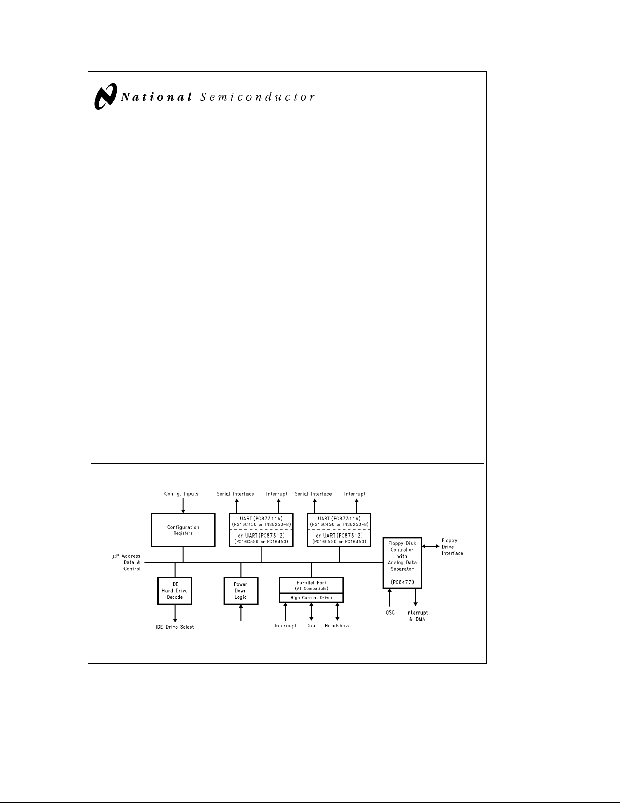
The PC87311A/12 incorporates a floppy disk controller
(FDC), two full function UARTs, a bidirectional parallel port,
and IDE interface control logic in one chip. The PC87311A
includes standard AT/XT address decoding for on-chip
functions and a Configuration Register, offering a single
chip solution to the most commonly used IBM
PC-XT
, and PC-ATÉperipherals. The PC87312 includes
É
standard AT address decoding for on-chip functions and a
Configuration Register set, offering a single chip solution to
the most commonly used ISA, EISA and Micro Channel peripherals.
The on-chip FDC is software compatible to the PC8477,
which contains a superset of the DP8473 and NEC mPD765
and the N82077 floppy disk controller functions. The onchip analog data separator requires no external components and supports the 4 Mb drive format as well as the
other standard floppy drives used with 5.25
dia.
In the PC87311A, the UARTs are equivalent to two
INS8250N-Bs or NS16450s. The bidirectional parallel port
maintains complete compatibility with the IBM PC, XT and
AT. In the PC87312 the UARTs are equivalent to two
NS16450s or PC16550s. The bidirectional parallel port
maintains complete compatibility with the ISA, EISA and Micro Channel parallel ports.
The IDE control logic provides a complete IDE interface except for the signal buffers. The Configuration Registers consist of three byte-wide registers. An Index and a Data Register which can be relocated within the ISA I/O address space
access the Configuration Registers.
ÉPCÉ
and 3.5×me-
×
Features
Y
100% compatible with IBM PC, XT, and AT architectures (PC87311A), or ISA, EISA, and Micro Channel architectures (PC87312)
Y
FDC:
Ð Software compatible with the DP8473, the 765A and
,
the N82077
Ð 16-byte FIFO (default disabled)
Ð Burst and Non-Burst modes
Ð Perpendicular Recording drive support
Ð High performance internal analog data separator (no
external filter components required)
Ð Low power CMOS with power down mode
Y
UARTs:
Ð Software compatible with the INS8250N-B and the
NS16450 (PC87311A), or PC16550A and PC16450
(PC87312)
Y
Parallel Port:
Ð Bidirectional under either software or hardware
control
Ð Compatible with all IBM PC, XT and AT architectures
(PC87311A), or all ISA, EISA, and Micro Channel ar-
chitectures (PC87312)
Ð Back Voltage protection circuit against damage
caused when printer is powered up
Y
IDE Control Logic:
Ð Provides a complete IDE interface except for option-
al buffers
Y
Address Decoder:
Ð Provides selection of all primary and secondary ISA
addresses including COM 1 –4.
Y
100-pin PQFP package
Ð The PC87311A and PC87312 are pin compatible
October 1993
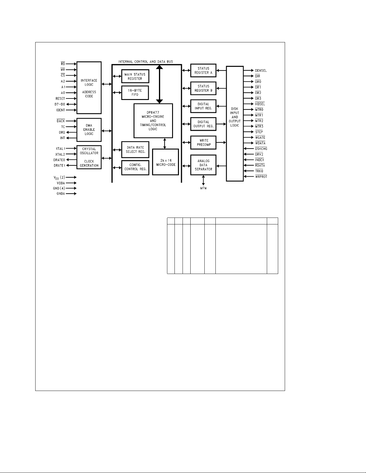
PC87311A/PC87312 (SuperI/O II/III) Floppy Disk Controller
with Dual UARTs, Parallel Port, and IDE Interface
Block Diagram
TL/F/11362– 1
TRI-STATEÉis a registered trademark of National Semiconductor Corporation.
TM
SuperI/O
is a trademark of National Semiconductor Corporation.
IBM
,PCÉ, PC-ATÉ, PC-XTÉand PS/2Éare registered trademarks of International Business Machines Corporation.
É
C
1995 National Semiconductor Corporation RRD-B30M75/Printed in U. S. A.
TL/F/11362
Page 2

Table of Contents
1.0 PIN DESCRIPTION ААААААААААААААААААААААААААААААА6
2.0 CONFIGURATION REGISTERS АААААААААААААААААА12
2.1 Overview ААААААААААААААААААААААААААААААААААААА12
2.2 Software Configuration ААААААААААААААААААААААААА12
2.3 Hardware Configuration АААААААААААААААААААААААА12
2.4 Index and Data Registers ААААААААААААААААААААААА14
2.5 Base Configuration Registers ААААААААААААААААААА14
2.5.1 Function Enable Register (FER) АААААААААААА14
2.5.2 Function Address Register (FAR) ААААААААААА16
2.5.3 Power and Test Register (PTR)ААААААААААААА16
2.6 Power Down Options АААААААААААААААААААААААААА16
2.7 Power Up Procedure and Considerations ААААААААА17
2.7.1 Crystal Stabilization ААААААААААААААААААААААА17
2.7.2 UART Power-Up ААААААААААААААААААААААААА17
2.7.3 FDC Power-Up ААААААААААААААААААААААААААА17
3.0 FDC REGISTER DESCRIPTION АААААААААААААААААА17
3.1 Status Register A (SRA) АААААААААААААААААААААААА18
3.1.1 SRAРPS/2 Mode АААААААААААААААААААААААА19
3.1.2 SRAРModel 30 Mode АААААААААААААААААААА19
3.2 Status Register B (SRB) АААААААААААААААААААААААА19
3.2.1 SRBРPS/2 Mode АААААААААААААААААААААААА19
3.2.2 SRBРModel 30 Mode АААААААААААААААААААА19
3.3 Digital Output Register (DOR) ААААААААААААААААААА20
3.4 Tape Drive Register (TDR)АААААААААААААААААААААА20
3.5 Main Status Register (MSR) АААААААААААААААААААА20
3.6 Data Rate Select Register (DSR) АААААААААААААААА21
3.7 Data Register (FIFO)ААААААААААААААААААААААААААА22
3.8 Digital Input Register (DIR) ААААААААААААААААААААА22
3.8.1 DIRРPC-AT Mode ААААААААААААААААААААААА22
3.8.2 DIRРPS/2 Mode АААААААААААААААААААААААА22
3.8.3 DIRРModel 30 Mode ААААААААААААААААААААА22
3.9 Configuration Control Register (CCR) АААААААААААА23
3.9.1 CCRРPC-AT and PS/2 Modes АААААААААААА23
3.9.2 CCRРModel 30 Mode АААААААААААААААААААА23
3.10 Result Phase Status Registers ААААААААААААААААА23
3.10.1 Status Register 0 (ST0) ААААААААААААААААА23
3.10.2 Status Register 1 (ST1) ААААААААААААААААА23
3.10.3 Status Register 2 (ST2) ААААААААААААААААА24
3.10.4 Status Register 3 (ST3) ААААААААААААААААА24
4.0 FDC COMMAND SET DESCRIPTION ААААААААААААА24
4.1 Command Set Summary ААААААААААААААААААААААА24
4.2 Command Description ААААААААААААААААААААААААА28
4.2.1 Configure Command АААААААААААААААААААААА28
4.2.2 Dumpreg Command АААААААААААААААААААААА29
4.2.3 Format Track CommandААААААААААААААААААА29
4.2.4 Invalid CommandААААААААААААААААААААААААА32
4.2.5 Lock Command АААААААААААААААААААААААААА32
4.2.6 Mode Command ААААААААААААААААААААААААА32
4.2.7 NSC Command АААААААААААААААААААААААААА33
4.2.8 Perpendicular Mode CommandААААААААААААА33
4.2.9 Read Data Command ААААААААААААААААААААА34
4.2.10 Read Deleted Data Command АААААААААА36
4.2.11 Read ID Command АААААААААААААААААААА36
4.2.12 Read A Track Command ААААААААААААААА36
4.2.13 Recalibrate Command ААААААААААААААААА36
4.2.14 Relative Seek Command ААААААААААААААА36
4.2.15 Scan CommandsАААААААААААААААААААААА37
4.2.16 Seek CommandААААААААААААААААААААААА37
4.2.17 Sense Drive Status Command АААААААААА37
4.2.18 Sense Interrupt Command ААААААААААААА37
4.2.19 Set Track CommandААААААААААААААААААА38
4.2.20 Specify CommandААААААААААААААААААААА38
4.2.21 Verify Command АААААААААААААААААААААА39
4.2.22 Version Command АААААААААААААААААААА39
4.2.23 Write Data Command АААААААААААААААААА39
4.2.24 Write Deleted Data Command АААААААААА40
5.0 FDC FUNCTIONAL DESCRIPTION ААААААААААААААА40
5.1 Microprocessor InterfaceАААААААААААААААААААААА40
5.2 Modes of Operation АААААААААААААААААААААААААА41
5.3 Controller Phases АААААААААААААААААААААААААААА41
5.3.1 Command PhaseАААААААААААААААААААААААА41
5.3.2 Execution Phase АААААААААААААААААААААААА41
5.3.2.1 DMA ModeРFIFO Disabled ААААААА41
5.3.2.2 DMA ModeРFIFO Enabled АААААААА42
5.3.2.3 Interrupt ModeÐFIFO Disabled ÀÀÀÀ42
5.3.2.4 Interrupt ModeРFIFO Enabled ААААА43
5.3.2.5 Software Polling АААААААААААААААААА43
5.3.3 Result Phase ААААААААААААААААААААААААААА43
5.3.4 Idle PhaseАААААААААААААААААААААААААААААА43
5.3.5 Drive Polling Phase АААААААААААААААААААААА43
5.4 Data Separator АААААААААААААААААААААААААААААА43
5.5 Crystal Oscillator ААААААААААААААААААААААААААААА45
5.6 Perpendicular Recording Mode АААААААААААААААА46
5.7 Data Rate Selection АААААААААААААААААААААААААА47
5.8 Write Precompensation ААААААААААААААААААААААА47
5.9 FDC Low Power Mode LogicААААААААААААААААААА47
5.10 Reset Operation ААААААААААААААААААААААААААААА47
6.0 SERIAL PORTS АААААААААААААААААААААААААААААААА48
6.1 Introduction АААААААААААААААААААААААААААААААААА48
6.2 PC87311A Serial Ports ААААААААААААААААААААААААА48
6.2.1 Serial Port Registers АААААААААААААААААААААА48
6.2.2 Line Control Register (LCR)АААААААААААААААА48
6.2.3 Programmable Baud Rate GeneratorАААААААА51
6.2.4 Line Status Register (LSR)ААААААААААААААААА51
6.2.5 Interrupt Identification Register (IIR) АААААААА52
6.2.6 Interrupt Enable Register (IER) ААААААААААААА52
6.2.7 MODEM Control Register (MCR) ААААААААААА52
6.2.8 MODEM Status Register (MSR) АААААААААААА53
6.2.9 Scratchpad Register (SCR) АААААААААААААААА53
6.3 PC87312 Serial Ports АААААААААААААААААААААААААА53
6.3.1 Serial Port Registers АААААААААААААААААААААА53
6.3.2 Line Control Register (LCR)АААААААААААААААА53
6.3.3 Programmable Baud Rate GeneratorАААААААА56
2
Page 3

Table of Contents
6.3.4 Line Status Register (LSR) ААААААААААААААА56
6.3.5 FIFO Control Register (FCR)АААААААААААААА57
6.3.6 Interrupt Identification Register (IIR) ААААААА57
6.3.7 Interrupt Enable Register (IER) АААААААААААА57
6.3.8 MODEM Control Register (MCR) АААААААААА58
6.3.9 MODEM Status Register (MSR) ААААААААААА59
6.3.10 Scratchpad Register (SCR) ААААААААААААААА59
7.0 PARALLEL PORT АААААААААААААААААААААААААААААА59
7.1 Introduction АААААААААААААААААААААААААААААААААА59
7.2 Data Register (DTR) ААААААААААААААААААААААААААА60
7.3 Status Register (STR) АААААААААААААААААААААААААА60
7.4 Control Register (CTR) ААААААААААААААААААААААААА60
8.0 INTEGRATED DEVICE ELECTRONICS
INTERFACE (IDE) АААААААААААААААААААААААААААААА61
8.1 Introduction АААААААААААААААААААААААААААААААААА61
8.2 IDE Signals ААААААААААААААААААААААААААААААААААА61
9.0 DEVICE DESCRIPTION ААААААААААААААААААААААААА62
9.1 DC Electrical Characteristics АААААААААААААААААААА62
9.2 AC Electrical Characteristics АААААААААААААААААААА64
9.2.1 AC Test Conditions АААААААААААААААААААААА64
9.2.2 Clock Timing ААААААААААААААААААААААААААА64
9.2.3 Microprocessor Interface Timing АААААААААА65
9.2.4 Baudout Timing ААААААААААААААААААААААААА66
9.2.5 Transmitter Timing АААААААААААААААААААААА67
9.2.6 Receiver TimingААААААААААААААААААААААААА68
9.2.7 MODEM Control Timing АААААААААААААААААА69
9.2.8 DMA Timing АААААААААААААААААААААААААААА70
9.2.9 Reset Timing ААААААААААААААААААААААААААА71
9.2.10 Write Data Timing ААААААААААААААААААААААА71
9.2.11 Drive Control Timing ААААААААААААААААААААА72
9.2.12 Read Data Timing ААААААААААААААААААААААА72
9.2.13 IDE Timing ААААААААААААААААААААААААААААА72
9.2.14 Parallel Port Timing АААААААААААААААААААААА73
10.0 REFERENCE SECTION АААААААААААААААААААААААА74
10.1 Mnemonic Definitions for FDC Commands ААААААА74
10.2 Example Four Drive Circuit
Using the PC87311A/12 АААААААААААААААААААА75
List of Figures
FIGURE 2-1 PC87311A/87312 Configuration Registers АААААААААААААААААААААААААААААААААААААААААААААААААААААААААА12
FIGURE 3-1 FDC Functional Block DiagramААААААААААААААААААААААААААААААААААААААААААААААААААААААААААААААААААААА18
FIGURE 4-1 IBM, Perpendicular, and ISO Formats Supported by Format Command АААААААААААААААААААААААААААААААААА30
FIGURE 5-1 FDC Data Separator Block Diagram АААААААААААААААААААААААААААААААААААААААААААААААААААААААААААААААА44
FIGURE 5-2 PC87311A/87312 Dynamic Window Margin Performance ААААААААААААААААААААААААААААААААААААААААААААА45
FIGURE 5-3 Read Data AlgorithmРState DiagramААААААААААААААААААААААААААААААААААААААААААААААААААААААААААААААА46
FIGURE 5-4 Perpendicular Recording Drive R/W Head and Pre-Erase Head АААААААААААААААААААААААААААААААААААААААА46
FIGURE 6-1 PC87311A Composite Serial Data АААААААААААААААААААААААААААААААААААААААААААААААААААААААААААААААААА48
FIGURE 6-2 PC87312 Composite Serial Data ААААААААААААААААААААААААААААААААААААААААААААААААААААААААААААААААААА54
FIGURE 9-1 Clock Timing АААААААААААААААААААААААААААААААААААААААААААААААААААААААААААААААААААААААААААААААААААА64
FIGURE 9-2 Microprocessor Read Timing АААААААААААААААААААААААААААААААААААААААААААААААААААААААААААААААААААААА65
FIGURE 9-3 Microprocessor Write Timing АААААААААААААААААААААААААААААААААААААААААААААААААААААААААААААААААААААА66
FIGURE 9-4 Baudout Timing АААААААААААААААААААААААААААААААААААААААААААААААААААААААААААААААААААААААААААААААААА66
FIGURE 9-5 Transmitter Timing ААААААААААААААААААААААААААААААААААААААААААААААААААААААААААААААААААААААААААААААА67
FIGURE 9-6a Receiver TimingАААААААААААААААААААААААААААААААААААААААААААААААААААААААААААААААААААААААААААААААААА68
FIGURE 9-6b PC87312 FIFO Mode Receiver Timing АААААААААААААААААААААААААААААААААААААААААААААААААААААААААААААА68
FIGURE 9-6c PC87312 Timeout Receiver Timing ААААААААААААААААААААААААААААААААААААААААААААААААААААААААААААААААА69
FIGURE 9-7 MODEM Control Timing ААААААААААААААААААААААААААААААААААААААААААААААААААААААААААААААААААААААААААА69
FIGURE 9-8 DMA Timing ААААААААААААААААААААААААААААААААААААААААААААААААААААААААААААААААААААААААААААААААААААА70
FIGURE 9-9 Reset Timing АААААААААААААААААААААААААААААААААААААААААААААААААААААААААААААААААААААААААААААААААААА71
FIGURE 9-10 Write Data Timing АААААААААААААААААААААААААААААААААААААААААААААААААААААААААААААААААААААААААААААААА71
FIGURE 9-11 Drive Control Timing АААААААААААААААААААААААААААААААААААААААААААААААААААААААААААААААААААААААААААААА72
FIGURE 9-12 Read Data Timing АААААААААААААААААААААААААААААААААААААААААААААААААААААААААААААААААААААААААААААААА72
FIGURE 9-13 IDE Timing АААААААААААААААААААААААААААААААААААААААААААААААААААААААААААААААААААААААААААААААААААААА72
FIGURE 9-14 Parallel Port Interrupt Timing (Compatible Mode) ААААААААААААААААААААААААААААААААААААААААААААААААААААА73
FIGURE 9-15 Parallel Port Interrupt Timing (Extended Mode) ААААААААААААААААААААААААААААААААААААААААААААААААААААААА73
FIGURE 9-16 Typical Parallel Port Data Exchange АААААААААААААААААААААААААААААААААААААААААААААААААААААААААААААААА73
FIGURE 10-1 PC87311A/87312 Four Floppy Drive Circuit ААААААААААААААААААААААААААААААААААААААААААААААААААААААААА75
FIGURE 10-2 IDE Interface Signal Equations ААААААААААААААААААААААААААААААААААААААААААААААААААААААААААААААААААААА75
FIGURE 10-3 PC87311A/87312 Adapter Card Schematic ААААААААААААААААААААААААААААААААААААААААААААААААААААААААА76
3
Page 4

List of Tables
TABLE 2-1 Default Configurations Controlled by Hardware АААААААААААААААААААААААААААААААААААААААААААААААААААААААА13
TABLE 2-2 Index and Data Register Optional Locations ААААААААААААААААААААААААААААААААААААААААААААААААААААААААААА14
TABLE 2-3 Primary and Secondary Drive Address Selection ААААААААААААААААААААААААААААААААААААААААААААААААААААААА15
TABLE 2-4 Encoded Drive and Motor Pin Information ААААААААААААААААААААААААААААААААААААААААААААААААААААААААААААА15
TABLE 2-5 Parallel Port AddressesААААААААААААААААААААААААААААААААААААААААААААААААААААААААААААААААААААААААААААА16
TABLE 2-6a COM Port Selection for UART1 АААААААААААААААААААААААААААААААААААААААААААААААААААААААААААААААААААААА16
TABLE 2-6b COM Port Selection for UART2 АААААААААААААААААААААААААААААААААААААААААААААААААААААААААААААААААААААА16
TABLE 2-7 Address Selection for COM3 and COM4 АААААААААААААААААААААААААААААААААААААААААААААААААААААААААААААА16
TABLE 3-1 Register Description and AddressesАААААААААААААААААААААААААААААААААААААААААААААААААААААААААААААААААА18
TABLE 3-2 Drive Enable Values ААААААААААААААААААААААААААААААААААААААААААААААААААААААААААААААААААААААААААААААА20
TABLE 3-3 Tape Drive Assignment Values АААААААААААААААААААААААААААААААААААААААААААААААААААААААААААААААААААААА20
TABLE 3-4 Write Precompensation Delays АААААААААААААААААААААААААААААААААААААААААААААААААААААААААААААААААААААА21
TABLE 3-5 Default Precompensation Delays АААААААААААААААААААААААААААААААААААААААААААААААААААААААААААААААААААА21
TABLE 3-6 Data Rate Select Encoding ААААААААААААААААААААААААААААААААААААААААААААААААААААААААААААААААААААААААА22
TABLE 4-1 Typical Format Gap Length ValuesААААААААААААААААААААААААААААААААААААААААААААААААААААААААААААААААААА31
TABLE 4-2 DENSEL EncodingААААААААААААААААААААААААААААААААААААААААААААААААААААААААААААААААААААААААААААААААА33
TABLE 4-3 DENSEL Default EncodingАААААААААААААААААААААААААААААААААААААААААААААААААААААААААААААААААААААААААА33
TABLE 4-4 Effect of Drive Mode and Data Rate on Format and Write CommandsААААААААААААААААААААААААААААААААААААА34
TABLE 4-4a Effect of GAP and WG on Format and Write Commands АААААААААААААААААААААААААААААААААААААААААААААААА34
TABLE 4-5 Sector Size Selection АААААААААААААААААААААААААААААААААААААААААААААААААААААААААААААААААААААААААААААА34
TABLE 4-6 SK Effect on Read Data CommandААААААААААААААААААААААААААААААААААААААААААААААААААААААААААААААААААА35
TABLE 4-7 Result Phase Termination Values with No Error АААААААААААААААААААААААААААААААААААААААААААААААААААААААА35
TABLE 4-8 SK Effect on Read Deleted Data Command ААААААААААААААААААААААААААААААААААААААААААААААААААААААААААА36
TABLE 4-9 Maximum Recalibrate Step Pulses Based on R255 and ETRААААААААААААААААААААААААААААААААААААААААААААА36
TABLE 4-10 Scan Command Termination Values ААААААААААААААААААААААААААААААААААААААААААААААААААААААААААААААААА37
TABLE 4-11 Status Register 0 Termination Codes ААААААААААААААААААААААААААААААААААААААААААААААААААААААААААААААААА38
TABLE 4-12 Set Track Register Address ААААААААААААААААААААААААААААААААААААААААААААААААААААААААААААААААААААААААА38
TABLE 4-13 Step Rate (SRT) Values АААААААААААААААААААААААААААААААААААААААААААААААААААААААААААААААААААААААААААА38
TABLE 4-14 Motor Off Time (MFT) ValuesАААААААААААААААААААААААААААААААААААААААААААААААААААААААААААААААААААААААА39
TABLE 4-15 Motor On Time (MNT) Values ААААААААААААААААААААААААААААААААААААААААААААААААААААААААААААААААААААААА39
TABLE 4-16 Verify Command Result Phase Table ААААААААААААААААААААААААААААААААААААААААААААААААААААААААААААААААА40
TABLE 6-1 PC87311A UART Register Addresses (AEN
TABLE 6-2 PC87311A Register Summary for an Individual UART ChannelААААААААААААААААААААААААААААААААААААААААААА49
TABLE 6-3 PC87311A UART Reset ConfigurationАААААААААААААААААААААААААААААААААААААААААААААААААААААААААААААААА50
TABLE 6-4 PC87311A UART Divisors, Baud Rates, and Clock Frequencies ААААААААААААААААААААААААААААААААААААААААА51
TABLE 6-5 PC87311A Interrupt Control FunctionsАААААААААААААААААААААААААААААААААААААААААААААААААААААААААААААААА52
TABLE 6-6 PC87312 UART Register Addresses (AEN
TABLE 6-7 PC87312 Register Summary for an Individual UART Channel АААААААААААААААААААААААААААААААААААААААААААА54
TABLE 6-8 PC87312 UART Reset Configuration ААААААААААААААААААААААААААААААААААААААААААААААААААААААААААААААААА55
TABLE 6-9 PC87312 UART Divisors, Baud Rates, and Clock Frequencies ААААААААААААААААААААААААААААААААААААААААААА56
TABLE 6-10 PC87312 Interrupt Control Functions ААААААААААААААААААААААААААААААААААААААААААААААААААААААААААААААААА58
TABLE 7-1 Parallel Interface Register Addresses АААААААААААААААААААААААААААААААААААААААААААААААААААААААААААААААА59
TABLE 7-2 Data Register Read and Write Modes АААААААААААААААААААААААААААААААААААААААААААААААААААААААААААААААА59
TABLE 7-3 Parallel Port Mode of Operation ААААААААААААААААААААААААААААААААААААААААААААААААААААААААААААААААААААА59
TABLE 7-4 Parallel Port Reset StatesААААААААААААААААААААААААААААААААААААААААААААААААААААААААААААААААААААААААААА60
TABLE 8-1 IDE Registers and Their ISA AddressesААААААААААААААААААААААААААААААААААААААААААААААААААААААААААААААА61
TABLE 9-1 Nominal t
TABLE 9-2 Minimum t
TABLE 10-1 PC87311A/87312 Four Floppy Drive Encoding АААААААААААААААААААААААААААААААААААААААААААААААААААААААА75
Values АААААААААААААААААААААААААААААААААААААААААААААААААААААААААААААААААААААААААА64
ICP,tDRP
Values ААААААААААААААААААААААААААААААААААААААААААААААААААААААААААААААААААААААААААААА71
WDW
e
0) АААААААААААААААААААААААААААААААААААААААААААААААААААААА48
e
0) ААААААААААААААААААААААААААААААААААААААААААААААААААААААА53
4
Page 5
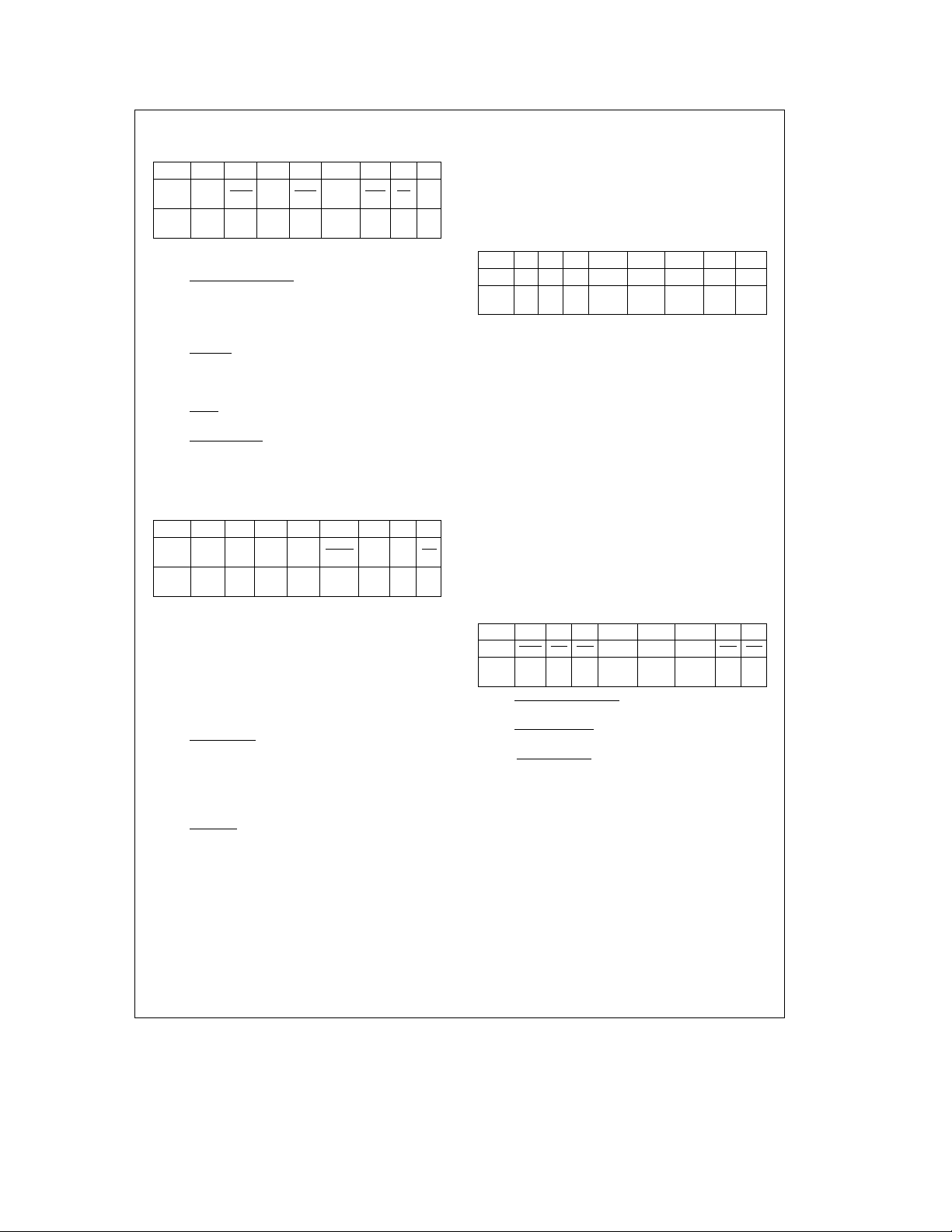
Basic Configuration
*Note: PC87311A only
TL/F/11362– 2
5
Page 6
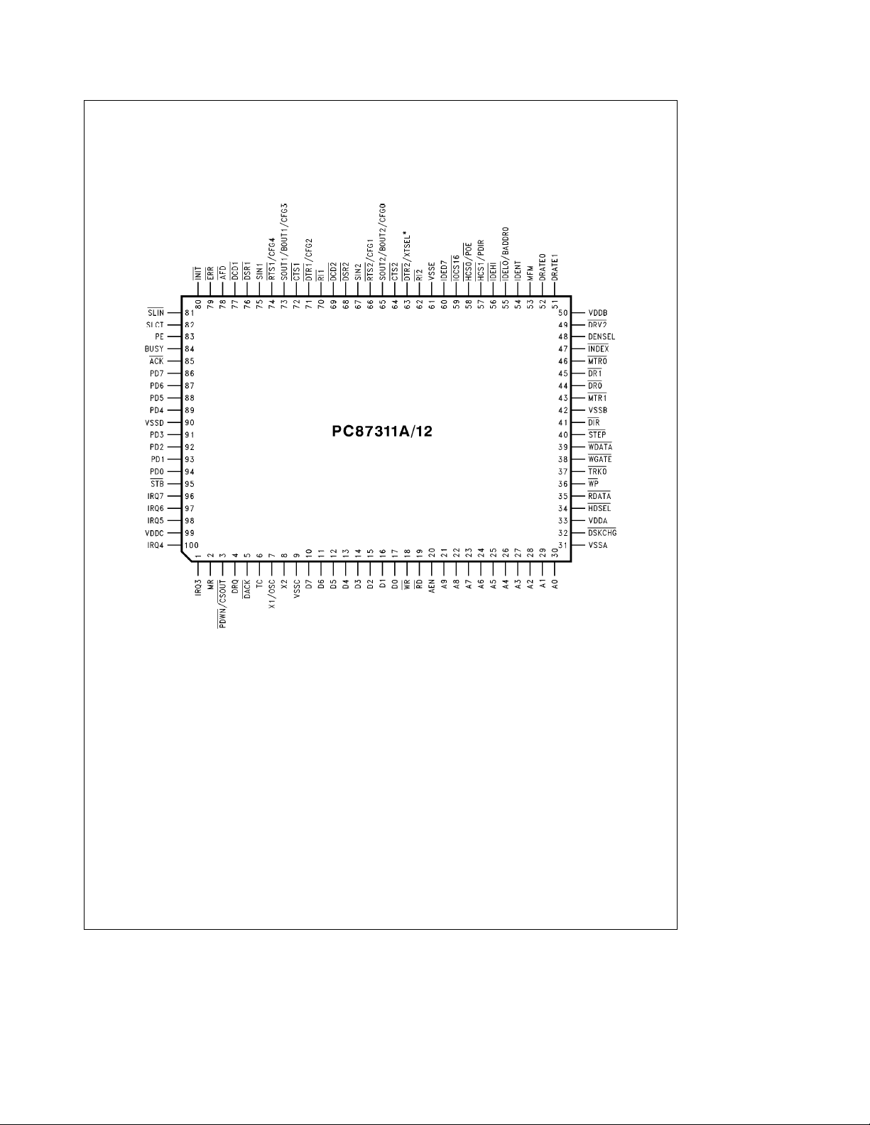
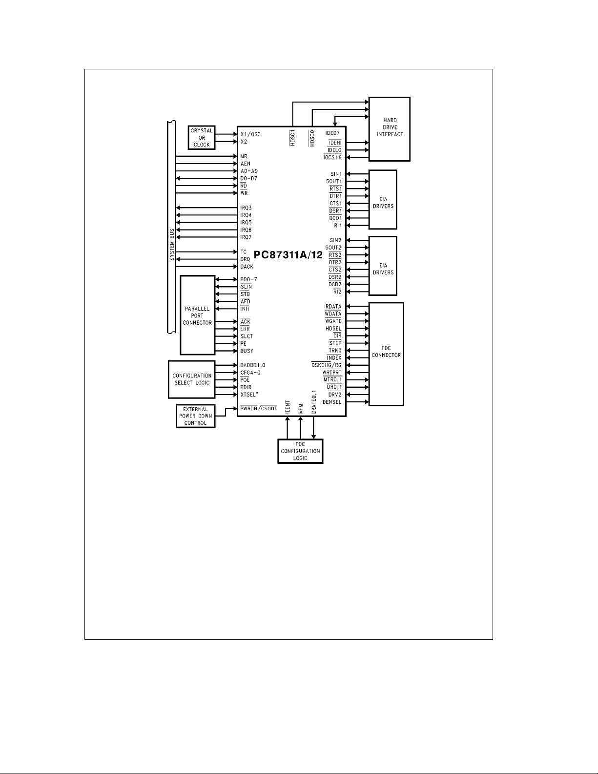
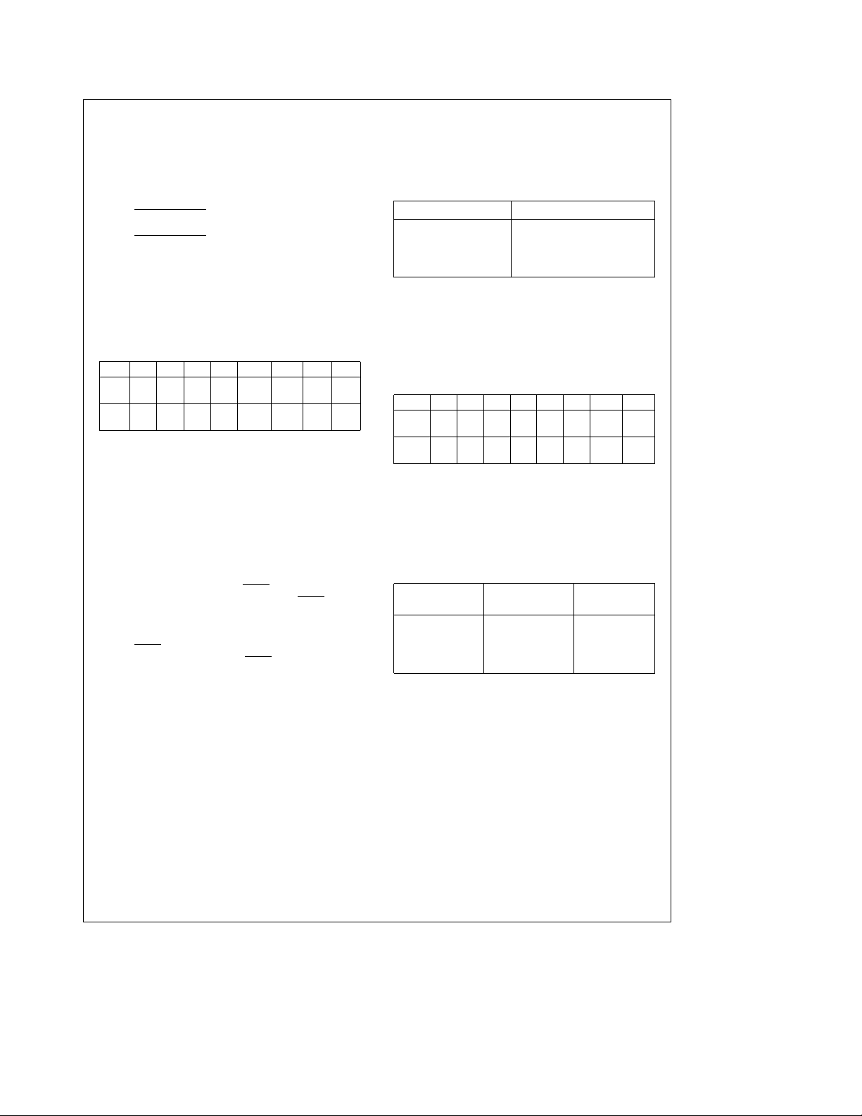
1.0 Pin Description
Connection Diagram
Plastic Quad Flatpak, EIAJ
*Note: XTSEL PC87311A only TL/F/11362– 3
Order Number PC87311AVF or PC87312VF
See NS Package Number VLJ100A
6
Page 7
1.0 Pin Description (Continued)
Symbol Pin I/O Function
A9–A0 21–30 I Address. These address lines from the microprocessor determine which internal register is accessed.
ACK 85 I Acknowledge. This input is pulsed low by the printer to indicate that it has received data from the
AFD 78 O Automatic Feed XT. When this signal is low the printer should automatically line feed after each line is
AEN 20 I Address Enable. This input disables function selection via A9 – A0 when it is high. Access to the FDC
BADDR0 55 I Base Address. This bit determines one of two base addresses from which the Index and Data
BOUT1,2 73, 65 O BAUD Output. This multi-function pin provides the associated serial channel Baud Rate generator
BUSY 84 I Busy. This pin is set high by the printer when it can’t accept another character. This pin has a nominal
CFG0–4 65, 66, I Default Configuration. These CMOS inputs select 1 of 32 default configurations in which the
71, 73,
74
CSOUT 3OChip Select Output. When the associated bit in the Power and Test Configuration Register is set, this
CTS1,2 72, 64 I Clear to Send. When low, this indicates that the MODEM or data set is ready to exchange data. The
D7–D0 10–17 I/O Data. Bi-directional data lines to the microprocessor. D0 is the LSB and D7 is the MSB. These signals
DACK 5IDMA Acknowledge. Active low input to acknowledge the FDC DMA request and enable the RD and
DCD1,2 77, 69 I Data Carrier Detect. When low, this indicates that the data carrier has been detected by the MODEM
DENSEL 48 O Density Select. Indicates when a high FDC density data rate (500 kb/s or 1 Mb/s) or a low density
DIR 41 O Direction. This output determines the direction of the floppy disk drive (FDD) head movement (active
A0–A9 are don’t cares during an FDC DMA transfer.
parallel port. This pin has a nominal 25 kX pull-up resistor attached.
printed. This pin will be in a TRI-STATEÉcondition 10 ns after a zero is loaded into the corresponding
Control Register bit. The system should pull this pin high using a 4.7 kX resistor.
Data Register during DMA transfer is NOT affected by this pin.
Registers will be offset (see Table 2-2). An internal pull-down resistor of 40 kX is on each pin. Use a
10 kX resistor to pull this pin to the required level during reset.
output signal, if test mode is selected in the Power and Test Configuration Register and the DLAB bit
(LCR7) is set. After Master Reset this pin provides the SOUT function. (See SOUT and CFG0–4 for
further information.)
25 kX pull-down resistor attached to it.
PC87311A/12 will power-up (see Table 2-1). An internal pull-down resistor of 40 kX is on each pin.
Usea10kXresistor to pull these pins to the required level during reset.
multi-function pin provides an active signal each time the internal address decoder decodes an
address enabled for the PC87311A/12. (See PWDN
CTS
signal is a MODEM status input whose condition the CPU can test by reading bit 4 (CTS) of the
MODEM Status Register (MSR) for the appropriate serial channel. Bit 4 is the complement of the CTS
signal. Bit 0 (DCTS) of the MSR indicates whether the CTS input has changed state since the previous
reading of the MSR. CTS
Note: Whenever the DCTS bit of the MSR is set an interrupt is generated if MODEM Status interrupts are enabled.
all have 24 mA (sink) buffered outputs.
WR
inputs during a DMA transfer. When in PC-AT or Model 30 mode, this signal is enabled by bit D3 of
the Digital Output Register (DOR). When in PS/2Émode, DACK is always enabled, and bit D3 of the
DOR is reserved. DACK
or data set. The DCD
7 (DCD) of the MODEM Status Register (MSR) for the appropriate serial channel. Bit 7 is the
complement of the DCD
changed state since the previous reading of the MSR.
Note: Whenever the DDCD bit of the MSR is set, an interrupt is generated if MODEM Status interrupts are enabled.
data rate (250 or 300 kb/s) has been selected. DENSEL is active high for high density (5.25
when IDENT is high, and active low for high density (3.5
programmable via the Mode command (see Section 4.2.6).
e
step in, inactiveestep out) during a seek operation. During read or writes, DIR will be inactive.
has no effect on the transmitter.
should be held high during PIO accesses.
signal is a MODEM status input whose condition the CPU can test by reading bit
signal. Bit 3 (DDCD) of the MSR indicates whether the DCD input has
for further information.)
drives) when IDENT is low. DENSEL is also
×
drives)
×
7
Page 8
1.0 Pin Description (Continued)
Symbol Pin I/O Function
DR0,1 44, 45 O Drive Select 0,1. These are the decoded drive select outputs that are controlled by Digital Output
DRATE0,1 52, 51 O Data Rate 0,1. These outputs reflect the currently selected FDC data rate, (bits 0 and 1 in the
DRQ 4 O DMA Request. Active high output to signal the DMA controller that a FDC data transfer is needed.
DRV2 49 I Drive2. This input indicates whether a second disk drive has been installed. The state of this pin is
DSKCHG 32 I Disk Change. The input indicates if the drive door has been opened. The state of this pin is available
DSR1,2 76, 68 I Data Set Ready. When low, this indicates that the data set or MODEM is ready to establish a
DTR1,2 71, 63 O Data Terminal Ready. When low, this output indicates to the MODEM or data set that the UART is
ERR 79 I Error. This input is set low by the printer when it has detected an error. This pin has nominal 25 kX
HCS0 58 O Hard Drive Chip Select 0. This output is active in the AT mode when the hard drive registers from
HCS1 57 O Hard Drive Chip Select 1. This output is active in the AT mode when the hard drive registers from
HDSEL 34 O Head Select. This output determines which side of the FDD is accessed. Active selects side 1,
IDED7 60 I/O IDE Bit 7. This pin provides the data bus bit 7 signal to the IDE hard drive during accesses in the
IDEHI 56 O IDE High Byte. This output enables the high byte data latch during a read or write to the hard drive if
IDELO 55 O IDE Low Byte. This output enables the low byte data latch during a read or write to the hard drive .
Register bits D0, D1. The Drive Select outputs are gated with DOR bits 4–7. These are active low
outputs. They are encoded with information to control four FDDs when bit 4 of the Function Enable
Register (FER) is set. (See MTR0,1
Configuration Control Register (CCR) or the Data Rate Select Register (DSR), whichever was written
to last). These pins are totem-pole buffered outputs (6 mA sink, 6 mA source).
When in PC-AT or Model 30 mode, this signal is enabled by bit D3 of the DOR. When in PS/2 mode,
DRQ is always enabled, and bit D3 of the DOR is reserved.
available from Status Register A in PS/2 mode.
from the Digital Input register. This pin can also be configured as the RGATE data separator
diagnostic input via the Mode command (see Section 4.2.6).
communications link. The DSR
reading bit 5 (DSR) of the MODEM Status Register (MSR) for the appropriate channel. Bit 5 is the
complement of the DSR
changed state since the previous reading of the MSR.
Note: Whenever the DDSR bit of the MSR is set, an interrupt is generated if MODEM Status interrupts are enabled.
ready to establish a communications link. The DTR
bit 0 (DTR) of the MODEM Control Register to a high level. A Master Reset operation sets this signal
to its inactive (high) state. In the PC87312, loop mode operation holds this signal to its inactive state.
(See CFG4–0 for further information.) In the PC87311A, loop mode operation holds this signal to its
inactive state if the XTSEL pin is high during reset. If the XTSEL pin is low during reset, the associated
pin state is controlled by the MCR0 bit during loop mode operation. (See XTSEL and CFG0–4 for
further information.)
pull-up resistor attached to it.
1F0–1F7h are selected if the primary address is used or when 170 – 177h are selected if the
secondary address is used. In the XT mode (PC87311A) this output is active if the addresses from
320–324h are selected. This output is inactive if the IDE interface is disabled via the Configuration
Register. (See POE for further information.)
3F6–7 are selected if the primary address is used or when 376 – 377 are selected if the secondary
address is used. In the XT mode (PC87311A) this output is inactive. This output is also inactive if the
IDE interface is disabled via the Configuration Register. (See PDIR for further information.)
inactive selects side 0.
address range 1F0–1F7h, 170 – 177h and 3F6h and 376h. This pin is TRI-STATE during read or write
accesses to 3F7h and 377h.
the hard drive returns IOCS16
Configuration Register.
This output is inactive if the IDE interface is disabled via the Configuration Register. (See BADDR0 for
further information.)
signal. Bit 1 (DDSR) of the MSR indicates whether the DSR input has
and Table 2-4 for more information.)
signal is a MODEM status input whose condition the CPU can test by
signal can be set to an active low by programming
. This output is inactive if the IDE interface is disabled via the
8
Page 9
1.0 Pin Description (Continued)
Symbol Pin I/O Function
IDENT 54 I Identity. During chip reset, the IDENT and MFM pins are sampled to determine the mode of operation
INDEX 47 I Index. This input signals the beginning of a FDD track.
INIT 80 O Initialize. When this signal is low it causes the printer to be initialized. This pin will be in a TRI-STATE
IOCS16 59 I I/O Chip Select 16-Bit. This input will be driven by the peripheral device when it can accommodate a
IRQ3,4 1, 100 O Interrupt 3 and 4. These are active high interrupts associated with the serial ports. IRQ3 presents the
IRQ5 98 O Interrupt 5. Active high output that indicates a parallel port interrupt. When enabled this bit follows the
IRQ6 97 O Interrupt 6. Active high output to signal the completion of the execution phase for certain FDC
IRQ7 96 O Interrupt 7. Active high output that indicates a parallel port interrupt. When enabled this bit follows the
MR 2 I Master Reset. Active high input that resets the controller to the idle state, and resets all disk interface
according to the following table:
IDENT MFM MODE
1 1 or NC PC-AT Mode
1 0 Illegal
0 1 or NC PS/2 Mode
0 0 Model 30 Mode
AT ModeÐThe DMA enable bit in the DOR is valid. TC is active high. Status Registers A and B are
disabled (TRI-STATE).
Model 30 ModeÐThe DMA enable bit in the DOR is valid. TC is active high. Status Registers A and B
are enabled.
PS/2 ModeÐThe DMA enable bit in the DOR is a don’t care, and the DRQ and IRQ6 signals will always
be enabled. TC is active low. Status Registers A and B are enabled.
After chip reset, the state of IDENT determines the polarity of the DENSEL output.
When IDENT is a logic ‘‘1’’, DENSEL is active high for the 500 kbs/1 Mbs data rates.
When IDENT is a logic ‘‘0’’, DENSEL is active low for the 500 kbs/1 Mbs data rates.
(See Mode command for further explanation of DENSEL.)
condition 10 ns after a zero is loaded into the corresponding Control Register bit. The system should pull
this pin high using a 4.7 kX resistor.
16-bit access.
signal if the serial channel has been designated as COM2 or COM4. IRQ4 presents the signal if the serial
port is designated as COM1 or COM3. The appropriate interrupt goes active whenever it is enabled via
IER, the associated Interrupt Enable bit (Modem Control Register bit 3, MCR3), and any of the following
conditions are active: Receiver Error, Receive Data available, Transmitter Holding Register Empty, or a
Modem Status Flag is set. The interrupt is reset low (inactive) after the appropriate interrupt service
routine is executed, after being disabled via the IER, or after a Master Reset. Either interrupt can be
disabled, putting them into TRI-STATE, by setting the MCR3 bit low.
ACK
signal input. When bit 4 in the parallel port Control Register is set and the parallel port address is
designated as shown in Table 2-5, this interrupt is enabled. When it is not enabled or when operating in
the XT mode this signal is TRI-STATE.
commands. Also used to signal when a data transfer is ready during a Non-DMA operation. When in
PC-AT or Model 30 mode, this signal is enabled by bit D3 of the DOR. When in PS/2 mode, IRQ6 is
always enabled, and bit D3 of the DOR is reserved.
ACK
signal input. When bit 4 in the parallel port Control Register is set and the parallel port address is
designated as shown in Table 2-5, this interrupt is enabled. When it is not enabled this signal is
TRI-STATE.
outputs to their inactive states. The DOR, DSR, CCR, Mode command, Configure command, and Lock
command parameters are cleared to their default values. The Specify command parameters are not
affected. The Configuration Registers are set to their selected default values.
9
Page 10
1.0 Pin Description (Continued)
Symbol Pin I/O Function
MFM 53 I/O MFM. During a chip reset when in PS/2 mode (IDENT low), this pin is sampled to select the PS/2 mode
MTR0,1 46, 43 O Motor Select 0,1. These are the motor enable lines for drives 0 and 1, and are controlled by bits
PD0–7 94– 91, I/O Parallel Port Data. These bidirectional pins transfer data to and from the peripheral data bus and the
89–86
PDIR 57 I Parallel Port Direction. During reset the state of this pin determines the direction of the parallel port
PDWN 3IPower Down. This multi-function pin will stop the clocks and/or the external crystal based on the
PE 83 I Paper End. This input is set high by the printer when it is out of paper. This pin has a nominal 25 kX
POE 58 I Parallel Port Output Enable. This pin is sensed during reset. If it is low, bit 7 of the Power and Test
RD 19 I Read. Active low input to signal a data read by the microprocessor.
RDATA 35 I Read Data. This input is the raw serial data read from the floppy disk drive.
RI1,2 70, 62 I Ring Indicator. When low this indicates that a telephone ringing signal has been received by the
RTS1,2 74, 66 O Request to Send. When low, this output indicates to the MODEM or data set that the UART is ready to
SIN1,2 75, 67 I Serial Input. This input receives composite serial data from the communications link (peripheral device,
SLCT 82 I Select. This input is set high by the printer when it is selected. This pin has a nominal 25 kX pull-down
SLIN 81 O Select Input. When this signal is low it selects the printer. This pin will be in a TRI-STATE condition
(MFM high), or the Model 30 mode (MFM low). An internal pull-up or external pull-down 10 kX resistor
will select between the two PS/2 modes. When the PC-AT mode is desired, (IDENT high), MFM should
be left pulled high internally. MFM reflects the current data encoding format when RESET is inactive.
e
MFM
high, FMelow. Defaults to low after a chip reset. This signal can also be configured as the
PUMP data separator diagnostic output via the Mode command (see Section 4.2.6).
D7–D4 of the Digital Output register. They are active low outputs. They are encoded with information to
control four FDDs when bit 4 of the Function Enable Register (FER) is set. (See DR0,1
for more information.)
parallel port Data Register. These pins have high current drive capability. (See DC Electrical
Characteristics.)
data, if the PTR7
input (scanner) when PDIR
Usea10kXresistor to pull this pin to the required level during reset.
selections made in the Power and Test Register bits 1-2. (See CSOUT for additional information.)
pull-down resistor attached to it.
Register (PTR7) is set high and the parallel port will operate in the Extended Mode. In this mode
software determines the direction of parallel port data via the parallel port Control Register (CTR5). If
this pin is high (PTR7
by the state of PDIR pin at reset. An internal pull-down resistor of 40 kX is on this pin. Use a 10 kX
resistor to pull this pin to the required level during reset.
MODEM. The RI
of the MODEM Status Register (MSR) for the appropriate serial channel. Bit 6 is the complement of the
RI
signal. Bit 2 (TERI) of the MSR indicates whether the RI input has changed from low to high since the
previous reading of the MSR.
Note: Whenever the TERI bit of the MSR is set, an interrupt is generated if MODEM Status interrupts are enabled.
exchange data. The RTS
Control Register to a high level. A Master Reset operation sets this signal to its inactive (high) state. In
the PC87312, loop mode operation holds this signal to its inactive state. (See CFG0–4 for further
information.) In the PC87311A, loop mode operation holds this signal to its inactive state if the XTSEL
pin is high during reset. If the XTSEL pin is low during reset, the associated pin state is controlled by the
MCR1 bit during loop mode operation. (See CFG0–4 for further information.)
MODEM, or data set).
resistor attached to it.
10 ns after a zero is loaded into the corresponding Control Register bit. The system should pull this pin
high using a 4.7 kX resistor.
e
0. The direction will be output (printer) when PDIRe0 and PTR7e0 and it will be
e
1 and PTR7e0. An internal pull-down resistor or 40 kX is on this pin.
e
0) then the Compatible Mode is selected and the data direction is determined
signal is a MODEM status input whose condition the CPU can test by reading bit 6 (RI)
signal can be set to an active low by programming bit 1 (RTS) of the MODEM
and Table 2-4
10
Page 11
1.0 Pin Description (Continued)
Symbol Pin I/O Function
SOUT1,2 73, 65 O Serial Output. This output sends composite serial data to the communications link (peripheral device,
STB 95 O Data Strobe. This output indicates to the printer that valid data is available at the printer port. This pin
STEP 40 O Step. This output signal issues pulses to the disk drive at a software programmable rate to move the
TC 6 I Terminal Count. Control signal from the DMA controller to indicate the termination of a DMA transfer.
TRK0 37 I Track 0. This input indicates to the controller that the head of the selected floppy disk drive is at track
VDDA 33 Analog Supply. This pin is the 5V supply for the analog data separator.
VDDB,C 50, 99 Digital Supply. This is the 5V supply voltage for the digital circuitry.
VSSA 31 Analog Ground. This is the analog ground for the data separator.
VSSB-E 42, 9, Digital Ground. This is the ground for the digital circuitry.
90, 61
WR 18 I Write. Active low input to signal a write from the microprocessor to the controller.
WDATA 39 O Write Data. This output is the write precompensated serial data that is written to the selected floppy
WGATE 38 O Write Gate. This output signal enables the write circuitry of the selected disk drive. WGATE has been
WP 36 I Write Protect. This input indicates that the disk in the selected drive is write protected.
X1/OSC 7 I Crystal1/Clock. One side of an external 24 MHz crystal is attached here. If a crystal is not used, a TTL
X2 8 O Crystal2. One side of an external 24 MHz crystal is attached here. This pin is left unconnected if an
XTSEL* 63 I XT Select. When this pin is high during reset the chip will operate in the XT mode. When this pin is low
*Note: XTSEL is an option for the PC87311A only.
MODEM, or data set). The SOUT signal is set to a marking state (logic 1) after a Master Reset
operation. (See BOUT and CFG0–4 for further information on these pins.)
will be in a TRI-STATE condition 10 ns after a zero is loaded into the corresponding Control Register bit.
The system should pull this pin high using a 4.7 kX resistor.
head during a seek operation.
TC is accepted only when DACK
low in PS/2 mode.
zero.
disk drive. Precompensation is software selectable.
designed to prevent glitches during power up and power down. This prevents writing to the disk when
power is cycled.
or CMOS compatible clock is connected to this pin.
external clock is used.
during reset the chip will operate in the AT mode. An internal pull-down resistor of 40 kX is on this pin.
Usea10kXresistor to pull this pin to the required level during reset.
There are five differences between AT and XT mode. One concerns hard disk operation and the other
four concern UART operation. In AT mode the IDE hard drive chip selects (HCS0
for addresses 1F0–7H and 3F6, 7H; respectively. In XT mode the IDE chip select HCS0
addresses 320–3H and HCS1
bit (see Section 6.5 bit 6), the modem control outputs during loop back mode (see Section 6.8 bit 4), the
Scratch Pad Register (see Section 6.10), and the availability of edge (XT) or level (AT) sensitive UART
interrupts.
is active. TC is active high in PC-AT and Model 30 modes, and active
, HCS1) will be active
responds to
is inactive. The differences in UART operation are: the function of LSR
11
Page 12
2.0 Configuration Registers
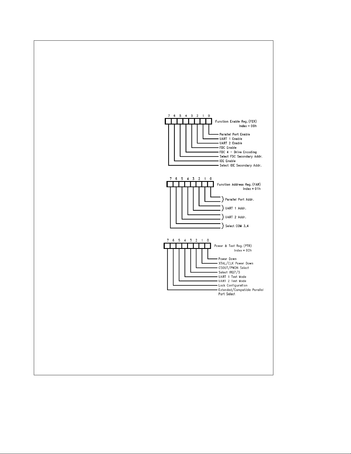
2.1 OVERVIEW
Three registers constitute the Base Configuration Register
set which controls the set-up of the PC87311A/12. In general, these registers control the enabling of each major
function (e.g., FDC, UARTs, parallel port, etc.), the I/O addresses of those functions, and whether those functions
power down via hardware control or not. These three configuration registers are called the Function Enable Register
(FER), the Function Address (FAR) Register and the Power
and Test Register (PTR).
These registers can be accessed via hardware or software.
During reset, the PC87311A/12 loads a set of default values selected by a hardware strapping option into the Configuration Registers. This defines the setting of all Configuration Registers via hardware.
An index and data register pair are used to read and write
these registers. Each Configuration Register is pointed to by
the value loaded into the Index Register. The data to be
written into the Configuration Register is transferred via the
Data register. Reading a Configuration Register is done in a
similar way (i.e., by pointing to it via the Index Register and
then reading its contents via the Data Register).
Accessing the Configuration Registers in this way requires
only two system I/O addresses. Since that I/O space is
shared by other devices the Index and Data Registers could
still be inadvertantly accessed, even though, there are only
two registers in this I/O address space. In order to reduce
the chances of an inadvertant access, a simple procedure
(Section 2.2) has been developed.
2.2 SOFTWARE CONFIGURATION
If the system requires access to the Configuration Registers
after reset, then the following procedure is used to change
data in the registers.
1. Determine the default location of the PC87311A/12 Index Register.
A. Check the two possible default locations (see Table
2-2) by reading them twice. The first byte is the ID byte
(88H). The second byte read is always 00H. Compare
the data read with the ID byte and then 00h. A match
will occur at the correct location. Note that the ID byte
is only issued from the Index Register during the first
read after a reset. Subsequent reads return the value
loaded into the Index Register. Bits 2 – 6 are reserved
and always read 0.
2. Load the Configuration Registers.
A. Disable CPU interrupts.
B. Write the index of the Configuration Register (00h –
02h) to the Index Register one time.
C. Write the correct data for the Configuration Register in
two consecutive write accesses to the Data Register.
D. Enable CPU interrupts.
3. Load the Configuration Registers (read-modify-write).
A. Disable CPU interrupts.
B. Write the index of the Configuration Register (00h –
02h) to the Index Register one time.
C. Read the configuration data in that register via the
Data Register.
D. Modify the configuration data.
E. Write the changed data for the Configuration Register
in two consecutive writes to the Data Register. The
register updates on the second consecutive write.
F. Enable CPU interrupts.
A single read access to the Index and Data Registers can
be done at any time without disabling CPU interrupts. When
the Index Register is read, the last value loaded into the
Index Register will be returned. When the Data Register is
read, the Configuration Register data pointed to by the Index Register will be returned.
TL/F/11362– 38
TL/F/11362– 39
TL/F/11362– 40
FIGURE 2-1. PC87311A/12 Configuration Registers
2.3 HARDWARE CONFIGURATION
During reset, 1 of 32 possible sets of default values are
loaded into the Configuration Registers. A strapping option
on five pins (CFG0–4) selects the set of values that is loaded. This allows for automatic configuration without software
intervention. Table 2-1 shows the 32 possible default configurations. The default configuration can be modified by
software at any time after reset by using the access procedure described in the Software Configuration Section.
12
Page 13

2.0 Configuration Registers (Continued)
TABLE 2-1. Default Configurations Controlled by Hardware
Configuration Pins (CFGn)
43210
00000FAR
00001FAR
00010FAR
00011FAR
00100FAR
00101FAR
00110FAR
00111FAR
01000FAR
01001FAR
01010FAR
01011FAR
01100FAR
01101FAR
01110FAR
01111FAR
10000FAR
10001FAR
10010FAR
10011FAR
10100FAR
10101FAR
10110FAR
10111FAR
11000FAR
11001FAR
Data
(Hex)
FERe4F, CF FDC, IDE, UART1, UART2,llPORT
PTRe00 Power Down Clocks Option
e
10 PRI, PRI, COM1, COM2, LPT2
e
11 PRI, PRI, COM1, COM2, LPT1
e
11 PRI, SEC, COM1, COM2, LPT1
e
39 PRI, PRI, COM3, COM4, LPT1
e
24 PRI, PRI, COM2, COM3, LPT2
e
38 PRI, SEC, COM3, COM4, LPT2
FERe4B, CB FDC, IDE, UART1,llPORT
PTRe00 Power Down Clocks Option
e
00 PRI, PRI, COM1, LPT2
e
01 PRI, PRI, COM1, LPT1
e
01 PRI, SEC, COM1, LPT1
e
09 PRI, PRI, COM3, LPT1
e
08 PRI, PRI, COM3, LPT2
e
08 PRI, SEC, COM3, LPT2
FERe0F FDC, UART1, UART2,llPORT
PTRe00 Power Clocks Option
e
10 PRI, COM1, COM2, LPT2
e
11 PRI, COM1, COM2, LPT1
e
39 PRI, COM3, COM4, LPT1
e
24 PRI, COM2, COM3, LPT2
FERe49, C9 FDC, IDE,llPORT
PTRe00 Power Down Clocks Option
e
00 PRI, PRI, LPT2
e
01 PRI, PRI, LPT1
e
01 PRI, SEC, LPT1
e
00 PRI, SEC, LPT2
FERe07 UART1, UART2,llPORT
PTRe00 Power Down Clocks Option
e
10 COM1, COM2, LPT2
e
11 COM1, COM2, LPT1
e
39 COM3, COM4, LPT1
e
24 COM2, COM3, LPT2
FERe47, C7 IDE, UART1, UART2,llPORT
PTRe00 Power Down Clocks Option
e
10 PRI, COM1, COM2, LPT2
e
11 PRI, COM1, COM2, LPT1
Activated Functions
13
Page 14

2.0 Configuration Registers (Continued)
TABLE 2-1. Default Configurations Controlled by Hardware (Continued)
Configuration Pins (CFGn)
43210
11010FAR
11011FAR
11100FAR
11101FAR
11110FER
11111FER
Data
(Hex)
e
11 SEC, COM1, COM2, LPT1
e
39 PRI, COM3, COM4, LPT1
e
24 PRI, COM2, COM3, LPT2
e
38 SEC, COM3, COM4, LPT2
e
08 FDC
PTRe00 Power Down Clocks Option
FARe10, 80 PRI
e
00 None
PTRe02, 82 Power Down XTAL and Clocks
FARe10 NA
Activated Functions
Table 2-1 is organized in the following way. The logic values
of the 5 external Configuration Pins are associated with the
resulting Configuration Register Data and the activated
functions. The activated functions are grouped into 7 categories based on the data in the FER. In some cases the
data in the FER is given as one of two options. This is because the primary or secondary IDE address is chosen via
the FER.
The PTR has one value associated with the active functions
in the FER. This value allows the power down of all clocks
when the PWDN
functions are active after reset, activating the PWDN
also stop the crystal.
Most of the variability available is through the FAR. Addresses controlled by the FAR are coded in the following
way:
PRI is the PRImary floppy or IDE address (i.e., 3F0 –7h
or 1F0 – 7, 3F6, 7h)
SEC is the SECondary IDE address (170 – 7, 376, 7h)
COM1 is the UART address at 3F8 – Fh
COM2 is the UART address at 2F8 – Fh
COM3 is the UART address at 3E8 – Fh
COM4 is the UART address at 2E8 – Fh
LPT1 is the parallel port (
LPT2 is the
The chosen addresses are given under active functions and
are in the same order as the active functions they are associated with. In other words, if the active functions are given
as FDC, IDE, UART1, UART2,
are given as PRI, PRI, COM1, COM2, LPT2; then the functions and the addresses are associated as follows: FDC
PRI, IDEePRI, UART1eCOM1, UART2eCOM2,
PORTeLPT2.
ll
2.4 INDEX AND DATA REGISTERS
One more general aspect of the Configuration Registers is
that the Index and the Data Register pair can be relocated
to any one of two locations. This is controlled through a
hardware strapping option on one pin (BADDR0) and it allows the registers to avoid conflicts with other adapters in
the I/O address space. Table 2-2 shows the address options.
pin goes active. In the last case where no
PORT ) address at 3BC – 3BEh
PORT address at 378 – 37Fh
ll
ll
PORT and the addresses
ll
pin will
TABLE 2-2. Index and Data
Register Optional Locations
BADDR0 Index Addr. Data Addr.
0 398h 399h
1 26Eh 26Fh
2.5 BASE CONFIGURATION REGISTERS
2.5.1 Function Enable Register (FER, Index 0)
This register enables and disables all major chip functions.
Disabled functions have their clocks automatically powered
down, but the data in their registers remains intact. It also
selects whether the FDC and the IDE controller will be located at their primary or secondary address.
Bit 0 When this bit is one the parallel port can be accessed
at the address specified in the FAR.
Bit 1 When this bit is one, UART1 can be accessed at the
address specified in the FAR. When this bit is zero,
access to UART1 is blocked and it will be in power
down mode. The UART1 registers retain all data in
power down mode. Caution: Any UART1 interrupt
that is enabled and active or becomes active after
UART1 is disabled will assert the associated IRQ pin
when UART1 is disabled. If disabling UART1 via software, clear the IRQ Enable bit (MCR3) to zero before
clearing FER 1. This is not an issue after reset because MCR3 will be zero until it is written.
Bit 2 When this bit is one, UART2 can be accessed at the
address specified in the FAR. When this bit is zero,
access to UART2 is blocked and it will be in power
e
14
down mode. The UART2 registers retain all data in
power down mode. Caution: Any UART2 interrupt
that is enabled and active or becomes active after
UART2 is disabled will assert the associated IRQ pin
when UART2 is disabled. If disabling UART2 via software, clear the IRQ Enable bit (MCR3) to zero before
clearing FER2. This is not an issue after reset because MCR3 will be zero until it is written.
Page 15
2.0 Configuration Registers (Continued)
Bit 3 When this bit is one, the FDC can be accessed at the
address specified in FER[5]. When this bit is zero access to the FDC is blocked and it will be in power
down mode. The FDC registers retain all data in power
down mode.
Bit 4 When this bit is zero the PC87311A/12 can control
two floppy disk drives directly without an external decoder. When this bit is one the two drive select signals
and two motor enable signals from the FDC are encoded so that four floppy disk drives can be controlled
(see Table 2-4). Controlling four FDDs requires an external decoder. The pin states shown in Table 2-4 are
a direct result of the bit patterns shown. All other bit
patterns produce pin states that should not be decoded to enable any drive or motor.
TABLE 2-3. Primary and Secondary Drive Address Selection
BIT 5 BIT 7 DRIVE AT AT XT (Note)
ÐÐ Ð Primary Secondary Ð
0 X FDC 3F0– 7h Ð Ð
1 X FDC Ð 370–7h Ð
X X FDC Ð Ð 3F0– 7h
X 0 IDE 1F0–7, 3F6, 3F7h Ð Ð
X 1 IDE Ð 170–7, 376-7h Ð
X X IDE Ð Ð 320– 3h
Note: PC87311A only
TABLE 2-4. Encoded Drive and Motor Pin Information (FER 4e1)
Digital Output Reg Drive Control Pins
7 6 5 4 3 2 1 0 MTR1 MTR0 DR1 DR0
XXX1X X 0 0 (Note 1) 0 0 0 Activate Drive 0 and Motor 0
XX1X X X 0 1 (Note 1) 0 0 1 Activate Drive 1 and Motor 1
X 1 X X X X 1 0 (Note 1) 0 1 0 Activate Drive 2 and Motor 2
1 X X X X X 1 1 (Note 1) 0 1 1 Activate Drive 3 and Motor 3
XXX0X X 0 0 (Note 1) 1 0 0 Activate Drive 0 and Deactivate Motor 0
XX0X X X 0 1 (Note 1) 1 0 1 Activate Drive 1 and Deactivate Motor 1
X 0 X X X X 1 0 (Note 1) 1 1 0 Activate Drive 2 and Deactivate Motor 2
0 X X X X X 1 1 (Note 1) 1 1 1 Activate Drive 3 and Deactivate Motor 3
Note 1: When FER4e1, MTR1 will present a pulse that is the inverted image of the IOW strobe. This inverted pulse will be active whenever an I/O write to
address 3F2h or 372h takes place. This pulse is delayed by 25 ns –80 ns after the leading edge of IOW and its leading edge can be used to clock data into an
external latch (e.g., 74LS175). Address 3F2h will be used if the FDC is located at the primary address (FER5
located at the secondary address (FER5
e
1). See the AC Electrical Characteristics (Section 9.2) for detailed timing.
Bit 5 This bit selects the primary or secondary FDC address
in the PC87312. In the PC87311A, this bit selects the
primary or secondary FDC address when in the AT
mode. In the XT mode it has no significance (see Table 2-3).
Bit 6 When this bit is a one the IDE drive interface can be
accessed at the address specified by FER bit 7. When
it is zero, access to the IDE interface is blocked, the
IDE control signals (i.e., HCS0
, HCS1, IDELO, IDEHI)
are held in the inactive state, and the IDED7 signal will
be in TRI-STATE.
Bit 7 This bit selects the primary or secondary IDE address
in the PC87312. In the PC87311A, this bit selects the
primary or secondary IDE address when in the AT
mode. In the XT mode it has no significance (see Table 2-3).
Decoded Functions
e
0) and address 372h will be used if the FDC is
15
Page 16
2.0 Configuration Registers (Continued)
e
2.5.2 Function Address Register (FAR, Index
This register selects the ISA I/O address range to which
each peripheral function will respond.
Bits 0,1 These bits select the parallel port address as
shown in Table 2-5:
TABLE 2-5. Parallel Port Addresses
Bit1Bit
Parallel
0
Port
Address
InterruptATInterrupt
0 0 LPT2 (378– 37F) IRQ5 (Note) IRQ7
0 1 LPT1 (3BC– 3BE) IRQ7 IRQ7
1 0 LPT3 (278– 27F) IRQ5 IRQ7
1 1 Reserved TRI-STATE TRI-STATE
e
(CTR4
Note: The interrupt assigned to this address can be changed to IRQ7 by
setting Bit 3 of the power and test register.
Bits 2–5 These bits determine which ISA I/O address range
is associated with each UART (see Tables 2-6a,
2-6b).
TABLE 2-6a. COM Port Selection for UART1
FAR UART1
Bit 3 Bit 2 COM
0 0 1 (3F8-F)
0 1 2 (2F8-F)
1 0 3 (Table 2 – 7)
1 1 4 (Table 2 – 7)
TABLE 2-6b. COM Port Selection for UART2
FAR UART2
Bit 5 Bit 4 COM
00 1
01 2
10 3
11 4
Note: COM3 and COM4 addresses are determined by Bits 6 and 7.
Bits 6,7 These bits select the addresses that will be used
for COM3 and COM4 (see Table 2-7).
TABLE 2-7. Address Selection for COM3 and COM4
Bit 7 Bit 6 COM3 IRQ4 COM4 IRQ3
0 0 3E8–Fh 2E8–Fh
0 1 338–Fh 238–Fh
1 0 2E8–Fh 2E0–7h
1 1 220–7h 228–Fh
2.5.3 Power and Test Register (PTR, Indexe2)
This register determines several power down features: the
power down method used when the power down pin
1)
XT
0) (CTR4e0)
Ý
Ý
(PWDN
) is asserted (crystal and clocks vs clocks only),
whether hardware power down is enabled, and provides a
bit for software power down of all enabled functions. It selects whether IRQ7 or IRQ5 is associated with LPT2. It puts
the enabled UARTs into their test mode. Independent of this
register the floppy disk controller can enter low power mode
via the Mode Command or the Data Rate Select Register.
Bit 0 Setting this bit causes all enabled functions to be
powered down. If the crystal power down option is
selected (see Bit 1) the crystal will also be powered
down. All register data is retained when the crystal or
clocks are stopped.
Bit 1 When the Power Down pin or Bit 0 is asserted this bit
determines whether the enabled functions will have
their internal clocks stopped (Bit 1
nal crystal (Bit 1
e
1) will be stopped. Stopping the
e
0) or the exter-
crystal is the lowest power consumption state of the
part. However, if the crystal is stopped, a finite
amount of time (E8 ms) will be required for crystal
stabilization once the Power Down pin (PWDN
)or
Bit 0 is deasserted. If all internal clocks are stopped,
but the crystal continues to oscillate, no stabilization
period is required after the Power Down pin or Bit 0 is
deasserted.
Bit 2 Setting this bit enables the chip select function of the
PWDN
/CSOUT pin. Resetting this bit enables the
power down function of this pin.
Bit 3 Setting this bit associates the parallel port with IRQ7
when the address for the parallel port is 378 – 37Fh
(LPT2). This bit is a ‘‘don’t care’’ when the parallel
port address is 3BC –3BEh (LPT1) or 278–27Fh
(LPT3).
Bit 4 Setting this bit puts UART1 into a test mode, which
causes its Baudout clock to be present on its SOUT1
pin if the Line Control Register bit 7 is set to 1.
Bit 5 Setting this bit puts UART2 into a test mode, which
causes its Baudout clock to be present on its SOUT2
pin if the Line Control Register bit 7 is set to 1.
Bit 6 Setting this bit to a one prevents all further write ac-
cesses to the Configuration Registers. Once this bit is
set by software it can only be cleared by a hardware
reset. After the initial hardware reset this bit is zero.
Bit 7 This bit determines the operating mode of the parallel
port. If PTR7 is low, then the parallel port is in Compatible Mode. If PTR7 is high, then the parallel port is
in Extended Mode. This bit will be the inverse of the
state of the POE
pin immediately after reset has oc-
curred. PTR7 can be programmed at any time.
2.6 POWER DOWN OPTIONS
There are various methods for entering the power down
mode. All methods result in one of three possible modes.
This section associates the methods of entering the power
down with the resulting mode.
Mode 1: The internal clock stops for a specific function (i.e.,
UART1 and/or UART2 and/or FDC).
This mode is entered by:
A. Clearing the FER bit for the specific function that will be
powered down. See Section 2.5.1 FER bits 1 – 3.
B. Also during reset by setting certain CFG0 – 4 pins. See
Table 2-1.
16
Page 17

2.0 Configuration Registers (Continued)
C. Or by executing the FDC Mode Command with the PTR
e
bit 1
0. (XTAL/CLK) See Section 4.2.6 LOW PWR.
D. Or by setting Data Rate Select Register bit 6 high in the
FDC with the PTR bit 1
Mode 2: The internal clocks are stopped for all enabled
functions.
Note: Clocks to disabled functions are always inactive.
This mode is entered by:
A. Clearing all FER bits for any enabled function. See Sec-
tion 2.5.1 (FER bits 1 –3).
B. Or by clearing PTR bits 1 (XTAL/CLK) and 2 (CSOUT/
PWDN select) and then asserting the PWDN
See Section 2.5.3 PTR bits 1,2 and Section 1.0 PWDN
pin.
C. Or by clearing PTR bit 1 and then setting PTR bit 0 (Pow-
er Down) high. See Section 2.5.3 (PTR bits 0 and 1).
Mode 3: The external crystal is stopped and internal clocks
are stopped for all enabled functions.
This mode is entered by:
A. Clearing all FER bits that enable the FDC, UART1, and
UART2 functions. See Section 2.5.1 (FER bits 1 – 3).
B. Setting PTR bit 1 (XTAL/CLK), clearing PTR bit 2
(CSOUT/PWDN select), and then asserting the PWDN
signal low. See Section 2.5.3 PTR bits 1,2 and Section
1.0 PWDN
C. Or by setting PTR bit 1 and then setting PTR bit 0 high.
See Section 2.5.3 PTR bits 0 and 1.
D. Or during reset by pulling CFG0 – 4 pins high.
E. Or by executing the FDC Mode Command with the PTR
bit 1
F. Or by setting Data Rate Select Register bit 6 high in the
FDC with the PTR bit 1
2.7 POWER-UP PROCEDURE AND CONSIDERATIONS
2.7.1 Crystal Stabilization
If the crystal is stopped by putting either the FDC or the
UARTs into low power mode, then a finite amount of time
(E8 ms) must be allowed for crystal stabilization during
subsequent power-up. The stabilization period can be
sensed by reading the Main Status Register in the FDC, if
the FDC is being powered up. (The Request for Master bit
will not be set forE8 ms.) If either one of the UARTs are
being powered up, but the FDC is not, then the software
must determine theE8 ms crystal stabilization period. Stabilization of the crystal can also be sensed by putting the
UART into local loopback mode and sending bytes until
they are received correctly.
2.7.2 UART Power-Up
The clock signal to the UARTs is controlled through the
Configuration Registers (FER, PTR). In order to restore the
clock signal to one or both UARTs the following conditions
must exist:
1. The appropriate enable bit (FER1,2) for the UART(s)
must be set
2. and the Power Down bit (PTR0) must not be set
pin.
e
1. See Section 4.2.6 LOW PWR.
e
0. See Section 3.6 bit 6.
e
1. See Section 3.6 bit 6.
signal low.
3. and if the PWDN pin option (PTR2) is used the CSOUT/
PDWN pin must be inactive.
If the crystal has been stopped follow the guidelines in Section 2.7.1 before sending data or signaling that the receiver
channel is ready.
2.7.3 FDC Power-Up
The clock signal to the FDC is controlled through the Configuration Registers, the FDC Mode Command and the Data
Rate Select Register. In order to restore the clock signal to
the FDC the following conditions must exist:
1. The appropriate enable bit (FER3) must be set
2. and the Power Down bit (PTR0) must not be set
3. and if the PWDN pin option (PTR2) is used the CSOUT/
PDWN pin must be inactive.
In addition to these conditions, one of the following must be
done to initiate the recovery from Power Down mode:
1. Read the Main Status Register until the ROM bit (MSR7)
is set
2. or write to the Data Rate Select Register and set the
Software Reset bit (DSR7)
3. or write to the Digital Output Register and set, and then
the clear Reset bit (DOR2)
4. or read the Data Register and the Main Status Register
until the ROM bit is set.
If the crystal has been stopped, read the RQM bit in the
Main Status Register until it is set. The RQM bit does not get
set until the crystal has stabilized.
3.0 FDC Register Description
The floppy disk controller is suitable for all PC-AT, EISA,
PS/2, and general purpose applications. The operational
mode (PC-AT, PS/2, and Model 30) of the FDC is determined by hardware strapping of the IDENT and MFM pins.
DP8473 and N82077 software compatibility is provided. Key
features include the 16-byte FIFO, PS/2 diagnostic register
support, the perpendicular recording mode, CMOS disk interface, and a high performance analog data separator.
The FDC supports the standard PC data rates of 250 kb/s,
300 kb/s and 500 kb/s, and 1 Mb/s in MFM encoded data
mode, but is no longer guaranteed through functional testing to support the older FM encoded data mode. References to the older FM mode remain in this document to
clarify the true functional operation of the device.
The 1 Mb/s data rate is used by new high performance tape
and floppy drives emerging in the PC market today. The new
floppy drives utilize high density media which requires the
FDC supported perpendicular recording mode format. When
used with the 1 Mb/s data rate this new format allows the
use of 4 MB floppy drives which format ED media to 2.88
MB data capacity.
The high performance internal analog data separator needs
no external components. It improves on the window margin
performance standards of the DP8473, and is compatible
with the strict data separator requirements of floppy and
floppy-tape drives.
17
Page 18
3.0 FDC Register Description (Continued)
FIGURE 3-1. FDC Functional Block Diagram
The FDC contains write precompensation circuitry that will
default to 125 ns for 250, 300, and 500 kb/s (41.67 ns at
1 Mb/s). These values can be overridden in software to
disable write precompensation or to provide levels of precompensation up to 250 ns. The FDC has internal 24 mA
data bus buffers which allow direct connection to the system bus. The internal 40 mA totem-pole disk interface buffers are compatible with both CMOS drive inputs and 150X
resistor terminated disk drive inputs.
The following FDC registers are mapped into the addresses
shown below, with the base address range being provided
by the on-chip address decoder pin. For PC-AT or PS/2
applications, the diskette controller primary address range is
3F0 to 3F7 (hex), and the secondary address range is 370
to 377 (hex). The FDC supports three different register
modes: the PC-AT mode, PS/2 mode (Micro Channel systems), and the Model 30 mode (Model 30). See Section 5.1
for more details on how each register mode is enabled.
When applicable, the register definition for each mode of
operation will be given. If no special notes are made, then
the register is valid for all three register modes.
TL/F/11362– 4
TABLE 3-1. Register Description and Addresses
A2 A1 A0 IDENT R/W Register
0 0 0 0 R Status Register A SRA
0 0 1 0 R Status Register B SRB
0 1 0 X R/W Digital Output Register DOR
0 1 1 X R/W Tape Drive Register TDR
1 0 0 X R Main Status Register MSR
1 0 0 X W Data Rate Select Register DSR
1 0 1 X R/W Data Register (FIFO) FIFO
1 1 0 X X None (Bus TRI-STATE)
1 1 1 X R Digital Input Register DIR
1 1 1 X W Configuration Control Register CCR
Note: SRA and SRB are enabled by IDENTe0 during a chip reset only.
3.1 STATUS REGISTER A (SRA) Read Only
This is a read-only diagnostic register that is part of the
PS/2 floppy controller register set, and is enabled when in
the PS/2 or Model 30 mode. This register monitors the state
of the IRQ6 pin and some of the disk interface signals. The
SRA can be read at any time when in PS/2 mode. In the
PC-AT mode, D7 – D0 are TRI-STATE during a mP read.
18
Page 19
3.0 FDC Register Description (Continued)
3.1.1 SRAÐPS/2 Mode
D7 D6 D5 D4 D3 D2 D1 D0
DESC IRQ6
RESET
COND
D7 Interrupt Pending: This active high bit reflects the
D6 2nd Drive Installed
D5 Step: Active high status of the STEP disk interface
D4 Track 0
D3 Head Select: Active high status of the HDSEL disk
D2 Index
D1 Write Protect
D0 Direction: Active high status of the DIR disk inter-
3.1.2 SRAÐ Model 30 Mode
DESC IRQ6
RESET
COND
D7 Interrupt Pending: This active high bit reflects that
D6 DMA Request: Active high status of the DRQ signal.
D5 Step: Active high status of the latched STEP disk
D4 Track 0: Active high status of TRK0 disk interface
D3 Head Select
D2 Index: Active high status of the INDEX disk inter-
D1 Write Protect: Active high status of the WP disk
D0 Direction
DRV2
PEND
0 N/A 0 N/A 0 N/A N/A 0
STEP TRK0 HDSEL INDX WP DIR
state of the IRQ6 pin.
: Active low status of the
DRV2 disk interface input, indicating if a second
drive has been installed.
output.
: Active low status of the TRK0 disk inter-
face input.
interface output.
: Active low status of the INDEX disk interface
input.
: Active low status of the WP disk in-
terface input.
face output.
D7 D6 D5 D4 D3 D2 D1 D0
DRQ STEP TRK0 HDSEL
PEND
0 0 0 N/A 1 N/A N/A 1
INDX WP DIR
state of the IRQ6 pin.
interface output. This bit is latched with the STEP
output going active, and is cleared with a read from
the DIR, or with a hardware or software reset.
input.
: Active low status of the HDSEL disk
interface output.
face input.
interface input.
: Active low status of the DIR disk inter-
face output.
3.2 STATUS REGISTER B (SRB) Read Only
This is a read-only diagnostic register that is part of the
PS/2 floppy controller register set, and is enabled when in
the PS/2 or Model 30 mode. The SRB can be read at any
time when in PS/2 mode. In the PC-AT mode, D7–D0 are
TRI-STATE during a mP read.
3.2.1 SRBÐPS/2 Mode
D7 D6 D5 D4 D3 D2 D1 D0
DESC 1 1 DR0 WDATA RDATA WGATE MTR1 MTR0
RESET
N/A N/A 0 0 0 0 0 0
COND
D7 Reserved: Always 1.
D6 Reserved: Always 1.
D5 Drive Select 0: Reflects the status of the Drive Se-
lect 0 bit in the DOR (address 2, bit 0). This bit is
cleared after a hardware reset, not a software reset.
D4 Write Data: Every inactive edge transition of the
WDATA disk interface output causes this bit to
change states.
D3 Read Data: Every inactive edge transition of the
RDATA disk interface output causes this bit to
change states.
D2 Write Gate: Active high status of the WGATE disk
interface output.
D1 Motor Enable 1: Active high status of the MTR1
disk interface output. Low after a hardware reset,
unaffected by a software reset.
D0 Motor Enable 0: Active high status of the MTR0
disk interface output. Low after a hardware reset,
unaffected by a software reset.
3.2.2 SRBÐModel 30 Mode
D7 D6 D5 D4 D3 D2 D1 D0
DESC DRV2 DR1 DR0 WDATA RDATA WGATE DR3 DR2
RESET
N/A 1 1 0 0 0 1 1
COND
D7 2nd Drive Installed: Active low status of the
DRV2 disk interface input.
D6 Drive Select 1
: Active low status of the DR1 disk
interface output.
D5 Drive Select 0
: Active low status of the DR0 disk
interface output.
D4 Write Data: Active high status of latched WDATA
signal. This bit is latched by the inactive going edge
of WDATA and is cleared by a read from the DIR.
This bit is not gated by WGATE.
19
Page 20
3.0 FDC Register Description (Continued)
D3 Read Data: Active high status of latched RDATA
signal. This bit is latched by the inactive going edge
of RDATA and is cleared by a read from the DIR.
D2 Write Gate: Active high status of latched WGATE
signal. This bit is latched by the active going edge of
WGATE and is cleared by a read from the DIR.
D1 Drive Select 3
interface output. (Note 1)
D0 Drive Select 2
interface output. (Note 1)
3.3 DIGITAL OUTPUT REGISTER (DOR) Read/Write
The DOR controls the drive select and motor enable disk
interface outputs, enables the DMA logic, and contains a
software reset bit. The content of the DOR is set to 00 (hex)
after a hardware reset, and is unaffected by a software reset. (Note 2)
DOR
D7 D6 D5 D4 D3 D2 D1 D0
DESC MTR3 MTR2 MTR1 MTR0 DMAEN RESET
RESET
0000 0 0 0 0
COND
D7 Motor Enable 3: This bit controls the MTR3 disk
interface output.A1inthis bit causes the MTR3 pin
to go active. (Note 1)
D6 Motor Enable 2: Same function as D7 except for
MTR2. (Note 1)
D5 Motor Enable 1: Same function as D7 except for
MTR1.
D4 Motor Enable 0: Same function as D7 except for
MTR0.
D3 DMA Enable: This bit has two modes of operation.
PC-AT mode or Model 30 mode: Writinga1tothis
bit will enable the DRQ, DACK
Writinga0tothis bit will disable the DACK
pins and TRI-STATE the DRQ and the IRQ6 pins.
This bit is a 0 after a reset when in these modes.
PS/2 mode: This bit is reserved, and the DRQ,
DACK
, TC, and IRQ6 pins will always be enabled.
During a reset, the DRQ, DACK
will remain enabled, and D3 will be a 0.
D2 Reset Controller: Writinga0tothis bit resets the
controller. It will remain in the reset condition until a
1 is written to this bit. A software reset does not
affect the DSR, CCR, and other bits of the DOR. A
software reset will affect the Configure and Mode
command bits (see Section 4.0 Command Set Description). The minimum time that this bit must be
low is 100 ns. Thus, toggling the Reset Controller bit
during consecutive writes to the DOR is an acceptable method of issuing a software reset.
D1,D0 Drive Select: These two bits are binary encoded for
the four drive selects DR0–DR3, so that only one
drive select output is active at a time. (Note 1)
: Active low status of the DR3 disk
: Active low status of the DR2 disk
DRIVE DRIVE
SEL 1 SEL 0
, TC, and IRQ6 pins.
and TC
, TC, and IRQ6 lines
It is common programming practice to enable both the motor enable and drive select outputs for a particular drive.
Table 3-2 below shows the DOR values to enable each of
the four drives.
TABLE 3-2. Drive Enable Values
Drive DOR Value
0 1C (hex)
12D
24E
38F
3.4 TAPE DRIVE REGISTER (TDR) Read/Write
This register is used to assign a particular drive number with
the tape drive support mode of the data separator. All other
logical drives are assigned floppy drive support with the
data separator. Any future reference to the assigned tape
drive will invoke tape drive support. The TDR is unaffected
by a software reset.
TDR
D7 D6 D5 D4 D3 D2 D1 D0
DESC
RESET
COND
XXXXXX
N/A N/A N/A N/A N/A N/A 0 0
TAPE TAPE
SEL 1 SEL 0
D7–D2 Reserved: These bits are ignored when written to
and are TRI-STATE when read.
D1,D0 Tape Select 1,0: These two bits assign a logical
drive number to be a tape drive. Drive 0 is not available as a tape drive, and is reserved as the floppy
disk boot drive. See Table 3-3 for the tape drive
assignment values.
TABLE 3-3. Tape Drive Assignment Values
TAPESEL1 TAPESEL0
Drive
Selected
0 0 None
011
102
113
3.5 MAIN STATUS REGISTER (MSR) Read Only
The read-only Main Status Register indicates the current
status of the disk controller. The Main Status Register is
always available to be read. One of its functions is to control
the flow of data to and from the Data Register (FIFO). The
Main Status Register indicates when the disk controller is
ready to send or receive data through the Data Register. It
should be read before each byte is transferred to or from
the Data Register except during a DMA transfer. No delay is
required when reading this register after a data transfer.
Note 1: The MTR3, MTR2, DRV3, DRV2 pins are only available in 4-drive mode (FER4e1) and require external logic.
Note 2: The DOR can be written to at any time, but only one drive select output in conjunction with its corresponding motor is active at a time.
20
Page 21

3.0 FDC Register Description (Continued)
After a hardware or software reset, or recovery from a power down state, the Main Status Register is immediately available to be read by the mP. It will contain a value of 00 hex
until the oscillator circuit has stabilized, and the internal registers have been initialized. When the FDC is ready to receive a new command, it will report an 80 hex to the mP.
The system software can poll the MSR until it is ready. The
worst case time allowed for the MSR to report an 80 hex
value (RQM set) is 2.5 ms after reset or power up.
MSR
D7 D6 D5 D4 D3 D2 D1 D0
DESC RQM DIO NON CMD DRV3 DRV2 DRV1 DRV0
RESET
0000 0000
COND
D7 Request for Master: Indicates that the controller is
ready to send or receive data from the mP through
the FIFO. This bit is cleared immediately after a byte
transfer and will become set again as soon as the
disk controller is ready for the next byte. During a
Non-DMA Execution phase, the RQM indicates the
status of the interrupt pin.
D6 Data I/O (Direction): Indicates whether the con-
troller is expecting a byte to be written to (0) or read
from (1) the Data Register.
D5 Non-DMA Execution: Indicates that the controller
is in the Execution Phase of a byte transfer operation in the Non-DMA mode. Used for multiple byte
transfers by the mP in the Execution Phase through
interrupts or software polling.
D4 Command in Progress: This bit is set after the first
byte of the Command Phase is written. This bit is
cleared after the last byte of the Result Phase is
read. If there is no Result Phase in a command, the
bit is cleared after the last byte of the Command
Phase is written.
D3 Drive 3 Busy: Set after the last byte of the Com-
mand Phase of a Seek or Recalibrate command is
issued for drive 3. Cleared after reading the first
byte in the Result Phase of the Sense Interrupt
Command for this drive.
D2 Drive 2 Busy: Same as above for drive 2.
D1 Drive 1 Busy: Same as above for drive 1.
D0 Drive 0 Busy: Same as above for drive 0.
3.6 DATA RATE SELECT REGISTER (DSR) Write Only
This write-only register is used to program the data rate,
amount of write precompensation, power down mode, and
software reset. The data rate is programmed via the CCR,
not the DSR, for PC-AT and PS/2 Model 30 and MicroChannel applications. Other applications can set the data rate in
the DSR. The data rate of the floppy controller is determined by the most recent write to either the DSR or CCR.
DMA PROG BUSY BUSY BUSY BUSY
The DSR is unaffected by a software reset. A hardware reset will set the DSR to 02 (hex), which corresponds to the
default precompensation setting and 250 kb/s.
DSR
D7 D6 D5 D4 D3 D2 D1 D0
DESC S/W LOW0PRE- PRE- PRE-
RESET POWER COMP2 COMP1 COMP0
RESET
0000001 0
COND
DRATE1 DRATE0
D7 Software Reset: This bit has the same function as
the DOR RESET (D2) except that this software reset is self-clearing.
D6 Low Power: A 1 to this bit will put the controller into
the Manual Low Power mode. The oscillator and
data separator circuits will be turned off. Manual
Low Power can also be accessed via the Mode
command. The chip will come out of low power after
a software reset, or access to the Data Register or
Main Status Register.
D5 Undefined. Should be set to 0.
D4–D2 Precompensation Select: These three bits select
the amount of write precompensation the floppy
controller will use on the WDATA disk interface output. Table 3-4 shows the amount of precompensation used for each bit pattern. In most cases, the
default values (Table 3-5) can be used; however,
alternate values can be chosen for specific types of
drives and media. Track 0 is the default starting
track number for precompensation. The starting
track number can be changed in the Configure command.
TABLE 3-4. Write Precompensation Delays
Precomp 432 Precompensation Delay
111 0.0 ns
001 41.7 ns
010 83.3 ns
011 125.0 ns
100 166.7 ns
101 208.3 ns
110 250.0 ns
000 DEFAULT
TABLE 3-5. Default Precompensation Delays
Data Rate Precompensation Delay
1 Mb/s 41.7 ns
500 kb/s 125.0 ns
300 kb/s 125.0 ns
250 kb/s 125.0 ns
21
Page 22
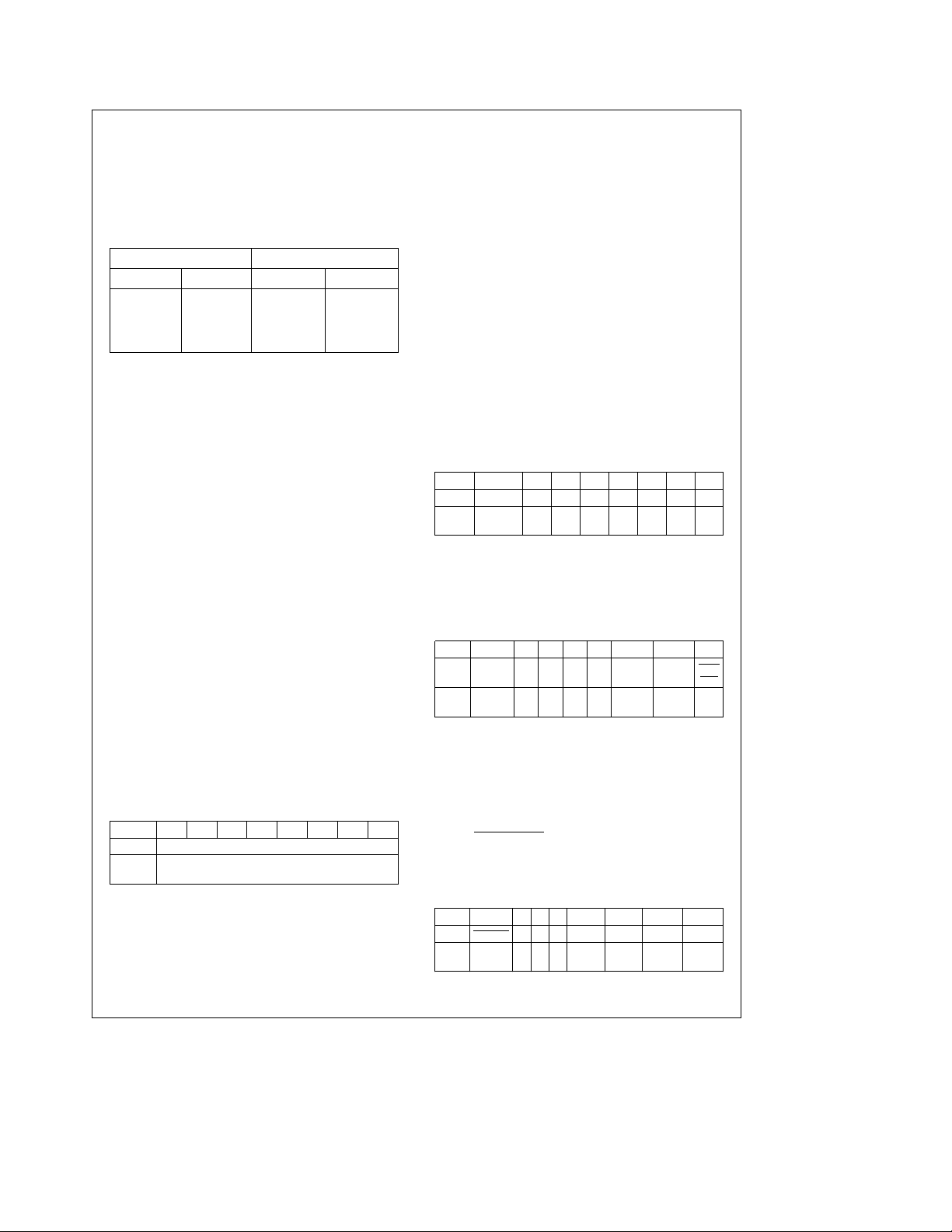
3.0 FDC Register Description (Continued)
D1,D0 Data Rate Select 1,0: These bits determine the
data rate for the floppy controller. See Table 3-6 for
the corresponding data rate for each value of D1,
D0. The data rate select bits are unaffected by a
software reset, and are set to 250 kb/s after a hardware reset.
TABLE 3-6. Data Rate Select Encoding
Data Rate Select Data Rate
1 0 MFM FM
1 1 1 Mb/s Illegal
0 0 500 kb/s 250 kb/s
0 1 300 kb/s 150 kb/s
1 0 250 kb/s 125 kb/s
Note: FM mode is not guaranteed through functional testing.
3.7 DATA REGISTER (FIFO) Read/Write
The FIFO (read/write) is used to transfer all commands,
data, and status between the mP and the FDC. During the
Command Phase, the mP writes the command bytes into the
FIFO after polling the RQM and DIO bits in the MSR. During
the Result Phase, the mP reads the result bytes from the
FIFO after polling the RQM and DIO bits in the MSR.
The enabling of the FIFO and setting of the FIFO threshold
is done via the Configure command. If the FIFO is enabled,
only the Execution Phase byte transfers use the 16 byte
FIFO. The FIFO is always disabled during the Command
and Result Phases of a controller operation. If the FIFO is
enabled, it will not be disabled after a software reset if the
LOCK bit is set in the Lock Command. After a hardware
reset, the FIFO is disabled to maintain compatibility with
PC-AT systems.
The 16-byte FIFO can be used for DMA, Interrupt, or software polling type transfers during the execution of a read,
write, format, or scan command. In addition, the FIFO can
be put into a Burst or Non-Burst mode with the Mode command. In the Burst mode, DRQ or IRQ6 remains active until
all of the bytes have been transferred to or from the FIFO. In
the Non-Burst mode, DRQ or IRQ6 is deasserted for 350 ns
to allow higher priority transfer requests to be serviced. The
Mode command can also disable the FIFO for either reads
or writes separately. The FIFO allows the system a larger
latency without causing a disk overrun/underrun error. Typical uses of the FIFO would be at the 1 Mb/s data rate, or
with multi-tasking operating systems. The default state of
the FIFO is disabled, with a threshold of zero. The default
state is entered after a hardware reset.
Data Register (FIFO)
D7 D6 D5 D4 D3 D2 D1 D0
Byte Mode
DRP
]
b
(16ct
ICP
)
DESC Data[7:0
RESET
COND
During the Execution Phase of a command involving data
transfer to/from the FIFO, the system must respond to a
data transfer service request based on the following formula:
Maximum Allowable Data Transfer Service Time
(THRESH
a
1)c8ct
This formula is good for all data rates with the FIFO enabled
or disabled. THRESH is a four bit value programmed in the
Configure command, which sets the FIFO threshold. If the
FIFO is disabled, THRESH is zero in the above formula. The
last term of the formula, (16
to the microcode overhead required by the FDC. This delay
is also data rate dependent. See Table 9-1 for the t
t
times.
ICP
c
t
) is an inherent delay due
ICP
DRP
and
The programmable FIFO threshold (THRESH) is useful in
adjusting the floppy controller to the speed of the system. In
other words, a slow system with a sluggish DMA transfer
capability would use a high value of THRESH, giving the
system more time to respond to a data transfer service request (DRQ for DMA mode or IRQ6 for Interrupt mode).
Conversely, a fast system with quick response to a data
transfer service request would use a low value of THRESH.
3.8 DIGITAL INPUT REGISTER (DIR) Read Only
This diagnostic register is used to detect the state of the
DSKCHG disk interface input and some diagnostic signals.
The function of this register depends on the register mode
of operation. When in the PC-AT mode, the D6 – D0 are
TRI-STATE to avoid conflict with the fixed disk status register at the same address. The DIR is unaffected by a software reset.
3.8.1 DIRÐPC-AT Mode
D7 D6 D5 D4 D3 D2 D1 D0
DESC DSKCHG XXXXXXX
RESET
COND
N/A N/A N/A N/A N/A N/A N/A N/A
D7 Disk Changed: Active high status of DSKCHG disk
interface input. During power down this bit will be
invalid, if it is read by the software.
D6–D0 Undefined: TRI-STATE. Used by Hard Disk Con-
troller Status Register.
3.8.2 DIRÐPS/2 Mode
D7 D6 D5 D4 D3 D2 D1 D0
DESC
DSKCHG 1 1 1 1 DRATE1 DRATE0
RESET
N/A N/A N/A N/A N/A N/A N/A 1
COND
1
HIGH
DEN
D7 Disk Changed: Active high status of DSKCHG disk
interface input. During power down this bit will be
invalid, if it is read by the software.
D6–D3 Reserved: Always 1.
D2,D1 Data Rate Select 1,0: These bits indicate the
status of the DRATE1,0 bits programmed through
the DSR CCR.
D0 High Density
: This bit is low when the 1 Mb/s or
500 kb/s data rate is chosen, and high when the
300 kb/s or 250 kb/s data rate is chosen. This bit is
independent of the IDENT value.
3.8.3 DIRÐModel 30 Mode
D7 D6 D5 D4 D3 D2 D1 D0
DESC DSKCHG 0 0 0 DMAEN NOPRE DRATE1 DRATE0
RESET
N/A 0 0 0 0 0 1 0
COND
22
Page 23
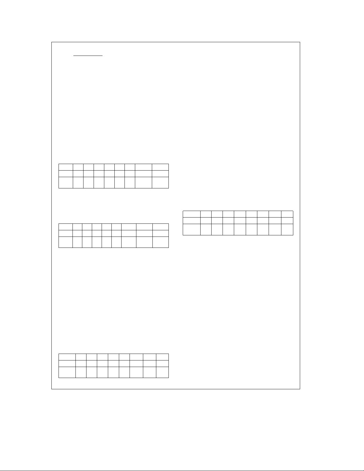
3.0 FDC Register Description (Continued)
D7 Disk Changed
interface input. During power down this bit will be
invalid, if it is read by the software.
D6–D4 Reserved: Always 0.
D3 DMA Enable: Active high status of the DMAEN bit
in the DOR.
D2 No Precompensation: Active high status of the
NOPRE bit in the CCR.
D1,D0 Data Rate Select 1,0: These bits indicate the
status of the DRATE 1,0 bits programmed through
the DSR/CCR.
3.9 CONFIGURATION CONTROL REGISTER (CCR)
Write Only
This is the write-only data rate register commonly used in
PC-AT applications. This register is not affected by a software reset, and is set to 250 kb/s after a hardware reset.
The data rate of the floppy controller is determined by the
last write to either the CCR or DSR.
3.9.1 CCRÐPC-AT and PS/2 Modes
D7 D6 D5 D4 D3 D2 D1 D0
DESC 000000DRATE1 DRATE0
RESET
N/A N/A N/A N/A N/A N/A 1 0
COND
D7–D2 Reserved: Should be set to 0.
D1,D0 Data Rate Select 1,0: These bits determine the
data rate of the floppy controller. See Table 3-6 for
the appropriate values.
3.9.2 CCRÐModel 30 Mode
D7 D6 D5 D4 D3 D2 D1 D0
DESC 0 0 0 0 0 NOPRE DRATE1 DRATE0
RESET
N/A N/A N/A N/A N/A N/A 1 0
COND
D7–D3 Reserved: Should be set to 0.
D2 No Precompensation: This bit can be set by soft-
ware, but it has no functionality. It can be read by bit
D2 of the DIR when in the Model 30 register mode.
Unaffected by a software reset.
D1,D0 Data Rate Select 1,0: These bits determine the
data rate of the floppy controller. See Table 3-6 for
the appropriate values.
3.10 RESULT PHASE STATUS REGISTERS
The Result Phase of a command contains bytes that hold
status information. The format of these bytes is described
below. Do not confuse these status bytes with the Main
Status Register, which is a read only register that is always
valid. The Result Phase status registers are read from the
Data Register (FIFO) only during the Result Phase of certain
commands (see Section 4.1 Command Set Summary). The
status of each register bit is indicated when the bit is a 1.
3.10.1 Status Register 0 (ST0)
D7 D6 D5 D4 D3 D2 D1 D0
DESC IC IC SE EC 0 HDS DS1 DS0
RESET
COND
00000 0 0 0
: Active low status of DSKCHG disk
D7–D6 Interrupt Code:
00eNormal Termination of Command.
01eAbnormal Termination of Command. Execu-
tion of command was started, but was not
successfully completed.
e
10
Invalid Command Issued. Command issued
was not recognized as a valid command.
e
11
Internal drive ready status changed state during the drive polling mode. Only occurs after a
hardware or software reset.
D5 Seek End: Seek, Relative Seek, or Recalibrate
command completed by the controller. (Used during
a Sense Interrupt command.)
D4 Equipment Check: After a Recalibrate command,
Track 0 signal failed to occur. (Used during Sense
Interrupt command.)
D3 Not Used. Always 0.
D2 Head Select: Indicates the active high status of the
HDSEL pin at the end of the Execution Phase.
D1,D0 Drive Select 1,0: These two binary encoded bits
indicate the logical drive selected at the end of the
Execution Phase.
e
00
Drive 0 selected.
01eDrive 1 selected.
10eDrive 2 selected.
e
Drive 3 selected.
11
3.10.2 Status Register 1 (ST1)
D7 D6 D5 D4 D3 D2 D1 D0
DESC ET 0 CE OR 0 ND NW MA
RESET
COND
000 00 0 0 0
D7 End of Track: Controller transferred the last byte of
the last sector without the TC pin becoming active.
The last sector is the End of Track sector number
programmed in the Command Phase.
D6 Not Used. Always 0.
D5 CRC Error: If this bit is set and bit 5 of ST2 is clear,
then there was a CRC error in the Address Field of
the correct sector. If bit 5 of ST2 is also set, then
there was a CRC error in the Data Field.
D4 Overrun: Controller was not serviced by the mP
soon enough during a data transfer in the Execution
Phase. For read operations, indicates a data overrun. For write operations, indicates a data underrun.
D3 Not Used. Always 0.
D2 No Data: Three possible problems:
1. Controller cannot find the sector specified in the
Command Phase during the execution of a Read,
Write, Scan, or Verify command. An address
mark was found however, so it is not a blank disk.
2. Controller cannot read any Address Fields without a CRC error during a Read ID command.
3. Controller cannot find starting sector during execution of Read A Track command.
D1 Not Writable: Write Protect pin is active when a
Write or Format command is issued.
23
Page 24
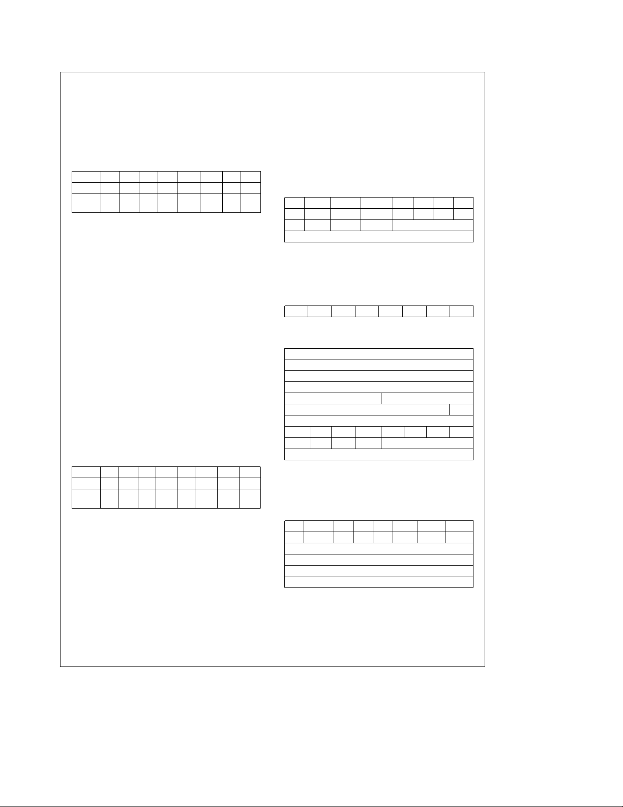
3.0 FDC Register Description
(Continued)
D0 Missing Address Mark: If bit 0 of ST2 is clear then
the controller cannot detect any Address Field Address Mark after two disk revolutions. If bit 0 of ST2
is set then the controller cannot detect the Data
Field Address Mark after finding the correct Address Field.
3.10.3 Status Register 2 (ST2)
D7 D6 D5 D4 D3 D2 D1 D0
DESC 0 CM CD WT SEH SNS BT MD
RESET
COND
D7 Not Used. Always 0.
D6 Control Mark: Controller tried to read a sector
D5 CRC Error in Data Field: Controller detected a
D4 Wrong Track: Only set if desired sector is not
D3 Scan Equal Hit: ‘‘Equal’’ condition satisfied during
D2 Scan Not Satisfied: Controller cannot find a sector
D1 Bad Track: Only set if the desired sector is not
D0 Missing Address Mark in Data Field: Controller
3.10.4 Status Register 3 (ST3)
DESC 0 WP 1 TK0 1 HDS DS1 DS0
RESET
COND
D7 Not Used. Always 0.
D6 Write Protect: Indicates active high status of the
D5 Not Used. Always 1.
D4 Track 0: Indicates active high status of the TRK0
D3 Not Used. Always 1.
D2 Head Select: Indicates the active high status of the
D1,D0 Drive Select 1,0: These two binary encoded bits
0000 0 0 00
which contained a deleted data address mark during execution of Read Data or Scan commands. Or,
if a Read Deleted Data command was executed, a
regular address mark was detected.
CRC error in the Data Field. Bit 5 of ST1 is also set.
found, and the track number recorded on any sector
of the current track is different from the track address specified in the Command Phase.
any Scan command.
on the track which meets the desired condition during any Scan command.
found, the track number recorded on any sector on
the track is FF (hex) indicating a hard error in IBM
format, and is different from the track address specified in the Command Phase.
cannot find the Data Field AM during a Read, Scan,
or Verify command. Bit 0 of ST1 is also set.
D7 D6 D5 D4 D3 D2 D1 D0
001010 0 0
WP pin.
pin.
HD bit in the Command Phase.
indicate the DS1,DS0 bits in the Command Phase.
4.0 FDC Command Set Description
The following is a table of the FDC command set. Each
command contains a unique first command byte called the
opcode byte which will identify to the controller how many
command bytes to expect. If an invalid command byte is
issued to the controller, it will immediately go into the Result
Phase and the status will be 80 (hex), which signifies Invalid
Command.
4.1 COMMAND SET SUMMARY
CONFIGURE
Command Phase
0 0 0 1 0011
0 0 0 0 0000
0 EIS FIFO POLL THRESH
PRETRK
Execution Phase: Internal registers written.
No Result Phase
DUMPREG
Command Phase
00001110
Execution Phase: Internal registers read.
Result Phase
PTR Drive 0
PTR Drive 1
PTR Drive 2
PTR Drive 3
Step Rate Time Motor Off Time
Motor On Time DMA
Sector per Track/End of Track
LOCK 0 DC3 DC2 DC1 DC0 GAP WG
0 EIS FIFO POLL THRESH
PRETRK
Note: Sectors per Track parameter returned if last command issued was
Format. End of Track parameter returned if last command issued was Read
or Write.
FORMAT TRACK
Command Phase
0 MFM 0 0 1 1 0 1
X X XXXHDDR1DR0
Bytes per Sector
Sectors per Track
Format Gap
Data Pattern
Execution Phase: System transfers four ID bytes (track,
head, sector, bytes/sector) per sector to the floppy controller via DMA or Non-DMA modes. The entire track is formatted. The data block in the Data Field of each sector is filled
with the data pattern byte.
24
Page 25

4.0 FDC Command Set Description (Continued)
Result Phase
Status Register 0
Status Register 1
Status Register 2
Undefined
Undefined
Undefined
Undefined
INVALID
Command Phase
Invalid Op Codes
Result Phase
Status Register 0 (80 hex)
LOCK
Command Phase
LOCK0010100
Execution Phase: Internal register is written.
Result Phase
000LOCK0000
MODE
Command Phase
0000 0 001
TMR IAF IPS 0 LOW PWR 1 ETR
FWR FRD BST R255 0 0 0 0
DENSEL BFR WLD Head Settle
0000 0RG0PU
Execution Phase: Internal registers are written.
No Result Phase
NSC
Command Phase
00011000
Result Phase
01110011
PERPENDICULAR MODE
Command Phase
000100 10
OW 0 DC3 DC2 DC1 DC0 GAP WG
Execution Phase: Internal registers are written.
No Result Phase
READ DATA
Command Phase
Execution Phase: Data read from disk drive is transferred
to system via DMA or Non-DMA modes.
Result Phase
READ DELETED DATA
Command Phase
Execution Phase: Data read from disk drive is transferred
to system via DMA or Non-DMA modes.
Result Phase
MT MFM SK 0 0 1 1 0
IPS X X X X HD DR1 DR0
Track Number
Drive Head Number
Sector Number
Bytes per Sector
End of Track Sector Number
Intersector Gap Length
Data Length
Status Register 0
Status Register 1
Status Register 2
Track Number
Head Number
Sector Number
Bytes per Sector
MT MFM SK 0 1 1 0 0
IPS X X X X HD DR1 DR0
Track Number
Drive Head Number
Sector Number
Bytes per Sector
End of Track Sector Number
Intersector Gap Length
Data Length
Status Register 0
Status Register 1
Status Register 2
Track Number
Head Number
Sector Number
Bytes per Sector
25
Page 26

4.0 FDC Command Set Description (Continued)
READ ID
Command Phase
0 MFM 0 0 1 0 1 0
X X XXXHDDR1DR0
Execution Phase: Controller reads first ID Field header
bytes it can find and reports these bytes to the system in the
result bytes.
Result Phase
Status Register 0
Status Register 1
Status Register 2
Track Number
Head Number
Sector Number
Bytes per Sector
READ A TRACK
Command Phase
0 MFM 0 0 0 0 1 0
IPS X X X X HD DR1 DR0
Track Number
Drive Head Number
Sector Number
Bytes per Sector
End of Track Sector Number
Intersector Gap Length
Data Length
Execution Phase: Data read from disk drive is transferred
to system via DMA or non-DMA modes.
Result Phase
Status Register 0
Status Register 1
Status Register 2
Track Number
Head Number
Sector Number
Bytes per Sector
RECALIBRATE
Command Phase
000001 1 1
000000DR1DR0
Execution Phase: Disk drive head is stepped out to Track
0.
No Result Phase
RELATIVE SEEK
Command Phase
Execution Phase: Disk drive head stepped in or out a pro-
grammable number of tracks.
No Result Phase
SCAN EQUAL
Command Phase
Execution Phase: Data transferred from system to control-
ler is compared to data read from disk.
Result Phase
SCAN HIGH OR EQUAL
Command Phase
Execution Phase: Data transferred from system to control-
ler is compared to data read from disk.
1 DIR 0 0 1 1 1 1
X X X X X HD DR1 DR0
Relative Track Number
MT MFM SK 1 0 0 0 1
IPS X X X X HD DR1 DR0
Track Number
Drive Head Number
Sector Number
Bytes per Sector
End of Track Sector Number
Intersector Gap Length
Sector Step Size
Status Register 0
Status Register 1
Status Register 2
Track Number
Head Number
Sector Number
Bytes per Sector
MT MFM SK 1 1 1 0 1
IPS X X X X HD DR1 DR0
Track Number
Drive Head Number
Sector Number
Bytes per Sector
End of Track Sector Number
Intersector Gap Length
Sector Step Size
26
Page 27

4.0 FDC Command Set Description (Continued)
Result Phase
Status Register 0
Status Register 1
Status Register 2
Track Number
Head Number
Sector Number
Bytes per Sector
SCAN LOW OR EQUAL
Command Phase
MT MFM SK 1 1 0 0 1
IPS X X X X HD DR1 DR0
Track Number
Drive Head Number
Sector Number
Bytes per Sector
End of Track Sector Number
Intersector Gap Length
Sector Step Size
Execution Phase: Data transferred from system to controller is compared to data read from disk.
Result Phase
Status Register 0
Status Register 1
Status Register 2
Track Number
Head Number
Sector Number
Bytes per Sector
SEEK
Command Phase
00001111
XXXXXHDDR1DR0
New Track Number
MSN of Track Number 0000
Note: Last Command Phase byte is required only if ETR is set in Mode
Command.
Execution Phase: Disk drive head is stepped in or out to a
programmable track.
No Result Phase
SENSE DRIVE STATUS
Command Phase
00000 1 0 0
XXXXXHDDR1DR0
Execution Phase: Disk drive status information is detected
and reported.
Result Phase
SENSE INTERRUPT
Command Phase
Execution Phase: Status of interrupt is reported.
Result Phase
Note: Third Result Phase byte can only be read if ETR is set in the Mode
Command.
SET TRACK
Command Phase
Execution Phase: Internal register is read or written.
Result Phase
SPECIFY
Command Phase
Execution Phase: Internal registers are written.
No Result Phase
VERIFY
Command Phase
Execution Phase: Data is read from disk but not transferred
to the system.
Status Register 3
00001000
Status Register 0
Present Track Number (PTR)
MSNofPTR 0000
0WNR100 0 0 1
0 0 1 1 0 MSB DR1 DR0
New Track Number (PTR)
Value
0000001 1
Step Rate Time Motor Off Time
Motor On Time DMA
MT MFM SK 1 0 1 1 0
EC X X X X HD DR1 DR0
Track Number
Drive Head Number
Sector Number
Bytes per Sector
End of Track Sector Number
Intersector Gap Length
Data Length/Sector Count
27
Page 28

4.0 FDC Command Set Description (Continued)
Result Phase
Status Register 0
Status Register 1
Status Register 2
Track Number
Head Number
Sector Number
Bytes per Sector
VERSION
Command Phase
00010000
Result Phase
10010000
WRITE DATA
Command Phase
MT MFM 0 0 0 1 0 1
IPS X X X X HD DR1 DR0
Track Number
Drive Head Number
Sector Number
Bytes per Sector
End of Track Sector Number
Intersector Gap Length
Data Length
Execution Phase: Data is transferred from the system to
the controller via DMA or Non-DMA modes and written to
the disk.
Result Phase
Status Register 0
Status Register 1
Status Register 2
Track Number
Head Number
Sector Number
Bytes per Sector
WRITE DELETED DATA
Command Phase
Execution Phase: Data is transferred from the system to
the controller via DMA or Non-DMA modes and written to
the disk.
Result Phase
4.2 COMMAND DESCRIPTION
4.2.1 Configure Command
The Configure Command will control some operation modes
of the controller. It should be issued during the initialization
of the FDC after power up. The function of the bits in the
Configure registers are described below. These bits are set
to their default values after a hardware reset. The value of
each bit after a software reset is explained. The default value of each bit is denoted by a ‘‘bullet’’ to the left of each
item.
EIS: Enable Implied Seeks. Default after a software reset.
#
MT MFM 0 0 1 0 0 1
IPS X X X X HD DR1 DR0
Track Number
Drive Head Number
Sector Number
Bytes per Sector
End of Track Sector Number
Intersector Gap Length
Data Length
Status Register 0
Status Register 1
Status Register 2
Track Number
Head Number
Sector Number
Bytes per Sector
0eImplied seeks disabled through Configure command.
Implied seeks can still be enabled through the Mode
command when EIS
e
Implied seeks enabled for a read, write, scan, or veri-
1
e
0. (default)
fy operation. A seek and sense interrupt operation
will be performed prior to the execution of the read,
write, scan, or verify operation. The IPS bit does not
need to be set.
28
Page 29

4.0 FDC Command Set Description (Continued)
FIFO: Enable FIFO for Execution Phase data transfers. De-
fault after a software reset if the LOCK bit is 0. If the LOCK
bit is 1, then the FIFO bit will retain its previous value after a
software reset.
e
0
FIFO enabled for both reads and writes.
1eFIFO disabled. (default)
#
POLL: Disable for Drive Polling Mode. Default after a software reset.
0eEnable polling mode. An interrupt is generated after a
#
reset. (default)
e
1
Disable drive polling mode. If the Configure command
is issued within 500 ms of a hardware or software reset,
then an interrupt will not be generated. In addition, the
four Sense Interrupt commands to clear the ‘‘Ready
Changed State’’ of the four logical drives will not be
required.
THRESH: The FIFO threshold in the Execution Phase of
read and write data transfers. Programmable from 00 to 0F
hex. Defaults to 00 after a software reset if the LOCK bit is
0. If the LOCK bit is 1, then THRESH will retain its value. A
high value of THRESH is suited for slow response systems,
and a low value of THRESH is better for fast response systems.
PRETRK: Starting track number for write precompensation.
Programmable from track 0 (‘‘00’’) to track 255 (‘‘FF’’). Defaults to track 0 (‘‘00’’) after a software reset if the LOCK bit
is 0. If the LOCK bit is 1, then PRETRK will retain its value.
4.2.2 Dumpreg Command
The Dumpreg command is designed to support system runtime diagnostics and application software development and
debug. This command has a one byte command phase and
a ten byte result phase, which return the values of parameters set in other commands. That is, the PTR (Present Track
Register) contains the least significant byte of the track the
microcode has stored for each drive. The Step Rate Time,
Motor Off and Motor On Times, and the DMA bit are all set
in the Specify command.
The sixth byte of the result phase varies depending on what
commands have been previously executed.
If a format command has previously been issued, and no
reads or writes have been issued since then, this byte will
contain the sectors per track value. If a read or write command has been executed more recently than a format command, this byte will contain the end of track value. The
LOCK bit is set in the Lock command. The eighth result byte
also contains the bits programmed in the Perpendicular
Mode command. The last two bytes of the Dumpreg Result
Phase are set in the Configure command. After a hardware
or software reset, the parameters in the result bytes will be
set to their appropriate default values.
Note: Some of these parameters are unaffected by a software reset, de-
4.2.3 Format Track Command
This command will format one track on the disk in IBM, ISO,
or Perpendicular Format. After the index hole is detected,
data patterns are written on the disk including all gaps, address marks, Address Fields, and Data Fields. The exact
format is determined by the following parameters:
1. The MFM bit in the Opcode (first command) byte, which
2. The IAF bit in the Mode command, which selects be-
3. The WGATE and GAP bits in the Perpendicular Mode
4. The Bytes per Sector code, which determines the sector
5. The Sector per Track parameter, which determines how
6. The Data Pattern byte, which is used as the filler byte in
pending on the state of the LOCK bit.
determines the format of the Address Marks and the encoding scheme.
tween IBM and ISO format.
command, which select between the conventional and
Toshiba Perpendicular format.
size.
many sectors will be formatted on the track.
the Data Field of each sector.
29
Page 30

4.0 FDC Command Set Description (Continued)
To allow for flexible formatting, the mP must supply the four
Address Field bytes (track, head, sector, bytes per sector
code) for each sector formatted during the Execution
Phase. This allows for non-sequential sector interleaving.
This transfer of bytes from the mP to the controller can be
done in the DMA or Non-DMA mode, with the FIFO enabled
or disabled.
The Format command terminates when the index hole is
detected a second time, at which point an interrupt is generated. Only the first three status bytes in the Result Phase
are significant. The Format Gap byte in the Command
Phase is dependent on the data rate and type of disk drive,
and will control the length of GAP3. Some typical values for
the programmable GAP3 are given in Table 4-1 (next page).
Figure 4-1
formats supported by the floppy controller.
shows the track format for the three types of
Notes:
e
Data Pattern of FE, Clock Pattern of C7
FE*
e
FC*
Data Pattern of FC, Clock Pattern of D7
e
FB*
Data Pattern of FB, Clock Pattern of C7
e
F8*
Data Pattern of F8, Clock Pattern of C7
e
A1*
Data Pattern of A1, Clock Pattern of 0A
e
C2*
Data Pattern of C2, Clock Pattern of 14
FIGURE 4-1. IBM, Perpendicular, and ISO Formats Supported by Format Command
All byte counts in decimal
All byte values in hex
CRC uses standard polynomial x
Perpendicular Format GAP2
All other data rates use GAP2
FM mode is not guaranteed through functional testing.
16
a
e
41 bytes for 1 Mb/s.
e
22 bytes
30
TL/F/11362– 5
12
5
a
a
x
x
1
Page 31

4.0 FDC Command Set Description (Continued)
TABLE 4-1. Typical Format Gap Length Values
Mode
Sector Sector
Size Code Gap GAP3
EOT
Decimal Hex Hex Hex Hex
125 kb/s 128 00 12 07 09
FM 128 00 10 10 19
256 01 08 18 30
512 02 04 46 87
1024 03 02 C8 FF
2048 04 01 C8 FF
250 kb/s 256 01 12 0A 0C
MFM 256 01 10 20 32
512 02 08 2A 50
512 02 09 2A 50
1024 03 04 80 F0
2048 04 02 C8 FF
4096 05 01 C8 FF
250 kb/s 128 00 1A 07 1B
FM 256 01 0F 0E 2A
512 02 08 1B 3A
1024 03 04 47 8A
2048 04 02 C8 FF
4096 05 01 C8 FF
500 kb/s 256 01 1A 0E 36
MFM 512 02 0F 1B 54
512 02 12 1B 6C
1024 03 08 35 74
2048 04 04 99 FF
4096 05 02 C8 FF
8192 06 01 C8 FF
Note: FM mode is not guaranteed through functional testing.
Typical Values for PC Compatible Diskette Media
Media Sector Sector
Type Size Code Gap GAP3
EOT
Decimal Hex Hex Hex Hex
360k 512 02 09 2A 50
1.2M 512 02 0F 1B 54
720k 512 02 09 1B 50
1.44M 512 02 12 1B 6C
2.88M 512 02 24 1B 53
Note 1: Sector Gap refers to the Intersector Gap Length parameter specified in the Command Phase of the Read, Write, Scan, and Verify commands. Although this
is the recommended value, the FDC treats this byte as a don’t care in the Read, Write, Scan, and Verify commands.
Note 2: Format Gap is the suggested value to use in the Format Gap parameter of the Format command. This is the programmable GAP3 as shown in
Note 3: The 2.88M diskette media is a Barium Ferrite media intended for use in Perpendicular Recording drives at the data rate of up to 1 Mb/s.
Sector Format
Sector Format
Figure 4-1
.
31
Page 32

4.0 FDC Command Set Description (Continued)
4.2.4 Invalid Command
If an invalid command (Illegal Opcode byte in the Command
Phase) is received by the controller, the controller will respond with ST0 in the Result Phase. The controller does not
generate an interrupt during this condition. Bits 6 and 7 in
the MSR are both set to a 1, indicating to the mP that the
controller is in the Result Phase and the contents of ST0
must be read. The system will read an 80 (hex) value from
ST0, indicating an invalid command was received.
4.2.5 Lock Command
The Lock command allows the user full control of the FIFO
parameters after a software reset. If the LOCK bit is set to 1,
then the FIFO, THRESH, and PRETRK bits in the Configure
command are not affected by a software reset. In addition,
the FWR, FRD, and BST bits in the Mode command will be
unaffected by a software reset. If the LOCK is 0 (default
after a hardware reset), then the above bits will be set to
their default values after a software reset. This command is
useful if the system designer wishes to keep the FIFO enabled and retain the other FIFO parameter values (such as
THRESH) after a software reset.
After the command byte is written, the result byte must be
read before continuing to the next command. The execution
of the Lock command is not performed until the result byte
is read by the mP. If the part is reset after the command byte
is written but before the result byte is read, then the Lock
command execution will not be performed. This is done to
prevent accidental execution of the Lock command.
4.2.6 Mode Command
This command is used to select the special features of the
controller. The bits for the Command Phase bytes are
shown in Section 4.1, Command Set Summary, and their
function is described below. These bits are set to their default values after a hardware reset. The default value of
each bit is denoted by a ‘‘bullet’’ to the left of each item. The
value of each parameter after a software reset will be explained.
TMR: Motor Timer mode. Default after a software reset.
0eTimers for motor on and motor off are defined for
#
Mode 1. (See Specify command.) (default)
e
1
Timers for motor on and motor off are defined for
Mode 2. (See Specify command.)
IAF: Index Address Format. Default after a software reset.
0eThe controller will format tracks with the Index Ad-
#
dress Field included. (IBM and Perpendicular format.)
e
1
The controller will format tracks without including the
Index Address Field. (ISO format.)
IPS: Implied Seek. Default after a software reset.
0eThe implied seek bit in the command byte of a read,
#
write, scan, or verify is ignored. Implied seeks could
still be enabled by the EIS bit in the Configure command.
e
1
The IPS bit in the command byte of a read, write,
scan, or verify is enabled so that if it is set, the controller will perform seek and sense interrupt operations before executing the command.
LOW PWR: Low Power mode. Default after a software reset.
#
ETR: Extended Track Range. Default after a software reset.
#
FWR: FIFO Write Disable for mP write transfers to control-
ler. Default after a software reset if LOCK is 0. If LOCK is 1,
FWR will retain its value after a software reset.
Note: This bit is only valid if the FIFO is enabled in the Configure command.
#
FRD: FIFO Read Disable for mP read transfers from control-
ler. Default after a software reset if LOCK is 0. If LOCK is 1,
FRD will retain its value after a software reset.
Note: This bit is only valid if the FIFO is enabled in the Configure command.
#
BST: Burst Mode Disable. Default after a software reset if
LOCK is 0. If LOCK is 1, BST will retain its value after a
software reset.
Note: This bit is only valid if the FIFO is enabled in the Configure command.
#
00eCompletely disable the low power mode. (default)
e
Automatic low power. Go into low power mode
01
512 ms after the head unload timer times out. (This
assumes a 500 kb/s data rate.) For 250 kb/s the
timeout period is doubled to 1 ms.
e
10
Manual low power. Go into low power mode now.
11eNot used.
0eTrack number is stored as a standard 8-bit value
compatible with the IBM, ISO, and Perpendicular formats. This will allow access of up to 256 tracks during a seek operation.
e
1
Track number is stored as a 12-bit value. The upper
four bits of the track value are stored in the upper
four bits of the head number in the sector Address
Field. This allows access of up to 4096 tracks during
a seek operation. With this bit set, an extra byte is
required in the Seek Command Phase and Sense Interrupt Result Phase.
If the FIFO is not enabled in the Configure command, then this bit is a
don’t care.
0eEnable FIFO. Execution Phase mP write transfers use
the internal FIFO. (default)
e
1
Disable FIFO. All write data transfers take place without the FIFO.
If the FIFO is not enabled in the Configure command, then this bit is a
don’t care.
0eEnable FIFO. Execution Phase mP read transfers use
the internal FIFO. (default)
e
1
Disable FIFO. All read data transfers take place without the FIFO.
If the FIFO is not enabled in the Configure command, then this bit is a
don’t care.
0eBurst mode enabled for FIFO Execution Phase data
transfers. (default)
e
1
Non-Burst mode enabled. The DRQ or IRQ6 pin will
be strobed once for each byte to be transferred while
the FIFO is enabled.
32
Page 33

4.0 FDC Command Set Description (Continued)
R255: Recalibrate Step Pulses. The bit will determine the
maximum number of recalibrate step pulses the controller
will issue before terminating with an error. Default after a
software reset.
0e85 maximum recalibrate step pulses. If ETRe1,
#
controller will issue 3925 recalibrate step pulses maximum.
e
1
255 maximum recalibrate step pulses. If ETRe1,
controller will issue 4095 maximum recalibrate step
pulses.
DENSEL: Density Select Pin Configuration. This two bit value will configure the Density Select output to one of three
possible modes. The default mode will configure the
DENSEL pin according to the state of the IDENT input pin
after a data rate has been selected. That is, if IDENT is high,
the DENSEL pin is active high for the 500 kbs/1 Mbs data
rates. If IDENT is low, the DENSEL pin is active low for the
500 kbs/1 Mbs data rates. In addition to these modes, the
DENSEL output can be set to always low or always high, as
shown in Table 4-2. This will allow the user more flexibility
with new drive types.
TABLE 4-2. DENSEL Encoding
Bit 1 Bit 0
0 0 Pin Low
0 1 Pin High
1 0 Undefined
1 1 DEFAULT
TABLE 4-3. DENSEL Default Encoding
Data Rate
250 kb/s Low High
300 kb/s Low High
500 kb/s High Low
1 Mb/s High Low
BFR: CMOS Disk Interface Buffer Enable.
0eDrive output signals configured as standard 4 mA
#
push-pull outputs (actually 40 mA sink, 4 mA source).
(default)
e
1
Drive output signals configured as 40 mA open-drain
outputs.
WLD: Scan Wild Card.
0eAn FF (hex) from either the mP or the disk during a
#
Scan command is interpreted as a wildcard character
that will always match true. (default)
e
1
The Scan commands do not recognize FF (hex) as a
wildcard character.
Head Settle: Time allowed for read/write head to settle after a seek during an Implied Seek operation. This is controlled as shown in table in next column, by loading a 4-bit
value for N (the default value for N is 8).
DENSEL (default)
IDENTe1 IDENTe0
DENSEL
Pin Definition
RG: Read Gate Diagnostic.
#
PU: PUMP Pulse Output Diagnostic.
#
4.2.7 NSC Command
The NSC command can be used to distinguish between the
FDC versions and the 82077. The Result Phase byte
uniquely identifies the floppy controller as a PC87311A/12,
which returns a value of 72h. The 82077 and DP8473 return
a value of 80h, signifying an invalid command. The lower
four bits of this result byte are subject to change by NSC,
and will reflect the particular version of the floppy disk controller part.
4.2.8 Perpendicular Mode Command
The Perpendicular Mode command is designed to support
the unique Format and Write Data requirements of Perpendicular (Vertical) Recording disk drives (4 Mbytes unformatted capacity). The Perpendicular Mode command will configure each of the four logical drives as a perpendicular or
conventional disk drive. Configuration of the four logical disk
drives is done via the D3 – D0 bits, or with the GAP and WG
control bits. This command should be issued during the initialization of the floppy controller.
Perpendicular Recording drives operate in ‘‘Extra High Density’’ mode at 1 Mb/s, and are downward compatible with
1.44 Mbyte and 720 kbyte drives at 500 kb/s (High Density)
and 250 kb/s (Double Density) respectively. If perpendicular
drives are present in the system, this command should be
issued during initialization of the floppy controller, which will
configure each drive as perpendicular or conventional.
Then, when a drive is accessed for a Format or Write Data
command, the floppy controller will adjust the Format or
Write Data parameters based on the data rate (see Table
4-4).
Data Rate Multiplier Head Settle
kbits/s 4 Bits Time (ms)
250 Nc8 0– 120
300 N
500 N
1000 N
0eEnable DSKCHG disk interface input for normal oper-
ation. (default)
e
1
Enable DSKCHG to act as an external Read Gate
input signal to the Data Separator. This is intended as
a test mode to aid in evaluation of the Data Separator.
0eEnable MFM output pin for normal operation.
(default)
e
1
Enable the MFM output to act as the active low output of the Data Separator charge pump. This signal
consists of a series of pulses indicating when the
phase comparator is making a phase correction. This
Pump output will be active low for a pump up or pump
down signal from the phase comparator, and is intended as a test mode to aid in the evaluation of the
Data Separator.
c
6.666 0 –100
c
4 0–60
c
2 0–30
33
Page 34

4.0 FDC Command Set Description (Continued)
Looking at the second command byte, DC3 –DC0 correspond to the four logical drives. A 0 written to DCn sets
drive n to conventional mode, and a 1 sets drive n to perpendicular mode. Also, the OW (Overwrite) bit offers additional control. When OW
DC0 (drive configuration bits) is enabled. When OW
e
1, changing the values of DC3 –
e
the internal values of DC3 – DC0 are unaffected, regardless
of what is written to DC3–DC0.
The function of the DCn bits must also be qualified by setting both WG and GAP to 0. If WG and GAP are used (i.e.,
not set to 00), they will override whatever is programmed in
the DCn bits. Table 4-4a below indicates the operation of
the FDC based on the values of GAP and WG. Note that
when GAP and WG are both 0, the DCn bits are used to
configure each logical drive as conventional or perpendicular. DC3 –DC0 are unaffected by a software reset, but WG
and GAP are both cleared to 0 after a software reset. A
hardware reset will reset all the bits to zero (conventional
mode for all drives). The Perpendicular Mode command bits
may be rewritten at any time.
Note: When in the Perpendicular Mode for any drive at any data rate select-
ed by the DC0 –3 bits, write precompensation is set to zero.
Perpendicular Recording type disk drives have a Pre-Erase
Head which leads the Read/Write Head by 200 mm, which
translates to 38 bytes at the 1 Mb/s data transfer rate (19
bytes at 500 kb/s). The increased spacing between the two
heads requires a larger GAP2 between the Address Field
and Data Field of a sector at 1 Mb/s. (See Perpendicular
Format in Table 4-1.) This GAP2 length of 41 bytes (at
1 Mb/s) will ensure that the Preamble in the Data Field is
completely ‘‘pre-erased’’ by the Pre-Erase Head. Also, during Write Data operations to a perpendicular drive, a portion
of GAP2 must be rewritten by the controller to guarantee
that the Data Field Preamble has been pre-erased (see
Table 4-4).
4.2.9 Read Data Command
The Read Data command reads logical sectors containing a
Normal Data AM from the selected drive and makes the
data available to the host mP. After the last Command
Phase byte is written, the controller will simulate the Motor
0,
On time for the selected drive internally. The user must turn
on the drive motor directly by enabling the appropriate drive
and motor select disk interface outputs with the Digital Output Register (DOR).
If Implied Seeks are enabled, the controller will perform a
Seek operation to the track number specified in the Command Phase. The controller will also issue a Sense Interrupt
for the seek and wait the Head Settle time specified in the
Mode command.
The correct ID information (track, head, sector, bytes per
sector) for the desired sector must be specified in the command bytes. See Table 4-5 Sector Size Selection for details
on the bytes per sector code. In addition, the End of Track
Sector Number (EOT) should be specified, allowing the controller to read multiple sectors. The Data Length byte is a
don’t care and should be set to FF (hex).
TABLE 4-5. Sector Size Selection
Bytes per Number of Bytes
Sector Code in Data Field
0 128
1 256
2 512
3 1024
4 2048
5 4096
6 8192
7 16384
TABLE 4-4. Effect of Drive Mode and Data Rate on Format and Write Commands
Data Rate
Drive
Mode
GAP2 Length Portion of GAP2
Written during Re-Written by Write
Format Data Command
250/300/500 kb/s Conventional 22 Bytes 0 Bytes
Perpendicular 22 Bytes 19 Bytes
1 Mb/s Conventional 22 Bytes 0 Bytes
Perpendicular 41 Bytes 38 Bytes
TABLE 4-4a. Effect of GAP and WG on Format and Write Commands
GAP WG
Mode
Description
GAP2 Length Portion of GAP2
Written during Re-Written by Write
Format Data Command
0 0 Conventional 22 Bytes 0 Bytes
0 1 Perpendicular 22 Bytes 19 Bytes
s
(
500 kb/s)
1 0 Reserved 22 Bytes 0 Bytes
(Conventional)
1 1 Perpendicular 41 Bytes 38 Bytes
(1 Mb/s)
34
Page 35

4.0 FDC Command Set Description (Continued)
The controller then starts the Data Separator and waits for
the Data Separator to find the next sector Address Field.
The controller compares the Address Field ID information
(track, head, sector, bytes per sector) with the desired ID
specified in the Command Phase. If the sector ID bytes do
not match, then the controller waits for the Data Separator
to find the next sector Address Field. The ID comparison
process repeats until the Data Separator finds a sector Address Field ID that matches it in the command bytes, or until
an error occurs. Possible errors are:
1. The mP aborted the command by writing to the FIFO. If
there is no disk in the drive, the controller will hang up.
The mP must then take the controller out of this hung
state by writing a byte to the FIFO. This will put the controller into the Result Phase.
2. Two index pulses were detected since the search began,
and no valid ID has been found. If the track address ID
differs, the WT bit or BT bit (if the track address is FF hex)
will be set in ST2. If the head, sector, or bytes per sector
code did not match, the ND bit is set in ST1. If the Address Field AM was never found, the MA bit is set in ST1.
3. The Address Field was found with a CRC error. The CE
bit is set in ST1.
Once the desired sector Address Field is found, the controller waits for the Data Separator to find the subsequent Data
Field for that sector. If the Data Field (normal or deleted) is
not found within the expected time, the controller terminates
the operation and enters the Result Phase (MD is set in
ST2). If a Deleted Data Mark is found and SK was set in the
Opcode command byte, the controller skips this sector and
searches for the next sector Address Field as described
above. The effect of SK on the Read Data command is
summarized in Table 4-6.
TABLE 4-6. SK Effect on Read Data Command
SK Data Type Sector Read ? CM Bit (ST2) Description of Results
0 Normal Y 0 Normal Termination
0 Deleted Y 1 No Further Sectors Read
1 Normal Y 0 Normal Termination
1 Deleted N 1 Sector Skipped
Having found the Data Field, the controller then transfers
data bytes from the disk drive to the host (described in Section 5.3 Controller Phases) until the bytes per sector count
has been reached, or the host terminates the operation
(through TC, end of track, or implicitly through overrun). The
controller will then generate the CRC for the sector and
compares this value with the CRC at the end of the Data
Field.
Having finished reading the sector, the controller will continue reading the next logical sector unless one or more of the
following termination conditions occurred:
1. The DMA controller asserted TC. The IC bits in ST0 are
set to Normal Termination.
2. The last sector address (of side 1 if MT was set) was
equal to EOT. The EOT bit in ST1 is set. The IC bits in
ST0 are set to Abnormal Termination. This is the expected condition during Non-DMA transfers.
3. Overrun error. The OR bit in ST1 is set. The IC bits in ST0
are set to Abnormal Termination. If the mP cannot service
a transfer request in time, the last correctly read byte will
be transferred.
4. CRC error. The CE bit in ST1 and CD bit in ST2 are set.
The IC bits in ST0 are set to Abnormal Termination.
If MT was set in the Opcode command byte, and the last
sector of side 0 has been transferred, the controller will then
continue with side 1.
Upon terminating the Execution Phase of the Read Data
command, the controller will assert IRQ6, indicating the beginning of the Result Phase. The mP must then read the
result bytes from the FIFO. The values that will be read back
in the result bytes are shown in Table 4-7. If an error occurs,
the result bytes will indicate the sector read when the error
occurred.
TABLE 4-7. Result Phase Termination Values with No Error
MT HD
00
00
01
01
10
10
11
11
EOTeEnd of Track Sector Number from Command Phase SeSector Number last operated on by controller
e
NC
No Change in Value TeTrack Number programmed in Command Phase
Last
Sector
k
EOT NC NC Sa1NC
e
EOT Ta1NC 1 NC
k
EOT NC NC Sa1NC
e
EOT Ta1NC 1 NC
k
EOT NC NC Sa1NC
e
EOT NC 1 1 NC
k
EOT NC NC Sa1NC
e
EOT Ta10 1 NC
Track Head Sector Bytes/Sector
ID Information at Result Phase
35
Page 36

4.0 FDC Command Set Description (Continued)
4.2.10 Read Deleted Data Command
The Read Deleted Data command reads logical sectors
containing a Deleted Data AM from the selected drive and
makes the data available to the host mP. This command is
identical to the Read Data command, except for the setting
of the CM bit in ST2 and the skipping of sectors. The effect
of SK on the Read Deleted Data command is summarized in
Table 4-8. See Table 4-7 for the state of the result bytes for
a Normal Termination of the command.
4.2.11 Read ID Command
The Read ID command finds the next available Address
Field and returns the ID bytes (track, head, sector, bytes per
sector) to the mP in the Result Phase. There is no data
transfer during the Execution Phase of this command. An
interrupt will be generated when the Execution Phase is
completed.
The controller first simulates the Motor On time for the selected drive internally. The user must turn on the drive motor
directly by enabling the appropriate drive and motor select
disk interface outputs with the Digital Output Register
(DOR). The Read ID command does not perform an implied
seek.
After waiting the Motor On time, the controller starts the
Data Separator and waits for the Data Separator to find the
next sector Address Field. If an error condition occurs, the
IC bits in ST0 are set to Abnormal Termination, and the
controller enters the Result Phase. Possible errors are:
1. The mP aborted the command by writing to the FIFO. If
there is no disk in the drive, the controller will hang up.
The mP must then take the controller out of this hung
state by writing a byte to the FIFO. This will put the controller into the Result Phase.
2. Two index pulses were detected since the search began,
and no AM has been found. If the Address Field AM was
never found, the MA bit is set in ST1.
4.2.12 Read A Track Command
The Read A Track command reads sectors in physical order
from the selected drive and makes the data available to the
host. This command is similar to the Read Data command
except for the following differences:
1. The controller waits for the index pulse before searching
for a sector Address Field. If the mP writes to the FIFO
before the index pulse, the command will enter the Result
Phase with the IC bits in ST0 set to Abnormal Termination.
2. A comparison of the sector Address Field ID bytes will be
performed, except for the sector number. The internal
sector address is set to 1, and then incremented for each
successive sector read.
TABLE 4-8. SK Effect on Read Deleted Data Command
SK Data Type Sector Read ? CM Bit (ST2) Description of Results
0 Normal Y 1 No Further Sectors Read
0 Deleted Y 0 Normal Termination
1 Normal N 1 Sector Skipped
1 Deleted Y 0 Normal Termination
3. If the Address Field ID comparison fails, the controller
sets ND in ST1, but continues to read the sector. If there
is a CRC error in the Address Field, the controller sets CE
in ST1, but continues to read the sector.
4. Multi-track and Skip operations are not allowed. SK and
MT should be set to 0.
5. If there is a CRC error in the Data Field, the controller
sets CE in ST1 and CD in ST2, but continues reading
sectors.
6. The controller reads a maximum of EOT physical sectors.
There is no support for multi-track reads.
4.2.13 Recalibrate Command
The Recalibrate command is very similar to the Seek command. The controller sets the Present Track Register (PTR)
of the selected drive to zero. It then steps the head of the
selected drive out until the TRK0 disk interface input signal
goes active, or until the maximum number of step pulses
have been issued. See Table 4-9 for the maximum recalibrate step pulse values based on the R255 and ETR bits in
the Mode command. If the number of tracks on the disk
drive exceeds the maximum number of recalibrate step
pulses, another Recalibrate command may need to be issued.
TABLE 4-9. Maximum Recalibrate Step Pulses
R255 ETR
0 0 85 (default)
1 0 255
0 1 3925
1 1 4095
After the last command byte is issued, the DRx BUSY bit is
set in the MSR for the selected drive. The controller will
simulate the Motor On time, and then enter the Idle Phase.
The execution of the actual step pulses occurs while the
controller is in the Drive Polling Phase. An interrupt will be
generated after the TRK0 signal is asserted, or after the
maximum number of recalibrate step pulses are issued.
There is no Result Phase. Recalibrates on more than one
drive at a time should not be issued for the same reason as
explained in the Seek command. No other command except
the Sense Interrupt command should be issued while a Recalibrate command is in progress.
4.2.14 Relative Seek Command
The Relative Seek command steps the selected drive in or
out a given number of steps. This command will step the
read/write head an incremental number of tracks, as op-
Based on R255 and ETR
Maximum Recalibrate
Step Pulses
36
Page 37

4.0 FDC Command Set Description (Continued)
posed to comparing against the internal present track register for that drive. The Relative Seek parameters are defined
as follows:
DIR: Read/Write Head Step Direction Control
e
0
Step Head Out
e
Step Head In
1
RTN: Relative Track Number. This value will determine how
many incremental tracks to step the head in or out from the
current track number.
The controller will issue RTN number of step pulses and
update the Present Track Register for the selected drive.
The one exception to this is if the TRK0 disk input goes
active, which indicates that the drive read/write head is at
the outermost track. In this case, the step pulses for the
Relative Seek are terminated, and the PTR value is set according to the actual number of step pulses issued. The
arithmetic is done modulo 255. The DRx BUSY bit in the
MSR is set for the selected drive. The controller will simulate the Motor On time before issuing the step pulses. After
the Motor On time, the controller will enter the Idle Phase.
The execution of the actual step pulses occurs in the Idle
Phase of the controller.
After the step operation is complete, the controller will generate an interrupt. There is no Result Phase. Relative Seeks
on more than one drive at a time should not be issued for
the same reason as explained in the Seek command. No
other command except the Sense Interrupt command
should be issued while a Relative Seek command is in progress.
4.2.15 Scan Commands
The Scan command allows data read from the disk to be
compared against data sent from the mP. There are three
Scan commands to choose from:
Scan Equal Disk Data
e
mP Data
Scan Low or Equal Disk DatasmP Data
Scan High or Equal Disk DatatmP Data
Each sector is interpreted with the most significant bytes
first. If the Wildcard mode is enabled in the Mode command,
an FF (hex) from either the disk or the mP is used as a don’t
care byte that will always match equal. After each sector is
read, if the desired condition has not been met, the next
sector is read. The next sector is defined as the current
sector number plus the Sector Step Size specified. The
Scan command will continue until the scan condition has
been met, or the EOT has been reached, or if TC is asserted.
Read errors on the disk will have the same error conditions
as the Read Data command. If the SK bit is set, sectors with
deleted data marks are ignored. If all sectors read are
skipped, the command will terminate with D3 of ST2 set
(Scan Equal Hit). The Result Phase of the command is
shown in Table 4-10.
4.2.16 Seek Command
The Seek command issues step pulses to the selected drive
in or out until the desired track number is reached. During
the Execution Phase of the Seek command, the track number to seek to is compared with the present track number.
The controller will determine how many step pulses to issue
and the DIR disk interface output will indicate which direction the R/W head should move. The DRx BUSY bit is set in
the MSR for the appropriate drive. The controller will wait
the Motor On time before issuing the first step pulse.
After the Motor On time, the controller will enter the Idle
Phase. The execution of the actual step pulses occurs in the
Drive Polling phase of the controller. The step pulse rate is
determined by the value programmed in the Specify command. An interrupt will be generated one step pulse period
after the last step pulse is issued. There is no Result Phase.
A Sense Interrupt command should be issued to determine
the cause of the interrupt.
While the internal microengine is capable of multiple seek
on 2 or more drives at the same time, software should ensure that only one drive is seeking or recalibrating at a time.
This is because the drives are actually selected via the
DOR, which can only select one drive at a time. No other
command except a Sense Interrupt command should be issued while a Seek command is in progress.
If the extended track range mode is enabled with the ETR
bit in the Mode command, a fourth command byte should be
written in the Command Phase to indicate the four most
significant bits of the desired track number. Otherwise, only
three command bytes should be written.
4.2.17 Sense Drive Status Command
The Sense Drive Status command returns the status of the
selected disk drive in ST3. This command does not generate an interrupt.
4.2.18 Sense Interrupt Command
The Sense Interrupt command is used to determine the
cause of interrupt when the interrupt is a result of the
TABLE 4-10. Scan Command Termination Values
Status
Command Register 2 Conditions
D2 D3
Scan Equal 0 1 DiskemP
1 0 Disk
i
mP
Scan Low 0 1 DiskemP
or Equal 0 0 DiskkmP
1 0 Disk
l
mP
Scan High 0 1 DiskemP
or Equal 0 0 Disk
1 0 Disk
l
mP
k
mP
37
Page 38

4.0 FDC Command Set Description (Continued)
change in status of any disk drive. Four possible causes of
the interrupt are:
1. Upon entering the Result Phase of:
a. Read Data command
b. Read Deleted Data command
c. Read a Track command
d. Read ID command
e. Write Data command
f. Write Deleted Data command
g. Format command
h. Scan command
i. Verify command
2. During data transfers in the Execution Phase while in the
Non-DMA mode.
3. Ready Changed State during the polling mode for an internally selected drive. (Occurs only after a hardware or
software reset.)
4. Seek, Relative Seek, or Recalibrate termination.
An interrupt due to reasons 1 and 2 does not require the
Sense Interrupt command and is cleared automatically. This
interrupt occurs during normal command operations and is
easily discernible by the mP via the MSR. This interrupt is
cleared reading or writing information from/to the Data Register (FIFO).
Interrupts caused by reasons 3 and 4 are identified with the
aid of the Sense Interrupt command. The interrupt is cleared
after the first result byte has been read. Use bits 5, 6, and 7
of ST0 to identify the cause of the interrupt as shown in
Table 4-11.
TABLE 4-11. Status Register 0 Termination Codes
Status Register 0
Interrupt Seek
Code End
D7 D6 D5
1 1 0 Internal Ready Went True
0 0 1 Normal Seek Termination
0 1 1 Abnormal Seek Termination
Issuing a Sense Interrupt command without an interrupt
pending is treated as an Invalid command. If the extended
track range mode is enabled, a third byte should be read in
the Result Phase, which will indicate the four most significant bits of the present track number. Otherwise, only two
result bytes should be read.
4.2.19 Set Track Command
This command is used to inspect or change the value of the
internal Present Track Register. This could be useful for recovery from disk mis-tracking errors, where the real current
track could be read through the Read ID command, and
then the Set Track command could be used to set the internal Present Track Register to the correct value.
Cause
If the WNR bit is a 0, a track register is to be read. In this
case, the Result Phase byte contains the value in the internal register specified, and the third byte in the Command
Phase is a dummy byte.
If the WNR bit is a 1, data is written to a track register. In this
case the third byte of the Command Phase is written to the
specified internal track register, and the Result Phase byte
contains this new value.
The DS1 and DS0 bits select the Present Track Register for
the particular drive. The internal register address depends
on MSB, DS1, and DS0 as shown in Table 4-12. This command does not generate an interrupt.
4.2.20 Specify Command
The Specify command sets the initial values for three internal timers. The function of these Specify parameters is described below. The parameters of this command are undefined after power up, and are unaffected by any reset. Thus,
software should always issue a Specify command as part of
an initialization routine. This command does not generate
an interrupt.
The Motor Off and Motor On timers are artifacts of the
mPD765. These timers determine the delay from selecting a
drive motor until a read or write operation is started, and the
delay of deselecting the drive motor after the command is
completed. Since the FDC enables the drive and motor select line directly through the DOR, these timers only provide
some delay from the initiation of a command until it is actually started.
Step Rate Time: These four bits define the time interval
between successive step pulses during a seek, implied
seek, recalibrate, or relative seek. The programming of this
step rate is shown in Table 4-13.
Motor Off Time: These four bits determine the simulated
Motor Off time as shown in Table 4-14.
Motor On Time: These seven bits determine the simulated
Motor On time as shown in Table 4-15.
TABLE 4-12. Set Track Register Address
DS1 DS0 MSB Register Addressed
0 0 0 PTR0 (LSB)
0 0 1 PTR0 (MSB)
0 1 0 PTR1 (LSB)
0 1 1 PTR1 (MSB)
1 0 0 PTR2 (LSB)
1 0 1 PTR2 (MSB)
1 1 0 PTR3 (LSB)
1 1 1 PTR3 (MSB)
TABLE 4-13. Step Rate Time (SRT) Values
Data Rate Value Range Units
1 Mb/s (16bSRT)/2 0.5 – 8 ms
500 kb/s (16
300 kb/s (16
250 kb/s (16
b
SRT) 1 – 16 ms
b
SRT)c1.67 1.67 –26.7 ms
b
SRT)c2 2–32 ms
38
Page 39

4.0 FDC Command Set Description (Continued)
TABLE 4-14. Motor Off Time (MFT) Values
Data Rate
Mode 1 (TMR
Value Range Value Range
1 Mb/s MFTc8 8 – 128 MFTc512 512–8192 ms
500 kb/s MFT
300 kb/s MFT
250 kb/s MFT
Note: Motor Off Timee0 is treated as MFTe16.
Data Rate
c
16 16– 256 MFTc512 512–8192 ms
c
80/3 26.7–427 MFTc2560/3 853–13653 ms
c
32 32– 512 MFTc1024 1024 –16384 ms
Mode 1 (TMR
Value Range Value Range
1 Mb/s MNT 1 – 128 MNTc32 32– 4096 ms
500 kb/s MNT 1 – 128 MNT
300 kb/s MNT
250 kb/s MNT
Note: Motor On Timee0 is treated as MNTe128.
c
10/3 3.3 – 427 MNTc160/3 53 – 6827 ms
c
4 4 – 512 MNTc64 64– 8192 ms
DMA: This bit selects the data transfer mode in the Execution Phase of a read, write, or scan operation.
e
0
DMA mode is selected.
1eNon-DMA mode is selected.
4.2.21 Verify Command
The Verify command reads logical sectors containing a Normal Data AM from the selected drive without transferring
the data to the host. This command is identical to the Read
Data command, except that no data is transferred during
the Execution Phase.
The Verify command is designed for post-format or postwrite verification. Data is read from the disk, as the controller checks for valid Address Marks in the Address and Data
Fields. The CRC is computed and checked against the previously stored value on the disk. The EOT value should be
set to the final sector to be checked on each side. If EOT is
greater than the number of sectors per side, the command
will terminate with an error and no useful Address Mark or
CRC data will be given.
The TC pin cannot be used to terminate this command
since no data is transferred. The command can simulate a
TC by setting the EC bit to a 1. In this case, the command
will terminate when SC (Sector Count) sectors have been
read. (If SC
e
0 then 256 sectors will be verified.) If EC
0, then the command will terminate when EOT is equal to
the last sector to be checked. In this case, the Data Length
parameter should be set to FF hex. Refer to Table 4-7 for
the Result Phase values for a successful completion of the
command. Also see Table 4-16 for further explanation of
the result bytes with respect to the MT and EC bits.
4.2.22 Version Command
The Version command can be used to determine the floppy
controller being used. The Result Phase uniquely identifies
the floppy controller version. The FDC returns a value of
90 hex in order to be compatible with the 82077. The
DP8473 and other NEC765 compatible controllers will return a value of 80 hex (invalid command).
e
0) Mode 2 (TMRe1)
TABLE 4-15. Motor On Time (MNT) Values
e
0) Mode 2 (TMRe1)
c
32 32– 4096 ms
4.2.23 Write Data Command
The Write Data command receives data from the host and
writes logical sectors containing a Normal Data AM to the
selected drive. The operation of this command is similar to
the Read Data command except that the data is transferred
from the mP to the controller instead of the other way
around.
The controller will simulate the Motor On time before starting the operation. If implied seeks are enabled, the seek and
sense interrupt functions are then performed. The controller
then starts the Data Separator and waits for the Data Separator to find the next sector Address Field. The controller
compares the Address ID (track, head, sector, bytes per
sector) with the desired ID specified in the Command
Phase. If there is no match, the controller waits to find the
next sector Address Field. This process continues until the
desired sector is found. If an error condition occurs, the IC
bits in ST0 are set to Abnormal Termination, and the controller enters the Result Phase. Possible errors are:
1. The mP aborted the command by writing to the FIFO. If
there is no disk in the drive, the controller will hang up.
The mP must then take the controller out of this hung
state by writing a byte to the FIFO. This will put the con-
e
troller into the Result Phase.
2. Two index pulses were detected since the search began,
and no valid ID has been found. If the track address ID
differs, the WT bit or BT bit (if the track address is FF hex)
will be set in ST2. If the head, sector, or bytes per sector
code did not match, the ND bit is set in ST1. If the Address Field AM was never found, the MA bit is set in ST1.
3. The Address Field was found with a CRC error. The CE
bit is set in ST1.
4. If the controller detects the Write Protect disk interface
input is asserted, bit 1 of ST1 is set.
If the correct Address Field is found, the controller waits for
all (conventional mode) or part (perpendicular mode) of
GAP2 to pass. The controller will then write the preamble
field, address marks, and data bytes to the Data Field. The
data bytes are transferred to the controller by the mP.
Units
Units
39
Page 40

4.0 FDC Command Set Description (Continued)
TABLE 4-16. Verify Command Result Phase Table
MT EC SC/EOT Value Termination Result
0 0 DTL used (should be FF hex) No Errors
0 0 DTL used (should be FF hex) Abnormal Termination
01 SC
01SC
1 0 DTL used (should be FF hex) No Errors
1 0 DTL used (should be FF hex) Abnormal Termination
11 SC
11 SC
11 SC
Note 1:ÝSectors per Sideenumber of formatted sectors per each side of the disk.
Ý
Note 2:
Sectors Remainingenumber of formatted sectors left which can be read, which includes side 1 of the disk if the MT bit is set to 1.
Note 3: If MT
e
1 and the SC value is greater than the number of remaining formatted sectors on side 0, verifying will continue on side 1 of the disk.
Having finished writing the sector, the controller will continue reading the next logical sector unless one or more of the
following termination conditions occurred:
1. The DMA controller asserted TC. The IC bits in ST0 are
set to Normal Termination.
2. The last sector address (of side 1 if MT was set) was
equal to EOT. The EOT bit in ST1 is set. The IC bits in
ST0 are set to Abnormal Termination. This is the expected condition during Non-DMA transfers.
3. Underrun error. The OR bit in ST1 is set. The IC bits in
ST0 are set to Abnormal Termination. If the mP cannot
service a transfer request in time, the last correctly written byte will be written to the disk.
If MT was set in the Opcode command byte, and the last
sector of side 0 has been transferred, the controller will then
continue with side 1.
4.2.24 Write Deleted Data
The Write Deleted Data command receives data from the
host and writes logical sectors containing a Deleted Data
AM to the selected drive. This command is identical to the
Write Data command except that a Deleted Data AM is written to the Data Field instead of a Normal Data AM.
s
Ý
EOT
EOT
Sectors per Side
l
Ý
Sectors per Side
s
Ý
Sectors per Side No Errors
AND
s
SC
EOT
l
Ý
Sectors Remaining Abnormal Termination
OR
l
SC
EOT
s
Ý
EOT
EOT
Sectors per Side
l
Ý
Sectors per Side
s
Ý
Sectors per Side No Errors
AND
s
SC
EOT
s
(EOTc2) No Errors
AND
s
Ý
EOT
Sectors per Side
l
(EOTc2) Abnormal Termination
5.0 FDC Functional Description
The PC87311A/12 is software compatible with the DP8473
and 82077 floppy disk controllers. Upon a power on reset,
the 16-byte FIFO will be disabled. Also, the disk interface
outputs will be configured as active push-pull outputs, which
are compatible with both CMOS inputs and open-collector
resistor terminated disk drive inputs. The FIFO can be enabled with the Configure command. The FIFO can be very
useful at the higher data rates, with systems that have a
large amount of DMA bus latency, or with multi-tasking systems such as the EISA or MCA bus structures.
The FDC will support all the DP8473 Mode command features as well as some additional features. These include
control over the enabling of the FIFO for reads and writes, a
Non-Burst mode for the FIFO, a bit that will configure the
disk interface outputs as open-drain outputs, and programmability of the DENSEL output.
5.1 MICROPROCESSOR INTERFACE
The FDC interface to the microprocessor consists of the
A9–A3, AEN, RD
reads and writes; the data lines D7 –D0; the address lines
A2–A0, which select the appropriate register (see Table
3-1); the IRQ6 signal, and the DMA interface signals
, and WR lines, which access the chip for
40
Page 41

5.0 FDC Functional Description (Continued)
DRQ, DACK
face that the floppy controller receives commands, transfers
data, and returns status information.
5.2 MODES OF OPERATION
The FDC has three modes of operation: PC-AT mode, PS/2
mode, and Model 30 mode, which are determined by the
state of the IDENT pin and MFM pin. IDENT can be tied
directly to V
low with a 10 kX resistor (there is an internal 40 kX –50 kX
resistor on the MFM pin). The state of these pins is interrogated by the controller during a chip reset to determine the
mode of operation. See Section 3.0 Register Description for
more details on the register set used for each mode of operation. After chip reset, the state of IDENT can be changed
to change the polarity of DENSEL (see Section 2.0 Pin Description).
PC-AT ModeÐ(IDENT tied high, MFM is a don’t care): The
PC-AT register set is enabled. The DMA enable bit in the
Digital Output Register becomes valid (IRQ6 and DRQ can
be TRI-STATE). TC and DENSEL become active high signals (defaults to a 5.25
PS/2 ModeÐ(IDENT tied low, MFM pulled high internally):
This mode supports the PS/2 Models 50/60/80 configuration and register set. The DMA enable bit in the Digital Output Register becomes a don’t care (IRQ6 and DRQ signals
will always be valid). TC and DENSEL become active low
signals (default to 3.5
Model 30 ModeÐ(IDENT tied low, MFM pulled low externally): This mode supports the PS/2 Model 30 configuration
and register set. The DMA enable bit in the Digital Output
Register becomes valid (IRQ6 and DRQ can be
TRI-STATE). TC is active high and DENSEL becomes active low (default to 3.5
5.3 CONTROLLER PHASES
The FDC has three separate phases of a command, the
Command Phase, the Execution Phase, and the Result
Phase. Each of these controller phases will determine how
data is transferred between the floppy controller and the
host microprocessor. In addition, when no command is in
progress, the controller is in the Idle Phase or Drive Polling
Phase.
5.3.1 Command Phase
During the Command Phase, the mP writes a series of bytes
to the Data Register. The first command byte contains the
opcode for the command, and the controller will know how
many more bytes to expect based on this opcode byte. The
remaining command bytes contain the particular parameters
required for the command. The number of command bytes
will vary for each particular command. All the command
bytes must be written in the order specified in the Command
Description Table. The Execution Phase starts immediately
after the last byte in the Command Phase is written. Prior to
performing the Command Phase, the Digital Output Register
should be set and the data rate should be set with the Data
Rate Select Register or Configuration Control Register.
The Main Status Register controls the flow of command
bytes, and must be polled by the software before writing
each Command Phase byte to the Data Register. Prior to
writing a command byte, the RQM bit (D7) must be set and
the DIO bit (D6) must be cleared in the MSR. After the first
, and TC. It is through this microprocessor inter-
or GND. The MFM pin must be tied high or
DD
floppy drive).
×
floppy drive).
×
floppy drive).
×
command byte is written to the Data Register, the CMD
PROG bit (D4) will also be set and will remain set until the
last Result Phase byte is read. If there is no Result Phase,
the CMD PROG bit will be cleared after the last command
byte is written.
A new command may be initiated after reading all the result
bytes from the previous command. If the next command
requires selecting a different drive or changing the data rate,
the DOR and DSR or CCR should be updated. If the command is the last command, then the software should deselect the drive.
Note: As a general rule, the operation of the controller core is independent
of how the mP updates the DOR, DSR, and CCR. The software must
ensure that the manipulation of these registers is coordinated with the
controller operation.
5.3.2 Execution Phase
During the Execution Phase, the disk controller performs
the desired command. Commands that involve data transfers, such as read, write, or format operation, will require the
mP to write or read data to or from the Data Register at this
time. Some commands such as a Seek or Recalibrate will
control the read/write head movement on the disk drive during the Execution Phase via the disk interface signals. The
execution of other commands does not involve any action
by the mP or disk drive, and consists of an internal operation
by the controller.
If there is data to be transferred between the mP and the
controller during the Execution, there are three methods
that can be used, DMA mode, interrupt transfer mode, and
software polling mode. The last two modes are called the
Non-DMA modes. The DMA mode is used if the system has
a DMA controller. This allows the mP to do other tasks while
the data transfer takes place during the Execution Phase. If
the Non-DMA mode is used, an interrupt is issued for each
byte transferred during the Execution Phase. Also, instead
of using the interrupt during Non-DMA mode, the Main
Status Register can be polled by software to indicate when
a byte transfer is required. All of these data transfer modes
will work with the FIFO enabled or disabled.
5.3.2.1 DMA ModeÐFIFO Disabled
The DMA mode is selected by writinga0totheDMAbitin
the Specify command and by setting the DMA enabled bit
(D3) in the DOR. With the FIFO disabled, a DMA request
(DRQ) is generated in the Execution Phase when each byte
is ready to be transferred. The DMA controller should respond to the DRQ with a DMA acknowledge (DACK
) and a
read or write strobe. The DRQ will be cleared by the leading
edge of the active low DACK
input signal. After the last byte
is transferred, an interrupt is generated, indicating the beginning of the Result Phase. During DMA operations the chip
select input (CS
) must be held high. The DACK signal will
act as the chip select for the FIFO in this case, and the state
of the address lines A2 –A0 is a don’t care. The Terminal
Count (TC) signal can be asserted by the DMA controller to
terminate the data transfer at any time. Due to internal gating, TC is only recognized when DACK
is low.
PC-AT Mode. When in the PC-AT interface mode with the
FIFO disabled, the controller will be in single byte transfer
mode. That is, the system will have one byte time to service
a DMA request (DRQ) from the controller. DRQ will be deasserted between each byte.
41
Page 42

5.0 FDC Functional Description (Continued)
PS/2 and Model 30 Modes. When in the PS/2 or Model 30
modes, DMA transfers with the FIFO disabled are performed differently. Instead of a single byte transfer mode,
the FIFO will actually be enabled with THRESH
Thus, DRQ will be asserted when one byte has entered the
FIFO during reads, and when one byte can be written to the
FIFO during writes. DRQ will be deasserted by the leading
edge of the DACK
goes inactive high. This operation is very similar to Burst
mode transfer with the FIFO enabled except that DRQ is
deasserted between each byte.
5.3.2.2 DMA ModeÐFIFO Enabled
Read Data Transfers
Whenever the number of bytes in the FIFO is greater than
or equal to (16
trigger condition for the FIFO read data transfers from the
floppy controller to the mP.
Burst Mode. DRQ will remain active until enough bytes
have been read from the controller to empty the FIFO.
Non-Burst Mode. DRQ will be deasserted after each read
transfer. If the FIFO is not completely empty, DRQ will be
reasserted after a 350 ns delay. This will allow other higher
priority DMA transfers to take place between floppy transfers. In addition, this mode will allow the controller to work
correctly in systems where the DMA controller is put into a
read verify mode, where only DACK
FDC, with no RD
controller is used in some PC software. The FIFO Non-Burst
mode allows the DACK
strobed, which will correctly clock data from the FIFO.
For both the Burst and Non-Burst modes, when the last byte
in the FIFO has been read, DRQ will go inactive. DRQ will
then be reasserted when the FIFO trigger condition is satisfied. After the last byte of a sector has been read from the
disk, DRQ is again generated even if the FIFO has not yet
reached its threshold trigger condition. This will guarantee
that all the current sector bytes are read from the FIFO
before the next sector byte transfer begins.
Write Data Transfers
Whenever the number of bytes in the FIFO is less than or
equal to THRESH, a DRQ is generated. This is the trigger
condition for the FIFO write data transfers from the mPto
the floppy controller.
Burst Mode. DRQ will remain active until enough bytes
have been written to the controller to completely fill the
FIFO.
Non-Burst Mode. DRQ will be deasserted after each write
transfer. If the FIFO is not full yet, DRQ will be reasserted
after a 350 ns delay. This deassertion of DRQ will allow
other higher priority DMA transfers to take place between
floppy transfers.
The FIFO has a byte counter which will monitor the number
of bytes being transferred to the FIFO during write operations for both Burst and Non-Burst modes. When the last
byte of a sector is transferred to the FIFO, DRQ will be
deasserted even if the FIFO has not been completely filled.
In this way, the FIFO will be cleared after each sector is
written. Only after the floppy controller has determined that
input, and will be reasserted when DACK
b
THRESH), a DRQ is generated. This is the
pulses. This read verify mode of the DMA
input from the DMA controller to be
signals are sent to the
e
0F (hex).
another sector is to be written will DRQ be asserted again.
Also, since DRQ is deasserted immediately after the last
byte of a sector is written to the FIFO, the system does not
need to tolerate any DRQ deassertion delay and is free to
do other work.
DRQ Deassertion
The DACK
active during an entire burst or it may be strobed for each
byte transferred during a read or write operation. If DACK
strobed for each byte, the leading edge of this strobe is
used to deassert DRQ. If DACK
not required. This is the case during the Read-Verify mode
of the DMA controller. If DACK
entire burst, the leading edge of the RD
used to deassert DRQ.
Overrun Errors
An overrun or underrun error will terminate the execution of
the command if the system does not transfer data within the
allotted data transfer time (see Section 3.7), which will put
the controller into the Result Phase. During a read overrun,
the mP is required to read the remaining bytes of the sector
before the controller will assert IRQ6, signifying the end of
execution. During a write operation, an underrun error will
terminate the Execution Phase after the controller has written the remaining bytes of the sector with the last correctly
written byte to the FIFO and generated the CRC bytes.
Whether there is an error or not, an interrupt is generated at
the end of the Execution Phase, and is cleared by reading
the first Result Phase byte.
DACK
counted as a transfer. If RD
each byte, then DACK
the floppy controller can count the number of bytes correctly. A new command, the Verify command, has been added
to allow easier verification of data written to the disk without
the need of actually transferring the data on the data bus.
5.3.2.3 Interrupt ModeÐFIFO Disabled
If the Interrupt (Non-DMA) mode is selected, IRQ6 is asserted instead of DRQ when each byte is ready to be transferred. The Main Status Register should be read to verify
that the interrupt is for a data transfer. The RQM and NON
DMA bits (D7 and D5) in the MSR will be set. The interrupt
will be cleared when the byte is transferred to or from the
Data Register. CS
transfer the data in or out of the Data Register (A2 –A0 must
be valid). CS
asserted with RD
recognized.
The mP should transfer the byte within the data transfer
service time (see Section 3.7). If the byte is not transferred
within the time allotted, an Overrun Error will be indicated in
the Result Phase when the command terminates at the end
of the current sector.
An interrupt will also be generated after the last byte is
transferred. This indicates the beginning of the Result
Phase. The RQM and DIO bits (D7 and D6) in the MSR will
be set, and the NON DMA bit (D5) will be cleared. This
interrupt is cleared by reading the first result byte.
input signal from the DMA controller may be held
is strobed, RD or WR are
is held active during the
or WR strobe is
asserted by itself without a RD or WR strobe is also
or WR are not being strobed for
must be strobed for each byte so that
and RD or CS and WR must be used to
asserted by itself is not significant. CS must be
or WR for a read or write transfer to be
is
42
Page 43

5.0 FDC Functional Description (Continued)
5.3.2.4 Interrupt ModeÐFIFO Enabled
The Interrupt (Non-DMA) mode with the FIFO enabled is
very similar to the Non-DMA mode with the FIFO disabled.
In this case, IRQ6 is asserted instead of DRQ under the
exact same FIFO threshold trigger conditions. The MSR
should be read to verify that the interrupt is for a data transfer. The RQM and NON DMA bits (D7 and D5) in the MSR
will be set. CS
transfer the data in or out of the Data Register (A2 –A0 must
be valid). CS
asserted with RD
recognized.
The Burst mode may be used to hold the IRQ6 pin active
during a burst, or the Non-Burst mode may be used to toggle the IRQ6 pin for each byte of a burst. The Main Status
Register is always valid from the mP point of view. For example, during a read command, after the last byte of data
has been read from the disk and placed in the FIFO, the
MSR will still indicate that the Execution Phase is active,
and that data needs to be read from the Data Register. Only
after the last byte of data has been read by the mP from the
FIFO will the Result Phase begin.
The same overrun and underrun error procedures from the
DMA mode apply to the Non-DMA mode. Also, whether
there is an error or not, an interrupt is generated at the end
of the Execution Phase, and is cleared by reading the first
Result Phase byte.
5.3.2.5 Software Polling
If the Non-DMA mode is selected and interrupts are not
suitable, the mP can poll the MSR during the Execution
Phase to determine when a byte is ready to be transferred.
The RQM bit (D7) in the MSR reflects the state of the IRQ6
signal. Otherwise, the data transfer is similar to the Interrupt
Mode described above. This is true for the FIFO enabled or
disabled.
5.3.3 Result Phase
During the Result Phase, the mP reads a series of bytes
from the data register. These bytes indicate the status of the
command. This status may indicate whether the command
executed properly, or contain some control information (see
the Command Description Table and Status Register Description). These Result Phase bytes are read in the order
specified for that particular command. Some commands will
not have a result phase. Also, the number of result bytes
varies with each command. All of the result bytes must be
read from the Data Register before the next command can
be issued.
Like the Command Phase, the Main Status Register controls the flow of result bytes, and must be polled by the
software before reading each Result Phase byte from the
Data Register. The RQM bit (D7) and DIO bit (D6) must both
be set before each result byte can be read. After the last
result byte is read, the COM PROG bit (D4) in the MSR will
be cleared, and the controller will be ready for the next command.
5.3.4 Idle Phase
After a hardware or software reset, or after the chip has
recovered from the power down mode, the controller enters
the Idle Phase. Also, when there are no commands in prog-
and RD or CS and WR must be used to
asserted by itself is not significant. CS must be
or WR for a read or write transfer to be
ress the controller will be in the Idle Phase. The controller
will be waiting for a command byte to be written to the Data
Register. The RQM bit will be set and the DIO bit will be
cleared in the MSR. After receiving the first command (opcode) byte, the controller will enter the Command Phase.
When the command is completed the controller again enters the Idle Phase. The Data Separator will remain synchronized to the reference frequency while the controller is idle.
While in the Idle Phase, the controller will periodically enter
the Drive Polling Phase (see below).
5.3.5 Drive Polling Phase
While in the Idle Phase the controller will enter a Drive Polling Phase every 1 ms (based on the 500 kb/s data rate).
While in the Drive Polling Phase, the controller will interrogate the Ready Changed status for each of the four logical
drives. The internal Ready changed status for each drive is
toggled only after a hardware or software reset, and an interrupt will be generated for drive 0. At this point, the software must issue four Sense Interrupt commands to clear
the Ready Changed State status for each drive. This requirement can be eliminated if drive polling is disabled via
the POLL bit in the Configure command. The Configure
command must be issued within 500 ms (worst case ) of the
hardware or software reset for drive polling to be disabled.
The controller uses the Drive Polling Phase to control the
Automatic Low Power mode. Even if drive polling is disabled, drive stepping and delayed power down will occur in
the Drive Polling Phase. The controller will check the status
of each drive and if necessary it will issue a step pulse on
the STEP output with the DIR signal at the appropriate logic
level. When the Motor Off time has expired, the controller
will wait 512 ms based on the 500 kb/s and 1 Mb/s data
rate before automatic powering down if this function is enabled via the Mode command.
5.4 DATA SEPARATOR
The internal data separator consists of an analog PLL and
its associated circuitry. The PLL synchronizes the raw data
signal read from the disk drive. The synchronized signal is
used to separate the encoded clock and data pulses. The
data pulses are deserialized into bytes and then sent to the
mP by the controller.
The main PLL consists of five main components, a phase
comparator, a charge pump, a filter, a voltage controlled
oscillator (VCO), and a programmable divider. The phase
comparator detects the difference between the phase of the
divider’s output and the phase of the raw data being read
from the disk. This phase difference is converted to a current by the charge pump, which either charges or discharges one of three filters which is selected based on the data
rate. The resulting voltage on the filter changes the frequency of the VCO and the divider output to reduce the phase
difference between the input data and the divider’s output.
The PLL is ‘‘locked’’ when the frequency of the divider is
exactly the same as the average frequency of the data read
from the disk. A block diagram of the data separator is
shown in
Figure 5-1
To ensure optimal performance, the data separator incorporates several additional circuits. The quarter period delay
line is used to determine the center of each bit cell, and to
disable the phase comparator when the raw data signal is
.
43
Page 44

5.0 FDC Functional Description (Continued)
missing a clock or data pulse in the MFM or FM pattern. A
secondary PLL is used to automatically calibrate the quarter
period delay line. The secondary PLL also calibrates the
center frequency of the VCO.
To eliminate the logic associated with controlling multiple
data rates, the FDC supports each of the four data rates
(250, 300, 500 kb/s, and 1 Mb/s) with a separate, optimized
internal filter. The appropriate filter for each data rate is automatically switched into the data separator circuit when the
data rate is selected via the Data Rate Select or Configuration Control Register. These filters have been optimized
through lab experimentation, and are designed into the controller to reduce the external component cost associated
with the floppy controller.
The FDC has a dynamic window margin and lock range performance capable of handling a wide range of floppy disk
drives. Also, the data separator will work well under a variety
of conditions, including the high motor speed fluctuations of
floppy compatible tape drives.
Figure 5-2
margin performance at the four different data rates. Dynamic window margin is the primary indicator of the quality and
performance level of the data separator. This measurement
indicates how much motor speed variation (MSV) of the
drive spindle motor and bit jitter (or window margin) can be
tolerated by the data separator.
shows the floppy disk controller dynamic window
MSV is shown on the x-axis of the dynamic window margin
graph. MSV is translated directly to the actual data rate of
the data as it is read from the disk by the data separator.
That is, a faster than nominal motor will result in a higher
frequency in the actual data rate.
The dynamic window margin performance curves also indicate how much bit jitter (or window margin) can be tolerated
by the data separator. This parameter is shown on the y-axis of the graphs. Bit jitter is caused by the magnetic interaction of adjacent data pulses on the disk, which effectively
shifts the bits away from their nominal positions in the middle of the bit window. Window margin is commonly measured as a percentage. This percentage indicates how far a
data bit can be shifted early or late with respect to its nominal bit position, and still be read correctly by the data separator. If the data separator cannot correctly decode a shifted
bit, then the data will be misread and a CRC will result.
The dynamic window margin performance curves contain
two pieces of information: 1) the maximum range of MSV
(also called ‘‘lock range’’) that the data separator can handle with no read errors, and 2) the maximum percentage of
window margin (or bit jitter) that the data separator can handle with no read errors. Thus, the area under the dynamic
window margin curves in
bit jitter that the FDC can handle with no read errors.
Figure 5-2
is the range of MSV and
FIGURE 5-1. FDC Data Separator Block Diagram
44
TL/F/11362– 10
Page 45

5.0 FDC Functional Description (Continued)
The FDC internal analog data separator has a much better
performance than comparable digital data separator designs, and does not require any external components.
Note: The dynamic window margin curves were generated using a FlexStar
FS-540 Floppy Disk Simulator and a proprietary dynamic window margin test program written by National Semiconductor.
The controller takes best advantage of the internal analog
data separator by implementing a sophisticated read algorithm. This ID search algorithm, shown in
hances the PLL’s lock characteristics by forcing the PLL to
relock to the crystal reference frequency any time the data
separator attempts to lock to a non-preamble pattern. This
algorithm ensures that the PLL is not thrown way out of lock
by write splices or bad data fields.
Figure 5-3
, en-
5.5 CRYSTAL OSCILLATOR
The FDC is clocked by a single 24 MHz signal. An on-chip
oscillator is provided to enable the attachment of a crystal
or a clock signal.
A parallel resonant crystal is preferred if at all possible. In
some cases, a series resonant crystal can be used, but care
must be taken to ensure that the crystal does not oscillate
at a sub-harmonic frequency. The oscillator is able to work
with high profile, low profile, and surface mount type crystal
enclosures. External bypass capacitors (5 pF to 10 pF)
should be connected from XTAL1 and XTAL2 to GND. If an
external oscillator circuit is used, it must have a duty cycle of
at least 40% – 60%, and minimum input levels of 2.4V and
250 kb/s
500 kb/s
TL/F/11362– 6
300 kb/s
TL/F/11362– 7
1 Mb/s
TL/F/11362– 8
FIGURE 5-2. PC87311A/12 Dynamic Window Margin Performance
(Typical performance at V
CC
e
5.0V, 25§C)
45
TL/F/11362– 9
Page 46

5.0 FDC Functional Description (Continued)
0.4V. The controller should be configured so that the external oscillator clock is input into the X1/OSC pin, and XTAL2
is left unconnected.
5.6 PERPENDICULAR RECORDING MODE
The FDC is fully compatible with perpendicular recording
mode disk drives at all data rates. These perpendicular
mode drives are also called 4 Mbyte (unformatted) or
2.88 Mbyte (formatted) drives, which refers to their maximum storage capacity. Perpendicular recording will orient
the magnetic flux changes (which represent bits) vertically
on the disk surface, allowing for a higher recording density
than the conventional longitudinal recording methods. With
this increase in recording density comes an increase in the
data rate of up to 1 Mb/s, thus doubling the storage capacity. In addition, the perpendicular 2.88M drive is read/write
compatible with 1.44M and 720k diskettes (500 kb/s and
250 kb/s respectively).
The 2.88M drive has unique format and write data timing
requirements due to its read/write head and pre-erase head
design (see
which have only a read/write head, the 2.88M drive has
both a pre-erase head and read/write head. With conventional disk drives, the read/write head by itself is able to
rewrite the disk without problems. For 2.88M drives, a preerase head is needed to erase the magnetic flux on the disk
surface before the read/write can write to the disk surface.
The pre-erase head is activated during disk write operations
only, i.e., Format and Write Data commands.
In 2.88M drives, the pre-erase head leads the read/write
head by 200 m m, which translates to 38 bytes at 1 Mb/s (19
bytes at 500 kb/s). For both conventional and perpendicular
drives, WGATE is asserted with respect to the position of
the read/write head. With conventional drives, this means
that WGATE is asserted when the read/write head is located at the beginning of the Data Field preamble. With the
Figure 5-4
). Unlike conventional disk drives
FIGURE 5-3. Read Data AlgorithmÐState Diagram
FIGURE 5-4. Perpendicular Recording Drive R/W Head and Pre-Erase Head
46
TL/F/11362– 11
TL/F/11362– 12
Page 47

5.0 FDC Functional Description (Continued)
2.88M drives, since the preamble must be pre-erased before it is rewritten, WGATE should be asserted when the
pre-erase head is located at the beginning of the Data Field
preamble. This means that WGATE should be asserted
when the read/write head is at least 38 bytes (at 1 Mb/s)
before the preamble. See Table 4-4 for a description of the
WGATE timing for perpendicular drives at the various data
rates.
Because of the 38 byte spacing between the read/write
head and the pre-erase head at 2 Mb/s, the GAP2 length of
22 bytes used in the standard IBM disk format is not long
enough. There is a new format standard for 2.88M drives at
1 Mb/s called the Perpendicular Format, which increases
the GAP2 length to 41 bytes (see
The Perpendicular Mode command will put the floppy controller into perpendicular recording mode, which allows it to
read and write perpendicular media. Once this command is
invoked, the read, write and format commands can be executed in the normal manner. The perpendicular mode of the
floppy controller will work at all data rates, adjusting the
format and write data parameters accordingly. See Section
4.2.8 for more details.
5.7 DATA RATE SELECTION
The data rate can be chosen two different ways with the
FDC. For PC compatible software, the Configuration Control
Register at address 3F7 (hex) is used to program the data
rate for the floppy controller. The lower bits D1 and D0 are
used in the CCR to set the data rate. The other bits should
be set to zero. See Table 3-6 for the data rate select encoding.
The data rate can also be set using the Data Rate Select
Register at address 4. Again, the lower two bits of the register are used to set the data rate. The encoding of these bits
is exactly the same as those in the CCR. The remainder of
the bits in the DSR are used for other functions. Consult the
Register Description (Section 5.1) for more details.
The data rate is determined by the last value that is written
to either the CCR or the DSR. In other words, either the
CCR or the DSR can override the data rate selection of the
other register. When the data rate is selected, the microengine and data separator clocks are scaled appropriately.
Also, the DRATE0 and DRATE1 output pins will reflect the
state of the data select bits that were last written to either
the CCR or the DSR.
5.8 WRITE PRECOMPENSATION
Write precompensation is a way of preconditioning the
WDATA output signal to adjust for the effects of bit shift on
the data as it is written to the disk surface. Bit shift is caused
by the magnetic interaction of data bits as they are written
to the disk surface, and has the effect of shifting these data
bits away from their nominal position in the serial MFM or
FM data pattern. Data that is subject to bit shift is much
harder to read by a data separator, and can cause soft read
errors. Write precompensation predicts where bit shift could
occur within a data pattern. It then shifts the individual data
bits early, late, or not at all such that when they are written
to the disk, the resultant shifted data bits will be back in their
nominal position.
The FDC supports software programmable write precompensation. Upon power up, the default write precomp values
Figure 4-1
).
will be used (see Table 3-5). The programmer can choose a
different value of write precomp with the DSR register if
desired (see Table 3-4). Also on power up, the default starting track number for write precomp is track zero. This starting track number for write precomp can be changed with the
Configure command.
5.9 FDC LOW POWER MODE LOGIC
The FDC section of the PC87311A/12 supports two low
power modes described here in detail. Other low power
modes of the PC87311A/12 described in Section 2.6 are
covered below and in section 3.6 and 4.2.6. The microcode
is driven from the clock, so it will be disabled while the clock
is off. The FDC clock is always disabled upon entering this
mode, however, the oscillator is only disabled when PTR1
e
1. Upon entering the power down state, the RQM (Re-
quest For Master) bit in the MSR will be cleared.
There are two modes of low power in the floppy controller:
manual low power and automatic low power. Manual low
power is enabled by writinga1tobit6oftheDSR. The chip
will go into low power immediately. This bit will be cleared to
0 after the chip is brought out of low power. Manual low
power can also be accessed via the Mode command. The
function of the manual low power mode is a logical OR function between the DSR low power bit and the Mode command manual low power bit setting.
Automatic low power mode will switch the controller into low
power 500 ms (at the 500 kb/s MFM data rate) after it has
entered the idle state. Once the auto low power mode is set,
it does not have to be set again, and the controller will automatically go into low power mode after it has entered the
idle state. Automatic low power mode can only be set with
the Mode command.
There are two ways the FDC section can recover from the
power down state. The part will power up after a software
reset via the DOR or DSR. Since a software reset requires
reinitialization of the controller, this method can be undesirable. The part will also power up after a read or write to
either the Data Register or Main Status Register. This is the
preferred method of power up since all internal register values are retained. It may take a few milliseconds for the oscillator to stabilize, and the mP will be prevented from issuing commands during this time through the normal Main
Status Register protocol. That is, the RQM bit in the MSR
will be a 0 until the oscillator has stabilized. When the controller has completely stabilized from power up, the RQM bit
in the MSR is set to 1 and the controller can continue where
it left off.
The Data Rate Select, Digital Output, and Configuration
Control Registers are unaffected by the power down mode.
They will remain active. It is up to the user to ensure that the
Motor and Drive Select signals are turned off.
Note: If the power to an external oscillator driving the PC87311A/12 is to be
independently removed during the FDC low power mode, it must not
be done until 2 ms after the FDC low power command is issued.
5.10 RESET OPERATION
The floppy controller can be reset by hardware or software.
Hardware reset is enacted by pulsing the Master Reset input pin. A hardware reset will set all of the user addressable
registers and internal registers to their default values. The
47
Page 48

5.0 FDC Functional Description
(Continued)
Specify command values will be don’t cares, so they must
be reinitialized. The major default conditions are: FIFO disabled, FIFO threshold
Drive Polling enabled.
A software reset can be performed through the Digital Output Register or Data Rate Select Register. The DSR reset
bit is self-clearing, while the DOR reset bit is not self-clearing. If the LOCK bit in the Lock command was set to a 1
previous to the software reset, the FIFO, THRESH, and
PRETRK parameters in the Configure command will be retained. In addition, the FWR, FRD, and BST parameters in
the Mode command will be retained if LOCK is set to 1. This
function eliminates the need for total reinitialization of the
controller after a software reset.
After a hardware (assuming the FDC is enabled in the FER)
or software reset, the Main Status Register is immediately
available for read access by the mP. It will return a 00 hex
value until all the internal registers have been updated and
the data separator is stabilized. When the controller is ready
to receive a command byte, the MSR will return a value of
80 hex (Request for Master bit is set). The MSR is guaranteed to return the 80 hex value within 2.5 ms after a hardware or software reset. All other user addressable registers
other than the Main Status Register and Data Register
(FIFO) can be accessed at any time, even while the part is
in reset.
e
0, Implied Seeks disabled, and
6.0 Serial Ports
6.1 INTRODUCTION
Each of these serial ports functions as a serial data input/
output interface in a microcomputer system. The system
software determines the functional configuration of the
UARTs via a 8-bit bidirectional data bus.
The UARTs are completely independent. They perform serial-to-parallel conversion on data characters received from a
peripheral device or a MODEM, and parallel-to-serial conversion on data characters received from the CPU. The
CPU can read the complete status of either UART at any
time during the functional operation. Status information reported includes the type and condition of the transfer operations being performed by the UART, as well as any error
conditions (parity, overrun, framing, or break interrupt).
The UARTs have programmable baud rate generators that
are capable of dividing the internal reference clock by divisors of 1 to (2**16 – 1), and producing a 16 x clock for driving the transmitter logic. Provisions are also included to use
this 16 x clock to drive the receiver logic. The UARTs have
complete MODEM-control capability and a prioritized interrupt system. Interrupts can be programmed to the user’s
requirements, minimizing the computing required to handle
the communications link.
The PC87311A UARTs can operate in the INS8250-B mode
(XT) or the NS16450 mode (AT), depending on the state of
the XTSEL pin during reset.
6.2 PC87311A SERIAL PORTS
6.2.1 Serial Port Registers
Two identical register sets, one for each channel, are in the
PC87311A. All register descriptions in this section apply to
the register sets in both channels.
TABLE 6-1. PC87311A UART
Register Addresses (AEN
DLAB
A2 A1 A0 Selected Register
1
0 0 0 0 Receiver Buffer (Read),
0 0 0 1 Interrupt Enable
0 0 1 0 Interrupt Identification (Read)
X 0 1 1 Line Control
X 1 0 0 MODEM Control
X 1 0 1 Line Status
X 1 1 0 MODEM Status
X 1 1 1 Scratch (Note 1)
1 0 0 0 Divisor Latch
1 0 0 1 Divisor Latch
Note: This register is only present when operating in the AT, NS16450 mode
(XTSEL is low during reset).
6.2.2 Line Control Register (LCR)
The system programmer uses the Line Control Register
(LCR) to specify the format of the asynchronous data communications exchange and set the Divisor Latch Access bit.
This is a read and write register. Table 6-2 shows the contents of the LCR. Details on each bit follow:
FIGURE 6-1. PC87311A Composite Serial Data
Bits 0,1 These two bits specify the number of data bits in
Bit 2 This bit specifies the number of Stop bits transmit-
Bit 3 This bit is the Parity Enable bit. When bit 3 is a
each transmitted or received serial character. The
encoding of bits 0 and 1 is as follows:
Bit 1 Bit 0 Data Length
0 0 5 Bits
0 1 6 Bits
1 0 7 Bits
1 1 8 Bits
ted with each serial character. If bit 2 is a logic 0,
one Stop bit is generated in the transmitted data.
If bit 2 is a logic 1 when a 5-bit data length is
selected, one and a half Stop bits are generated.
If bit 2 is a logic 1 when either a 6-, 7-, or 8-bit
word length is selected, two Stop bits are generated. The receiver checks the first Stop bit only, regardless of the number of Stop bits selected.
logic 1, a Parity bit is generated (transmit data) or
checked (receive data) between the last data bit
and Stop bit of the serial data. (The Parity bit is
used to produce an even or odd number of 1s
when the data bits and the Parity bit are summed.)
Transmitter Holding (Write)
(Least Significant Byte)
(Most Significant Byte)
e
0)
TL/F/11362– 13
48
Page 49

6.0 Serial Ports (Continued)
TABLE 6-2. PC87311A Register Summary for an Individual UART Channel
Register Address
0DLABe0 0DLABe0 1DLABe0 2 3 4 5 6 7 0DLABe1 1DLABe1
Receiver
Buffer
Bit
Register
No.
(Read
Only)
0 Data Bit 0 Data Bit 0 Enable ‘‘0’’ if Word Data Data Delta Bit 0 Bit 0 Bit 8
(Note 1) Received Interrupt Length Terminal Ready Clear
1 Data Bit 1 Data Bit 1 Enable Interrupt Word Request Overrun Delta Bit 1 Bit 1 Bit 9
2 Data Bit 2 Data Bit 2 Enable Interrupt Number of Out1 Parity Trailing Bit 2 Bit 2 Bit 10
3 Data Bit 3 Data Bit 3 Enable 0 Parity IRQ Framing Delta Bit 3 Bit 3 Bit 11
4 Data Bit 4 Data Bit 4 0 0 Even Parity Loop Break Clear to Bit 4 Bit 4 Bit 12
5 Data Bit 5 Data Bit 5 0 0 Stick 0 Transmitter Data Bit 5 Bit 5 Bit 13
6 Data Bit 6 Data Bit 6 0 0 Set 0 Transmitter Ring Bit 6 Bit 6 Bit 14
7 Data Bit 7 Data Bit 7 0 0 Divisor 0 0 Data Bit 7 Bit 7 Bit 15
Note 1: Bit 0 is the least significant bit. It is the first bit serially transmitted or received.
Note 2: When operating in the XT mode, this bit will be set any time that the transmitter shift register is empty.
Note 3: This bit no longer has a pin associated with it.
Note 4: When operating in the XT mode, this register is not available.
Transmitter
Holding
Register
(Write
Only)
RBR THR IER IIR LCR MCR LSR MSR SCR DLL DLM
Interrupt
Enable
Register
Available Bit 0 (DTR)
Interrupt
Transmitter ID Length to Send Error Data
Holding Bit Select (RTS) (OE) Set
Register Bit 1 Ready
Empty
Interrupt
Receiver ID Stop Bits Bit Error Edge Ring
Line Status Bit (PE) Indicator
Interrupt
MODEM Enable Enable Error Data
Status (Note 3) (FE) Carrier
Interrupt Detect
Interrupt
Ident.
Register
(Read
Only)
Data Pending Select Ready (DR) to Send
Line
Control
Register
Select Interrupt Send
Parity Holding Set
Break Empty Indicator
Latch Carrier
Access Bit Detect
(DLAB) (DCD)
MODEM
Control
Register
Line
Status
Register
Register Ready
(THRE) (DSR)
(TEMT) (RI)
(Note 2)
MODEM
Status
Register
(BI) (CTS)
Scratch
Pad
Register
(Note 4)
Divisor
Latch
(LS)
Divisor
Latch
(MS)
49
Page 50

6.0 Serial Ports (Continued)
TABLE 6-3. PC87311A UART Reset Configuration
RegisterlSignal Reset Control Reset State
Interrupt Enable Register Master Reset 0000 0000 (Note 1)
Interrupt Identification Register Master Reset 0000 0001
Line Control Register Master Reset 0000 0000
MODEM Control Register Master Reset 0000 0000
Line Status Register Master Reset 0110 0000
MODEM Status Register Master Reset XXXX 0000 (Note 2)
SOUT Master Reset High
INTR (RCVR Errs) Read LSRlMR Low/TRI-STATE
INTR (RCVR Data Ready) Read RBRlMR Low/TRI-STATE
INTR (THRE) Read IIRlWrite THRlMR Low/TRI-STATE
INTR (Modem Status Changes) Read MSRlMR Low/TRI-STATE
Interrupt Enable Bit Master Reset Low
RTS Master Reset High
DTR Master Reset High
Note 1: Boldface bits are permanently low.
Note 2: Bits 7 –4 are driven by the input signals.
Bit 4 This bit is the Even Parity Select bit. When parity is
enabled and bit 4 is a logic 0, an odd number of
logic 1s is transmitted or checked in the data word
bits and Parity bit. When parity is enabled and bit 4
is a logic 1, an even number of logic 1s is transmitted or checked.
Bit 5 This bit is the Stick Parity bit. When parity is en-
abled it is used in conjunction with bit 4 to select
Mark or Space Parity. When LCR bits 3, 4 and 5
are logic 1 the Parity bit is transmitted and
checked as a logic 0 (Space Parity). If bits 3 and 5
are 1 and bit 4 is a logic 0 then the Parity bit is
transmitted and checked as a logic 1 (Mark Parity). If bit 5 is a logic 0 Stick Parity is disabled.
Bit 6 This bit is the Break Control bit. It causes a break
condition to be transmitted to the receiving UART.
When it is set to a logic 1, the serial output (SOUT)
is forced to the Spacing state (logic 0). The break
is disabled by setting bit 6 to a logic 0. The Break
Bit 7 This bit is the Divisor Latch Access Bit (DLAB). It
Control bit acts only on SOUT and has no effect
on the transmitter logic.
Note: This feature enables the CPU to alert a terminal. If the
following sequence is used, no erroneous characters will
be transmitted because of the break.
1. Wait for the transmitter to be idle, (TEMTe1).
2. Set break for the appropriate amount of time. If
the transmitter will be used to time the break
duration, then check that TEMT
clearing the Break Control bit.
3. Clear break when normal transmission has to
be restored.
During the break, the Transmitter can be used as
a character timer to accurately establish the break
duration by sending characters and monitoring
THRE and TEMT.
must be set high (logic 1) to access the Divisor
Latches of the Baud rate Generator during a Read
or Write operation or to have the BOUT signal appear on the BOUT pin. It must be set low (logic 0)
to access any other register.
e
1 before
50
Page 51

6.0 Serial Ports (Continued)
6.2.3 Programmable Baud Rate Generator
The PC87311A contains two independently programmable
Baud rate Generators. The 24 MHz crystal oscillator frequency input is divided by 13, resulting in a frequency of
1.8462 MHz. This is sent to each Baud rate Generator and
divided by the divisor of the associated UART. The output
frequency of the Baud rate Generator (BOUT1,2) is 16
the baud rate.
divisor
The output of each Baud rate Generator drives the transmitter and receiver sections of the associated serial channel.
Two 8-bit latches per channel store the divisor in a 16-bit
binary format. These Divisor Latches must be loaded during
initialization to ensure proper operation of the Baud rate
Generator. Upon loading either of the Divisor Latches, a
16-bit Baud Counter is loaded. Table 6-4 provides decimal
divisors to use with crystal frequencies of 24 MHz. The oscillator input to the chip should always be 24 MHz to ensure
that the Floppy Disk Controller timing is accurate and that
the UART divisors are compatible with existing software.
Using a divisor of zero is not recommended.
Baud Rate
50 2304 0.1
75 1536
110 1047
134.5 857 0.4
150 768 Ð
300 384 Ð
600 192 Ð
1200 96 Ð
1800 64 Ð
2000 58 0.5
2400 48 Ð
3600 32 Ð
4800 24 Ð
7200 16 Ð
9600 12 Ð
19200 6 Ð
38400 3 Ð
57600 2 Ð
115200 1 Ð
Note: The percent error for all baud rates, except where indicated otherwise
is 0.2%.
6.2.4 Line Status Register
This 8-bit register provides status information to the CPU
concerning the data transfer. Table 6-2 shows the contents
of the Line Status Register. Details on each bit follow:
Bit 0 This bit is the receiver Data Ready (DR) indicator. Bit
e
Ý
(frequency input) (baud ratec16)
TABLE 6-4. PC87311A UART Divisors,
Baud Rates and Clock Frequencies
24 MHz Input Divided to 1.8432 MHz
Decimal Divisor Percent
for 16 x Clock Error
0 is set to logic 1 whenever a complete incoming
character has been received and transferred into the
Receiver Buffer Register. Bit 0 is reset to a logic 0 by
reading the data in the Receiver Buffer Register.
Bit 1 This bit is the Overrun Error (OE) indicator. Bit 1 indi-
cates that data in the Receiver Buffer Register was
not read by the CPU before the next character was
transferred into the Receiver Buffer Register, thereby destroying the previous character. The OE indicator is set to a logic 1 upon detection of an overrun
c
condition and reset whenever the CPU reads the
contents of the Line Status Register.
Bit 2 This bit is the Parity Error (PE) indicator. Bit 2 indi-
cates that the received data character does not have
the correct even or odd parity, as selected by the
even-parity select bit. The PE bit is set to a logic 1
upon detection of a parity error and is reset to a logic
0 whenever the CPU reads the contents of the Line
Status Register.
Bit 3 This bit is the Framing Error (FE) indicator. Bit 3 indi-
cates that the received character did not have a valid Stop bit. Bit 3 is set to a logic 1 whenever the Stop
bit following the last data bit or parity bit is a logic 0
(Spacing level). The FE indicator is reset whenever
the CPU reads the contents of the Line Status Register. The UART will try to resynchronize after a
framing error. To do this it assumes that the framing
error was due to the next start bit, so it samples this
‘‘start’’ bit twice and then takes in the bits following it
as the rest of the frame.
Bit 4 This bit is the Break Interrupt (BI) indicator. Bit 4 is
set to a logic 1 whenever the received data input is
held in the Spacing (logic 0) state for longer than a
full word transmission time (that is, the total time of
a
Start bit
data bitsaParityaStop bits). The BI
indicator is reset whenever the CPU reads the contents of the Line Status Register. Restarting after a
break is received requires the SIN pin to be logical 1
for at least (/2 bit time.
Note: Bits 1 through 4 are the error conditions that produce a
Receiver Line Status interrupt whenever any of the corresponding conditions are detected and the interrupt is enabled.
Bit 5 This bit is the Transmitter Holding Register Empty
(THRE) indicator. Bit 5 indicates that the UART is
ready to accept a new character for transmission. In
addition, this bit causes the UART to issue an interrupt to the CPU when the Transmiter Holding Register Empty Interrupt enable is set high. The THRE bit
is set to a logic 1 when a character is transferred
from the Transmitter Holding Register into the
Transmitter Shift Register. The bit is reset to logic 0
whenever the CPU loads the Transmitter Holding
Register.
Bit 6 This bit changes its function depending on whether
the device is operating in the XT or AT mode. When
operating in the AT mode, this bit is the Transmitter
Empty (TEMT) indicator. Bit 6 is set to a logic 1
whenever the Transmitter Holding Register (THR)
and the Transmitter Shift Register (TSR) are both
empty. It is reset to a logic 0 whenever either the
THR or TSR contains a data character. When operating in the XT mode this bit is set whenever the
Transmitter Shift Register is empty. It is cleared
whenever a byte is loaded into the Transmit Shift
Register.
51
Page 52

6.0 Serial Ports (Continued)
Bit 7 This bit is permanently set to logic 0.
Note: The Line Status Register is intended for read operations
only. Writing to this register is not recommended as this
operation is only used for factory testing.
6.2.5 Interrupt Identification Register (IIR)
In order to provide minimum software overhead during data
character transfers, the UART prioritizes interrupts into four
levels and records these in the Interrupt Identification Register. The four levels of interrupt conditions in order of priority are Receiver Line Status; Received Data Ready; Transmitter Holding Register Empty; and MODEM Status.
When the CPU accesses the IIR, the UART freezes all interrupts and indicates the highest priority pending interrupt to
the CPU. While this CPU access is occurring, the UART
records new interrupts, but does not change its current indication until the current access is complete. Table 6-2 shows
the contents of the IIR. Details on each bit follow:
Bit 0 This bit can be used in an interrupt environment to
indicate whether an interrupt condition is pending.
When bit 0 is a logic 0, an interrupt is pending and
the IIR contents may be used as a pointer to the
appropriate interrupt service routine. When bit 0 is
a logic 1, no interrupt is pending.
Bits 1, 2 These two bits of the IIR are used to identify the
highest priority interrupt pending as indicated in
Table 6-5.
Bits 3–7 These five bits of the IIR are always logic.
6.2.6 Interrupt Enable Register (IER)
This register enables the four types of UART interrupts.
Each interrupt can individually activate the appropriate interrupt (IRQ3 or IRQ4) output signal. It is possible to totally
disable the interrupt system by resetting bits 0 through 3 of
the Interrupt Enable Register (IER). Similarly, setting bits of
this register to a logic 1 enables the selected interrupt(s).
Disabling an interrupt prevents it from being indicated as
active in the IIR and from activating the interrupt output signal. All other system functions operate in their normal man-
TABLE 6-5. PC87311A Interrupt Control Functions
Interrupt Identification
Register
Bit 2 Bit 1 Bit 0
Priority
Level
Interrupt Type Interrupt Source Interrupt Reset Control
0 0 1 Ð None None Ð
1 1 0 Highest Receiver Line Status Overrun Error, Parity Error, Reading the Line
1 0 0 Second Received Data Available Receiver Data Available Read Receiver Buffer
0 1 0 Third Transmitter Holding Transmitter Holding Reading the IIR Register
Register Empty Register Empty (if Source of Interrupt) or
0 0 0 Fourth MODEM Status Clear to Send or Data Set Reading the MODEM
ner, including the setting of the Line Status and MODEM
Status Registers. Table 6-2 shows the contents of the IER.
Details on each bit follow. See MODEM Control Register bit
3 for more information on enabling the interrupt pin.
Bit 0 This bit enables the Received Data Available Inter-
rupt when set to logic 1.
Bit 1 This bit enables the Transmitter Holding Register
Empty Interrupt when set to logic 1.
Bit 2 This bit enables the Receiver Line Status Interrupt
when set to logic 1.
Bit 3 This bit enables the MODEM Status Interrupt
when set to logic 1.
Bits 4–7 These four bits are always logic 0.
6.2.7 Modem Control Register (MCR)
This register controls the interface with the MODEM or data
set (or a peripheral device emulating a MODEM). The contents of the MODEM Control Register (MCR) are indicated
in Table 6-2 and are described below.
Bit 0 This bit controls the Data Terminal Ready (DTR
output. When bit 0 is set to a logic 1, the DTR
output is forced to a logic 0. When bit 0 is reset to
a logic 0, the DTR
output is forced to a logic 1. In
Local Loopback Mode, this bit controls bit 5 of the
MODEM Status Register.
Note: The DTR and RTS output of the UART may be applied to
an EIA inverting line driver (such as the DS1488) to obtain the proper polarity input at the MODEM or data set.
Bit 1 This bit controls the Request to Send (RTS) out-
put. Bit 1 affects the RTS
output in a manner identical to that described above for bit 0. In Local
Loopback Mode, this bit controls bit 4 of the
MODEM Status Register.
Bit 2 This bit is the OUT1 bit. It does not have an output
pin associated with it. It can be written to and read
by the CPU. In Local Loopback Mode, this bit controls bit 6 of the MODEM Status Register.
Interrupt Set and Reset Functions
Framing Error or Break Status Register
Interrupt
Writing the Transmitter
Holding Register
Ready or Ring Indicator Status Register
or Data Carrier Detect
)
52
Page 53

6.0 Serial Ports (Continued)
Bit 3 This bit enables the interrupt when set. No exter-
nal pin is associated with this bit. In Local Loopback Mode, this bit controls bit 7 of the MODEM
Status Register.
Bit 4 This bit provides a Local loopback feature for diag-
nostic testing of the UART. When bit 4 is set to
logic 1, the following occur: the transmitter Serial
Output (SOUT) is set to the Marking (logic 1) state;
the receiver Serial Input (SIN) is disconnected; the
output of the Transmitter Shift Register is ‘‘looped
back’’ (connected) to the Receiver Shift Register;
the four MODEM Control inputs (DSR
and DCD
) are disconnected; and the DTR, RTS,
OUT1, IRQ ENABLE bits in MCR are internally
connected to DSR, CTS, RI and DCD in MSR, respectively. When operating in the AT mode the
MODEM Control output pins are forced to their
high (inactive) states. When operating in the XT
mode the Modem Control output pins remain connected to their corresponding bits in the MCR. In
the Loopback Mode, data that is transmitted is immediately received. This feature allows the processor to verify the transmit-and-received-data
paths of the serial port.
In the Loopback Mode, the receiver and transmitter interrupts are fully operational. The MODEM
Status Interrupts are also operational, but the interrupts’ sources are the lower four bits of MCR
instead of the four MODEM control inputs. Writing
a 1 to any of these 4 MCR bits will cause an interrupt. In Loopback Mode the interrupts are still controlled by the Interrupt Enable Register. The IRQ3
and 4 pins respond as follows in Loopback mode:
(1) If AT mode is set (see XTSEL pin) then the
IRQ3 and 4 pins are TRI-STATE. If XT mode is set
then the IRQ3 and 4 pins will be TRI-STATE only if
the MCR3 bit is low.
Bits 5–7 These bits are permanently set to logic 0.
6.2.8 Modem Status Register (MSR)
This register provides the current state of the control lines
from the MODEM (or peripheral device) to the CPU. In addition to this current-state information, four bits of the MODEM Status Register provide change information. These
bits are set to a logic 1 whenever a control input from the
MODEM changes state. They are reset to logic 0 whenever
the CPU reads the MODEM Status Register. Table 6-2
shows the contents of the MSR. Details on each bit follow.
Bit 0 This bit is the Delta Clear to Send (DCTS) indicator.
Bit 0 indicates that the CTS
changed state since the last time it was read by the
CPU.
Bit 1 This bit is the Delta Data Set Ready (DDSR) indica-
tor. Bit 1 indicates that the DSR
changed state since the last time it was read by the
CPU.
Bit 2 This bit is the Trailing Edge of Ring Indicator (TERI)
detector. Bit 2 indicates that the RI
has changed from a low to a high state.
input to the chip has
input to the chip has
, CTS,RI
input to the chip
Bit 3 This bit is the Delta Data Carrier Detect (DDCD) in-
dicator. Bit 3 indicates that the DCD
chip has changed state.
Note: Whenever bit 0, 1, 2 or 3 is set to logic 1, a MODEM Status
Interrupt is generated.
Bit 4 This bit is the complement of the Clear to Send
(CTS
) input. If bit 4 (loopback) of the MCR is set to a
1, this bit is equivalent to RTS in the MCR.
Bit 5 This bit is the complement of the Data Set Ready
(DSR
) input. If bit 4 of the MCR is set to a 1, this bit
is equivalent to DTR in the MCR.
Bit 6 This bit is the complement of the Ring Indicator (RI)
input. If bit 4 of the MCR is set to a 1, this bit is
equivalent to OUT1 in the MCR.
Bit 7 This bit is the complement of the Data Carrier De-
tect (DCD
bit is equivalent to IRQ ENABLE in the MCR.
6.2.9 Scratchpad Register (SCR)
This 8-bit Read/Write Register does not control the UART
in any way. It is intended as a scratchpad register to be used
by the programmer to hold data temporarily. When operating in the XT mode, this register is unavailable.
6.3 PC87312 SERIAL PORTS
6.3.1 Serial Port Registers
Two identical register sets, one for each channel, are in the
PC87312. All register descriptions in this section apply to
the register sets in both channels.
TABLE 6-6. PC87312 UART Register Addresses
DLAB
1
0 0 0 0 Receiver Buffer (Read),
0 0 0 1 Interrupt Enable
0 0 1 0 Interrupt Identification (Read)
X 0 1 1 Line Control
X 1 0 0 MODEM Control
X 1 0 1 Line Status
X 1 1 0 MODEM Status
X 1 1 1 Scratch
1 0 0 0 Divisor Latch
1 0 0 1 Divisor Latch
6.3.2 Line Control Register (LCR)
The system programmer uses the Line Control Register
(LCR) to specify the format of the asynchronous data communications exchange and set the Divisor Latch Access bit.
) input. If bit 4 of the MCR is set to a 1, this
e
(AEN
0)
A2 A1 A0 Selected Register
Transmitter Holding (Write)
FIFO Control (Write)
(Least Significant Byte)
(Most Significant Byte)
input to the
53
Page 54

6.0 Serial Ports (Continued)
This is a read and write register. Table 6-7 shows the contents of the LCR. Details on each bit follow:
FIGURE 6-2. PC87312 Composite Serial Data
TL/F/11362– 14
TABLE 6-7. PC87312 Register Summary for an Individual UART Channel
Register Address
0DLABe0 0DLABe0 1DLABe0 2 2 3 4 5 6 7 0DLABe1 1DLABe1
Receiver
Bit
Register
No.
0 Data Bit 0 Data Bit 0 Enable ‘‘0’’ if FIFO Word Data Data Delta Bit 0 Bit 0 Bit 8
(Note 1) Received Interrupt Enable Length Terminal Ready Clear
1 Data Bit 1 Data Bit 1 Enable Interrupt RCVR Word Request Overrun Delta Bit 1 Bit 1 Bit 9
2 Data Bit 2 Data Bit 2 Enable Interrupt XMIT Number of Out 1 Parity Trailing Bit 2 Bit 2 Bit 10
3 Data Bit 3 Data Bit 3 Enable Interrupt DMA Parity IRQ Framing Delta Bit 3 Bit 3 Bit 11
4 Data Bit 4 Data Bit 4 0 0 Reserved Even Parity Loop Break Clear to Bit 4 Bit 4 Bit 12
5 Data Bit 5 Data Bit 5 0 0 Reserved Stick 0 Transmitter Data Bit 5 Bit 5 Bit 13
6 Data Bit 6 Data Bit 6 0 FIFOs RCVR Set 0 Transmitter Ring Bit 6 Bit 6 Bit 14
7 Data Bit 7 Data Bit 7 0 FIFOs RCVR Divisor 0 Error in Data Bit 7 Bit 7 Bit 15
Note 1: Bit 0 is the least significant bit. It is the first bit serially transmitted or received.
Note 2: These bits are always 0 in the NS16450 Mode.
Note 3: This bit no longer has a pin associated with it.
Transmitter
Buffer
(Read
Only)
RBR THR IER IIR FCR LCR MCR LSR MSR SCR DLL DLM
Holding
Register
(Write
Only)
Interrupt
Enable
Register
Available Bit 0 (DTR)
Interrupt
Transmitter ID FIFO Length to Send Error Data
Holding Bit Reset Select (RTS) (OE) Set
Register Bit 1 Ready
Interrupt
Receiver ID FIFO Stop Bits Bit Error Edge Ring
Line Status Bit Reset (Note 3) (PE) Indicator
Interrupt
MODEM ID Mode Enable Enable Error Data
Interrupt (Note 2) Detect
Interrupt
Ident.
Register
(Read
Only)
Data Pending Select Ready (DR) to Send
Empty
Status Bit Select (FE) Carrier
Enabled Trigger Break Empty Indicator
(Note 2) (LSB) (TEMT)
Enabled Trigger Latch RCVR Carrier
(Note 2) (MSB) Access Bit FIFO Detect
FIFO
Control
Register
(Write
Only)
Bits 0, 1 These two bits specify the number of data bits in
each transmitted or received serial character. The
encoding of bits 0 and 1 is as follows:
Bit 1 Bit 0 Data Length
0 0 5 Bits
0 1 6 Bits
1 0 7 Bits
1 1 8 Bits
Line
Control
Register
(DLAB) (Note 2)
MODEM
Control
Register
Select Interrupt Send
Parity Holding Set
Line
Status
Register
Register Ready
(THRE)
MODEM
Status
Register
(BI)
Scratch
Pad (LS) (MS)
Register
54
Page 55

6.0 Serial Ports (Continued)
Bit 2 This bit specifies the number of Stop bits transmit-
ted with each serial character. If bit 2 is a logic 0,
one Stop bit is generated in the transmitted data.
If bit 2 is a logic 1 when a 5-bit data length is
selected, one and a half Stop bits are generated.
If bit 2 is a logic 1 when either a 6-, 7-, or 8-bit
word length is selected, two Stop bits are generated. The receiver checks the first Stop bit only, regardless of the number of Stop bits selected.
Bit 3 This bit is the Parity Enable bit. When bit 3 is a
logic 1, a Parity bit is generated (transmit data) or
checked (receive data) between the last data bit
and Stop bit of the serial data. (The Parity bit is
used to produce an even or odd number of 1s
when the data bits and the Parity bit are summed.)
Bit 4 This bit is the Even Parity Select bit. When parity is
enabled and bit 4 is a logic 0, an odd number of
logic 1s is transmitted or checked in the data word
bits and Parity bit. When parity is enabled and bit 4
is a logic 1, an even number of logic 1s is transmitted or checked.
Bit 5 This bit is the Stick Parity bit. When parity is en-
abled it is used in conjuction with bit 4 to select
Mark or Space Parity. When LCR bits 3, 4 and 5
are logic 1 the Parity bit is transmitted and
checked as a logic 0 (Space Parity). If bits 3 and 5
are 1 and bit 4 is a logic 0 then the Parity bit is
transmitted and checked as a logic 1 (Mark Parity). If bit 5 is a logic 0 Stick Parity is disabled.
TABLE 6-8. PC87312 UART Reset Configuration
RegisterlSignal Reset Control Reset State
Interrupt Enable Master Reset 0000 0000 (Note 1)
Interrupt Identification Master Reset 0000 0001
FIFO Control Master Reset 0000 0000
Line Control Master Reset 0000 0000
MODEM Control Master Reset 0000 0000
Line Status Master Reset 0110 0000
MODEM Status Master Reset XXXX 0000 (Note 2)
SOUT Master Reset High
INTR (RCVR Errs) Read LSRlMR Low/TRI-STATE
INTR (RCVR Data Ready) Read RBRlMR Low/TRI-STATE
INTR (THRE) Read IIRlWrite THRlMR Low/TRI-STATE
INTR (Modem Status Changes) Read MSRlMR Low/TRI-STATE
Interrupt Enable Bit Master Reset Low
RTS Master Reset High
DTR Master Reset High
RCVR FIFO MR/FCR1#FCR0/DFCR0 All Bits Low
XMIT FIFO MR/FCR1#FCR0/DFCR0 All Bits Low
Note 1: Boldface bits are permanently low.
Note 2: Bits 7 –4 are driven by the input signals.
Bit 6 This bit is the Break Control bit. It causes a break
condition to be transmitted to the receiving UART.
When it is set to a logic 1, the serial output (SOUT)
is forced to the Spacing state (logic 0). The break
is disabled by setting bit 6 to a logic 0. The Break
Control bit acts only on SOUT and has no effect
on the transmitter logic.
Note: This feature enables the CPU to alert a terminal. If the
following sequence is used, no erroneous characters will
be transmitted because of the break.
1. Wait for the transmitter to be idle (TEMTe1).
2. Set break for the appropriate amount of time. If
the transmitter will be used to time the break
duration, then check that TEMT
clearing the Break Control bit.
3. Clear break when normal transmission has to
be restored.
During the break, the Transmitter can be used
as a character timer to accurately establish the
break duration by sending characters and monitoring THRE and TEMT.
Bit 7 This bit is the Divisor Latch Access Bit (DLAB). It
must be set high (logic 1) to access the Divisor
Latches of the Baud rate Generator during a Read
or Write operation or to have the BOUT signal appear on the BOUT pin. It must be set low (logic 0)
to access any other register.
e
1 before
55
Page 56

6.0 Serial Ports (Continued)
6.3.3 Programmable Baud Rate Generator
The PC87312 contains two independently programmable
Baud rate Generators. The 24 MHz crystal oscillator frequency input is divided by 13, resulting in a frequency of
1.8462 MHz. This is sent to each Baud rate Generator and
divided by the divisor of the associated UART. The output
frequency of the Baud rate Generator (BOUT1,2) is 16
the baud rate.
divisor
The output of each Baud rate Generator drives the transmitter and receiver sections of the associated serial channel.
Two 8-bit latches per channel store the divisor in a 16-bit
binary format. These Divisor Latches must be loaded during
initialization to ensure proper operation of the Baud rate
Generator. Upon loading either of the Divisor Latches, a
16-bit Baud Counter is loaded. Table 6-9 provides decimal
divisors to use with crystal frequencies of 24 MHz. The oscillator input to the chip should always be 24 MHz to ensure
that the Floppy Disk Controller timing is accurate and that
the UART divisors are compatible with existing software.
Using a divisor of zero is not recommended.
Baud Rate
50 2304 0.1
75 1536
110 1047
134.5 857 0.4
150 768 Ð
300 384 Ð
600 192 Ð
1200 96 Ð
1800 64 Ð
2000 58 0.5
2400 48 Ð
3600 32 Ð
4800 24 Ð
7200 16 Ð
9600 12 Ð
19200 6 Ð
38400 3 Ð
57600 2 Ð
115200 1 Ð
Note: The percent error for all baud rates, except where indicated otherwise
is 0.2%.
6.3.4 Line Status Register (LSR)
This 8-bit register provides status information to the CPU
concerning the data transfer. Table 6-7 shows the contents
of the Line Status Register. Details on each bit follow:
Bit 0 This bit is the receiver Data Ready (DR) indicator. Bit
e
Ý
(frequency input) (baud ratec16)
TABLE 6-9. PC87312 UART Divisors,
Baud Rates and Clock Frequencies
24 MHz Input Divided to 1.8461 MHz
Decimal Divisor Percent
c
for 16
Clock Error
0 is set to a logic 1 whenever a complete incoming
character has been received and transferred into the
Receiver Buffer Register or the FIFO. Bit 0 is reset to
a logic 0 by reading the data in the Receiver Buffer
Register or the FIFO.
Bit 1 This bit is the Overrun Error (OE) indicator. Bit 1 indi-
cates that data in the Receiver Buffer Register was
not read by the CPU before the next character was
transferred into the Receiver Buffer Register, thereby destroying the previous character. The OE indicator is set to a logic 1 upon detection of an overrun
c
condition and reset whenever the CPU reads the
contents of the Line Status Register. If the FIFO
mode data continues to fill the FIFO beyond the trigger level, an Overrun error will occur only after the
FIFO is completely full and the next character has
been received in the shift register. OE is indicated to
the CPU as soon as it happens. The character in the
shift register is overwritten, but it is not transferred to
the FIFO.
Bit 2 This bit is the Parity Error (PE) indicator. Bit 2 indi-
cates that the received data character does not have
the correct even or odd parity, as selected by the
even-parity select bit. The PE bit is set to a logic 1
upon detection of a parity error and is reset to a logic
0 whenever the CPU reads the contents of the Line
Status Register. In the FIFO mode this error is associated with the particular character in the FIFO that it
applies to. This error is revealed to the CPU when its
associated character is at the top of the FIFO.
Bit 3 This bit is the Framing Error (FE) indicator. Bit 3 indi-
cates that the received character did not have a valid Stop bit. Bit 3 is set to a logic 1 whenever the Stop
bit following the last data bit or parity bit is a logic 0
(Spacing level). The FE indicator is reset whenever
the CPU reads the contents of the Line Status Register. In the FIFO mode this error is associated with
the particular character in the FIFO that it applies to.
This error is revealed to the CPU when its associated character is at the top of the FIFO. The UART will
try to resynchronize after a framing error. To do this
it assumes that the framing error was due to the next
start bit, so it samples this ‘‘start’’ bit twice and then
takes in the bits following it as the rest of the frame.
Bit 4 This bit is the Break Interrupt (BI) indicator. Bit 4 is
set to a logic 1 whenever the received data input is
held in the Spacing (logic 0) state for longer than a
full word transmission time (that is, the total time of
a
Start bit
data bitsaParityaStop bits). The BI
indicator is reset whenever the CPU reads the contents of the Line Status Register. In the FIFO mode
this error is associated with the particular character
in the FIFO that it applies to. This error is revealed to
the CPU when its associated character is at the top
of the FIFO. When break occurs only one character
is loaded into the FIFO. Restarting after a break is
received requires the SIN pin to be logical 1 for at
least (/2 bit time.
Note: Bits 1 through 4 are the error conditions that produce a
Receiver Line Status interrupt whenever any of the corresponding conditions are detected and that interrupt is enabled.
Bit 5 This bit is the Transmitter Holding Register Empty
(THRE) indicator. Bit 5 indicates that the UART is
ready to accept a new character for transmission. In
addition, this bit causes the UART to issue an interrupt to the CPU when the Transmit Holding Register
Empty Interrupt enable is set high. The THRE bit is
56
Page 57

6.0 Serial Ports (Continued)
set to a logic 1 when a character is transferred from the
Transmitter Holding Register into the Transmitter Shift Register. The bit is reset to logic 0 whenever the CPU loads the
Transmitter Holding Register. In the FIFO mode this bit is
set when the XMIT FIFO is empty; it is cleared when at least
1 byte is written to the XMIT FIFO.
Bit 6 This bit is the Transmitter Empty (TEMT) indicator.
Bit 6 is set to a logic 1 whenever the Transmitter
Holding Register (THR) and the Transmitter Shift
Register (TSR) are both empty. It is reset to a logic 0
whenever either the THR or TSR contains a data
character. In the FIFO mode this bit is set to one
whenever the transmitter FIFO and the shift register
are both empty.
Bit 7 In the NS16450 Mode this is a 0. In the FIFO Mode
LSR7 is set when there is at least one parity error,
framing error or break indication in the FIFO. LSR7 is
cleared when the CPU reads the LSR, if there are no
subsequent errors in the FIFO.
Note: The Line Status Register is intended for read operations
only. Writing to this register is not recommended as this
operation is only used for factory testing. In the FIFO mode
the software must load a data byte in the Rx FIFO via the
Loopback Mode in order to write to LSR2 –LSR4. LSR0 and
LSR7 can’t be written to in FIFO Mode.
6.3.5 FIFO Control Register (FCR)
This is a write only register at the same location as the IIR
(the IIR is a read only register). This register is used to enable the FIFOs, clear the FIFOs, set the RCVR FIFO trigger
level, and select the type of DMA signaling.
Bit 0 Writinga1toFCR0 enables both the XMIT and
RCVR FIFOs. Resetting FCR0 will clear all bytes in
both FIFOs. When changing from FIFO Mode to
NS16450 Mode and vice versa, data is automatically cleared from the FIFOs. This bit must be a 1
when other FCR bits are written to or they will not
be programmed.
Bit 1 Writinga1toFCR1 clears all bytes in the RCVR
FIFO and resets its counter logic to 0. The shift
register is not cleared. The 1 that is written to this
bit position is self-clearing.
Bit 2 Writinga1toFCR2 clears all bytes in the XMIT
FIFO and resets its counter logic to 0. The shift
register is not cleared. The 1 that is written to this
bit position is self-clearing.
Bit 3 Writing to FCR3 causes no change in UART opera-
tions.
NOTE THAT THE TXRDY
NOT AVAILABLE IN THE PC87312.
Bits 4, 5 FCR4 to FCR5 are reserved for future use.
Bits 6, 7 FCR6 and FCR7 are used to designate the inter-
rupt trigger level. When the number of bytes in the
RCVR FIFO equals the designated interrupt trigger
level, a Received Data Available Interrupt is activated. This interrupt must be enabled by setting
IER0.
AND RXRDY PINS ARE
FCR Bits RCVR FIFO
7 6 Trigger Level (Bytes)
00 01
01 04
10 08
11 14
6.3.6 Interrupt Identification Register (IIR)
In order to provide minimum software overhead during data
character transfers, the UART prioritizes interrupts into four
levels and records these in the Interrupt Identification Register. The four levels of interrupt conditions in order of priority are Receiver Line Status; Received Data Ready; Transmitter Holding Register Empty; and MODEM Status.
When the CPU accesses the IIR, the UART freezes all interrupts and indicates the highest priority pending interrupt to
the CPU. While this CPU access is occurring, the UART
records new interrupts, but does not change its current indication until the current access is complete. Table 6-2 shows
the contents of the IIR. Details on each bit follow:
Bit 0 This bit can be used in an interrupt environment to
indicate whether an interrupt condition is pending.
When bit 0 is a logic 0, an interrupt is pending and
the IIR contents may be used as a pointer to the
appropriate interrupt service routine. When bit 0 is
a logic 1, no interrupt is pending.
Bits 1, 2 These two bits of the IIR are used to identify the
highest priority interrupt pending as indicated in
Table 6-10.
Bit 3 In the 16450 mode this bit is 0. In the FIFO mode
this bit is set along with bit 2 when a timeout interrupt is pending.
Bits 4, 5 These bits of the IIR are always logic 0.
Bits 6, 7 These two bits are set when FCR0
e
1. (FIFO
Mode enabled.)
6.3.7 Interrupt Enable Register (IER)
This register enables the five types of UART interrupts.
Each interrupt can individually activate the appropriate interrupt (IRQ3 or IRQ4) output signal. It is possible to totally
disable the interrupt system by resetting bits 0 through 3 of
the Interrupt Enable Register (IER). Similarly, setting bits of
this register to a logic 1, enables the selected interrupt(s).
Disabling an interrupt prevents it from being indicated as
active in the IIR and from activating the interrupt output signal. All other system functions operate in their normal manner, including the setting of the Line Status and MODEM
Status Registers. Table 6-7 shows the contents of the IER.
Details on each bit follow. See MODEM Control Register bit
3 for more information on enabling the interrupt pin.
Bit 0 When set to logic 1 this bit enables the Received
Data Available Interrupt and Timeout Interrupt in
the FIFO Mode.
57
Page 58

6.0 Serial Ports (Continued)
TABLE 6-10. PC87312 Interrupt Control Functions
FIFO Interrupt
Mode Identification Interrupt Set and Reset Functions
Only Register
Bit 3 Bit 2 Bit 1 Bit 0
0 0 0 1 Ð None None Ð
0 1 1 0 Highest Receiver Line Overrun Error, Parity Error, Reading the Line
0 1 0 0 Second Received Data Receiver Data Available Read Receiver Buffer
1 1 0 0 Second Character No Characters Have Been Reading the Receiver
0 0 1 0 Third Transmitter Transmitter Holding Reading the IIR Register
0 0 0 0 Fourth MODEM Status Clear to Send or Data Set Reading the MODEM
Priority
Level
Interrupt Type Interrupt Source Interrupt Reset Control
Status Framing Error or Break Interrupt Status Register
Available
Timeout Removed from or Input to the Buffer Register
Indication RCVR FIFO during the Last 4
Char. Times and there is at
least 1 Char. in it during this Time
Holding Register Register Empty (if Source of Interrupt) or
Empty Writing the Transmitter
Holding Register
Ready or Ring Indicator or Status Register
Data Carrier Detect
Bit 1 This bit enables the Transmitter Holding Register
Empty Interrupt when set to logic 1.
Bit 2 This bit enables the Receiver Line Status Interrupt
when set to logic 1.
Bit 3 This bit enables the MODEM Status Interrupt
when set to logic 1.
Bits 4–7 These four bits are always logic 0.
6.3.8 MODEM Control Register (MCR)
This register controls the interface with the MODEM or data
set (or a peripheral device emulating a MODEM). The contents of the MODEM Control Register (MCR) are indicated
in Table 6-7 and are described below.
Bit 0 This bit controls the Data Terminal Ready (DTR
output. When bit 0 is set to a logic 1, the DTR
output is forced to a logic 0. When bit 0 is reset to
a logic 0, the DTR
output is forced to a logic 1. In
Local Loopback Mode, this bit controls bit 5 of the
MODEM Status Register.
Note: The DTR and RTS output of the UART may be applied to
an EIA inverting line driver (such as the DS1488) to obtain the proper polarity input at the MODEM or data set.
Bit 1 This bit controls the Request to Send (RTS) out-
put. Bit 1 affects the RTS
output in a manner identical to that described above for bit 0. In Local
Loopback Mode, this bit controls bit 4 of the MODEM Status Register.
Bit 2 This bit is the OUT1 bit. It does not have an output
pin associated with it. It can be written to and read
by the CPU. In Local Loopback Mode, this bit controls bit 6 of the Modem Status Register.
Bit 3 This bit enables the interrupt when set. No exter-
nal pin is associated with this bit other than
IRQ3,4. In Local Loopback Mode, this bit controls
bit 7 of the MODEM Status Register.
Bit 4 This bit provides a Local loopback feature for diag-
nostic testing of the UART. When bit 4 is set to
logic 1, the following occur: the transmitter Serial
Output (SOUT) is set to the Marking (logic 1) state;
the receiver Serial Input (SIN) is disconnected; the
output of the Transmitter Shift Register is ‘‘looped
back’’ (connected) to the Receiver Shift Register;
the four MODEM Control inputs (DSR
and DCD
) are disconnected; and the DTR, RTS,
)
OUT1, IRQ ENABLE bits in MCR are internally
connected to DSR, CTS, RI and DCD in MSR, respectively. The MODEM Control output pins are
forced to their high (inactive) states. In the Loopback Mode, data that is transmitted is immediately
received. This feature allows the processor to verify the transmit-and-received-data paths of the serial port.
In the Loopback Mode, the receiver and transmitter interrupts are fully operational. The MODEM
Status Interrupts are also operational, but the interrupts’ sources are the lower four bits of MCR
instead of the four MODEM control inputs. Writing
a 1 to any of these 4 MCR bits will cause an interrupt. In Loopback Mode the interrupts are still controlled by the Interrupt Enable Register. The IRQ3
and 4 pins will be TRI-STATE in the Loopback
Mode.
Bits 5–7 These bits are permanently set to logic 0.
, CTS,RI
58
Page 59

6.0 Serial Ports (Continued)
6.3.9 MODEM Status Register (MSR)
This register provides the current state of the control lines
from the MODEM (or peripheral device) to the CPU. In addition to this current-state information, four bits of the
MODEM Status Register provide change information. These
bits are set to a logic 1 whenever a control input from the
MODEM changes state. They are reset to logic 0 whenever
the CPU reads the MODEM Status Register. Table 6-7
shows the contents of the MSR. Details on each bit follow:
Bit 0 This bit is the Delta Clear to Send (DCTS) indicator.
Bit 0 indicates that the CTS
changed state since the last time it was read by the
CPU.
Bit 1 This bit is the Delta Data Set Ready (DDSR) indica-
tor. Bit 1 indicates that the DSR
changed state since the last time it was read by the
CPU.
Bit 2 This bit is the Trailing Edge of Ring Indicator (TERI)
detector. Bit 2 indicates that the RI
has changed from a low to a high state.
Bit 3 This bit is the Delta Data Carrier Detect (DDCD) indi-
cator. Bit 3 indicates that the DCD
has changed state.
Note: Whenever bit 0, 1, 2, or 3 is set to logic 1, a MODEM Status
Interrupt is generated.
Bit 4 This bit is the complement of the Clear to Send (CTS)
input. If bit 4 (loopback) of the MCR is set to a 1, this
bit is equivalent to RTS in the MCR.
Bit 5 This bit is the complement of the Data Set Ready
(DSR
) input. If bit 4 of the MCR is set to a 1, this bit is
equivalent to DTR in the MCR.
Bit 6 This bit is the complement of the Ring Indicator (RI)
input. If bit 4 of the MCR is set to a 1, this bit is
equivalent to OUT1 in the MCR.
Bit 7 This bit is the complement of the Data Carrier Detect
(DCD
) input. If bit 4 of the MCR is set to a 1, this bit is
equivalent to IRQ ENABLE in the MCR.
6.3.10 Scratchpad Register (SCR)
This 8-bit Read/Write Register does not control the UART
in any way. It is intended as a scratchpad register to be used
by the programmer to hold data temporarily.
input to the chip has
input to the chip has
input to the chip
input to the chip
7.0 Parallel Port
7.1 INTRODUCTION
This parallel interface is designed to provide all of the signals and registers needed to communicate through a standard parallel printer port as found in the IBM, PC, XT, AT,
PS/2 and Centronics systems. The address decoding of the
registers utilizing A0 and A1 is shown in Table 7-1. Table 7-3
shows the Reset states of Parallel port registers and pin
signals. All bits in these registers are located in the same
positions and have the same functions as the registers of
the systems listed above. These registers are shown in Sections 7-2 – 7-4.
TABLE 7-1. Parallel Interface Register Addresses
A1 A0 Address Register Access
0 0 0 Data Read/Write
0 1 1 Status Read
1 0 2 Control Read/Write
1 1 3 TRI-STATE
A special back voltage protection circuit is implemented
against damage that might be caused when the printer is
powered but the PC87311A or PC87312 device is not.
There are two modes of operation (see Table 7-2): Compatible (PTR7
mode is the same as the basic operating mode for the
PC-AT and the Extended mode is identical to the PS/2 Extended mode. There are 3 features which distinguish Extended mode from Compatible Mode:
1. Port direction is controlled by the CTR5 bit.
2. The interrupt is latched on the rising edge of ACK
3. The STR2 bit monitors the interrupt status.
In Compatible mode the direction of data flow is controlled
at reset time by the PDIR pin (PDIR
and PDIR
mode causes the data to be presented on pins PD0 – 7. The
read operation causes the Data Register to present the last
data written to it by the CPU.
In the Extended Mode, a write operation to the Data Register causes the data to be latched. If the Data Port Direction
bit (CTR5) is 0, the latched data is presented to the pins; if it
is 1 the data is only latched. When Data Port Direction bit
(CTR5) is 0, a read operation from the Data Register allows
the CPU to read the last data it wrote to the port. In the
Extended Mode with the Data Port Direction bit set to 1
(read), a read from this register causes the port to present
the data on pins PD0 –PD7.
e
0) and Extended (PTR7e1). The Compatible
than following ACK
e1e
TABLE 7-2. Data Register Read and Write Modes
PTR7 PDIR CTR5 RD WR Result
0 0 X 1 0 Data Written to
0 1 X 1 0 Data Written is
0 0 X 0 1 Data Read from
0 1 X 0 1 Data Read from
1 X 0 1 0 Data Written to
1 X 1 1 0 Data Written is
1 X 0 0 1 Data Read from
1 X 1 0 1 Data Read from
TABLE 7-3. Parallel Port Mode of Operation
Port Function PTR7 POE
Compatible 0 1
Extended 1 0
continuously.
e0e
input direction). A write operation in this
output direction,
PD0–PD7
Latched
the Output Latch
PD0–PD7
PD0–PD7
Latched
the Output Latch
PD0–PD7
rather
59
Page 60

7.0 Parallel Port (Continued)
7.2 DATA REGISTER (DTR)
7.4 CONTROL REGISTER (CTR)
TL/F/11362– 41
This is a bidirectional data port that transfers 8-bit data. The
direction is determined by the state of PDIR pin, PTR7 bit
and CTR5 bit. When PTR7 is low, the PDIR pin will be
sensed during reset and it will determine the port direction.
When PTR7 is high, the CTR5 bit will determine the port
direction in conjunction with the Read and Write strobes.
See PTR7 bit, CTR5, POE
and DPIR pins for further infor-
mation.
7.3 STATUS REGISTER (STR)
TL/F/11362– 42
This register provides status for the signals listed below. It is
a read only register. Writing to it is an invalid operation that
has no effect.
Bits 0, 1 Reserved, these bits are always 1.
Bit 2 In the Compatible mode this bit is always one. In
the Extended mode (PTR7 bit is 1) this bit is the
IRQ
STATUS bit. In Extended mode if CTR4e1,
then this bit is latched low when the ACK
signal
makes a transition from 0 to 1. Reading this bit
sets it to a one. This bit is the inverse of the appropriate IRQ signal pin.
Bit 3 This bit represents the current state of the printer
error signal (ERROR
). The printer sets this bit low
when there is a printer error. This bit follows the
state of the ERR
pin.
Bit 4 This bit represents the current state of the printer
select signal (SLCT). The printer sets this bit high
when it is selected. This bit follows the state of the
SLCT pin.
Bit 5 This bit represents the current state of the printer
paper end signal (PE). The printer sets this bit high
when it detects the end of the paper. This bit follows the state of the PE pin.
Bit 6 This bit represents the current state of the printer
acknowledge signal (ACK
). The printer pulses this
signal low after it has received a character and is
ready to receive another one. This bit follows the
state of the ACK
pin.
Bit 7 This bit (BUSY) represents the current state of the
printer busy signal. The printer sets this bit low
when it is busy and cannot accept another character. This bit is the inverse of the (BUSY) pin.
TL/F/11362– 43
This register provides all output signals to control the printer. It is a read and write register, except for bit 5, which is
a write-only bit.
Bit 0 This bit (STB) directly controls the data strobe sig-
nal to the printer via the STB
inverse of the STB
pin.
pin. This bit is the
Bit 1 This bit (AFD) directly controls the automatic feed
XT signal to the printer via the AFD
pin. Setting this
bit high causes the printer to automatically feed
after each line is printed. This bit is the inverse of
the AFD
pin.
Bit 2 This bit (INIT
ize the printer via the INIT
) directly controls the signal to initial-
pin. Setting this bit to
low initializes the printer. This bit follows the INIT
pin.
Bit 3 This bit (SLIN) directly controls the select in signal
to the printer via the SLIN
pin. Setting this bit high
selects the printer. This bit is the inverse of the
SLIN
pin.
Bit 4 This bit enables the parallel port interrupt. Setting
this bit low puts the appropriate IRQ5 or 7 into
TRI-STATE. In the AT Compatible mode, when this
bit is set high the appropriate IRQ signal follows
the ACK
signal level transitions. In the Extended
mode, when this bit is set low the IRQ signal goes
TRI-STATE and CLEARS any pending interrupts.
Setting it high, the appropriate IRQ signal follows
the ACK
signal and latches high on a 0 to 1 ACK’s
edge transition.
Bit 5 This bit determines the parallel port direction when
Extended mode is selected (PTR7
fault condition results in the parallel port being in
the output direction (CTR5
mode (PTR7
e
0) this bit is reversed and reads 1.
e
1). The de-
e
0). In Compatible
This is a WRITE ONLY bit. See Table 7-2 for further details.
Bits 6, 7 Reserved. These bits are always 1.
TABLE 7-4. Parallel Port Reset States
Signal Control Reset State after Reset
SLIN MR TRI-STATE
INIT MR ZERO
AFD MR TRI-STATE
STB MR TRI-STATE
IRQ5, 7 MR TRI-STATE
60
Page 61

7.0 Parallel Port (Continued)
NOTE: Normally when the Control Register is read, the bit values are
provided by the internal output data latch. These bit values can be
superseded by the logic level of the STB
these pins are forced high or low by an external voltage. In order to
force these pins high or low the corresponding bits should be set to
their inactive state (e.g. AFD
e
, AFD, INIT, and SLIN pins, if
STBeSLINe0, INITe1).
8.0 Integrated Device Electronics
Interface (IDE)
8.1 INTRODUCTION
Another key interface design facilitated through the use of
the PC87311A/12 is the IDE (Intelligent Drive Electronics)
Hard Disk interface. Only three buffer chips are required to
construct the IDE Hard Disk Interface circuit (see
10-3
).
The IDE interface is essentially the AT bus ported to the
hard drive. The hard disk controller resides on the hard drive
itself. So the IDE interface circuit must provide the AT bus
signals, including data bits D15–D0, address lines A3 – A0,
as well as the common control signals. These signals are
shown on the 40-pin IDE interface header (see
10-3
).
8.2 IDE SIGNALS
Looking at the IDE interface circuit in more detail, the
’LS244 provides buffering of the control and address lines.
There are four control signals, IDEHI
one status signal, IOCS16
, and one data signal, IDED7, re-
, IDELO, HCS0, HCS1,
quired by the IDE interface. The PC87311A/12 provides all
of these signals. They are summarized below.
IDEHI
enables the ’LS245 octal bus transceiver for the upper data lines (D15 – D8) during 16-bit read and write operations at addresses 1F0 – 1F7. IDEHI
only if the IOCS16
output from the hard drive is active. IDLO
will activate the ’LS245
enables the other ’LS245 octal bus transceiver for the lower
data lines (D7 –D0) during all (1F0 –1F7, 3F6 and 3F7)
Figure
Figure
reads and writes. The IDED7 signal insures that the D7 data
bus signal line is disabled for address 3F7 (this bit is used
for the Disk Changed register on the floppy disk controller at
that address). The two ’LS245 chips are used to enable or
TRI-STATE the data bus signals. In the PC-AT mode the
PC87311A/12 provides the two hard disk chip selects
(HCS0
, HCS1) for the IDE interface. The HCS0 output is
active low when the 1F0–1F7 (hex) I/O address space is
chosen and corresponds to the 1FX signal on the IDE header. The HCS1
output is active low when the 3F6 or 3F7 I/O
addresses are chosen, and corresponds to 3FX on the IDE
header. These are the two address blocks used in the
PC-AT hard disk controller. The table below summarizes the
addresses used by the PC-AT hard disk controller.
TABLE 8-1. IDE Registers and Their ISA Addresses
Address Read Function Write Function
1F0 Data Data
1F1 Error Features
(Write Precomp)
1F2 Sector Count Sector Count
1F3 Sector Number Sector Number
1F4 Cylinder Low Cylinder Low
1F5 Cylinder High Cylinder High
1F6 Drive/Head Drive/Head
1F7 Status Command
3F6 Alternate Status Device Control
3F7 Drive Address Not Used.
(Note) Data Bus TRI-STATE
Note: Data bus bit D7 is dedicated to the floppy disk controller at this address. When reading this address the floppy disk controller disk change
status will be provided by bit D7. There is no write function at this address in
the IDE associated with this bit.
The equations shown in
Figure 10-2
define the signals of
the PC87311A/12 IDE pins. A complete IDE interface using
these pins is shown in
Figure 10-3
.
61
Page 62

9.0 Device Description
9.1 DC ELECTRICAL CHARACTERISTICS
ABSOLUTE MAXIMUM RATINGS (Notes 2 and 3)
If Military/Aerospace specified devices are required,
please contact the National Semiconductor Sales
Office/Distributors for availability and specifications.
Supply Voltage (V
DD,VDDA
Supply Differential (lVDD–V
Input Voltage (VI)
Output Voltage (V
Storage Temperature (T
)
O
STG
)
) 0.6V
l
DDA
)
b
0.5V toa7.0V
b
0.5 VDDtoa0.5V
b
0.5 VDDtoa0.5V
b
65§Ctoa165§C
Power Dissipation (PD)1W
Lead Temperature (TL)
(Soldering, 10 seconds)
CAPACITANCE T
e
A
25§C, fe1 MHz
a
260§C
Symbol Parameter Min Typ Max Units
C
IN
C
IN1
C
IO
C
O
Input Pin Capacitance 5 7 pF
Clock Input Capacitance 8 10 pF
I/O Pin Capacitance 10 12 pF
Output Pin Capacitance 6 8 pF
DC CHARACTERISTICS Under Recommended Operating Conditions
Symbol Parameter Conditions Min Typ Max Units
V
IH
V
IL
I
CC
I
CCSB
I
CCA
I
CCASB
I
IL
Note 1: Value based on test complying with NSC SOP5-028 human body model ESD testing using the ETS-910 tester.
Note 2: Absolute Maximum Ratings are those values beyond which damage to the device may occur.
Note 3: Unless otherwise specified all voltages are referenced to ground.
Note 4: During reset the MFM pin is rated for 10 mA,
are rated for 100 mA andb10 m A leakage due to internal pull-down resistors. During normal operation the BUSY, PE, SLCT pins are rated for 100 mA,b10 m A due
to internal pull-down resistors and the ACK
Input High Voltage 2.0 V
Input Low Voltage
VDDAverage Supply Current V
VDDQuiescent Supply Current V
in Low Power Mode V
V
Average Supply Current V
DDA
V
Quiescent Supply Current V
DDA
in Low Power Mode V
Input Leakage Current V
(Note 4) V
b
150 mA due to an internal pull-up resistor and the RTS1, 2 ; SOUT1, 2; DTR1, 2; HCS0, 1; IDEHI; IDEHLO
and ERR pins are rated for 10 m A,b100 mA due to internal pull-up resistors.
RECOMMENDED OPERATING CONDITIONS
Min Typ Max Units
Supply Voltage (V
Operating Temperature (T
ESD Tolerance
e
C
ZAP
e
R
ZAP
e
0.5V
IL
e
V
2.4V 15 25 mA
IH
No Load
e
V
IL
SS
e
V
IH
DD
No Load
e
0.5V
IL
e
V
2.4V 7 10 mA
IH
No Load
e
V
IL
SS
e
V
IH
DD
No Load
e
V
IN
DD
e
V
IN
SS
) 4.5 5.0 5.5 V
DD
100 pF
1.5 kX (Note 1)
b
0.5 0.8 V
)0
A
1500 V
613mA
5 500 mA
10
b
DD
a
70§C
V
10
mA
62
Page 63

9.0 Device Description (Continued)
DC CHARACTERISTICS Under Recommended Operating Conditions (Continued)
Symbol Parameter Conditions Min Typ Max Units
MICROPROCESSOR, PARALLEL PORT, AND IDE INTERFACE PINS
V
OH
Output High Voltage I
eb
15 mA on:
OH
D0–D7, IDED7, IRQ3 – IRQ7, DRQ
eb
I
6mAon:
OH
PD0–PD7, DTR
, RTS, SOUT,
MFM, DRATE, CSOUT
IDEHI
, IDELO, HCS
V
OL
Output Low Voltage I
e
24 mA on:
OL
D0–D7, IDED7, IRQ3 – IRQ7, DRQ
e
I
16 mA on: PD0 – PD7
OL
e
I
12 mA on:
OL
DTR
, RTS, SOUT, HCS,
AFD, INIT, SLIN, STB
(Note 5)
e
I
6mAon:
OL
MFM, DRATE, CSOUT
IDEHI
, IDELO
I
OZ
Input TRI-STATE Leakage Current V
(D7–D0, IRQ3 – IRQ7, DRQ) V
e
V
IN
DD
e
V
IN
SS
DISK INTERFACE PINS
V
V
V
I
LKG
H
OH
OL
Input Hysteresis 250 mV
Output High Voltage (Note 6) I
Output Low Voltage I
Output High Leakage Current (Note 6) V
eb
4 mA 2.4 V
OH
e
40 mA 0.4 V
OL
e
V
IN
DD
e
V
V
IN
SS
OSCILLATOR PIN (XTAL1/CLK)
V
IH
V
IL
I
XLKG
Note 5: The printer control pinsÐAFD, INIT, SLIN, STB are open drain pins. Use a 4.7 kX pull-up resistor.
Note 6: V
XTAL1 Input High Voltage 2.0 V
XTAL1 Input Low Voltage 0.4 V
XTAL1 Leakage V
for the disk interface pins is valid for CMOS buffered outputs only.
OH
e
V
IN
DD
e
V
V
IN
SS
2.4 V
,
0.4 V
,
b
10
b
10
b
400
400
mA
10
mA
10
mA
63
Page 64

9.0 Device Description (Continued)
9.2 AC ELECTRICAL CHARACTERISTICS
e
9.2.1 AC Test Conditions T
e
e
5.0V
g
10%
V
DD
LOAD CIRCUIT (Notes 1, 2, 3)
A
0§Cto70§C,
AC TESTING INPUT, OUTPUT WAVEFORM
TL/F/11362– 16
e
VDDand R
TL/F/11362– 15
e
GND for
e
150X.
L
e
Note 1: C
Note 2: S1
active low and active low to high impedance measurements. S1
high impedance to active high and active high to high impedance measurements. R
Note 3: For the FDC Open Drive Interface Pins S1
100 pF, includes jig and scope capacitance.
L
e
Open for push-pull outputs. S1eVDDfor high impedance to
e
1.0 kX for mP interface pins.
L
9.2.2 Clock Timing
Symbol Parameter Min Max Units
t
t
t
t
t
CH
CL
CP
ICP
DRP
Clock High Pulse Width 16 ns
Clock Low Pulse Width 16 ns
Clock Period 40 43 ns
Internal Clock Period (Table 9-1)
Data Rate Period (Table 9-1)
TABLE 9-1. Nominal t
MFM Data Rate t
DRP
1 Mb/s 1000 3ct
500 kb/s 2000 3ct
300 kb/s 3333 5ct
250 kb/s 4000 6ct
ICP,tDRP
t
ICP
CP
CP
CP
CP
Values
Value Units
125 ns
125 ns
208 ns
250 ns
TL/F/11362– 17
FIGURE 9-1. Clock Timing
64
Page 65

9.0 Device Description (Continued)
9.2.3 Microprocessor Interface Timing
Symbol Parameter Min Max Units
t
AR
t
AW
t
DH
t
DS
t
HZ
t
PS
t
RA
t
RCU
t
RD
t
RDH
t
RI
t
RVD
t
WA
t
WCU
t
WI
t
WO
t
WR
RC Read Cycleet
WC Write Cycleet
Valid Address to Read Active 18 ns
Valid Address to Write Active 18 ns
Data Hold 0 ns
Data Setup 18 ns
Read to Floating Data Bus 13 25 ns
Port Setup 10 ns
Address Hold from Inactive Read 0 ns
Read Cycle Update 45 ns
Read Strobe Width 60 ns
Read Data Hold 10 ns
Read Strobe to Clear IRQ6 55 ns
Active Read to Valid Data 55 ns
Address Hold from Inactive Write 0 ns
Write Cycle Update 45 ns
Write Strobe to Clear IRQ6 55 ns
Write Data to Port Update 40 ns
Write Strobe Width 60 ns
a
a
t
AR
AW
t
RD
RC
a
a
t
t
WR
WC
123 ns
123 ns
FIGURE 9-2. Microprocessor Read Timing
65
TL/F/11362– 18
Page 66

9.0 Device Description (Continued)
FIGURE 9-3. Microprocessor Write Timing
TL/F/11362– 19
9.2.4 Baudout Timing
Symbol Parameter Conditions Min Max Units
N Baud Divisor 1 65535 ns
t
BHD
t
BLD
Baud Output Positive Edge Delay CLKe24 MHz/2, 100 pF Load 56 ns
Baud Output Negative Edge Delay CLKe24 MHz/2, 100 pF Load 56 ns
TL/F/11362– 20
FIGURE 9-4. Baudout Timing
66
Page 67

9.0 Device Description (Continued)
9.2.5 Transmitter Timing
Symbol Parameter Min Max Units
t
HR
t
IR
t
IRS
t
SI
t
STI
Delay from WR (WR THR) to Reset IRQ 55 ns
Delay from RD (RD IIR) to Reset IRQ (THRE) 55 ns
Delay from Initial IRQ Reset to Transmit Start 8 24 BAUDOUT Cycles
Delay from Initial Write to IRQ 16 24 BAUDOUT Cycles
Delay from Start Bit to IRQ (THRE) 8 BAUDOUT Cycles
Note 1: See Write cycle timing,
Note 2: See Read cycle timing,
Figure 9-3.
TL/F/11362– 21
Figure 9-2.
FIGURE 9-5. Transmitter Timing
67
Page 68

9.0 Device Description (Continued)
9.2.6 Receiver Timing
Symbol Parameter Conditions Min Max Units
t
RAI
t
RINT
t
SCD
t
SINT
Note 1: This is an internal timing and is therefore not tested.
Delay from Active Edge of RD to Reset IRQ 78 ns
Delay from Inactive Edge of RD (RD LSR) to Reset IRQ 40 ns
Delay from RCLK to Sample Time (Note 1) 41 ns
Delay from Stop Bit to Set Interrupt
BAUDOUT
2
Cycles
Note 2: If SCR0e1, then t
e
3 RCLKs. For a Timeout interrupt, t
SINT
FIGURE 9-6b. PC87312 FIFO Mode Receiver Timing
FIGURE 9-6a. Receiver Timing
e
8 RCLKs.
SINT
68
TL/F/11362– 22
TL/F/11362– 23
Page 69

9.0 Device Description (Continued)
Note 3: If SCR0e1, then t
e
3 RCLKs. For a Timeout interrupt, t
SINT
SINT
e
8 RCLKs.
TL/F/11362– 24
FIGURE 9-6c. PC87312 Timeout Receiver Timing
9.2.7 MODEM Control Timing
Symbol Parameter Conditions Min Max Units
t
MDO
t
RIM
t
SIM
Note 1: See Write cycle timing,
Note 2: See Read cycle timing,
Delay from WR (WR MCR) to Output 40 ns
Delay to Reset IRQ from RD (RD MSR) 78 ns
Delay to Set IRQ from MODEM Input 40 ns
Figure 9-3
Figure 9-2
.
.
TL/F/11362– 25
FIGURE 9-7. MODEM Control Timing
69
Page 70

9.0 Device Description (Continued)
9.2.8 DMA Timing
Symbol Parameter Min Max Units
t
KI
t
KK
t
KQ
t
QK
t
QP
t
QQ
t
QR
t
QW
t
QT
t
RQ
t
TQ
t
TT
Note 1: The active edge of RD or WR is recognized only when DACK is active.
Note 2: Values shown are with the FIFO disabled, or with FIFO enabled and THRESH
values shown.
DACK Inactive Pulse Width 25 ns
DACK Active Pulse Width 65 ns
DACK Active Edge to DRQ Inactive 65 ns
DRQ to DACK Active Edge 10 ns
DRQ Period (except Non-Burst DMA) 8ct
DRP
DRQ Inactive Non-Burst Pulse Width 300 400 ns
DRQ to RD,WRActive 15 ns
DRQ to End of RD,WR(Note 2)
(DRQ Service Time)
DRQ to TC Active (Note 2)
(DRQ Service Time)
c
(8
(8
b
t
16ct
DRP
c
b
t
16ct
DRP
) ms
ICP
) ms
ICP
RD,WRActive Edge to DRQ Inactive (Note 1) 65 ns
TC Active Edge to DRQ Inactive 75 ns
TC Active Pulse Width 50 ns
e
0. For non-zero values of THRESH, add (THRESHc8ct
DRP
ms
)tothe
FIGURE 9-8. DMA Timing
70
TL/F/11362– 26
Page 71

9.0 Device Description (Continued)
9.2.9 Reset Timing
Symbol Parameter Min Max Units
t
RW
t
RC
Note 1: The software reset pulse width is 100 ns. The hardware reset pulse width with an external 10 k X pull-up or pull-down resistor on the MFM pin is 100 ns.
When using the internal pull-up resistor on the MFM pin, the hardware reset pulse width is 170 ns (assumes no pF load).
Reset Width (Note 1) 100 ns
Reset to Control Inactive 300 ns
Note 2: DRQ and IRQ6 will be TRI-STATE after time tRCwhen in the AT or Model 30 mode.
FIGURE 9-9. Reset Timing
9.2.10 Write Data Timing
Symbol Parameter Min Max Units
t
HDH
t
HDS
t
WDW
HDSEL Hold from WGATE Inactive 750 ms
HDSEL Setup to WGATE Active 100 ms
Write Data Pulse Width Table 9-2 ns
TABLE 9-2. Minimum t
Data Rate t
DRP
t
1 Mb/s 1000 2ct
500 kb/s 2000 2ct
300 kb/s 3333 2ct
250 kb/s 4000 2ct
WDW
ICP
ICP
ICP
ICP
WDW
Values
t
WDW
Value Units
250 ns
250 ns
375 ns
500 ns
FIGURE 9-10. Write Data Timing
TL/F/11362– 27
TL/F/11362– 28
71
Page 72

9.0 Device Description (Continued)
9.2.11 Drive Control Timing
Symbol Parameter Min Max Units
t
DRV
t
DST
t
IW
t
STD
t
STP
t
STR
9.2.12 Read Data Timing
Symbol Parameter Min Max Unit
t
RDW
DR0–DR3, MTR0 – MTR3 from End of WR 100 ns
DIR Setup to STEP Active 6 ms
Index Pulse Width 100 ns
DIR Hold from STEP Inactive t
STR
STEP Active High Pulse Width 8 ms
STEP Rate Time (see Table 4-13) 1 ms
TL/F/11362– 29
FIGURE 9-11. Drive Control Timing
Read Data Pulse Width 50 ns
ms
FIGURE 9-12. Read Data Timing
9.2.13 IDE Timing
Symbol Parameter Min Max Units
t
AD
t
AE
Delay from Address to Disable Strobe 25 ns
Delay from Address to Enable Strobe 25 ns
FIGURE 9-13. IDE Timing
72
TL/F/11362– 30
TL/F/11362– 31
Page 73

9.0 Device Description (Continued)
9.2.14 Parallel Port Timing
Symbol Parameter Conditions Typ Max Units
t
PDH
t
PDS
t
PI
t
SW
Note 1: These times are system dependent and are therefore not tested.
Port Data Hold (Note 1) 500 ns
Port Data Setup (Note 1) 500 ns
Port Interrupt 33 ns
Strobe Width (Note 1) 500 ns
FIGURE 9-14. Parallel Port Interrupt Timing (Compatible Mode)
FIGURE 9-15. Parallel Port Interrupt Timing (Extended Mode)
FIGURE 9-16. Typical Parallel Port Data Exchange
TL/F/11362– 32
TL/F/11362– 33
TL/F/11362– 34
73
Page 74

10.0 Reference
10.1 MNEMONIC DEFINITIONS FOR FDC COMMANDS
Symbol Description
BFR Buffer enable bit used in the Mode command.
Enabled open-collector output buffers.
BST Burst Mode disable control bit used in Mode
command. Selects the Non-Burst FIFO mode if
the FIFO is enabled.
DC0 Drive Configuration 0 – 3. Used to set DC1a
drive to conventional or perdendicular DC2
mode. Used in Perpendicular Mode DC3 command.
DENSEL Density Select control bits used in the Mode
command.
DIR Direction control bit used in Relative Seek
command to indicate step in or out.
DMA DMA mode enable bit used in the Specify com-
mand.
DR0 Drive Select 0 – 1 bits used in most commands.
Selects the logical drive.
DTL Data Length parameter used in the Read,
Write, Scan and Verify commands.
EC Enable Count control bit used in the Verify
command. When this bit is 1, the DTL parameter becomes SC (Sector Count).
EIS Enable Implied Seeks. Used in the Configure
command.
EOT End of Track parameter set in the Read, Write,
Scan, and Verify commands.
ETR Extended Track Range used with the Seek
command.
FIFO First-In First-Out buffer. Also a control bit used
in the Configure command to enable or disable
the FIFO.
FRD FIFO Read disable control bit used in the
Mode command.
FWR FIFO Write disable control bit used in the
Mode command.
GAP GAP2 control bit used in the Perpendicular
Mode command.
HD Head Select control bit used in most com-
mands. Selects Head 0 or 1 of the disk.
IAF Index Address Field control bit used in the
Mode command. Enables the ISO Format during the Format command.
IPS Implied Seek enable bit used in the Mode,
Read, Write, and Scan commands.
LOCK Lock enable bit in the Lock command. Used to
make certain parameters unaffected by a software reset.
LOW PWR Low Power control bits used in the Mode com-
mand.
MFM Modified Frequency Modulation control bit
used in the Read, Write, Format, Scan and
Verify commands. Selects MFM or FM data
encoding.
MFT Motor Off Time programmed in the Specify
command.
MNT Motor On Time programmed in the Specify
command.
MT Multi-Track enable bit used in the Read, Write,
Scan and Verify commands.
OW Overwrite control bit used in the Perpendicular
Mode command.
POLL Enable Drive Polling bit used in the Configure
command.
PRETRK Precompensation Track Number used in the
Configure command.
PTR Present Track Register. Contains the internal
track number for one of the four logical disk
drives.
PU Pump diagnostic enable bit used in the Mode
command.
R255 Recalibrate control bit used in Mode com-
mand. Sets maximum recalibrate step pulses
to 255.
RG Read Gate diagnostic enable bit used in the
Mode command.
RTN Relative Track Number used in the Relative
Seek command.
SC Sector Count control bit used in the Verify
command.
SK Skip control bit used in read and scan opera-
tions.
SRT Step Rate Time programmed in the Specify
command. Determines the time between step
pulses for seek and recalibrates.
ST0 Status Register 0– 3. Contains status ST1 in-
formation about the execution of a ST2 command. Read in the Result Phase of ST3 some
commands.
THRESH FIFO threshold parameter used in the Config-
ure command.
TMR Timer control bit used in the Mode command.
Affects the timers set in the Specify command.
WG Write Gate control bit used in the Perpendicu-
lar Mode command.
WLD Wildcard bit in the Mode command used to en-
able or disable the wildcard byte (FF) during
Scan commands.
74
Page 75

10.0 Reference (Continued)
10.2 EXAMPLE FOUR DRIVE CIRCUIT USING THE PC87311A/12
Hex Buffers
e
40 mA
I
CC
open collector
FIGURE 10-1. PC87311A/12 Four Floppy Drive Circuit
TABLE 10-1. PC87311A/12 Four Floppy Drive Encoding
MTR0 DR1 DR0 Result
0 0 0 DRV0 and MTR0 Active
0 0 1 DRV1 and MTR1 Active
0 1 0 DRV2 and MTR2 Active
0 1 1 DRV3 and MTR3 Active
1 0 0 DRV0 Active and MTR0 Inactive
1 0 1 DRV1 Active and MTR1 Inactive
1 1 0 DRV2 Active and MTR2 Inactive
1 1 1 DRV3 Active and MTR3 Inactive
The equations shown in
interface using these pins is shown in
e
A9*A8*A7*A6*A5*A4*A3*AEN Active at 1F0– 1F7
HCS0
e
A9*A8*A7*A6*A5*A4*A3*A2*A1*AEN Active at 3F6, 3F7
HCS1
e
IDELO
e
IOCS16*HCS0*(RDaWR)*SELAT Read or Write 1F0 – 1F7 in AT Mode
IDEHI
IDED7 (read)
IDED7 (write)
Figure 10-2
Equations Comments
[
HCS0
*(RDaWR
e
[
HCS0
e
WR*[HCS0a(HCS1*A0)
*RD
]a[
define the signals of the PC87311A/12 IDE pins for primary IDE addresses. A complete IDE
Figure 10-3
aÀ
]
)
HCS1 *[(WR*A0)aRD
(HCS1
*A0)*RD
.
]
]
]
FIGURE 10-2. IDE Interface Signal Equations
TL/F/11362– 35
Ó
Write 1F0–1F7, 3F6; Read 1F0 – 1F7, 3F6, 3F7
Sources D7 during Read 1F0–1F7 and 3F6
D7 during Write 1F0–1F7 and 3F6
75
Page 76

10.0 Reference (Continued)
FIGURE 10-3. PC87311A/12 Adapter Card Schematic
76
TL/F/11362– 36
Page 77

10.0 Reference (Continued)
FIGURE 10-3. PC87311A/12 Adapter Card Schematic (Continued)
77
TL/F/11362– 37
Page 78

Physical Dimensions inches (millimeters)
with Dual UARTs, Parallel Port, and IDE Interface
Order Number PC87311AVF or PC87312VF
Plastic Quad Flatpak, EIAJ
NS Package Number VLJ100A
PC87311A/PC87312 (SuperI/O II/III) Floppy Disk Controller
LIFE SUPPORT POLICY
NATIONAL’S PRODUCTS ARE NOT AUTHORIZED FOR USE AS CRITICAL COMPONENTS IN LIFE SUPPORT
DEVICES OR SYSTEMS WITHOUT THE EXPRESS WRITTEN APPROVAL OF THE PRESIDENT OF NATIONAL
SEMICONDUCTOR CORPORATION. As used herein:
1. Life support devices or systems are devices or 2. A critical component is any component of a life
systems which, (a) are intended for surgical implant support device or system whose failure to perform can
into the body, or (b) support or sustain life, and whose be reasonably expected to cause the failure of the life
failure to perform, when properly used in accordance support device or system, or to affect its safety or
with instructions for use provided in the labeling, can effectiveness.
be reasonably expected to result in a significant injury
to the user.
National Semiconductor National Semiconductor National Semiconductor National Semiconductor National Semiconductores National Semiconductor
Corporation GmbH Japan Ltd. Hong Kong Ltd. Do Brazil Ltda. (Australia) Pty, Ltd.
2900 Semiconductor Drive Livry-Gargan-Str. 10 Sumitomo Chemical 13th Floor, Straight Block, Rue Deputado Lacorda Franco Building 16
P.O. Box 58090 D-82256 F4urstenfeldbruck Engineering Center Ocean Centre, 5 Canton Rd. 120-3A Business Park Drive
Santa Clara, CA 95052-8090 Germany Bldg. 7F Tsimshatsui, Kowloon Sao Paulo-SP Monash Business Park
Tel: 1(800) 272-9959 Tel: (81-41) 35-0 1-7-1, Nakase, Mihama-Ku Hong Kong Brazil 05418-000 Nottinghill, Melbourne
TWX: (910) 339-9240 Telex: 527649 Chiba-City, Tel: (852) 2737-1600 Tel: (55-11) 212-5066 Victoria 3168 Australia
National does not assume any responsibility for use of any circuitry described, no circuit patent licenses are implied and National reserves the right at any time without notice to change said circuitry and specifications.
Fax: (81-41) 35-1 Ciba Prefecture 261 Fax: (852) 2736-9960 Telex: 391-1131931 NSBR BR Tel: (3) 558-9999
Tel: (043) 299-2300 Fax: (55-11) 212-1181 Fax: (3) 558-9998
Fax: (043) 299-2500
 Loading...