

Page 1
- March 1998
Highlights
www.national.com
©
1998 National Semiconductor Corporation
PRELIMINARY
April 1998
PC87309 SuperI/O Plug and Play Compatible Chip
in Compact 100-Pin VLJ Packaging
Highlights
General Description
The PC87309 is a single-chip solution to the most commonly used ISA, EISA and MicroChannel
®
peripherals in a compact, 100-pin VLJ packaging. This fully Plug and Play (PnP)
and PC97 compatible chip conforms to the
Plug and Play
ISA Specification
Version 1.0a, May 5, 1994, and meets
specifications defined in the
PC97 Hardware Design Guide
.
The PC87309 incorporates: a Floppy Disk Controller (FDC),
a Mouse and Keyboard Controller (KBC), two enhanced
UARTs, one of which is with Infrared (IR) support, a full
IEEE 1284parallel port and support for Power Management
(PM). The chip also provides a separate configuration register set for each module.
The Infrared (IR) interface complies with the HP-SIR and
SHARP-IR standards, and supports all four basic protocols
for Consumer Remote Control circuitry (RC-5, RC-6, NEC,
RCA and RECS 80).
For flexible UART and IR support, the PC87309 offers two
operation modes:
●
Mode 1: Full-IR Mode
UART1 works as UART; UART2 works as fully IRcompliant device
●
Mode 2: Two-UART Mode
Either both UARTs work as UARTs, or UART1 works
as UART and UART2 works as partially IR-compliant
device, providing only IRRX and IRTX support
Outstanding Features
●
Full SuperI/O functionality in compact, cost-effective
100-pin VLJ packaging
●
PC97 compliant
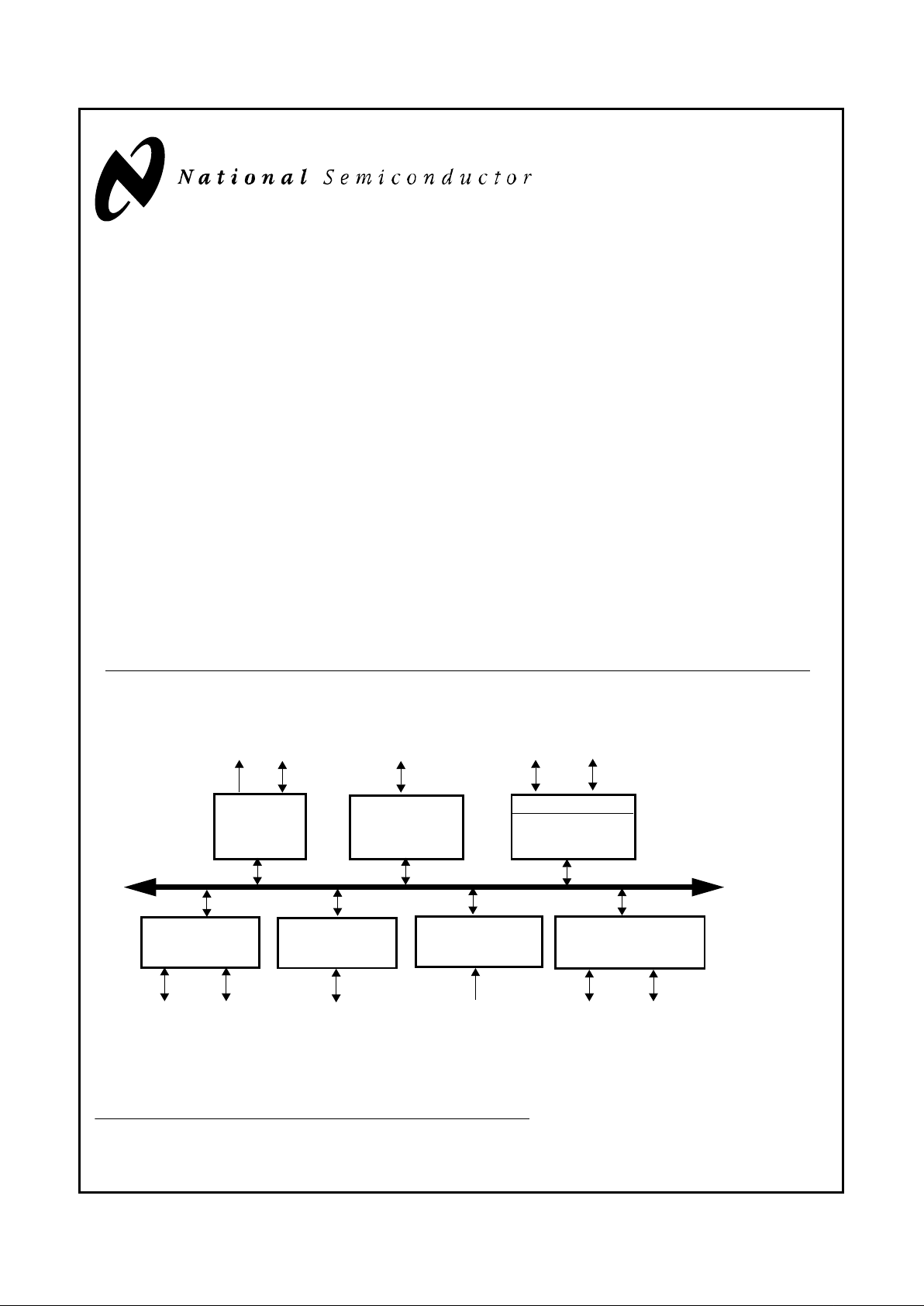
PC87309 Block Diagram
High Current Driver
Controller (KBC)
Power Management
(PM) Logic
µP Address
IEEE 1284
Control
Parallel Port
Ports
(Logical Device 4)
(Logical Devices 5 & 6)
Data and
Control
(Logical Device 0)
(Logical Device 1)
Control
Data and
(PnP)
IRQ
DMA
Channels
Plug and Play
Floppy Disk
Controller (FDC)
Floppy Drive
Interface
Mouse and Keyboard
Data Handshake
Serial
with IR (UART2)
Infrared
(Logical Devices 2)
Serial
(UART1)
Interface
(Logical Devices 3)
Serial Port
Serial Port
TRI-STATE® is a registered trademark of National Semiconductor Corporation.
IBM
®
, MicroChannel®, PC-AT® and PS/2® are registered trademarks of International Business Machines Corporation.
Microsoft
®
and Windows® are registered trademarks of Microsoft Corporation.
Page 2

2
Highlights
www.national.com
Features
●
100% compatibility with PnP requirements specified in
the “
Plug and Play ISA Specification
”, PC97, ISA, EISA,
and MicroChannel architectures
●
A special PnP module that includes:
— Flexible IRQs, DMAs and base addresses that meet
the PnP requirements specified by Microsoft
®
in
their 1995 hardware design guide for Windows
®
and
PnP ISA Revision 1.0A
— PnP ISA mode (with isolation mechanism – Wait for
Key state Motherboard PnP mode
●
A Floppy Disk Controller (FDC) that provides:
— A relocatable address that is referenced by an 11-bit
programmable register
— Software compatibility with the PC8477, which con-
tains a superset of the floppy disk controller functions in the µDP8473, the NEC µPD765A and the
N82077
— 7 IRQ channel options
— Three 8-bit DMA channel options
— 16-byte FIFO
— Burst and non-burst modes
— A new high-performance, on-chip, digital data sepa-
rator that does not require any external filter components
— Support for standard 5.25" and 3.5" floppy disk
drives
— Perpendicular recording drive support
— Three-mode Floppy Disk Drive (FDD) support
— Full suppor t for the IBM Tape Drive Register (TDR)
implementation of AT and PS/2 drive types
●
A Keyboard and mouse Controller (KBC) with:
— A relocatable address that is referenced by an 11-bit
programmable register, reported as a fixed address
in resource data
— 7 IRQ options for the keyboard controller
— 7 IRQ options for the mouse controller
— An 8-bit microcontroller
— Software compatibility with the 8042AH and
PC87911 microcontrollers
— 2 KB of custom-designed program ROM
— 256 bytes of RAM for data
— Three programmable dedicated open drain I/O lines
for keyboard controller applications
— Asynchronous access to two data registers and one
status register during normal operation
— Support for both interrupt and polling
— 93 instructions
— An 8-bit timer/counter
— Support for binary and BCD arithmetic
— Operation at 8 MHz,12 MHz or 16 MHz (programma-
ble option)
— Customizing by using the PC87323VUL, which in-
cludes a RAM-based KBC, as a development platform for keyboard controller code for the PC87309
●
Two UARTs that provide:
— Software compatibility with the 16550A and the 16450
— A relocatable address that is referenced by an 11-bit
programmable register
— 7 IRQ channel options
— Shadow register support for write-only bit monitoring
— UART data rates up to 1.5 Mbaud
●
An enhanced UART and Infrared (IR) interface on the
UART2 that supports:
— HP-SIR
— ASK-IR option of SHARP-IR
— DASK-IR option of SHARP-IR
— Consumer Remote Control circuitry
— A PnP compatible external transceiver
— Three 8-bit DMA options for the UART with Slow In-
frared support (UART2)
●
A bidirectional parallel port that includes:
— A relocatable address that is referenced by an 11-bit
programmable register
— Software or hardware control
— 7 IRQ channel options
— Three 8-bit DMA channel options
— Demand mode DMA support
— An Enhanced Parallel Port (EPP) that is compatible
with the new version EPP 1.9, and is IEEE 1284
compliant
— An Enhanced Parallel Port (EPP) that also supports
version EPP 1.7 of the Xircom specification.
— Support for an Enhanced Parallel Port (EPP) as
mode 4 of the Extended Capabilities Port (ECP)
— An Extended Capabilities Port (ECP) that is IEEE
1284 compliant, including level 2
— Selection of internal pull-up or pull-down resistor for
Paper End (PE) pin
— Reduction of PCI bus utilization by supporting a de-
mand DMA mode mechanism and a DMA fairness
mechanism
— A protection circuit that prevents damage to the par-
allel port when a printer connected to it powers up or
is operated at high voltages
— Output buffers that can sink and source 14 mA
●
Enhanced Power Management (PM), including:
— Reduced current leakage from pins
— Low-power CMOS technology
— Ability to shut off clocks to all modules
●
Clock source:
— Source is a 48 MHz clock input signal.
●
General features include:
— Access to all configuration registers is through an In-
dex and a Data register, which can be relocated
within the ISA I/O address space
— 100-pin Plastic Quad Flatpack (PQFP) package
Page 3
3
Highlights
www.national.com
DRATE0
Parallel
Port
Connector
Configuration
Select Logic
48 MHz
EIA
Drivers
EIA
Drivers
ISA Bus
Basic Configuration
CLKIN
MR
AEN
A11-0
D7-0
RD
WR
TC
PD7-0
SLIN/ASTRB
STB/WRITE
AFD/DSTRB
INIT
ACK
ERR
SLCT
PE
BUSY/
WAIT
BADDR1,0
CFG0
SIN1
SOUT1
RTS1
DTR1/BOUT1
CTS1
DSR1
DCD1
RI1
SIN2
SOUT2
RTS2
DTR2/BOUT2
CTS2
DSR2
DCD2
RI2
RDATA
WDATA
WGATE
HDSEL
DIR
STEP
TRK0
INDEX
DSKCHG
WP
MTR1,0
DR1,0
DENSEL
IOCHRDY
DRQ3-1
DACK3-1
P12
P21,20
KBCLK
KBDAT
MDAT
MCLK
Keyboard I/O
Interface
IRQ1
Infrared (IR)
Interface
IRRX2,1
IRTX
PC87309
IRQ7-3
IRQ12
IRSL2-0
ID3-0
Clock
Floppy
Disk
(FDC)
Controller
Connector
Page 4

4
Table of Contents
www.national.com
Table of Contents
Highlights.......................................................................................................................................................1
1.0 Signal/Pin Connection and Description
1.1 CONNECTION DIAGRAM .........................................................................................................12
1.2 SIGNAL/PIN DESCRIPTIONS ...................................................................................................13
2.0 Configuration
2.1 HARDWARE CONFIGURATION ...............................................................................................19
2.1.1 Wake Up Options ........................................................................................................19
2.1.2 The Index and Data Register Pair ...............................................................................19
2.2 SOFTWARE CONFIGURATION ...............................................................................................20
2.2.1 Accessing the Configuration Registers ........................................................................20
2.2.2 Address Decoding .......................................................................................................20
2.3 THE CONFIGURATION REGISTERS .......................................................................................21
2.3.1 Standard Plug and Play (PnP) Register Definitions ....................................................21
2.3.2 Configuration Register Summary ................................................................................25
2.4 CARD CONTROL REGISTERS ................................................................................................28
2.4.1 SID Register ................................................................................................................28
2.4.2 SuperI/O Configuration 1 Register (SIOCF1) ..............................................................28
2.4.3 SuperI/O Configuration 2 Register (SIOCF2) ..............................................................29
2.4.4 SRID Register ..............................................................................................................29
2.5 FDC CONFIGURATION REGISTERS (LOGICAL DEVICE 0) ..................................................30
2.5.1 SuperI/O FDC Configuration Register .........................................................................30
2.5.2 Drive ID Register .........................................................................................................30
2.6 SUPERI/O PARALLEL PORT CONFIGURATION REGISTER (LOGICAL DEVICE 1) .............30
2.7 SUPERI/O UART2 AND INFRARED CONFIGURATION REGISTER (LOGICAL DEVICE 2) ..31
2.8 SUPERI/O UART1 CONFIGURATION REGISTER (LOGICAL DEVICE 3) ..............................32
2.9 SUPERI/O KBC CONFIGURATION REGISTER (LOGICAL DEVICE 6) ..................................32
2.10 CONFIGURATION REGISTER BITMAPS ................................................................................32
3.0 The Floppy Disk Controller (FDC) (Logical Device 0)
3.1 FDC FUNCTIONS .....................................................................................................................34
3.1.1 Microprocessor Interface .............................................................................................34
3.1.2 System Operation Modes ............................................................................................34
3.2 DATA TRANSFER .....................................................................................................................35
3.2.1 Data Rates ...................................................................................................................35
3.2.2 The Data Separator .....................................................................................................35
3.2.3 Perpendicular Recording Mode Support .....................................................................36
3.2.4 Data Rate Selection .....................................................................................................36
3.2.5 Write Precompensation ...............................................................................................37
3.2.6 FDC Low-Power Mode Logic .......................................................................................37
3.2.7 Reset ...........................................................................................................................37
3.3 THE REGISTERS OF THE FDC ...............................................................................................37
Page 5

5
Table of Contents
www.national.com
3.3.1 Status Register A (SRA) ..............................................................................................38
3.3.2 Status Register B (SRB) ..............................................................................................39
3.3.3 Digital Output Register (DOR) .....................................................................................39
3.3.4 Tape Drive Register (TDR) ..........................................................................................41
3.3.5 Main Status Register (MSR) ........................................................................................42
3.3.6 Data Rate Select Register (DSR) ................................................................................43
3.3.7 Data Register (FIFO) ...................................................................................................43
3.3.8 Digital Input Register (DIR) ..........................................................................................44
3.3.9 Configuration Control Register (CCR) .........................................................................45
3.4 THE PHASES OF FDC COMMANDS .......................................................................................45
3.4.1 Command Phase .........................................................................................................45
3.4.2 Execution Phase ..........................................................................................................45
3.4.3 Result Phase ...............................................................................................................47
3.4.4 Idle Phase ....................................................................................................................47
3.4.5 Drive Polling Phase .....................................................................................................48
3.5 THE RESULT PHASE STATUS REGISTERS ..........................................................................48
3.5.1 Result Phase Status Register 0 (ST0) .........................................................................48
3.5.2 Result Phase Status Register 1 (ST1) .........................................................................49
3.5.3 Result Phase Status Register 2 (ST2) .........................................................................49
3.5.4 Result Phase Status Register 3 (ST3) .........................................................................50
3.6 FDC REGISTER BITMAPS .......................................................................................................51
3.6.1 Standard ......................................................................................................................51
3.6.2 Result Phase Status ....................................................................................................52
3.7 COMMAND SET .......................................................................................................................53
3.7.1 Abbreviations Used in FDC Commands ......................................................................54
3.7.2 The CONFIGURE Command ......................................................................................55
3.7.3 The DUMPREG Command .........................................................................................55
3.7.4 The FORMAT TRACK Command ...............................................................................56
3.7.5 The INVALID Command ..............................................................................................58
3.7.6 The LOCK Command ..................................................................................................60
3.7.7 The MODE Command .................................................................................................60
3.7.8 The NSC Command ....................................................................................................62
3.7.9 The PERPENDICULAR MODE Command .................................................................62
3.7.10 The READ DATA Command .......................................................................................64
3.7.11 The READ DELETED DATA Command ......................................................................66
3.7.12 The READ ID Command .............................................................................................67
3.7.13 The READ A TRACK Command .................................................................................68
3.7.14 The RECALIBRATE Command ...................................................................................68
3.7.15 The RELATIVE SEEK Command ................................................................................69
3.7.16 The SCAN EQUAL, the SCAN LOW OR EQUAL and the SCAN HIGH OR EQUAL
Commands ..................................................................................................................69
3.7.17 The SEEK Command ..................................................................................................70
3.7.18 The SENSE DRIVE STATUS Command ....................................................................71
3.7.19 The SENSE INTERRUPT Command ..........................................................................71
3.7.20 The SET TRACK Command ........................................................................................72
3.7.21 The SPECIFY Command ............................................................................................73
3.7.22 The VERIFY Command ...............................................................................................74
Page 6

6
Table of Contents
www.national.com
3.7.23 The VERSION Command ............................................................................................76
3.7.24 The WRITE DATA Command ......................................................................................76
3.7.25 The WRITE DELETED DATA Command ....................................................................77
3.8 EXAMPLE OF A FOUR-DRIVE CIRCUIT USING THE PC87309 .............................................78
4.0 Parallel Port (Logical Device 1)
4.1 PARALLEL PORT CONFIGURATION ......................................................................................79
4.1.1 Parallel Port Operation Modes ....................................................................................79
4.1.2 Configuring Operation Modes ......................................................................................79
4.1.3 Output Pin Protection ..................................................................................................79
4.2 STANDARD PARALLEL PORT (SPP) MODES ........................................................................79
4.2.1 SPP Modes Register Set .............................................................................................80
4.2.2 SPP Data Register (DTR) ............................................................................................80
4.2.3 Status Register (STR) .................................................................................................81
4.2.4 SPP Control Register (CTR) ........................................................................................81
4.3 ENHANCED PARALLEL PORT (EPP) MODES ........................................................................82
4.3.1 EPP Register Set .........................................................................................................82
4.3.2 SPP or EPP Data Register (DTR) ...............................................................................83
4.3.3 SPP or EPP Status Register (STR) .............................................................................83
4.3.4 SPP or EPP Control Register (CTR) ...........................................................................83
4.3.5 EPP Address Register (ADDR) ...................................................................................83
4.3.6 EPP Data Register 0 (DATA0) ....................................................................................84
4.3.7 EPP Data Register 1 (DATA1) ....................................................................................84
4.3.8 EPP Data Register 2 (DATA2) ....................................................................................84
4.3.9 EPP Data Register 3 (DATA3) ....................................................................................84
4.3.10 EPP Mode Transfer Operations ..................................................................................85
4.3.11 EPP 1.7 and 1.9 Data Write and Read Operations .....................................................85
4.4 EXTENDED CAPABILITIES PARALLEL PORT (ECP) .............................................................86
4.4.1 ECP Modes .................................................................................................................86
4.4.2 Software Operation ......................................................................................................86
4.4.3 Hardware Operation ....................................................................................................87
4.5 ECP MODE REGISTERS ..........................................................................................................87
4.5.1 Accessing the ECP Registers ......................................................................................87
4.5.2 Second Level Offsets ..................................................................................................88
4.5.3 ECP Data Register (DATAR) .......................................................................................88
4.5.4 ECP Address FIFO (AFIFO) Register .........................................................................88
4.5.5 ECP Status Register (DSR) .........................................................................................88
4.5.6 ECP Control Register (DCR) .......................................................................................89
4.5.7 Parallel Port Data FIFO (CFIFO) Register ...................................................................90
4.5.8 ECP Data FIFO (DFIFO) Register ...............................................................................90
4.5.9 Test FIFO (TFIFO) Register ........................................................................................90
4.5.10 Configuration Register A (CNFGA) .............................................................................90
4.5.11 Configuration Register B (CNFGB) .............................................................................91
4.5.12 Extended Control Register (ECR) ...............................................................................91
4.5.13 ECP Extended Index Register (EIR) ...........................................................................92
4.5.14 ECP Extended Data Register (EDR) ...........................................................................93
Page 7

7
Table of Contents
www.national.com
4.5.15 ECP Extended Auxiliary Status Register (EAR) ..........................................................93
4.5.16 Control0 Register .........................................................................................................93
4.5.17 Control2 Register .........................................................................................................93
4.5.18 Control4 Register .........................................................................................................94
4.5.19 PP Confg0 Register .....................................................................................................94
4.6 DETAILED ECP MODE DESCRIPTIONS .................................................................................95
4.6.1 Software Controlled Data Transfer (Modes 000 and 001) ...........................................95
4.6.2 Automatic Data Transfer (Modes 010 and 011) ..........................................................95
4.6.3 Automatic Address and Data Transfers (Mode 100) ...................................................97
4.6.4 FIFO Test Access (Mode 110) ....................................................................................97
4.6.5 Configuration Registers Access (Mode 111) ...............................................................97
4.6.6 Interrupt Generation ....................................................................................................97
4.7 PARALLEL PORT REGISTER BITMAPS .................................................................................98
4.7.1 EPP Modes ..................................................................................................................98
4.7.2 ECP Modes .................................................................................................................99
4.8 PARALLEL PORT PIN/SIGNAL LIST ......................................................................................101
5.0 Enhanced Serial Port with IR -UART2 (Logical Device 2)
5.1 FEATURES ..............................................................................................................................102
5.2 FUNCTIONAL MODES OVERVIEW .......................................................................................102
5.2.1 UART Modes: 16450 or 16550, and Extended ..........................................................102
5.2.2 Sharp-IR, IrDA SIR Infrared Modes ...........................................................................102
5.2.3 Consumer IR Mode ...................................................................................................102
5.3 REGISTER BANK OVERVIEW ...............................................................................................102
5.4 UART MODES – DETAILED DESCRIPTION ..........................................................................104
5.4.1 16450 or 16550 UART Mode .....................................................................................104
5.4.2 Extended UART Mode ...............................................................................................104
5.5 SHARP-IR MODE – DETAILED DESCRIPTION .....................................................................105
5.6 SIR MODE – DETAILED DESCRIPTION ................................................................................105
5.7 CONSUMER-IR MODE – DETAILED DESCRIPTION ............................................................105
5.7.1 Consumer-IR Transmission .......................................................................................105
5.7.2 Consumer-IR Reception ............................................................................................106
5.8 FIFO TIME-OUTS ....................................................................................................................106
5.8.1 UART, SIR or Sharp-IR Mode Time-Out Conditions .................................................106
5.8.2 Consumer-IR Mode Time-Out Conditions .................................................................106
5.8.3 Transmission Deferral ...............................................................................................107
5.9 AUTOMATIC FALLBACK TO A NON-EXTENDED UART MODE ..........................................107
5.11 BANK 0 – GLOBAL CONTROL AND STATUS REGISTERS .................................................107
5.11.1 Receiver Data Port (RXD) or the Transmitter Data Port (TXD) .................................108
5.11.2 Interrupt Enable Register (IER) .................................................................................108
5.11.3 Event Identification Register (EIR) ............................................................................110
5.11.4 FIFO Control Register (FCR) .....................................................................................112
5.11.5 Link Control Register (LCR) and Bank Selection Register (BSR) .............................112
5.11.6 Bank Selection Register (BSR) .................................................................................113
5.11.7 Modem/Mode Control Register (MCR) ......................................................................114
Page 8

8
Table of Contents
www.national.com
5.11.8 Link Status Register (LSR) ........................................................................................115
5.11.9 Modem Status Register (MSR) ..................................................................................116
5.11.10 Scratchpad Register (SPR) .......................................................................................117
5.11.11 Auxiliary Status and Control Register (ASCR) ..........................................................117
5.12 BANK 1 – THE LEGACY BAUD GENERATOR DIVISOR PORTS .........................................117
5.12.1 Legacy Baud Generator Divisor Ports (LBGD(L) and LBGD(H)), ..............................118
5.12.2 Link Control Register (LCR) and Bank Select Register (BSR) ..................................118
5.13 BANK 2 – EXTENDED CONTROL AND STATUS REGISTERS ............................................118
5.13.1 Baud Generator Divisor Ports, LSB (BGD(L)) and MSB (BGD(H)) ...........................119
5.13.2 Extended Control Register 1 (EXCR1) ......................................................................120
5.13.3 Link Control Register (LCR) and Bank Select Register (BSR) ..................................121
5.13.4 Extended Control and Status Register 2 (EXCR2) ....................................................121
5.13.5 Reserved Register .....................................................................................................121
5.13.6 TX_FIFO Current Level Register (TXFLV) ................................................................121
5.13.7 RX_FIFO Current Level Register (RXFLV) ...............................................................122
5.14 BANK 3 – MODULE REVISION ID AND SHADOW REGISTERS ..........................................122
5.14.1 Module Revision ID Register (MRID) ........................................................................122
5.14.2 Shadow of Link Control Register (SH_LCR) .............................................................122
5.14.3 Shadow of FIFO Control Register (SH_FCR) ............................................................123
5.14.4 Link Control Register (LCR) and Bank Select Register (BSR) ..................................123
5.15 BANK 4 – IR MODE SETUP REGISTER ................................................................................123
5.15.1 Reserved Registers ...................................................................................................123
5.15.2 Infrared Control Register 1 (IRCR1) ..........................................................................123
5.15.3 Link Control Register (LCR) and Bank Select Register (BSR) ..................................123
5.15.4 Reserved Registers ...................................................................................................123
5.16 BANK 5 – INFRARED CONTROL REGISTERS .....................................................................123
5.16.1 Reserved Registers ...................................................................................................124
5.16.2 (LCR/BSR) Register ..................................................................................................124
5.16.3 Infrared Control Register 2 (IRCR2) ..........................................................................124
5.16.4 Reserved Registers ...................................................................................................124
5.17 BANK 6 – INFRARED PHYSICAL LAYER CONFIGURATION REGISTERS .........................124
5.17.1 Infrared Control Register 3 (IRCR3) ..........................................................................124
5.17.2 Reserved Register .....................................................................................................124
5.17.3 SIR Pulse Width Register (SIR_PW) .........................................................................124
5.17.4 Link Control Register (LCR) and Bank Select Register (BSR) ..................................125
5.17.5 Reserved Registers ...................................................................................................125
5.18 BANK 7 – CONSUMER-IR AND OPTICAL TRANSCEIVER CONFIGURATION REGISTERS 125
5.18.1 Infrared Receiver Demodulator Control Register (IRRXDC) .....................................125
5.18.2 Infrared Transmitter Modulator Control Register (IRTXMC) ......................................126
5.18.3 Consumer-IR Configuration Register (RCCFG) ........................................................128
5.18.4 Link Control/Bank Select Registers (LCR/BSR) ........................................................129
5.18.5 Infrared Interface Configuration Register 1 (IRCFG1) ...............................................129
5.18.6 Reserved Register .....................................................................................................129
5.18.7 Infrared Interface Configuration 3 Register (IRCFG3) ...............................................129
5.18.8 Infrared Interface Configuration Register 4 (IRCFG4) ...............................................130
5.19 UART2 WITH IR REGISTER BITMAPS ..................................................................................131
Page 9

9
Table of Contents
www.national.com
6.0 Enhanced Serial Port - UART1 (Logical Device 3)
6.1 REGISTER BANK OVERVIEW ...............................................................................................136
6.2 DETAILED DESCRIPTION ......................................................................................................136
6.2.1 16450 or 16550 UART Mode .....................................................................................137
6.2.2 Extended UART Mode ...............................................................................................137
6.3 FIFO TIME-OUTS ....................................................................................................................137
6.4 AUTOMATIC FALLBACK TO A NON-EXTENDED UART MODE ..........................................138
6.4.1 Transmission Deferral ...............................................................................................138
6.5 BANK 0 – GLOBAL CONTROL AND STATUS REGISTERS .................................................138
6.5.1 Receiver Data Port (RXD) or the Transmitter Data Port (TXD) .................................138
6.5.2 Interrupt Enable Register (IER) .................................................................................139
6.5.3 Event Identification Register (EIR) ............................................................................140
6.5.4 FIFO Control Register (FCR) .....................................................................................142
6.5.5 Line Control Register (LCR) and Bank Selection Register (BSR) .............................142
6.5.6 Bank Selection Register (BSR) .................................................................................143
6.5.7 Modem/Mode Control Register (MCR) ......................................................................143
6.5.8 Line Status Register (LSR) ........................................................................................144
6.5.9 Modem Status Register (MSR) ..................................................................................145
6.5.10 Scratchpad Register (SPR) .......................................................................................146
6.5.11 Auxiliary Status and Control Register (ASCR) ..........................................................146
6.6 BANK 1 – THE LEGACY BAUD GENERATOR DIVISOR PORTS .........................................146
6.6.1 Legacy Baud Generator Divisor Ports (LBGD(L) and LBGD(H)), ..............................147
6.6.2 Line Control Register (LCR) and Bank Select Register (BSR) ..................................147
6.7 BANK 2 – EXTENDED CONTROL AND STATUS REGISTERS ............................................148
6.7.1 Baud Generator Divisor Ports, LSB (BGD(L)) and MSB (BGD(H)) ...........................148
6.7.2 Extended Control Register 1 (EXCR1) ......................................................................149
6.7.3 Line Control Register (LCR) and Bank Select Register (BSR) ..................................149
6.7.4 Extended Control and Status Register 2 (EXCR2) ....................................................149
6.7.5 Reserved Register .....................................................................................................150
6.7.6 TX_FIFO Current Level Register (TXFLV) ................................................................150
6.7.7 RX_FIFO Current Level Register (RXFLV) ...............................................................150
6.8 BANK 3 – MODULE REVISION ID AND SHADOW REGISTERS ..........................................150
6.8.1 Module Revision ID Register (MRID) ........................................................................151
6.8.2 Shadow of Line Control Register (SH_LCR) .............................................................151
6.8.3 Shadow of FIFO Control Register (SH_FCR) ............................................................151
6.8.4 Line Control Register (LCR) and Bank Select Register (BSR) ..................................151
6.9 UART1 REGISTER BITMAPS .................................................................................................151
7.0 Power Management (Logical Device 4)
7.1 POWER MANAGEMENT OPTIONS .......................................................................................155
7.2 THE POWER MANAGEMENT REGISTERS ..........................................................................155
7.2.1 Power Management Index Register ..........................................................................155
7.2.2 Power Management Data Register ...........................................................................155
7.2.3 Function Enable Register 1 (FER1) ...........................................................................155
7.2.4 Power Management Control Register (PMC1) ..........................................................156
Page 10

10
Table of Contents
www.national.com
7.2.5 Power Management Control 3 Register (PMC3) .......................................................156
7.3 POWER MANAGEMENT REGISTER BITMAPS ....................................................................157
8.0 Mouse and Keyboard Controller (KBC) (Logical Devices 5 and 6)
8.1 SYSTEM ARCHITECTURE .....................................................................................................158
8.2 FUNCTIONAL OVERVIEW .....................................................................................................159
8.3 DEVICE CONFIGURATION ....................................................................................................159
8.3.1 I/O Address Space ....................................................................................................159
8.3.2 Interrupt Request Signals ..........................................................................................159
8.3.3 KBC Clock .................................................................................................................161
8.3.4 Timer or Event Counter .............................................................................................161
8.4 EXTERNAL I/O INTERFACES ................................................................................................161
8.4.1 Keyboard and Mouse Interface .................................................................................161
8.4.2 General Purpose I/O Signals .....................................................................................162
8.5 INTERNAL KBC - PC87309 INTERFACE ...............................................................................163
8.5.1 The KBC DBBOUT Register, Offset 60h, Read Only ................................................163
8.5.2 The KBC DBBIN Register, Offset 60h (F1 Clear) or 64h (F1 Set), Write Only ..........163
8.5.3 The KBC STATUS Register ......................................................................................163
8.6 INSTRUCTION TIMING ...........................................................................................................163
9.0 Interrupt and DMA Mapping
9.1 IRQ MAPPING .........................................................................................................................164
9.2 DMA MAPPING .......................................................................................................................164
10.0 Device Specifications
10.1 GENERAL DC ELECTRICAL CHARACTERISTICS ...............................................................165
10.1.1 Recommended Operating Conditions .......................................................................165
10.1.2 Absolute Maximum Ratings .......................................................................................165
10.1.3 Capacitance ...............................................................................................................165
10.1.4 Power Consumption under Recommended Operating Conditions ............................165
10.2 DC CHARACTERISTICS OF PINS, BY GROUP ....................................................................166
10.2.1 Group 1 ......................................................................................................................166
10.2.2 Group 2 ......................................................................................................................166
10.2.3 Group 3 ......................................................................................................................166
10.2.4 Group 4 ......................................................................................................................167
10.2.5 Group 5 ......................................................................................................................167
10.2.6 Group 6 ......................................................................................................................167
10.2.7 Group 7 ......................................................................................................................168
10.2.8 Group 8 ......................................................................................................................168
10.2.9 Group 9 ......................................................................................................................169
10.2.10 Group 10 ....................................................................................................................169
10.2.11 Group 11 ....................................................................................................................169
10.2.12 Group 12 ....................................................................................................................169
10.2.13 Group 13 ....................................................................................................................170
10.2.14 Group 14 ....................................................................................................................170
Page 11

11
Table of Contents
www.national.com
10.2.15 Group 15 ....................................................................................................................170
10.2.16 Group 18 ....................................................................................................................170
10.3 AC ELECTRICAL CHARACTERISTICS ..................................................................................171
10.3.1 AC Test Conditions ....................................................................................................171
10.3.2 Clock Timing ..............................................................................................................171
10.3.3 Microprocessor Interface Timing ...............................................................................172
10.3.4 Baud Output Timing ...................................................................................................174
10.3.5 Transmitter Timing .....................................................................................................175
10.3.6 Receiver Timing .........................................................................................................176
10.3.7 UART, Sharp-IR, SIR and Consumer Remote Control Timing ..................................178
10.3.8 IRSLn Write Timing ...................................................................................................179
10.3.9 Modem Control Timing ..............................................................................................179
10.3.10 FDC DMA Timing ......................................................................................................180
10.3.11 ECP DMA Timing ......................................................................................................181
10.3.12 UART2 DMA Timing ..................................................................................................182
10.3.13 Reset Timing .............................................................................................................183
10.3.14 FDC - Write Data Timing ...........................................................................................183
10.3.15 FDC - Drive Control Timing .......................................................................................184
10.3.16 FDC - Read Data Timing ...........................................................................................184
10.3.17 Standard Parallel Port Timing ....................................................................................185
10.3.18 Enhanced Parallel Port 1.7 Timing ............................................................................186
10.3.19 Enhanced Parallel Port 1.9 Timing ............................................................................187
10.3.20 Extended Capabilities Port (ECP) Timing ..................................................................188
Glossary .....................................................................................................................................................189
Page 12
Signal/Pin Connection and Description
12
1.0 Signal/Pin Connection and Description
www.national.com
1.0 Signal/Pin Connection and Description
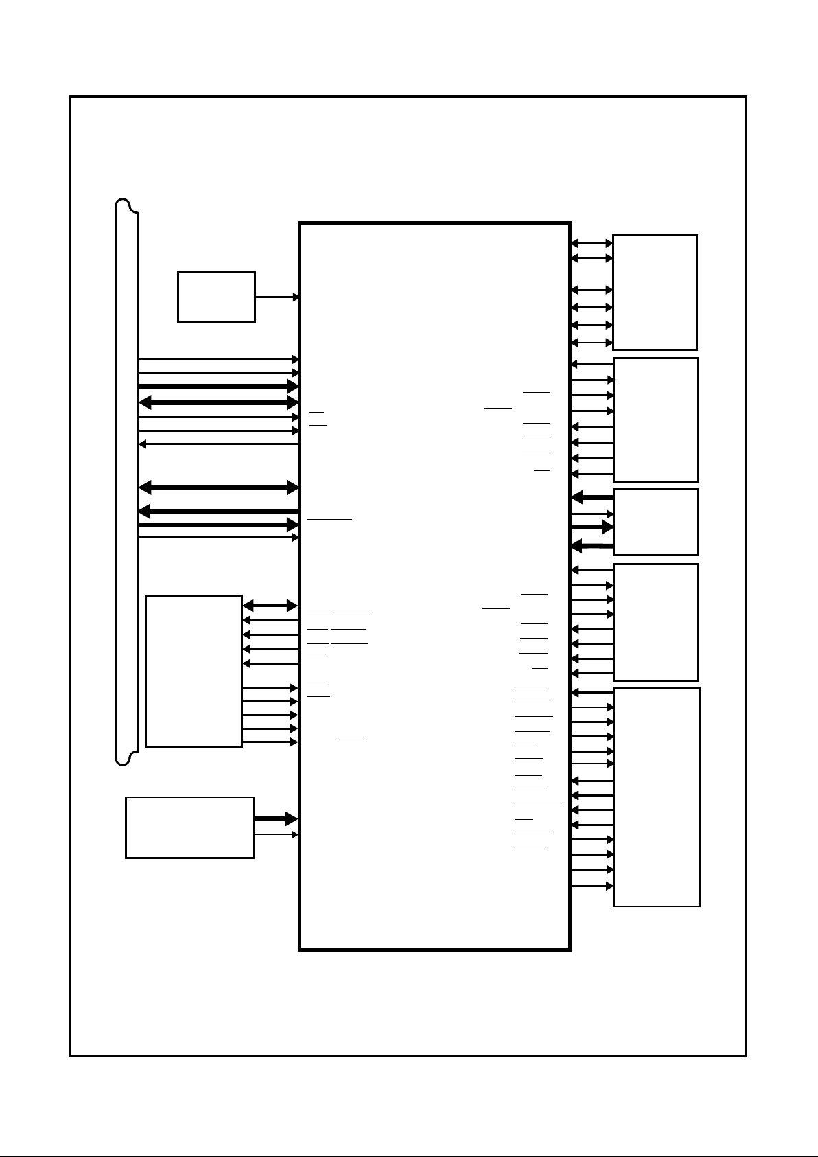
1.1 CONNECTION DIAGRAM
80 79 78 77 76 75 74 73 72 71 70 69 68 67 66 65 64 63 62 61 60 59 58 57 56 55 54 53 52 51
1 2 3 4 5 6 7 8 9 101112131415161718192021222324252627282930
81
82
83
84
85
86
87
88
89
90
91
92
93
94
95
96
97
98
99
100
50
49
48
47
46
45
44
43
42
41
40
39
38
37
36
35
34
33
32
31
DIR
WDATA
DR1/DENSEL
DR0
MTR1/P12
MTR0/DRATE0
IRTX/DENSEL
IRRX1/P12/DRATE0
DACK3
VDD
VSS
DACK2
DACK1
DRQ3
DRQ2
DRQ1
MR
IRQ12
IRQ7
PD6
PD7
CTS1
DCD1
DSR1
BOUT1/
DTR1/BADDR0
RI1
RTS1/BADDR1
SIN1
VDD
VSS
SOUT1/CGF0
CTS2/A11
DCD2/P12
DSR2/DRATE0
BOUT2/
DTR2/IRSL2/ID2
RI2/DENSEL
RTS2/IRSL1/ID1
SIN2/ID3
SOUT2/IRSL0/IRRX2/ID0
PD5
PD4
PD3
PD2
PD0
AFD/DSTRB
SLIN/ASTRB
INIT
ERRPESLCT
ACK
STB/WRITE
BUSY/WAIT
VSS
P21
P20
MDAT
MCLK
KBCLK
INDEX
TRK0
WGATE
HDSEL
STEP
PD1
D0D1D2
D5D6D7
A0A1A2A3A4
A5
VSS
A6A7A8
A9
A10
AEN
IOCHRDY
IORD
IOWR
TC
IRQ1
IRQ3
IRQ4
IRQ5
IRQ6
PC87309VLJ
RDATA
D4
D3
CLKIN
KBDAT
DSKCHG
WP
Page 13

Signal/Pin Connection and Description
SIGNAL/PIN DESCRIPTIONS
13
www.national.com
1.2 SIGNAL/PIN DESCRIPTIONS
TABLE 1-1 lists the signals of the PC87309 in alphabetical
order and shows the pin(s) associated with each. TABLE
1-2 on page 18 lists the signals that are multiplexed in FullIR and Two-UART modes. TABLE 1-3 on page 18 lists the
pins that have strap functions during reset.
The Module column indicates the functional module that is
associated with these pins. In this column, the System label
indicates internal functions that are common to more than
one module. The I/O and Group # column describes whether the pin is an input, output, or bidirectional pin (marked as
Input, Output or I/O, respectively).
TABLE 1-1. Signal/Pin Description Table
Signal/Pin
Name
Pin
Number
Module
I/O and
Group #
Function
A11-0 93, 20-16,
14-9
ISA-Bus Input
Group 1
ISA-Bus Address – A11-0 are used for address decoding on any
access except DMA accesses, on the condition that the AEN signal is
low.
A11 is multiplexed with
CTS2 on pin 93 and available in Full-IR mode
only. Since A11 is required to suppor t full ISA PnP mode (for
decoding A79h), this mode is not available in Two-UART mode.
See Section 2.2.2.
ACK 68 Parallel Por t Input
Group 3
Acknowledge – This input signal is pulsed low by the printer to
indicate that it has received data from the parallel port. This pin is
internally connected to an internal weak pull-up.
AFD 74 Parallel Port I/O
Group 8
Automatic Feed – When this signal is low the printer should
automatically feed a line after printing each line. This pin is in TRISTATE after a 0 is loaded into the corresponding control register bit.
An external 4.7 KΩ pull-up resistor should be attached to this pin.
This signal is multiplexed with
DSTRB. See TABLE 4-12 on page 101
for more information.
AEN 21 ISA-Bus Input
Group 1
DMA Address Enable – This input signal disables function selection
via A11-0 when it is high. Access during DMA transfer is not affected
by this signal. This pin is used for external decoding of A11-15 in
Two-UART mode or A15-12 in Full-IR mode.
ASTRB 73 Parallel Port Output
Group 8
Address Strobe (EPP) – This signal is used in EPP mode as an
address strobe. It is active low.
This signal is multiplexed with
SLIN. See TABLE 4-12 on page 101 for
more information.
BADDR1,0 88,86 Configuration Input
Group 4
Base Address Strap Pins 0 and 1 – These pins determine the base
addresses of the Index and Data registers, the value of the Plug and
Play ISA Serial Identifier and the configuration state immediately after
reset. These pins are pulled down by internal 30 KΩ resistors.
External 10 KΩ pull-up resistors to V
DD
should be employed.
BADDR1 is multiplexed with
RTS1.
BADDR0 is multiplexed with
DTR1 and BOUT1.
See TABLE 2-1 and Section 2.1.
BOUT2,1 96,86 UART1,
UART 2
Output
Group 12
Baud Output – This multi-function pin provides the associated serial
channel Baud Rate generator output signal if test mode is selected,
i.e., bit 7 of the EXCR1 register is set. See “Bit 7 - Baud Generator
Test (BTEST)” on page 121.
After Master Reset this pin provides the DTR function.
BOUT2 is multiplexed with DTR2, IRSL2 and ID2.
BOUT1 is multiplexed with DRT1 and BADDR0.
BUSY 66 Parallel Port Input
Group 2
Busy – This pin is set high by the printer when it cannot accept
another character. It is internally connected to a weak pull-down
resistor.
This signal is multiplexed with
WAIT. See TABLE 4-12 on page 101 for
more information.
Page 14

Signal/Pin Connection and Description
14
SIGNAL/PIN DESCRIPTIONS
www.national.com
CFG0 92 Configuration Input
Group 4
This pin selects between Full-IR and Two-UART mode as the default
configuration upon power up. It is pulled down by internal 30 KΩ
resistors. External 10 KΩ pull-up resistors to V
DD
should be
employed.
This signal is multiplexed with SOUT1.
See TABLE 2-1 and Section 2.1.
CLKIN 33 Clock Input
Group 1
Clock In – A TTL or CMOS compatible 48 MHz clock.
CTS2,1 93,83 UART1,
UART 2
Input
Group 1
UART1 and UART2 Clear to Send – When low, these signals indicate
that the modem or other data transfer device is ready to exchange data.
CTS2 is multiplexed with A11, and available only in Two-UART mode.
D7-0 8-1 ISA-Bus I/O
Group 5
ISA-Bus Data – Bidirectional data lines to the microprocessor. D0 is
the LSB and D7 is the MSB. These signals have 24 mA (sink)
buffered outputs.
DACK3
DACK2,14239,38
ISA-Bus Input
Group 1
DMA Acknowledge 1,2 and 3 – These active low input signals
acknowledge a request for DMA services and enable the
IOWR and
IORD input signals during a DMA transfer. These DMA signals can be
mapped to the following logical devices: FDC, UART or Parallel Por t.
DCD2,1 94,84 UART1,
UART 2
Input
Group 1
UART1 and UART2 Data Carrier Detected – When low, this signal
indicates that the modem or other data transfer device has detected
the data carrier.
DCD2 is multiplexed with P12 and available only in Two-UART mode.
DENSEL 97, 48 or
44
FDC Output
Group 11
Density Select – Indicates that a high FDC density data rate (500
Kbps or 1 Mbps) or a low density data rate (250 or 300 Kbps) is
selected.
DENSEL polarity is controlled by bit 5 of the SuperI/O FDC
Configuration register as described in Section 2.5.1.
This signal is multiplexed with: IRTX, ,
DR1, or R12.
DIR 50 FDC Output
Group 11
Direction – This output signal determines the direction of the Floppy
Disk Drive (FDD) head movement (active = step in, inactive = step
out) during a seek operation. During reads or writes,
DIR is inactive.
DR1,0 48, 47 FDC Output
Group 11
Drive Select 0 and 1 – These active low output signals are the
decoded drive select output signals.
DR0 and DR1 are controlled by
Digital Output Register (DOR) bits 0 and 1. They are encoded with
information to control four FDDs when bit 7 of the SuperI/O FDC
Configuration register is 1, as described in Section 2.5.1.
DR0 can optionally become a logical OR of DR0 and MTR0 when
MTR0/DRATE0 is used as DRATE0.
DR1 is multiplexed with DENSEL and is available only in Two-UART
mode. Optionally, it can become a logical OR of
DR1 and MTR1
when
MTR1/P12 is used as P12.
See
MTR0,1 for more information.
DRATE0 95, 45 or
43
FDC Output
Group 14
Data Rate 0 – This output signal reflects the value of bit 0 of the
Configuration Control Register (CCR) or the Data Rate Select Register
(DSR), whichever was written to last. Output from the pin is totem-pole
buffered (6 mA sink, 6 mA source).
This signal is multiplexed with IRRX1/P12,
MTR0 or DSR2
DRQ3-1 37-35 ISA-Bus Output
Group 13
DMA Request 1, 2 and 3 – These active high output signals inform
the DMA controller that a data transfer is needed. These DMA signals
can be mapped to the following logical devices: Floppy Disk Controller
(FDC), UART or parallel port.
DSKCHG 58 FDC Input
Group 1
Disk Change – This input signal indicates whether or not the drive
door has been opened. The state of this pin is available from the
Digital Input Register (DIR). This pin can also be configured as the
RGATE data separator diagnostic input signal via the MODE
command. See the MODE command in Section 3.7.7.
Signal/Pin
Name
Pin
Number
Module
I/O and
Group #
Function
Page 15

Signal/Pin Connection and Description
SIGNAL/PIN DESCRIPTIONS
15
www.national.com
DSR2,1 95,85 UART1,
UART2
Input
Group 1
Data Set Ready – When low, this signal indicates that the data
transfer device, e.g., modem, is ready to establish a communications
link.
DSR2 is multiplexed with DRATE0 and available only in Two-UART
mode.
DSTRB 74 Parallel Por t Output
Group 8
Data Strobe – This signal is used in EPP mode as a data strobe. It
is active low.
DSTRB is multiplexed with AFD. See TABLE 4-12 on page 101 fo r
more information.
DTR2,1 96,86 UART1,
UART 2
Output
Group 12
Data Terminal Ready – When low, this output signal indicates to the
modem or other data transfer device that the UART1 or UART2 is
ready to establish a communications link.
A Master Reset (MR) deactivates this signal high, and loopback
operation holds this signal inactive.
DTR1 is multiplexed with BADDR0 and with BOUT1.
DTR2 is multiplexed with IRSL2/ID2/BOUT2 and is available only in
Two-UART mode. (BOUT2 is multiplexed implicitly and controlled by
UART2.)
ERR 71 Parallel Port Input
Group 3
Error – This input signal is set active low by the printer when it has
detected an error. This pin is internally connected to an internal weak
pull-up.
HDSEL 52 FDC Output
Group 11
Head Select – This output signal determines which side of the FDD
is accessed. Active low selects side 1, inactive selects side 0.
ID3
ID2
ID1
ID0
99
96
98
100
UART2 Input
Group 1
Identification – These ID signals identify the infrared transceiver for
Plug and Play support. These pins are read after reset.
ID0,1,2 are multiplexed implicitly with IRSL0,1,2 respectively by the
UART2 cell.
ID3 is multiplexed with SIN2.
ID2 is multiplexed with BOUT2,
DTR2, IRSL2.
ID1 is multiplexed with
RTS2, IRSL1
ID0 is multiplexed with SOUT2,IRSL0, IRRX2
INDEX 56 FDC Input
Group 1
Index – This input signal indicates the beginning of an FDD track.
INIT 72 Parallel Port I/O
Group 8
Initialize – When this signal is active low, it causes the printer to be
initialized. This signal is in TRI-STATE after a 1 is loaded into the
corresponding control register bit.
An external 4.7 KΩ pull-up resistor should be employed.
IOCHRDY 22 ISA-Bus Output
Group 15
I/O Channel Ready – This is the I/O channel ready open drain output
signal. When IOCHRDY is dr iven low, the EPP extends the host cycle.
IORD 23 ISA-Bus Input
Group 1
I/O Read – An active low RD input signal indicates that the
microprocessor has read data.
IOWR 24 ISA-Bus Input
Group 1
I/O Write – WR is an active low input signal that indicates a write
operation from the microprocessor to the controller.
IRQ1
IRQ7-3
IRQ12
26
31-27
32
ISA-Bus I/O
Group 10
Interrupt Requests 1, 3, 4, 5, 6, 7 and 12 – IRQ polarity and pushpull or open-drain output selection is software configurable by the
logical device mapped to the IRQ line.
Keyboard Controller (KBC) or Mouse interrupts can be configured by
the Interrupt Request Type Select 0 register (index 71h) as either
edge or level.
IRRX2,1 100,43 UART2 Input
Group 18
Infrared Reception 1 and 2 – Infrared serial input data.
IRRX1 is multiplexed with P12/DRATE0 and is available only in Two-
UART mode.
IRRX2 is multiplexed with SOUT2/IRSL0/ID0 and is available only in
Full-IR mode.
Signal/Pin
Name
Pin
Number
Module
I/O and
Group #
Function
Page 16

Signal/Pin Connection and Description
16
SIGNAL/PIN DESCRIPTIONS
www.national.com
IRSL0
IRSL1
IRSL2
100
98
96
UART2 Output
Group 12
Infrared Control Signals 0, 1 and 2 – These signals control the
Infrared analog front end. The pins on which these signals are driven
is determined by the SuperI/O Configuration 2 register (index 22h).
SeeTABLE 1-2 for more information.
IRSL0 is multiplexed on pin 100 with SOUT2, IRRX2 and ID0, and is
available only in Full-IR mode.
IRSL1 is multiplexed on pin 98 with
RTS2 and ID1, and is available
only in Full-IR mode.
IRSL2 is multiplexed on pin 96 with
DTR2, BOUT2 and ID2, and is
available only in Full-IR mode.
IRTX 44 UART2 Output
Group 12
Infrared Transmit – Infrared serial output data.
This signal is multiplexed with DENSEL only in Two-UART mode.
KBCLK 59 KBC I/O
Group 6
Keyboard Clock – This I/O pin transfers the keyboard clock between
the SuperI/O chip and the external keyboard using the PS/2 protocol.
This pin is connected internally to the internal TO signal of the KBC.
KBDAT 60 KBC I/O
Group 6
Keyboard Data – This I/O pin transfers the keyboard data between
the SuperI/O chip and the external keyboard using the PS/2 protocol.
This pin is connected internally to KBC’s P10.
MCLK 61 KBC I/O
Group 6
Mouse Clock – This I/O pin transfers the mouse clock between the
SuperI/O chip and the external keyboard using the PS/2 protocol.
This pin is connected internally to KBC’s T1.
MDAT 62 KBC I/O
Group 6
Mouse Data – This I/O pin transfers the mouse data between the
SuperI/O chip and the external keyboard using the PS/2 protocol.
This pin is connected internally to KBC’s P11.
MR 34 ISA-Bus Input
Group 1
Master Reset – An active high MR input signal resets the controller
to the idle state, and resets all disk interface output signals to their
inactive states. MR also clears the DOR, DSR and CCR registers,
and resets the MODE command, CONFIGURE command, and LOCK
command parameters to their default values. MR does not affect the
SPECIFY command parameters. MR sets the configuration registers
to their selected default values.
MTR1,0 46,45 FDC Output
Group 11
Motor Select 1,0 – These motor enable lines for drives 0 and 1 are
controlled by bits D7-4 of the Digital Output Register (DOR). They are
output signals that are active when they are low. They are encoded with
information to control four FDDs when bit 7 of the SuperI/O FDC
Configuration register is set See TABLE 1-2 for more information. See
DR1,0.
MTR0 is multiplexed with DRATE0 only in Two-UART mode.
MTR1 is multiplexed with P12 only in Two-UART mode.
P12 94, 46 or
43
KBC I/O
Group 7
I/O Port – KBC quasi-bidirectional port for general purpose input and
output.
P12 is multiplexed on pin 43 with IRRX1 and DRATE0, on pin 46 with
MTR1, and on pin 94 with DCD2.
P21,P20 64,63 KBC I/O
Group 7
I/O Port – KBC open-drain signals for general purpose input and
output. These signals are controlled by KBC firmware.
PD7-0 82-75 Parallel Por t I/O
Group 9
Parallel Port Data – These bidirectional signals transfer data to and
from the peripheral data bus and the appropriate parallel port data
register. These signals have a high current dr ive capability. See
Section 10.1.
PE 70 Parallel Port Input
Group 2
Group 3
Paper End – This input signal is set high by the printer when it is out
of paper. This pin has an internal weak pull-up or pull-down resistor.
RDATA 54 FDC Input
Group 1
Read Data – This input signal holds raw serial data read from the
Floppy Disk Drive (FDD).
Signal/Pin
Name
Pin
Number
Module
I/O and
Group #
Function
Page 17

Signal/Pin Connection and Description
SIGNAL/PIN DESCRIPTIONS
17
www.national.com
RI2,1 97,87 UART1 Input
Group 1
Ring Indicators (Modem) – When low, this signal indicates that a
telephone ring signal has been received by the modem.
The
RI1 and RI2 pins have schmitt-trigger input buffers.
RI2 is multiplexed with DENSEL and available only in Two-UART
mode.
RTS2,1 98,88 UART1,
UART 2
Output
Group 12
Request to Send – When low, these output signals indicate to the
modem or other data transfer device that the corresponding UART1
or UART2 is ready to exchange data.
A Master Reset (MR) sets
RTS to inactive high. Loopback operation
holds it inactive.
RTS2 is multiplexed on pin 98 with IRSL1 and ID1, and available only
in Two-UART mode.
RTS1 is multiplexed on pin 88 with BADDR1.
SIN2,1 99,89 UART1,
UART 2
Input
Group 1
Serial Input – This input signal receives composite serial data from
the communications link (peripheral device, modem or other data
transfer device).
SIN2 is multiplexed on pin 99 with ID3 and available only in TwoUART mode.
SLCT 69 Parallel Port Input
Group 2
Select – This input signal is set active high by the printer when the
printer is selected. This pin is internally connected to a nominal 25KΩ
pull-down resistor.
SLIN 73 Parallel Port I/O
Group 8
Select Input – When this signal is active low it selects the printer.
This signal is in TRI-STATE after a 0 is loaded into the corresponding
control register bit. Use an external 4.7 KΩ pull-up resistor.
This signal is multiplexed with
ASTRB.
SOUT2,1 100,92 UART1,
UART 2
Output
Group 12
Serial Output – This output signal sends composite serial data to the
communications link (peripheral device, modem or other data transfer
device).
The SOUT2,1 signals are set active high after a Master Reset (MR).
SOUT2 is multiplexed on pin 100 with IRRX2, IRSL0 and ID0, and is
available only in Two-UART mode.
SOUT1 is multiplexed on pin 92 with CFG0.
STB 67 Parallel Por t I/O
Group 8
Data Strobe – This output signal indicates to the printer that valid
data is available at the printer port.
This signal is in TRI-STATE after a 0 is loaded into the corresponding
control register bit.
An external 4.7 KΩ pull-up resistor should be employed.
For Input mode see bit 5, described in Section 4.5.16.
This signal is multiplexed with
WRITE.
STEP 51 FDC Output
Group 11
Step – This output signal issues pulses to the disk drive at a software
programmable rate to move the head during a seek operation.
TC 25 ISA-Bus Input
Group 1
DMA Terminal Count – The DMA controller issues TC to indicate the
termination of a DMA transfer. TC is accepted only when a
DACK
signal is active.
TC is active high in PC-AT mode, and active low in PS/2 mode.
TRK0 55 FDC Input
Group 1
Track 0 – This input signal indicates to the controller that the head of
the selected floppy disk drive is at track 0.
V
DD
90,41 Power
Supply
Input Main 5 V Power Supply – This signal is the 5 V supply voltage for
the digital circuitry.
V
SS
91,65,40,
15
Power
Supply
Output Ground – This signal provides the ground for the digital circuitry.
WAIT 66 Parallel Por t Input
Group 2
Wait – In EPP mode, the parallel port device uses this signal to
extend its access cycle.
WAIT is active low. This signal is multiplexed
with BUSY. See TABLE 4-12 on page 101 for more information.
Signal/Pin
Name
Pin
Number
Module
I/O and
Group #
Function
Page 18
Signal/Pin Connection and Description
18
SIGNAL/PIN DESCRIPTIONS
www.national.com
TABLE 1-3. Pins with a Strap Function During Reset
1. These pins have additional multiplexing options in Two-UART mode,
controlled by a configuration register. They do not automatically
change functions.
WDATA 49 FDC Output
Group 11
Write Data (FDC) – This output signal holds the write
precompensated serial data that is written to the selected floppy disk
drive. Precompensation is software selectable.
WGATE 53 FDC Output
Group 11
Write Gate (FDC) – This output signal enables the write circuitry of
the selected disk drive.
WGATE is designed to prevent glitches during
power up and power down. This prevents writing to the disk when
power is cycled.
WP 57 FDC Input
Group 1
Write Protected – This input signal indicates that the disk in the
selected drive is write protected.
WRITE 67 Parallel Port Output
Group 8
Write Strobe – In EPP mode, this active low signal is a write strobe.
This signal is multiplexed with
STB. See TABLE 4-12 on page 101 for
more information.
Signal/Pin
Name
Pin
Number
Module
I/O and
Group #
Function
TABLE 1-2. Multiplexed Pins in Full-IR and Two-UART Modes
Pin
Full-IR Mode
CFG0 = 0
Two-UART Mode
CFG0 = 1
Signal/Pin Name Direction Signal/Pin Name Direction
93 A11 I
CTS2 I
94
P12 I/O DCD2 I
95 DRATE0 O
DSR2 I
96 IRSL2/ID2 I/O
DTR2/BOUT2 O
97 DENSEL I/O
RI2 I
98 IRSL1/ID1 I/O
RTS2 O
99 ID3 I SIN2 I
100 IRRX2/IRSL0/ID0 I/O SOUT2 O
43
1
IRRX1 I IRRX1/P12/DRATE0 I/O
44
1
IRTX O IRTX/DENSEL O
45
1
MTR0 O MTR0/DRATE0 O
46
1
MTR1 O MTR1/P12 I/O
48
1
DR1 O DR1/DENSEL O
Function Pin Symbols
BADDR0 86
DTR1/BOUT1/BADDR0
BADDR1 88
RTS1/BADDR1
CFG0 92 SOUT1/CFG0
Page 19

Configuration
19
2.0 Configuration
www.national.com
2.0 Configuration
The PC87309VLJ is partially configured by hardware, during reset. The configuration can also be changed by software, by changing the values of the configuration registers.
The configuration registers are accessed using an Index
register and a Data register. During reset, hardware strapping options define the addresses of the configuration registers. See Section 2.1.2 "The Index and Data Register
Pair".
After the Index and Data register pair have determined the
addresses of the configuration registers, the addresses of
the Index and Data registers can be changed within the ISA
I/O address space, and a 11-bit programmable register controls references to their addresses and to the addresses of
the other registers.
This chapter describes the hardware and software configuration processes. For each, it describes configuration of the
Index and Data register pair first. See Sections 2.1 "HARDWARE CONFIGURATION" and 2.2 "SOFTWARE CONFIGURATION" on page 20.
Section 2.3 "THE CONFIGURATION REGISTERS" on
page 21 presents an overview of the configuration registers
of the PC87309VLJ and describes each in detail.
2.1 HARDWARE CONFIGURATION
The PC87309VLJ Hardware Cofiguration is based on three
strap-pins: BADDR0, BADDR1 and CFG0.
The PC87309VLJ wakes up with the KBC active (enabled)
and all the other logical devices wake up inactive (disabled).
This is always true and is not affected by strapping.
Clock source is 48MHz, fed via CLKIN.
2.1.1 Wake Up Options
The PC87309VLJ supports three available Wake Up Options:
●
Full PnP ISA with Full-IR mode.
●
PnP Motherboard with Full-IR mode.
●
PnP Motherboard with Two-UART mode.
TABLE 2-1 "Strap Pins and Base Addresses" on page 20
shows the strap pins and their applicable wake up options.
The three available wake up options are a combination of
the four basic modes which are determined by three strappins during reset:
BADDR0 and BADDR1 strap-pins select one of two basic
modes.
●
Full PnP ISA mode – System wakes up in Wait for Key
state. (Not available when in Two-UART mode - see
CFG0 in TABLE 2-1).
Index and Data register addresses are as defined in the
“Plug and Play ISA Specification, Version 1.0a, May 5,
1994.”
●
PnP Motherboard mode – system wakes up in Config
state.
The BIOS configures the PC87309VLJ. Index and Data
register addresses are different from the addresses of
the PnP Index and Data registers. Configuration registers can be accessed as if the serial isolation procedure
had already been done, and the PC87309VLJ is selected.
The BIOS may switch the addresses of the Index and
Data registers to the PnP ISA addresses of the Index
and Data registers, by using software to modify the base
address bits, as shown in Section 2.4.3 on page 29.
CFG0 strap-pin selects between the following two modes:
●
Mode 1: Full-IR Mode
UART1 works as UART; UART2 works as fully IRcompliant device
●
Mode 2: Two-UART Mode
Either both UART1 and UART2 work as UARTs, or
UART 1 works as UART and UART2 works as par tially
IR-compliant device, providing only IRRX and IRTX
support
2.1.2 The Index and Data Register Pair
During reset, a hardware strapping option on the BADDR0
and BADDR1 pins defines an address for the Index and
Data Register pair.
TABLE 2-1 "Strap Pins and Base Addresses" shows the
base addresses for the Index and Data registers that hardware sets for each combination of values of the Base Address strap pins (BADDR0 and BADDR1). You can access
and change the content of the configuration registers at any
time, as long as the base addresses of the Index and Data
registers are defined.
When BADDR1 is low (0), the PnP protocol defines the addresses of the Index and Data register, and the system
wakes up from reset in the Wait for Key state.
When BADDR1 is high (1), the addresses of the Index and
Data register are according to TABLE 2-1 "Strap Pins and
Base Addresses", and the system wakes up from reset in
the Config state.
This configures the PC87309VLJ with default values, automatically, without software intervention. After reset, use
software as described in Section 2.2 "SOFTWARE CONFIGURATION" on page 20 to modify the selected base address of the Index and Data register pair, and the defaults
for configuration registers.
The PnP soft reset has no effect on the logical devices, except for the effect of the Activate registers (index 30h) in
each logical device.
Page 20

Configuration
20
SOFTWARE CONFIGURATION
www.national.com
TABLE 2-1. Strap Pins and Base Addresses
2.2 SOFTWARE CONFIGURATION
2.2.1 Accessing the Configuration Registers
Only two system I/O addresses are required to access any
of the configuration registers. The Index and Data register
pair is used to access registers for all read and write operations.
In a write operation, the target configuration register is identified, based on a value that is loaded into the Index register.
Then, the data to be written into the configuration register is
transferred via the Data register.
Similarly, for a read operation, first the source configuration
register is identified, based on a value that is loaded into the
Index register. Then, the data to be read is transferred via
the Data register.
Reading the Index register returns the last value loaded into
the Index register. Reading the Data register returns the
data in the configuration register pointed to by the Index
register.
If, during reset, the Base Address 1 (BADDR1) signal is low
(0), the Index and Data registers are not accessible immediately after reset. As a result, all configuration registers of
the PC87309VLJ are also not accessible at this time. To access these registers, you must apply the PnP ISA protocol.
If during reset, the Base Address 1 (BADDR1) signal is high
(1), all configuration registers are accessible immediately
after reset.
It is up to the configuration software to guarantee no conflicts between the registers of the active (enabled) logical
devices, between IRQ signals and between DMA channels.
If conflicts of this type occur, the results are unpredictable.
To maintain compatibility with other SuperI/O‘s, the value of
reserved bits may not be altered. Use read-modify-write.
2.2.2 Address Decoding
The address decoding of all logical devices, as well as the
configuration registers, consists of 11 non-zero address bits
(A10-0) and AEN. The supported I/O range is 0 to 3FFh.
The only non-zero A11 address decoding is the PnP
WRITEA_DATA port at ISA address A79h, when working in
full PnP mode.
In full PnP mode, the addresses of the Index and Data registers that access the Configuration Registers are decoded
using pins A10-0, according to the ISA PnP specification.
In PnP Motherboard mode, the addresses of the Index and
Data registers that access the Configuration Registers are
decoded using pins A10-1. Pin A0 distinguishes between
these two registers.
KBC and mouse register addresses are decoded using pins
A1,0 and A10-3. Pin A2 distinguishes between the device
registers.
Power Management (PM) register addresses are decoded
using pins A10-1.
FDC and UART register addresses are decoded using pins
A10-3.
Parallel Port (PP) modes determine which pins are used for
register addresses. TABLE 2-2 shows which address pins
are used to decode base address and which address pins
are used to distinguish between registers in each mode.
TABLE 2-2. Address Pins Used for Parallel Port
NOTE: When working with the Parallel Port in ECP mode
and enabling the registers at base (address)+403h,
base+404h, base+405h (the default state) both the
Parallel Por t base address and the ECP registers
are 8 byte aligned and take 8 bytes of the I/O
space.
CFG0 BADDR1 BADDR0
Address
Configuration Type
Index Register Data Register
00x
0279h
Write Only
Write: 0A79h
Read: RD_DATA Port
Full PnP ISA mode
Full-IR mode
0 1 0 015Ch Read/Write 015Dh Read/Write
PnP Motherboard mode
Full-IR mode
0 1 1 002Eh Read/Write 002Fh Read/Write
PnP Motherboard mode
Full-IR mode
1 x 0 015Ch Read/Write 015Dh Read/Write
PnP Motherboard mode
Two-UART mode
1 x 1 002Eh Read/Write 002Fh Read/Write
PnP Motherboard mode
Two-UART mode
PP Mode
Pins Used to
Decode Base
Address
Pins Used to
Distinguish between
Registers
SPP A10-2 A1,0
ECP A9-2 A1,0 and A10
EPP A10-3 A2-0
Page 21

Configuration
THE CONFIGURATION REGISTERS
21
www.national.com
TABLE 2-3. Parallel Port Address Range Allocation
a. The SuperI/O processor does not decode the Parallel Port outside this range.
A15-11 are read only 0 in all base address registers. To ensure full 16-bit decoding as required by PC95/PC97, you
must externally decode A15-11 (in Two-UART mode) or
A15-12 (in Full-IR mode), and drive them via AEN as shown
below:
●
In Two-UART mode (A11 not available)
AEN<=(AEN|A11|A12|A13|A14|A15)
where | = logical OR
●
In Full-IR mode (A11 available on pin 93)
AEN<=(AEN|A12|A13|A14|A15)
where | = logical OR
2.3 THE CONFIGURATION REGISTERS
The configuration registers control the setup of the
PC87309VLJ. Their major functions are to:
●
Identify the chip
●
Enable major functions (such as, the Keyboard Controller (KBC) for the keyboard and the mouse, the Floppy
Disc Controller (FDC), UARTs, parallel and general purpose ports, power management and pin functionality)
●
Define the I/O addresses of these functions
●
Define the status of these functions upon reset
Section 2.3.2 "Configuration Register Summary" on page
25 summarizes information for each register of each function. In addition, the following non-standard, or card control,
registers are described in detail, in Section 2.4 "CARD
CONTROL REGISTERS" on page 28.
●
Card Control Registers
— SID Register
— SuperI/O Configuration 1 Register (SIOCF1)
— SuperI/O Configuration 2 Register (SIOCF2)
— SRID Register
— NSC-Test Register
●
FDC Configuration Registers (Logical Device 0)
— SuperI/O FDC Configuration Register
— Drive ID Register
●
SuperI/O Parallel Por t Configuration Register (Logical
Device 1)
●
SuperI/O UART2 and Infrared Configuration Register
(Logical Device 2)
●
SuperI/O UART1 Configuration Register (Logical Device 3)
●
SuperI/O KBC Configuration Register (Logical Device 6)
2.3.1 Standard Plug and Play (PnP) Register Definitions
TABLES 2-4 through 2-9 describe the standard PnP regis-
ters. For more detailed information on these registers,
refer the
“Plug and Play ISA Specification, Version 1.0a,
May 5, 1994”
Parallel Port Mode
SuperI/O Parallel Port
Configuration Register Bits
7 6 5 4
Decoded Range
a
SPP 0 0 x x Three registers, from base (address) to base + 02h
EPP (Non IEEE1284 Mode 4) 0 1 x x Eight registers, from base to base + 07h
IEEE1284, No Mode 4,
No Inter nal Configuration
1 0 0 0
Six registers, from base to base + 02h and from
base + 400h to base + 402h
IEEE1284 with Mode 4,
No Inter nal Configuration
1 1 1 0
11 registers, from base to base + 07h and from
base + 400h to base + 402h
IEEE1284 with Mode 4,
Configuration within Parallel Port
1 0 0 1
or
1 1 1 1
16 registers, from base to base + 07h and from
base + 400h to base + 407h
Page 22

Configuration
22
THE CONFIGURATION REGISTERS
www.national.com
TABLE 2-4. Plug and Play (PnP) Standard Control Registers
Index Name Description
00h Set RD_DATA Port Wr iting to this location modifies the address of the port used for reading from the
PnP ISA cards. Data bits 7-0 are loaded into I/O read port address bits 9-2.
Reads from this register are ignored. Bits1 and 0 are fixed at the value 11.
01h Serial Isolation Reading this register causes a PnP card in the Isolation state to compare one bit
of the ID of the board. This register is read only.
02h Config Control This register is write-only. The values are not sticky, that is, hardware automatically
clears the bits and there is no need for software to do so.
Bit 0 - Reset
Writing this bit resets all logical devices (except the KBC, Logical Device 6) and
restores the contents of configuration registers to their power-up (default) values.
In addition, all the logical devices enter their default state and the CSN is
preserved.
Bit 1 - Return to the Wait for Key state.
Writing this bit puts the device in the Wait for Key state, with CSN preserved and
logical devices not affected. This bit is ignored in Motherboard PnP mode.
Bit 2 - Reset CSN to 0.
03h Wake[CSN] A write to this port causes all cards that have a CSN that matches the write data
in bits 7-0 to go from the Sleep state to either the Isolation state, if the write data
for this command is zero, or the Config state, if the write data is not zero. It also
resets the pointer to the byte-serial device.
This register is write-only.
04h Resource Data This address holds the next byte of resource information. The Status register must
be polled until bit 0 of this register is set to 1 before this register can be read.
This register is read-only.
005 Status When bit 0 of this register is set to 1, the next data byte is available for reading
from the Resource Data register.
This register is read-only.
06h Card Select
Number (CSN)
Writing to this port assigns a CSN to a card. The CSN is a value uniquely assigned
to each ISA card after the serial identification process so that each card may be
individually selected during a Wake[CSN] command.
This register is read/write.
07h Logical Device
Number
This register selects the current logical device. All reads and writes of memory, I/O,
interrupt and DMA configuration information access the registers of the logical
device written here. In addition, the I/O Range Check and Activate commands
operate only on the selected logical device.
This register is read/write.
20h - 2Fh Card Level,
Vendor Defined
Vendor defined registers.
Page 23

Configuration
THE CONFIGURATION REGISTERS
23
www.national.com
TABLE 2-5. Plug and Play (PnP) Logical Device Control Registers
TABLE 2-6. Plug and Play (PnP) I/O Space Configuration Registers
Index Name Definition
0030h Activate For each logical device there is one Activate register that controls whether or not
the logical device is active on the ISA bus.
This is a read/write register.
Before a logical device is activated, I/O Range Check must be disabled.
Bit 0 - Logical Device Activation Control
0: Do not activate the logical device.
1: Activate the logical device.
Bits 7-1 - Reserved
These bits are reserved and return 0 on reads.
0031h I/O Range Check This register is used to perform a conflict check on the I/O port range programmed
for use by a logical device.
This register is read/write.
Bit 0 - I/O Range Check control
0: The logical device drives 00AAh.
1: The logical device responds to I/O reads of the logical device's assigned I/O
range with a 0055h when I/O Range Check is enabled.
Bit 1 - Enable I/O Range Check
0: I/O Range Check is disabled.
1: I/O Range Check is enabled. (I/O Range Check is valid only when the logical
device is inactive).
Bits 7-2 - Reserved
These bits are reserved and return 0 on reads.
Index Name Definition
60h I/O Port Base
Address Bits (15-8)
Descriptor 0
Read/write value indicating the selected I/O lower limit address bits 15-8 for I/O
descriptor 0. Bits 7-3 (for A15-11) are read only 00000b.
61h I/O Port Base
Address Bits (7-0)
Descriptor 0
Read/write value indicating the selected I/O lower limit address bits 7-0 for I/O
descriptor 0.
62h I/O Port Base
Address Bits (15-8)
Descriptor 1
Read/write value indicating the selected I/O lower limit address bits 15-8 for I/O
descriptor 1. Bits 7-3 (for A15-11) are ready only 00000b.
63h I/O Port Base
Address Bits (7-0)
Descriptor 1
Read/write value indicating the selected I/O lower limit address bits 7-0 for I/O
descriptor 1.
Page 24

Configuration
24
THE CONFIGURATION REGISTERS
www.national.com
TABLE 2-7. Plug and Play (PnP) Interrupt Configuration Registers
TABLE 2-8. Plug and Play (PnP) DMA Configuration Registers
TABLE 2-9. Plug and Play (PnP) Logical Device Configuration Registers
Index Name Definition
70h Interrupt Request
Level Select 0
Read/write value indicating selected interrupt level.
Bits3-0 select the interrupt level used for interrupt 0. A value of 1 selects IRQL 1, a
value of 15 selects IRQL 15. IRQL 0 is not a valid interrupt selection and
(represents no interrupt selection.
71h Interrupt Request
Type Select 0
Read/write value that indicates the type and level of the interrupt request level
selected in the previous register.
If a card supports only one type of interrupt, this register may be read-only.
Bit 0 - Type of the interrupt request selected in the previous register.
0: Edge
1: Level
Bit1 - Level of the interrupt request selected in the previous register. (See also
Section 9.1).
0: Low polarity. (Implies open-drain output with strong pull-up for a short time,
followed by weak pull-up).
1: High polarity. (Implies push-pull output).
Index Name Definition
74h DMA Channel
Select 0
Read/write value indicating selected DMA channel for DMA 0.
Bits 2-0 select the DMA channel for DMA 0. A value of 0 selects DMA channel 0;
a value of 7 selects DMA channel 7.
Selecting DMA channel 4, the cascade channel, indicates that no DMA channel is
active.
75h DMA Channel
Select 1
Read/write value indicating selected DMA channel for DMA 1
Bits 2-0 select the DMA channel for DMA 1. A value of 0 selects DMA channel 0;
a value of 7 selects DMA channel 7.
Selecting DMA channel 4, the cascade channel, indicates that no DMA channel is
active.
Index Name Definition
F0h-FEh Logical Device
Configuration
Vendor Defined
Vendor defined.
Page 25

Configuration
THE CONFIGURATION REGISTERS
25
www.national.com
2.3.2 Configuration Register Summary
The tables in this section specify the Index, type (read/write),
reset values and configuration register or action that controls
each register associated with each function.
When the reset value is not fixed, the table indicates what
controls the value or points to another section that provides
this information.
Soft reset is related to a reset executed by utilizing the reset
bit (bit 0) of the Configuration Control Register. (See TABLE
2-4 "Plug and Play (PnP) Standard Control Registers" on
page 22.
Access to the KBC Configuration Registers for Logical Device 6 (see TABLE 2-17 "KBC Configuration Registers for
Keyboard - Logical Device 6" on page 28) is controlled by
bit 4 of the SIOCF1 Register. Setting this bit to 1 locks the
KBC Configuration Registers and disables access to Logical Device 6. All writes are ignored and all reads return 0
when you attempt to access the locked registers. However,
locking the KBC configuration registers does not affect access to the KBC Command Data and Status Registers.
TABLE 2-10. Card Control Registers
TABLE 2-11. FDC Configuration Registers - Logical Device 0
Index Type Hard Reset Soft Reset Configuration Register or Action
00h W 00h PnP ISA Set RD_DATA Port.
01h R Serial Isolation.
02h W PnP ISA PnP ISA Configuration Control.
03h W 00h PnP ISA Wake[CSN].
04h R Resource Data.
05h R Status.
06h R/W 00h PnP ISA Card Select Number (CSN).
07h R/W 00h PnP ISA Logical Device Number.
20h R E0h E0h Read only SID Register.
Bits 2-0 - Revision ID
Bit 7-3 - Chip ID
21h R/W See Section 2.4.2. No Effect SuperI/O Configuration 1 Register (SIOCF1).
22h R/W See Section 2.4.3. No Effect SuperI/O Configuration 2 Register (SIOCF2).
27h R xx xx SRID Register.
Bits 7-0 - Revision ID
2Eh xx xx Reserved for National Semiconductor use only.
Index R/W Hard Reset Soft Reset Configuration Register or Action
30h R/W 00h or 01h
See CFG0 in
Section 2.1.1.
00h or 01h
See CFG0 in
Section 2.1.1.
Activate.
See also FER1 of the Power Management device
(Logical Device 4).
31h R/W 00h 00h I/O Range Check.
60h R/W 03h 03h Base Address MSB Register.
Bits 7-3 (for A15-11) are read only, 00000b.
61h R/W F2h F2h Base Address LSB Register.
Bits 2 and 0 (for A2 and A0) are read only, 0,0.
70h R/W 06h 06h Interrupt Select.
71h R/W 03h 03h Interrupt Type.
Bit 1 is read/write; other bits are read only.
74h R/W 02h 02h DMA Channel Select.
75h R 04h 04h Report no DMA assignment.
F0h R/W See Section 2.5.1. No Effect SuperI/O FDC Configuration Register.
F1h R/W See Section 2.5.2. No Effect Drive ID Register.
Page 26

Configuration
26
THE CONFIGURATION REGISTERS
www.national.com
TABLE 2-12. Parallel Port Configuration Registers - Logical Device 1
TABLE 2-13. UART2 and Infrared Configuration Registers - Logical Device 2
Index R/W Hard Reset Soft Reset Configuration Register or Action
30h R/W 00h 00h Activate.
See also FER1 of the Power Management device
(Logical Device 4).
31h R/W 00h 00h I/O Range Check.
60h R/W 02h 02h Base Address MSB register.
Bits 7-3 (for A15-11) are read only, 00000b.
61h R/W 78h 78h Base Address LSB register.
Bits 1,0 (for A1,0) are read only, 00b.
See Section 2.2.2 on page 20.
70h R/W 07h 07h Interrupt Select.
71h R/W 00h 00h Interrupt Type.
Bit 0 is read only. It reflects the interrupt type
dictated by the Parallel Por t operation mode and
configured by the SuperI/O Parallel Por t
Configuration register. This bit is set to 1 (level
interrupt) in Extended Mode and cleared (edge
interrupt) in all other modes.
Bit 1 is a read/write bit.
Bits 7-2 are read only.
74h R/W 04h 04h DMA Channel Select.
75h R 04h 04h Repor t no DMA assignment.
F0h R/W See Section 2.6 No Effect SuperI/O Parallel Port Configuration register.
Index R/W Hard Reset Soft Reset Configuration Register or Action
30h R/W 00h 00 Activate.
See also FER1 of the Power Management device
(Logical Device 4).
31h R/W 00h 00h I/O Range Check.
60h R/W 02h 02h Base Address MSB register.
Bits 7-3 (for A15-11) are read only, 00000b.
61h R/W F8h F8h Base Address LSB register.
Bit 2-0 (for A2-0) are read only, 000b.
70h R/W 03h 03h Interrupt Select.
71h R/W 03h 03h Interrupt Type.
Bit 1 is R/W; other bits are read only.
74h R/W 04h 04h DMA Channel Select 0 (RX_DMA).
75h R/W 04h 04h DMA Channel Select 1 (TX_DMA).
F0h R/W See Section 2.7 No Effect SuperI/O UART2 Configuration register.
Page 27

Configuration
THE CONFIGURATION REGISTERS
27
www.national.com
TABLE 2-14. UART1 Configuration Registers - Logical Device 3
TABLE 2-15. Power Management Configuration Registers - Logical Device 4
TABLE 2-16. KBC Configuration Registers for Mouse - Logical Device 5
Index R/W Hard Reset Soft Reset Configuration Register or Action
30h R/W 00h 00h Activate.
See also FER1 of the Power Management device
(Logical Device 4).
31h R/W 00h 00h I/O Range Check.
60h R/W 03h 03h Base Address MSB Register.
Bits 7-3 (for A15-11) are read only, 00000b.
61h R/W F8h F8h Base Address LSB Register.
Bits 2-0 (for A2-0) are read only as 000b.
70h R/W 04h 04h Interrupt Select.
71h R/W 03h 03h Interrupt Type.
Bit 1 is read/write. Other bits are read only.
74h R 04h 04h Repor t no DMA Assignment.
75h R 04h 04h Repor t no DMA Assignment.
F0h R/W See Section 2.8 No Effect SuperI/O UART 1 Configuration register.
Index R/W Hard Reset Soft Reset Configuration Register or Action
30h R/W 00 00 Activate.
When bit 0 is cleared, the registers of this logical
device are not accessible. The registers are
maintained.
31h R/W 00h 00h I/O Range Check.
60h R/W 00h 00h Base Address MSB register.
Bits 7-3 (for A15-11) are read only, 00000b.
61h R/W 00h 00h Base Address LSB Register.
Bit 0 (for A0) is read only 0.
74h R 04h 04h Report no DMA assignment.
75h R 04h 04h Report no DMA assignment.
Index R/W Hard Reset Soft Reset Configuration Register or Action
30h R/W 00h 00h Activate.
When the mouse of the KBC mouse is inactive,
the IRQ selected by the Mouse Interrupt Select
Register (index 70h) is not asserted.
This register has no effect on host KBC
commands handling the PS/2 mouse.
70h R/W 0Ch 0Ch Mouse Interrupt (KBC IRQ12 pin) Select.
71h R/W 02h 02h Mouse Interrupt Type.
Bits 1,0 are read/write; other bits are read only.
74h R 04h 04h Report no DMA assignment.
75h R 04h 04h Report no DMA assignment.
Page 28
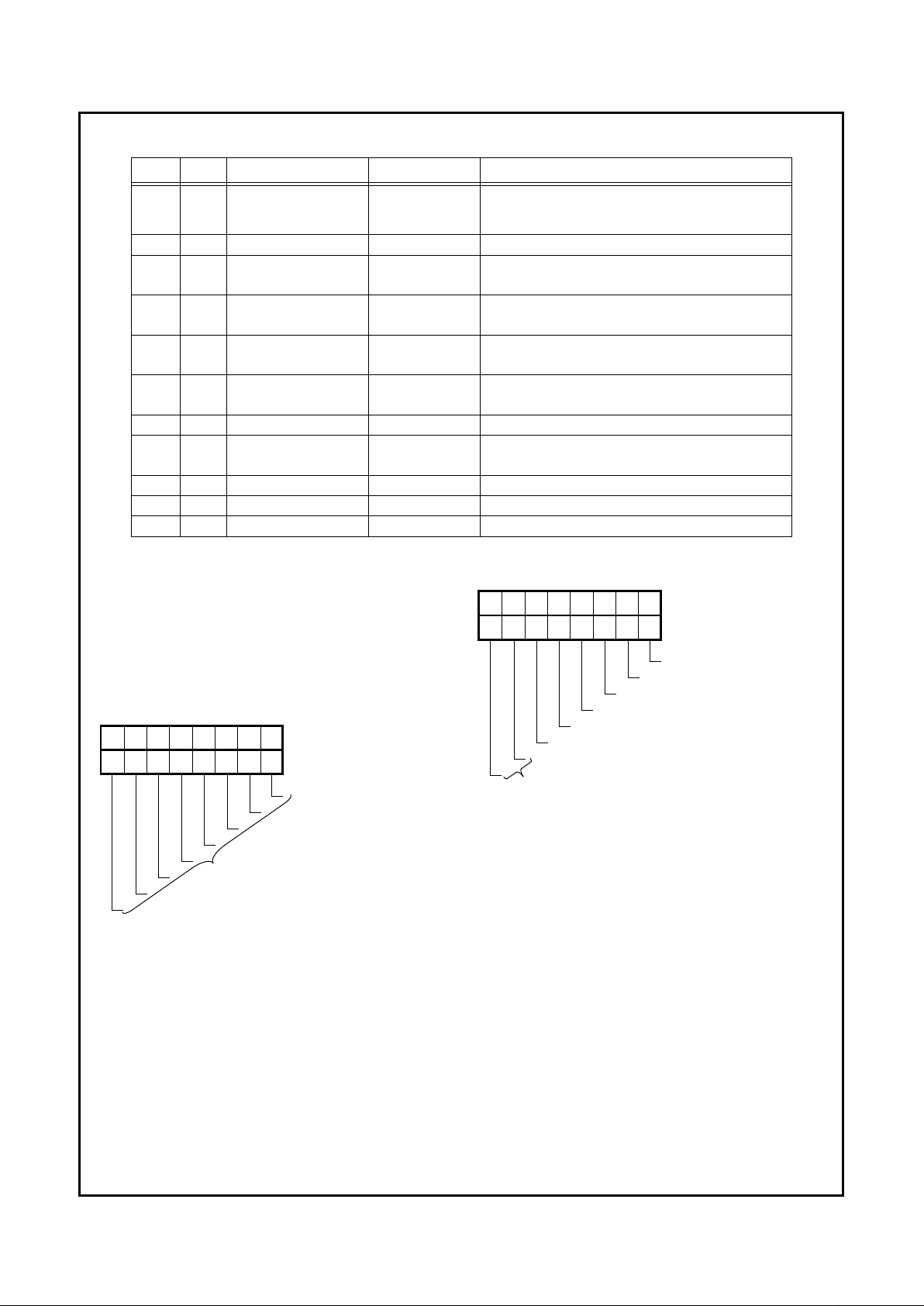
Configuration
28
CARD CONTROL REGISTERS
www.national.com
TABLE 2-17. KBC Configuration Registers for Keyboard - Logical Device 6
2.4 CARD CONTROL REGISTERS
This section describes the registers at first level indexes in
the range 20h - 2Fh.
2.4.1 SID Register
This read-only register contains the identity number of the
chip. The PC87309VLJ is identified by the value E0h in this
register.
2.4.2 SuperI/O Configuration 1 Register (SIOCF1)
This register can be read or written. It is reset by hardware
according to the BADDRs and the CFG0 strap pins see TABLE 2-1 "Strap Pins and Base Addresses" on page 20.
Bit 1,0 - BADDR1 and BADDR0
Initialized on reset by BADDR1 and BADDR0 strap pins
(BADDR0 on bit 0). These bits select the addresses of
the configuration Index and Data registers and the PnP
ISA Serial Identifier. See TABLE 2-1 "Strap Pins and
Base Addresses" on page 20.
Bit 2 - PC-AT or PS/2 Drive Mode Select
0: PS/2 drive mode.
1: PC-AT drive mode. (Default)
Bit 3 - CFG0 Bit
Initialized on reset by CFG0 strap pin. This read-only bit
selects between Full-IR and Two-UART modes.
0: Full-IR mode.
1: Two-UART mode.
Index R/W Hard Reset Soft Reset Configuration Register or Action
30h R/W 01h No Effect Activate.
See also FER1 of Power Management device
(Logical Device 4).
31h R/W 00h No Effect I/O Range Check.
60h R/W 00h No Effect Base Address MSB Register.
Bits 7-3 (for A15-11) are read only, 00000b.
61h R/W 60h No Effect Base Address LSB Register.
Bits 2-0 are read only 000b.
62h R/W 00h No Effect Command Base Address MSB Register.
Bits 7-3 (for A15-11) are read only, 00000b.
63h R/W 64h No Effect Command Base Address LSB.
Bits 2-0 are read only 100b.
70h R/W 01h No Effect KBC Interr upt (KBC IRQ1 pin) Select.
71h RW 02h No Effect KBC Interrupt Type.
Bits 1,0 are read/write; others are read only.
74h R 04h No Effect Repor t no DMA assignment.
75h R 04h No Effect Repor t no DMA assignment.
F0h R/W See Section 2.9. No Effect SuperI/O KBC Configuration Register.
76543210
Reset
Required
00000111
00000111
SID
Index 20h
Register,
Chip ID
General Purpose Scratch Bits
76543210
Reset
Required
xx1x0000
SuperI/O Configuration 1
Index 21h
BADDR0
PC-AT or PS/2 Drive Mode Select
BADDR1
CFG0
Lock Scratch Bit
KBC-Lock
Register (SIOCF1),
Page 29
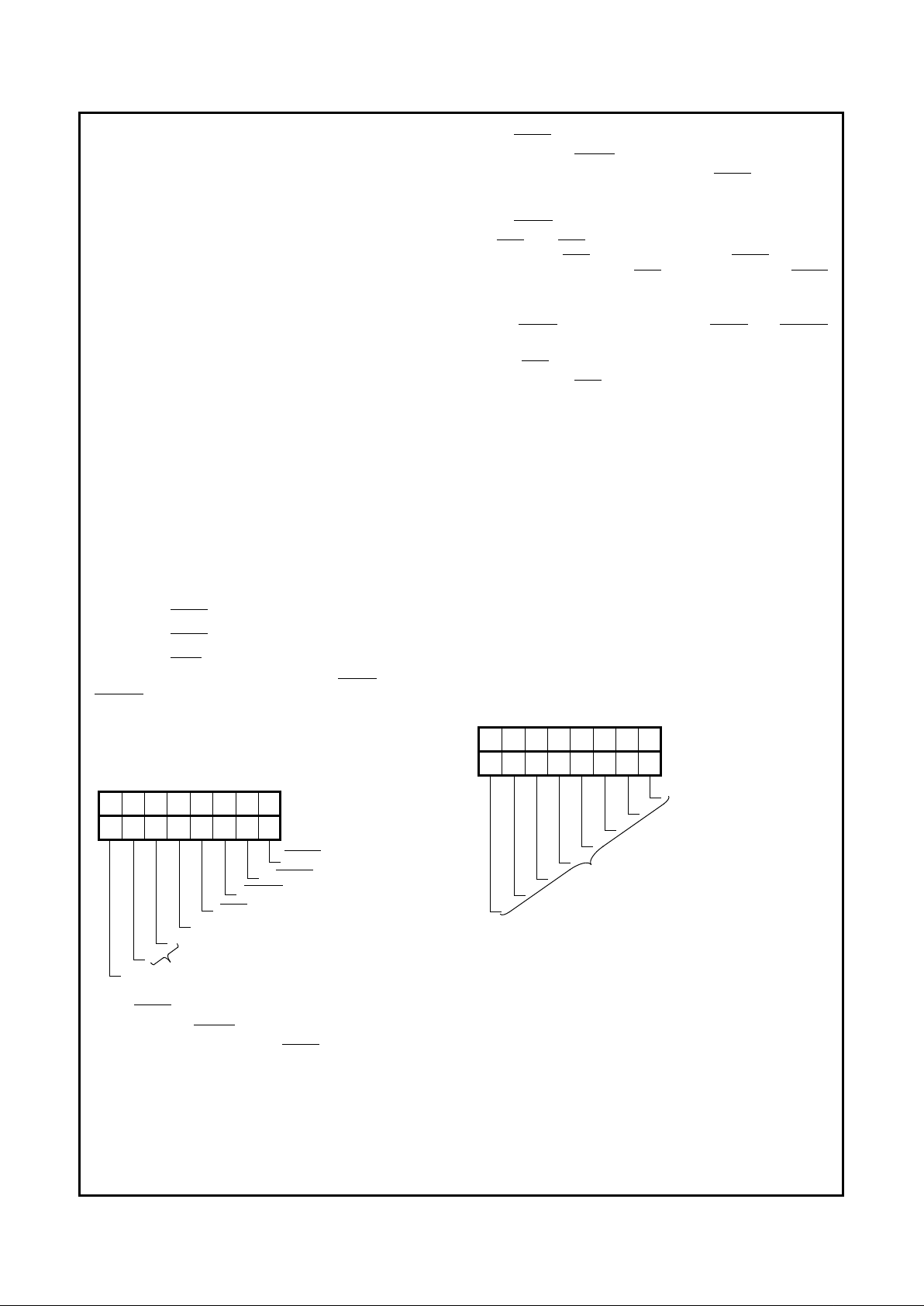
Configuration
CARD CONTROL REGISTERS
29
www.national.com
Bit 4 - KBC-Lock
This bit Locks the access to the configuration registers
of the KBC, Logical Device 6.
0: Access is enabled.
1: Access is disabled. Writes are ignored and reads
returns 0 upon access to Logical Device 6.
Bit 5 - Lock Scratch Bit
This bit controls bits 7 and 6 of this register. Once this
bit is set to 1 by software, it can be cleared to 0 only by
a hardware reset.
0: Bits 7 and 6 of this register are read/write bits.
1: Bits 7 and 6 of this register are read only bits.
Bits 7,6 - General Purpose Scratch Bits
When bit 5 is set to 1, these bits are read only. After reset they can be read or written. Once changed to readonly, they can be changed back to be read/write bits
only by a hardware reset.
2.4.3 SuperI/O Configuration 2 Register (SIOCF2)
This is a read/write register in Two-UART mode only. (In
Full-IR mode, it is a read only 00h register and cannot be
modified.) It controls the function multiplexing of the following pins:
●
Pin 43 - IRRX/P12/DRATE0
●
Pin 44 - IRTX/DENSEL
●
Pin 45 - MTR0/DRATE0
●
Pin 46 - MTR1/P12
●
Pin 48 - DR1/DENSEL
In addition, it controls the function of
DR0,1 pins when
MTR0,1 are de-selected.
Configuring the same function by software on more than
one pin is illegal, and may cause unpredictable results.
Bit 0 -
MTR0/DRATE0 Select
0: Pin 45 is
MTR0
1: Pin 45 is DRATE0 (with
MTR0 DC characteristics)
Bit 1 - MTR1/P12 Select
0: Pin 46 is
MTR1
1: Pin 46 is P12 (open drain with
MTR1 current sink
characteristics)
Bit 2 -
DR0,1 Function
DR0 and DR1 function in a single, motor-drive-select
operation.
DR0 is affected only when MTR0 is de-se-
lected (bit 0 is set to 1);
DR1 is affected only whenMTR1
is de-selected (bit 1 is set to 1).
0: No change in DR0,1 function
1:
DR0,1 become a logical OR of DR0,1 and MTR0,1
when bits 0,1 are set to 1, respectively.
Bit 3 -
DR1/DENSEL Select
0: Pin 48 is
DR1
1: Pin 48 is DENSEL
Bits 5,4 - IRRX/P12/DRATE0 Select
X0:Pin 43 is IRRX1
01:Pin 43 is P12
11:Pin 43 is DRATE0
Bit 6 - IRTX/DENSEL Select
0: Pin 44 is IRTX
1: Pin 44 is DENSEL (with IRTX DC characteristics)
Bit 7 - Reserved
This is read only 0.
2.4.4 SRID Register
This read-only register contains the identity number of the
chip revision. SRID is incremented on each revision.
76543210
Reset
Required
00000000
SuperI/O Configuration 2
Index 22h
Register (SIOCF2),
MTR0/DRATE0 Select
MTR1/P12 Select
DR0,1 Function
DR1/DENSEL Select
IRRX1/P12/DRATE0 Select
IRTX/DENSEL Select
Reserved
76543210
Reset
Required
xxxxxxxx
SRID
Index 27h
Register,
Chip Revision ID
Page 30
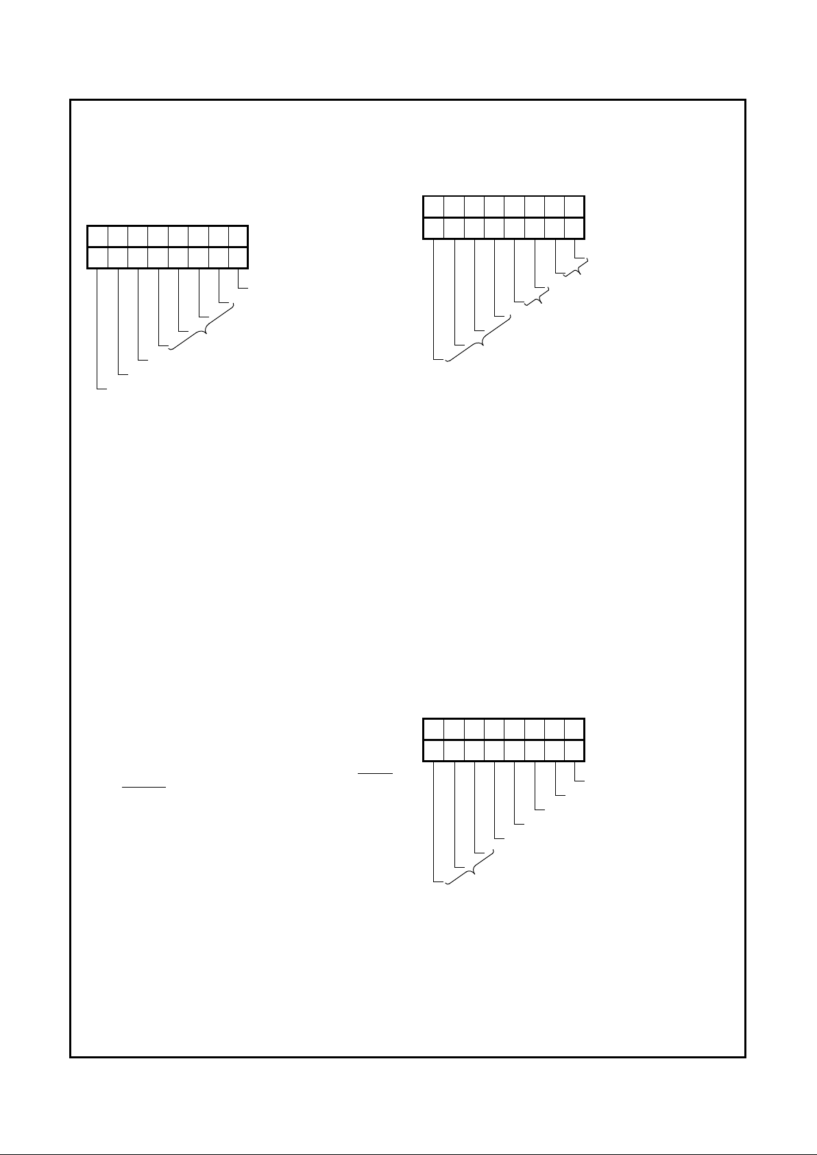
Configuration
30
FDC CONFIGURATION REGISTERS (LOGICAL DEVICE 0)
www.national.com
2.5 FDC CONFIGURATION REGISTERS (LOGICAL
DEVICE 0)
2.5.1 SuperI/O FDC Configuration Register
This read/write register is reset by hardware to 20h.
Bit 0 - TRI-STATEControl
When set, this bit causes the FDC pins to be in TRISTA TE(except the IRQ and DMA pins) when the FDC is
inactive (disabled).
This bit is ORed with a bit of PMC1 register of Logical
Device 4.
0: FDC pins are not put in TRI-STATE.
1: FDC pins are put in TRI-STATE.
Bits 4-1 - Reserved
Bit 5 - DENSEL Polarity Control
0: DENSEL is active low for 500 Kbps or 1 Mbps data
rates.
1: DENSEL is active high for 500 Kbps or 1 Mbps
data rates. (Default)
Bit 6 - TDR Register Mode
0: PC-AT Compatible drive mode (bits 7 through 2 of
TDR are not driven).
1: Enhanced dr ive mode (bits 7 through 2 of TDR are
driven on TDR read).
Bit 7 - Four Drive Control
0: Two floppy dr ives are directly controlled by
DR1-0,
MTR1-0.
1: Four floppy drives are controlled with the aid of an
external decoder.
2.5.2 Drive ID Register
This read/write register is reset by hardware to 00h. These
bits control bits 5 and 4 of the enhanced TDR register.
Bits 1,0 - Drive 0 ID
These bits are reflected on bits 5 and 4, respectively, of
the Tape Drive Register (TDR) of the FDC when drive 0
is accessed. See Section 3.3.4 "Tape Drive Register
(TDR)" on page 41.
Bits 3,2 - Drive 1 ID
These bits are reflected on bits 5 and 4, respectively, of
the TDR register of the FDC when drive 1 is accessed.
See Section 3.3.4 "Tape Drive Register (TDR)" on page
41.
Bits 7-4 - Reserved
2.6 SUPERI/O PARALLEL PORT CONFIGURATION
REGISTER (LOGICAL DEVICE 1)
This read/write register is reset by hardware to F2h. To
maintain compatibility with future chips, it is recommended
not to change bits 7-4 during normal operation. Before
changing from any EPP mode to another mode, initialize
bits 3-0 of CTR to 0100b. (See 4.2.4 on page 81.)
Bit 0 - TRI-STATE Control
When set, this bit causes the parallel port pins to be in
TRI-STATE(except IRQ and DMA pins) when the parallel port is inactive (disabled). This bit is ORed with a bit
of the PMC1 register of Logical Device4.
TRI-STATE Control
Four Drive Control
76543210
Reset
Required
00000100
Super I/O FDC
Index F0h
Configuration
Reserved
Register,
DENSEL Polarity Control
TDR Register Mode
Drive 0 ID
Reserved
76543210
Reset
Required
00000000
Index F1h
Drive ID Register,
Drive 1 ID
TRI-STATE Control
Parallel Port Mode Select
76543210
Reset
Required
01001111
Index F0h
Configuration Register,
Reserved
SuperI/O Parallel Port
Clock Enable
Reserved
Configuration Bits within the Parallel Port
Page 31

Configuration
SUPERI/O UART2 AND INFRARED CONFIGURATION REGISTER (LOGICAL DEVICE 2)
31
www.national.com
Bit 1 - Clock Enable
0: Parallel port clock disabled.
ECP modes and EPP timeout are not functional
when the logical device is active. Registers are
maintained.
1: Parallel port clock enabled.
All operation modes are functional when the logical
device is active. This bit is ANDed with a bit of the
PMC3 register of the Power Management device
(Logical Device4).
Bit 2,3 - Reserved
Bit 4 - Configuration Bits within the Parallel Port
0: The registers at base (address) + 403h, base +
404h and base + 405h are not accessible (reads
and writes are ignored).
1: When IEEE1284 mode is selected by bits 7
through 5, the registers at base (address) + 403h,
base + 404h and base + 405h are accessible.
This option supports run-time configuration within
the Parallel Port address space. An 8-byte (and
1024-byte) aligned base address is required to ac-
cess these registers. See Chapter 4 "Parallel Por t
(Logical Device 1)" on page 79 for details.
Bit 7-5 - Parallel Port Mode Select
Bit 5 is the LSB.
Selection of EPP 1.7 or 1.9 in ECP mode 4 is controlled
by bit 4 of the Control2 configuration register of the parallel port at offset 02h. See Section 4.5.17 "Control2
Register" on page 93.
000: SPP Compatible mode. PD7-0 are always output
signals.
001: SPP Extended mode. PD7-0 direction controlled
by software.
010:EPP 1.7 mode.
011:EPP 1.9 mode.
100:IEEE1284 mode (selects IEEE1284 register set),
with no support for EPP mode.
101:Reserved.
110:Reserved.
111:IEEE1284 mode (selects IEEE1284 register set),
with EPP mode selectable as mode 4.
2.7 SUPERI/O UART2 AND INFRARED
CONFIGURATION REGISTER (LOGICAL DEVICE 2)
This read/write register is reset by hardware to 02h.
Bit 0 - TRI-STATE Control for UART2 signals
This bit controls the TRI-STATE status of UART signals
(except IRQ and DMA signals) when UART2 is inactive
(disabled). This bit is ORed with a bit of the PMC1 register of the Power Management device (Logical
Device4).
0: Signals not in TRI-STATE.
1: Signals in TRI-STATE.
Bit 1 - Power Mode Control
0: Low power mode.
UART2 Clock disabled. UART2 output signals are
set to their default state. The
RI input signal can be
programmed to generate an interrupt. Registers
are maintained.
1: Normal power mode.
UART2 clock enabled. The UART2 is functional
when the logical device is active. This bit is ANDed
with a bit of the PMC3 register of the Power Management device (Logical Device 4).
Bit 2 - Busy Indicator
This read-only bit can be used by power management
software to decide when to power down UART2 logical
device. This bit is also accessed via the PMC3 register
of the Power Management device (Logical Device 4).
0: No transfer in progress.
1: Transfer in progress.
Bits 6-3 - Reserved
Bit 7 - Bank Select Enable
Enables bank switching for UART2. If this bit is cleared,
all attempts to access the extended registers are ig-
nored.
TRI-STATE Control for
Bank Select Enable
76543210
Reset
Required
01000000
Index F0h
Configuration Register,
SuperI/O UART2
Power Mode Control
Busy Indicator
Reserved
UART2 Pins
Page 32
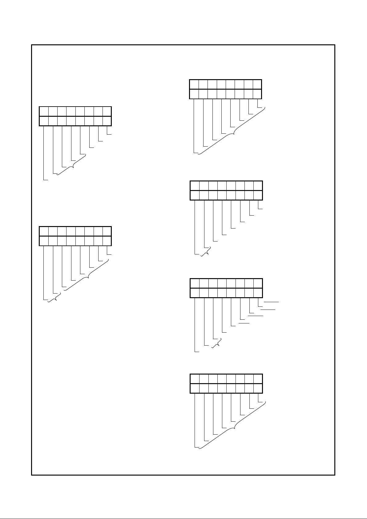
Configuration
32
SUPERI/O UART1 CONFIGURATION REGISTER (LOGICAL DEVICE 3)
www.national.com
2.8 SUPERI/O UART1 CONFIGURATION REGISTER
(LOGICAL DEVICE 3)
This read/write register is reset by hardware to 02h. Its bits
function like the bits in the SuperI/O UART2 Configuration
register
2.9 SUPERI/O KBC CONFIGURATION REGISTER
(LOGICAL DEVICE 6)
This read/write register is reset by hardware to 40h.
Bit 0 - TRI-STATE Control
When set, it causes the KBC pins (including the mouse
clock and mouse data, but excluding DMA and IRQ), to be
in TRI-STATE when the KBC is inactive (disabled).
Bits 5-1 - Reserved
Bits 7,6 - KBC Clock Source
Bit 6 is the LSB. The clock source can be changed only
when the KBC is inactive (disabled).
00:8 MHz
01:12 MHz
10:16 MHz.
11:Reserved.
2.10 CONFIGURATION REGISTER BITMAPS
TRI-STATE Control for
Bank Select Enable
76543210
Reset
Required
01000000
Index F0h
Configuration Register,
SuperI/O UART1
Power Mode Control
Busy Indicator
Reserved
UART1 Pins
Reserved
KBC Clock Source
76543210
Reset
Required
00000010
SuperI/O KBC
Index F0h
Configuration
Register,
TRI-STATE Control
76543210
Reset
Required
00000111
00000111
SID
Index 20h
Register,
Chip ID
General Purpose Scratch Bits
76543210
Reset
Required
0x10x000
SuperI/O Configuration 1
Index 21h
BADDR0
PC-AT or PS/2 Drive Mode Select
BADDR1
CFG0
Lock Scratch Bit
KBC-Lock
Register (SIOCF1),
76543210
Reset
Required
00000000
SuperI/O Configuration 2
Index 22h
Register (SIOCF2),
MTR0/DRATE0 Select
MTR1/P12 Select
DR0,1 Function
DR1/DENSEL Select
IRRX1/P12/DRATE0 Select
IRTX/DENSEL Select
Reserved
76543210
Reset
Required
xxxxxxxx
SRID
Index 27h
Register,
Chip Revision ID
Page 33

Configuration
CONFIGURATION REGISTER BITMAPS
33
www.national.com
Reserved
KBC Clock Source
76543210
Reset
Required
00000010
SuperI/O KBC
Index F0h
Configuration
Register,
TRI-STATE Control
TRI-STATE Control
Four Drive Control
76543210
Reset
Required
00000100
Super I/O FDC
Index F0h
Configuration
Reserved
Register,
DENSEL Polarity Control
TDR Register Mode
Drive 0 ID
Reserved
76543210
Reset
Required
00000000
Index F1h
Drive ID Register,
Drive 1 ID
TRI-STATE Control
Parallel Port Mode Select
76543210
Reset
Required
01001111
Index F0h
Configuration Register,
Reserved
SuperI/O Parallel Port
Clock Enable
Reserved
Configuration Bits within the Parallel Port
TRI-STATE Control for
Bank Select Enable
76543210
Reset
Required
00000000
Index F0h
Configuration Register,
SuperI/O UART1,2
Power Mode Control
Busy Indicator
Reserved
UART Pins
Page 34

The Floppy Disk Controller (FDC) (Logical Device 0)
34
3.0 The Floppy Disk Controller (FDC) (Logical Device 0)
www.national.com
3.0 The Floppy Disk Controller (FDC)
(Logical Device 0)
The Floppy Disk Controller (FDC) is suitable for all PC-AT,
EISA, PS/2, and general purpose applications. DP8473 and
N82077 software compatibility is provided. Key features include a 16-byte FIFO, PS/2 diagnostic register support, perpendicular recording mode, CMOS disk input and output
logic, and a high performance Digital Data Separator (DDS).
Figure 3-1 shows a functional block diagram of the FDC.
The rest of this chapter describes the FDC functions, data
transfer, the FDC registers, the phases of FDC commands,
the result phase status registers and the FDC commands,
in that order.
3.1 FDC FUNCTIONS
FDC functions are enabled when the FDC Function Enable
bit (bit 3) of the Function Enable Register 1 (FER1) at offset
00h in logical device 8 is set to 1. See Section 7.2.3 on page
155.
The PC87309 is software compatible with the DP8473 and
82077 Floppy Disk Controllers. Upon a power-on reset, the
16-byte FIFO is disabled. Also, the disk interface output signals are configured as active push-pull output signals,
which are compatible with both CMOS input signals and
open-collector resistor terminated disk drive input signals.
The FIFO can be enabled with the CONFIGURE command.
The FIFO can be very useful at high data rates, with systems that have a long DMA bus latency, or with multi-tasking systems such as the EISA or MCA bus structures.
The FDC supports all the DP8473 MODE command features as well as some additional features. These include
control over the enabling of the FIFO for read and write operations, disabling burst mode for the FIFO, a bit that will
configure the disk interface outputs as open-drain output
signals, and programmability of the DENSEL output signal.
DRATE0 and DENSEL pins are not available in the default
configuration of Two-UART mode. You may optionally select them on other FDC pins or on IR pins. When working
with no DRATE0 or DENSEL, you must set the BIOS and
the floppy drive to support this operation.
3.1.1 Microprocessor Interface
The Floppy Disk Controller (FDC) receives commands,
transfers data, and returns status information via an FDC
microprocessor interface. This interface consists of the
A9-3, AEN,
RD, and WR signals, which access the chip for
read and write operations; the data signals D7-0; the address lines A2-0, which select the appropriate register (see
TABLE 3-1 on page 38) an IRQ signal, and the DMA interface signals DRQ,
DACK, and TC.
3.1.2 System Operation Modes
The FDC operates in PC-AT or PS/2 drive mode, depending
on the value of bit 2 of the SuperI/O Configuration 1 register
at index 21h. See Section 2.4.2 on page 28.
FIGURE 3-1. FDC Functional Block Diagram
To Floppy Disk Interface Cable
Internal Control and Data Bus
Interface
Logic
Address
Decoder
DMA
Enable
Logic
Main Status
Register
16-Byte
FIFO
(MSR)
PC8477B
Micro-Engine
and
Timing/Control
Logic
Data Rate
Selection
Register
(DSR)
Configuration
Control
Register
(CCR)
2 KB x 16
Micro-Code
Status
Register A
Status
Register B
Digital Input
Register
(DIR)
Digital Output
Register
(DOR)
Write
Precompen-
Digital
Data
Separator
(DDS)
Disk
Input
and
Output
Logic
DRATE0
DENSEL
DIR
DR1
HDSEL
MTR0
sator
MTR1
STEP
WGATE
WDATA
DSKCHG
INDEX
RDATA
TRK0
WP
RD
FDC Chip
WR
A2-0
Reset
D7-0
FDC DMA
TC
FDC DMA
Interrupt
FDC Clock
Select
Acknowledge
Request
DR0
Page 35

The Floppy Disk Controller (FDC) (Logical Device 0)
DATA TRANSFER
35
www.national.com
PC-AT Drive Mode
The PC-AT register set is enabled. The DMA enable bit in
the Digital Output Register (DOR) becomes valid (the appropriate IRQ and DRQ signals can be put in TRI-STATE).
TC and DENSEL become active high signals (default to a
5.25" floppy disk drive).
PS/2 Drive Mode
This drive mode supports the PS/2 models 50/60/80 configuration and register set. The value of the DMA enable bit in
the Digital Output Register (DOR) becomes unimportant
(the IRQ and DRQ signals assigned to the FDC are always
valid). TC and DENSEL become active low signals (default
to 3.5" floppy drive).
3.2 DATA TRANSFER
3.2.1 Data Rates
The FDC supports the standard PC data rates of 250, 300
and 500 Kbps, as well as 1 Mbps. High performance tape
and floppy disk drives that are currently emerging in the PC
world, transfer data at 1 Mbps. The FDC also supports the
perpendicular recording mode, a new format used for some
high capacity disk drives at 1 Mbps.
The internal digital data separator needs no external components. It improves the window margin performance standards of the DP8473, and is compatible with the strict data
separator requirements of floppy disk drives and tape
drives.
The FDC contains write precompensation circuitry that defaults to 125 nsec for 250, 300, and 500 Kbps (41.67 nsec
at 1 Mbps). These values can be overridden in software to
disable write precompensation or to provide levels of precompensation up to 250 nsec.
The FDC has internal 24 mA data bus buffers which allow
direct connection to the system bus. The internal 40 mA totem-pole disk interface buffers are compatible with both
CMOS drive input signals and 150 resistor terminated disk
drive input signals.
3.2.2 The Data Separator
The internal data separator is a fully digital PLL. The fully
digital PLL synchronizes the raw data signal read from the
disk drive. The synchronized signal is used to separate the
encoded clock and data pulses. The data pulses are broken
down into bytes, and then sent to the microprocessor by the
controller.
The FDC supports data transfer rates of 250, 300, 500 Kbps
and 1 Mbps in Modified Frequency Modulation (MFM) format.
The FDC has a dynamic window margin and lock range performance capable of handling a wide range of floppy disk
drives. In addition, the data separator operates under a variety of conditions, including high fluctuations in the motor
speed of tape drives that are compatible with floppy disk
drives.
The dynamic window margin is the primary indicator of the
quality and performance level of the data separator. It indicates the toleration of the data separator for Motor Speed
Variation (MSV) of the drive spindle motor and bit jitter (or
window margin).
FIGURE 3-2 shows the dynamic window margin in the performance of the FDC at different data rates, generated using a FlexStar FS-540 floppy disk simulator and a
proprietary dynamic window margin test program written by
National Semiconductor.
FIGURE 3-2. PC87309 Dynamic Window Margin
Performance
The x axis measures MSV. MSV is translated directly to the
actual rate at which the data separator reads data from the
disk. In other words, a faster than nominal motor results in
a higher data rate.
The dynamic window margin performance curve also indicates how much bit jitter (or window margin) can be tolerated by the data separator. This parameter is shown on the yaxis of the graph. Bit jitter is caused by the magnetic interaction of adjacent data pulses on the disk, which effectively
shifts the bits away from their nominal positions in the middle of the bit window. Window margin is commonly measured as a percentage. This percentage indicates how far a
data bit can be shifted early or late with respect to its nominal bit position, and still be read correctly by the data separator. If the data separator cannot correctly decode a shifted
bit, then the data is misread and a CRC error results.
The dynamic window margin performance curve supplies
two pieces of information:
●
The maximum range of MSV (also called “lock range”)
that the data separator can handle with no read errors.
●
The maximum percentage of window margin (or bit jitter)
that the data separator can handle with no read errors.
Thus, the area under the dynamic window margin curves in
FIGURE 3-2 is the range of MSV and bit jitter that the FDC
can handle with no read errors. The internal digital data separator of the FDC performs much better than comparable
digital data separator designs, and does not require any external components.
-14-12-10 -8 -6 -4 -2 0 2 4 4 8 10 12 14
10
20
30
40
60
70
80
50
Window Margin Percentage
Motor Speed Variation (% of Nominal)
250,300, 500 Kbps and 1 Mbps
Typical Performance at 500 Kbps,
V
DD
= 5.0 V, 25˚ C
Page 36

The Floppy Disk Controller (FDC) (Logical Device 0)
36
DATA TRANSFER
www.national.com
The controller maximizes the internal digital data separator
by implementing a read algorithm that enhances the lock
characteristics of the fully digital Phase-Locked Loop (PLL).
The algorithm minimizes the effect of bad data on the synchronization between the PLL and the data.
It does this by forcing the fully digital PLL to re-lock to the
clock reference frequency any time the data separator attempts to lock to a non-preamble pattern. See the state diagram of this read algorithm in FIGURE 3-3.
FIGURE 3-3. Read Algorithm State Diagram
3.2.3 Perpendicular Recording Mode Support
The FDC is fully compatible with perpendicular recording
mode disk drives at all data transfer rates. These perpendicular drives are also called 4 Mbyte (unformatted) or 2.88
Mbyte (formatted) drives. This refers to their maximum storage capacity.
Perpendicular recording orients the magnetic flux changes
(which represent bits) vertically on the disk surface, allowing for a higher recording density than conventional longitudinal recording methods. This increased recording density
increases data rate by up to 1 Mbps, thereby doubling the
storage capacity. In addition, the perpendicular 2.88 MB
drive is read/write compatible with 1.44 MB and 720 KB diskettes (500 Kbps and 250 Kbps respectively).
The 2.88 MB drive has unique format and write data timing
requirements due to its read/write head and pre-erase head
design. This is illustrated in FIGURE 3-4.
Unlike conventional disk drives which have only a
read/write head, the 2.88 MB drive has both a pre-erase
head and read/write head. With conventional disk drives,
the read/write head, itself, can rewrite the disk without problems. 2.88 MB drives need a pre-erase head to erase the
magnetic flux on the disk surface before the read/write head
can write to the disk surface. The pre-erase head is activated during disk write operations only, i.e. FORMAT and
WRITE DATA commands.
In 2.88 MB drives, the pre-erase head leads the read/write
head by 200 µm, which translates to 38 bytes at 1 Mbps (19
bytes at 500 Kbps).
FIGURE 3-4. Perpendicular Recording Drive
Read/Write Head and Pre-Erase Head
For both conventional and perpendicular drives,
WGATE is
asserted with respect to the position of the read/write head.
With conventional drives, this means that
WGATE is asserted when the read/write head is located at the beginning of
the preamble to the data field.
With 2.88 MB drives, since the preamble must be erased
before it is rewritten,
WGATE should be asserted when the
pre-erase head is located at the beginning of the preamble
to the data field. This means that
WGATE should be asserted when the read/write head is at least 38 bytes (at 1 Mbps)
before the preamble. TABLES 3-14 on page 63 and 3-15 on
page 63 show how the perpendicular format affects gap 2
and, consequently,
WGATE timing, for different data rates.
Because of the 38-byte spacing between the read/write
head and the pre-erase head at 1 Mbps, the gap 2 length of
22 bytes used in the standard IBM disk format is not long
enough. The format standard for 2.88 MB drives at 1 Mbps
called the Perpendicular Format, increases the length of
gap 2 to 41 bytes. See FIGURE 3-5 on page 59.
The PERPENDICULAR MODE command puts the Floppy
Disk Controller (FDC) into perpendicular recording mode,
which allows it to read and write perpendicular media. Once
this command is invoked, the read, write and format commands can be executed in the normal manner. The perpendicular mode of the FDC functions at all data rates,
adjusting format and write data parameters accordingly.
See Section 3.7.9 on page 62 for more details.
3.2.4 Data Rate Selection
The FDC sets the data rate in two ways. For PC compatible
software, the Configuration Control Register (CCR) at offset
07h programs the data rate for the FDC. The lower bits D1
and D0 in the CCR set the data rate. The other bits should
be set to zero. TABLE 3-5 on page 43 shows how to encode
the desired data rate.
The lower two bits of the Data rate Select Register (DSR) at
offset 04h can also set the data rate. These bits are encoded like the corresponding bits in the CCR. The remainder of
the bits in the DSR have other functions. See the description of the DSR in Section 3.3.6 on page 43 for more details.
The data rate is determined by the last value written to either the CCR or the DSR. Either the CCR or the DSR can
override the data rate selection of the other register. When
the data rate is selected, the micro-engine and data separator clocks are scaled appropriately.
Not
sixth bit.
Read Gate = 1
Read Gate = 0
PLL
to data.
Wait six bits.
Three address
Wait for
is not a
bit.
Bit is
preamble.
Bit is not
preamble.
Three address
marks found.
Check for
three address
mark bytes.
Not third
address mark.
PLL idle
locked
to clock.
Operation
completed.
Read ID
field or
data field.
locking
first bit that
preamble
marks not found.
200 µm
(38 bytes @ 1 Mbps)
End of
ID Field
Data Field
Preamble
Intersector
Read/
PreHead
Head
Write
Gap 2
= 41 x 4Eh
Erase
Page 37

The Floppy Disk Controller (FDC) (Logical Device 0)
THE REGISTERS OF THE FDC
37
www.national.com
3.2.5 Write Precompensation
Write precompensation enables the
WDATA output signal
to adjust for the effects of bit shift on the data as it is written
to the disk surface.
Bit shift is caused by the magnetic interaction of data bits as
they are written to the disk surface. It shifts these data bits
away from their nominal position in the serial MFM data pattern. Bit shift makes it much harder for a data separator to
read data and can cause soft read errors.
Write precompensation predicts where bit shift could occur
within a data pattern. It then shifts the individual data bits
early, late, or not at all so that when they are written to the
disk, the shifted data bits are back in their nominal position.
The FDC supports software programmable write precompensation. Upon power up, the default write precompensation values shown in TABLE 3-7 on page 43, are used. In
addition, the default starting track number for write precompensation is track zero
You can use the DSR to change the write precompensation
using any of the values in TABLE 3-6 on page 43. Also, the
CONFIGURE command can change the starting track number for write precompensation.
3.2.6 FDC Low-Power Mode Logic
The FDC of the PC87309 supports two low-power modes,
manual and automatic.
In low-power mode, the micro-code is driven from the clock.
Therefore, it is disabled while the clock is off. Upon entering
the power-down state, bit 7, the RQM (Request For Master)
bit, in the Main Status Register (MSR) of the FDC is cleared
to 0.
For details about entering and exiting low-power mode by
setting bit 6 of the Data rate Select Register (DSR) or by executing the LOW PWR option of the FDC MODE command,
see Recovery from Low-Power Mode later in this section,
Section 3.3.6 on page 43 and Section 3.7.7 on page 60.
The DSR, Digital Output Register (DOR), and the Configuration Control Register (CCR) are unaffected and remain
active in power-down mode. Therefore, you should make
sure that the motor and drive select signals are turned off.
If the power to an external clock driving the PC87309 will be
independently removed while the FDC is in power-down
mode, it must not be done until 2 msec after the LOW PWR
option of the FDC MODE command is issued.
Manual Low-Power Mode
Manual low power is enabled by writing a 1 to bit 6 of the
DSR. The chip will power down immediately. This bit will be
cleared to 0 after power up.
Manual low power can also be triggered by the MODE command. Manual low power mode functions as a logical OR
function between the DSR low power bit and the LOW PWR
option of the MODE command.
Automatic Low-Power Mode
Automatic low-power mode switches the controller to low
power 500 msec (at the 500 Kbps MFM data rate) after it
has entered the Idle state. Once automatic low-power mode
is set, it does not have to be set again, and the controller automatically goes into low-power mode after entering the Idle
state.
Automatic low-power mode can only be set with the LOW
PWR option of the MODE command.
Recovery from Low-Power Mode
There are two ways the FDC section can recover from the
power-down state.
Power up is triggered by a software reset via the DOR or
DSR. Since a software reset requires initialization of the
controller, this method might be undesirable.
Power up is also triggered by a read or write to either the
Data Register (FIFO) or Main Status Register (MSR). This
is the preferred way to power up since all internal register
values are retained. It may take a few milliseconds for the
clock to stabilize, and the microprocessor will be prevented
from issuing commands during this time through the normal
MSR protocol. That means that bit 7, the Request for Master (RQM) bit, in the MSR will be a 0 until the clock has stabilized. When the controller has completely stabilized after
power up, the RQM bit in the MSR is set to 1 and the controller can continue where it left off.
3.2.7 Reset
The FDC can be reset by hardware or software.
A hardware reset consists of pulsing the Master Reset (MR)
input signal. A hardware reset sets all of the user addressable registers and internal registers to their default values.
The SPECIFY command values are unaffected by reset, so
they must be initialized again.
The major default conditions affected by reset are:
●
FIFO disabled
●
DMA disabled
●
Implied seeks disabled
●
Drive polling enabled
A software reset can be triggered by bit 2 of the Digital Output Register (DOR) or bit 7 of the Data rate Select Register
(DSR). Bit 7 of DSR clears itself, while bit 2 of DOR does
not clear itself.
If the LOCK bit in the LOCK command was set to 1 before
the software reset, the FIFO, THRESH, and PRETRK parameters in the CONFIGURE command will be retained. In
addition, the FWR, FRD, and BST parameters in the MODE
command will be retained if LOCK is set to 1. This function
eliminates the need for total initialization of the controller after a software reset.
After a hardware (assuming the FDC is enabled in the FER)
or software reset, the Main Status Register (MSR) is immediately available for read access by the microprocessor. It
will return a 00h value until all the internal registers have
been updated and the data separator is stabilized.
When the controller is ready to receive a command byte, the
MSR returns a value of 80h (Request for Master (RQM, bit
7) bit is set). The MSR is guaranteed to return the 80h value
within 250 µsec after a hardware or software reset.
All other user addressable registers other than the Main
Status Register (MSR) and Data Register (FIFO) can be accessed at any time, even during software reset.
3.3 THE REGISTERS OF THE FDC
The FDC registers are mapped to the offset address shown
in TABLE 3-1 on page 38, with the base address range provided by the on-chip address decoder. For PC-AT or PS/2
applications, the offset address range of the diskette controller is 00h through 07h from the index of logical device 0.
Page 38

The Floppy Disk Controller (FDC) (Logical Device 0)
38
THE REGISTERS OF THE FDC
www.national.com
TABLE 3-1. The FDC Registers and Addresses
The FDC supports two system operation modes: PC-AT
drive mode and PS/2 drive mode (MicroChannel systems).
Section 3.1.2 on page 34 describes each mode and “Bit 2 PC-AT or PS/2 Drive Mode Select” on page 28 describes
how each is enabled.
Unless specifically indicated otherwise, all fields in all registers are valid in both drive modes.
The FDC supports plug and play, as follows:
●
The FDC interrupt can be routed on one of the following
ISA interrupts: IRQ3-IRQ7, IRQ9-IRQ12 and IRQ15
(see PNP2 register).
●
The FDC DMA signals can be routed to one of three 8bit ISA DMA channels (see PNP2 register); and its base
address is software configurable (see FBAL and FBAH
registers).
●
Upon reset, the DMA of the FDC is routed to the DRQ2
and
DACK2 pins.
3.3.1 Status Register A (SRA)
Status Register A (SRA) monitors the state of assigned IRQ
signal and some of the disk interface signals. SRA is a readonly register that is valid only in PS/2 drive mode.
SRA can be read at any time while PS/2 drive mode is active. In PC-AT drive mode, all bits are in TRI-STATE during
a microprocessor read.
Bit 0 - Head Direction
This bit indicates the direction of the head of the Floppy
Disk Drive (FDD). Its value is the inverse of the value of
the
DIR interface output signal.
0:
DIR is not active, i.e., the head of the FDD steps
outward. (Default)
1:
DIR is active , i.e., the head of the FDD steps inw ard.
Bit 1 - Write Protect (
WP)
This bit indicates whether or not the selected Floppy
Disk Drive (FDD) is write protected. Its value reflects the
status of the
WP disk interface input signal.
0:
WP is active, i.e., the FDD in the selected drive is
write protected.
1:
WP is not active, i.e., the FDD in the selected drive
is not write protected.
Bit 2 - Beginning of Track (
INDEX)
This bit indicates the beginning of a track. Its value reflects the status of the
INDEX disk interface input signal.
0:
INDEX is active, i.e., it is the beginning of a track.
1:
INDEX is not active, i.e., it is not the beginning of a
track.
Bit 3 - Head Select
This bit indicates which side of the Floppy Disk Drive
(FDD) is selected by the head. Its value is the inverse of
the
HDSEL disk interface output signal.
0:
HDSEL is not active, i.e., the head of the FDD selects side 0. (Default)
1:
HDSEL is active, i.e., the head of the FDD selects
side 1.
Bit 4 - At Track 0 (
TRK0)
This bit indicates whether or not the head of the Floppy
Disk Drive (FDD) is at track 0. Its value reflects the status of the
TRK0 disk interface input signal.
0:
TRK0 is active , i.e., the head of the FDD is at track 0.
1:
TRK0 is not active, i.e., the head of the FDD is not
at track 0.
Bit 5 - Step
This bit indicates whether or not the head of the Floppy
Disk Drive (FDD) should move during a seek operation.
Its value is the inverse of the
STEP disk interface output
signal.
0:
STEP is not active, i.e., the head of the FDD
moves. (Default)
1:
STEP is active (low), i.e., the head of the FDD does
not move.
Bit 6 - Reserved
Bit 7 - IRQ Pending
This bit signals the completion of the execution phase of
certain FDC commands. Its value reflects the status of
the IRQ signal assigned to the FDC.
0: The IRQ signal assigned to the FDC is not active.
1: The IRQ signal assigned to the FDC is active, i.e.,
the FDD has completed execution of certain FDC
commands.
Symbol Description
Offset
R/W
A2 A1 A0
SRA Status Register A 0 0 0 R
SRB Status Register B 0 0 1 R
DOR Digital Output Register 0 1 0 R/W
TDR Tape Drive Register 0 1 1 R/W
MSR Main Status Register 1 0 0 R
DSR Data Rate Select Register 1 0 0 W
FIFO Data Register (FIFO) 1 0 1 R/W
- (Bus in TRI-STATE) 1 1 0 X
DIR Digital Input Register 1 1 1 R
CCR CCR Configuration
Control Register
111 W
76543210
Reset
Required
0000
Status Register
A (SRA)
Offset 00h
INDEX
TRK0
Step
Reserved
IRQ Pending
Head Direction
WP
Head Select
PS/2 Drive Mode
Page 39

The Floppy Disk Controller (FDC) (Logical Device 0)
THE REGISTERS OF THE FDC
39
www.national.com
3.3.2 Status Register B (SRB)
Status Register B (SRB) is a read-only diagnostic register
that is valid only in PS/2 drive mode.
SRB can be read at any time while PS/2 drive mode is active. In PC-AT drive mode, all bits are in TRI-STATE during
a microprocessor read.
Bit 0 - Motor 0 Status (MTR0)
This bit indicates the complement of the
MTR0 output
pin.
This bit is cleared to 0 by a hardware reset and unaffect-
ed by a software reset.
0:
MTR0 not active; motor 0 off (default).
1:
MTR0 active; motor 0 on.
Bit 1 - Motor 1 Status (MTR1)
This bit indicates the complement of the
MTR1 output
pin.
This bit is cleared to 0 by a hardware reset and unaffect-
ed by a software reset.
0:
MTR1 not active; motor 1 off (default).
1:
MTR1 active.; motor 1 on.
Bit 2 - Write Circuitry Status (WGATE)
This bit indicates the complement of the
WGATE output
pin.
0:
WGATE not active. The write circuitry of the selected FDD is enabled (default).
1:
WGATE active. The write circuitry of the selected
FDD is disabled.
Bit 3 - Read Data Status (RDATA)
If read data was sent, this bit indicates whether an odd
or even number of bits was sent.
Every inactive edge transition of the
RDATA disk inter-
face output signal causes this bit to change state.
0: Either no read data was sent or an even number of
bits of read data was sent. (Default)
1: An odd number of bits of read data was sent.
Bit 4 - Write Data Status (WDATA)
If write data was sent, this bit indicates whether an odd
or even number of bits was sent.
Every inactive edge transition of the
WDATA disk inter-
face output signal causes this bit to change state.
0: Either no wr ite data was sent or an even number of
bits of write data was sent. (Default)
1: An odd number of bits of write data was sent.
Bit 5 - Drive Select Status
This bit reflects the status of drive select bit 0 in the Digital Output Register (DOR). See Section 3.3.3.
It is cleared after a hardware reset and unaffected by a
software reset.
0: Either drive 0 or 2 is selected. (Default)
1: Either drive 1 or 3 is selected.
Bits 7,6 - Reserved
These bits are reserved and are always 1.
3.3.3 Digital Output Register (DOR)
DOR is a read/write register that can be written at any time.
It controls the drive select and motor enable disk interface
output signals, enables the DMA logic and contains a software reset bit.
The contents of the DOR is set to 00h after a hardware reset, and is unaffected by a software reset.
TABLE 3-2 shows how the bits of DOR select a drive and
enable a motor when the FDC is enabled (bit 3 of the Function Enable Register 1 (FER1) at offset 00h of logical device
8 is 1) and bit 7 of the SuperI/O FDC Configuration register
at index F0h is 1. Bit patterns not shown produce states that
should not be decoded to enable any drive or motor.
When the FDC is enabled and bit 7 of the of the SuperI/O
FDC Configuration register at index F0h is 1,
MTR1 pre-
sents a pulse that is the inverse of
WR. This pulse is active
whenever an I/O write to address 02h occurs. This pulse is
delayed for between 25 and 80 nsec after the leading edge
of
WR. The leading edge of this pulse can be used to clock
data into an external latch (e.g., 74LS175).
TABLE 3-2. Drive and Motor Pin Encoding for Four
Drive Configurations and Drive Exchange Support
76543210
Reset
Required
00000011
11
SRB Register
Offset 01h
WGATE
WDATA
Drive Select Status
Reserved
Reserved
MTR0
MTR1
RDATA
PS/2 Drive Mode
Digital Output
Register Bits
Control
Signals
Decoded Functions
MTR DR
765432101010
xxx1xx00-000
Activate Drive 0
and Motor 0
xx1xxx01-001
Activate Drive 1
and Motor 1
x1xxxx10-010
Activate Drive 2
and Motor 2
1xxxxx11-011
Activate Drive 3
and Motor 3
xxx0xx00-100
Activate Drive 0 and
Deactivate Motor 0
xx0xxx01-101
Activate Drive 1 and
deactivate Motor 1
x0xxxx10-110
Activate Drive 2 and
Deactivate Motor 2
0xxxxx11-111
Activate Drive 3 and
Deactivate Motor 3
Page 40

The Floppy Disk Controller (FDC) (Logical Device 0)
40
THE REGISTERS OF THE FDC
www.national.com
Usually, the motor enable and drive select output signals for
a particular drive are enabled together. TABLE 3-3 shows
the DOR hexadecimal values that enable each of the four
drives.
TABLE 3-3. Drive Enable Hexadecimal Values
The motor enable and drive select signals for drives 2 and
3 are only available when four drives are supported, i.e., bit
7 of the SuperI/O FDC Configuration register at index F0h
is 1, or when drives 2 and 0 are exchanged. These signals
require external logic.
Bits 1,0 - Drive Select
These bits select a drive, so that only one drive select
output signal is active at a time.
See “Bit 7 - Four Drive Control” on page 30 and “Bits 3,2
- Logical Drive Control (Enhanced TDR Mode Only)” on
page 41 for more information.
00:Drive 0 is selected. (Default)
01:Drive 1 is selected.
10:If four drives are supported, or drives 2 and 0 are
exchanged, drive 2 is selected.
11:If four drives are supported, drive 3 is selected.
Bit 2 - Reset Controller
This bit can cause a software reset. The controller remains in a reset state until this bit is set to 1.
A software reset affects the CONFIGURE and MODE
commands. See Sections 3.7.2 on page 55 and 3.7.7 on
page 60, respectively. A software reset does not affect
the Data rate Select Register (DSR), Configuration Control Register (CCR) and other bits of this register (DOR).
This bit must be low for at least 100 nsec. There is
enough time during consecutive writes to the DOR to reset software by toggling this bit.
0: Reset controller. (Default)
1: No reset.
Bit 3 - DMA Enable (DMAEN)
In PC-AT drive mode, this bit enables DMA operations
by controlling
DACK, TC and the appropriate DRQ and
IRQ DMA signals. In PC-AT mode, this bit is set to 0 after reset.
In PS/2 drive mode, this bit is reserved, and
DACK, TC
and the appropriate DRQ and IRQ signals are enabled.
During reset, these signals remain enabled.
0: In PC-AT drive mode, DMA operations are dis-
abled.
DACK and TC are disabled, and the appropriate DRQ and IRQ signals are put in TRI-STATE.
(Default)
1: In PC-AT drive mode, DMA operations are enabled,
i.e.,
DACK, TC and the appropriate DRQ and IRQ
signals are all enabled.
Bit 4- Motor Enable 0
If four drives are supported (bit 7 of the SuperI/O FDC
Configuration register at index F0h is 1), this bit may
control the motor output signal for drive 0, depending on
the remaining bits of this register. See TABLE 3-2 on
page 39.
If two drives are supported (bit 7 of the SuperI/O FDC
Configuration register at index F0h is 0), this bit controls
the motor output signal for drive 0.
0: The motor signal for drive 0 is not active.
1: The motor signal for drive 0 is active.
Bit 5 - Motor Enable 1
If four drives are supported (bit 7 of the SuperI/O FDC
Configuration register at index F0h is 1), this bit may
control the motor output signal for drive 0, depending on
the remaining bits of this register. See TABLE 3-2.
If two drives are supported (bit 7 of the SuperI/O FDC
Configuration register at index F0h is 0), this bit controls
the motor output signal for drive 1.
0: The motor signal for drive 1 is not active.
1: The motor signal for drive 1 is active.
Bit 6 - Motor Enable 2
If drives 2 and 0 are exchanged (see "Bits 3,2 - Logical
Drive Control (Enhanced TDR Mode Only)" on page
41), or if four drives are supported (bit 7 of the SuperI/O
FDC Configuration register at index F0h is 1), this bit
controls the motor output signal for drive 2. See TABLE
3-2.
0: The motor signal for drive 2 is not active.
1: The motor signal for drive 2 is active.
Bit 7 - Motor Enable 3
If four drives are supported (bit 7 of the SuperI/O FDC
Configuration register at index F0h is 1), this bit may
control the motor output signal for drive 3, depending on
the remaining bits of this register. See TABLE 3-2.
0: The motor signal for drive 3 is not active.
1: The motor signal for drive 3 is active.
Drive DOR Value (Hex)
01C
12D
24E
38F
76543210
Reset
Required
00000000
Digital Output
Register (DOR)
Offset 02h
Reset Controller
Motor Enable 0
Motor Enable 1
Motor Enable 2
Motor Enable 3
Drive Select
DMAEN
Page 41
The Floppy Disk Controller (FDC) (Logical Device 0)
THE REGISTERS OF THE FDC
41
www.national.com
3.3.4 Tape Drive Register (TDR)
The TDR register is a read/write register that acts as the
Floppy Disk Controller’s (FDC) drive type register.
AT Compatible
TDR Mode
In this mode, the TDR assigns a drive number to the tape
drive support mode of the data separator. All other logical
drives can be assigned as floppy drive support. Bits 7-2 are
in TRI-STATE during read operations.
Enhanced
TDR Mode
In this mode, all the bits of the TDR define operations with
Enhanced floppy disk drives.
TABLE 3-4. TDR Bit Utilization and Reset Values in Different Drive Modes
Bits 1,0 - Tape Drive Select 1,0
These bits assign a logical drive number to a tape drive.
Drive 0 is not available as a tape drive and is reserved
as the floppy disk boot drive.
00:No drive selected.
01:Drive 1 selected.
10:Drive 2 selected.
11:Drive 3 selected.
Bits 3,2 - Logical Drive Control (Enhanced TDR Mode Only)
These read/write bits control logical drive exchange between drives 0 and 2, only.
They enable software to exchange the physical floppy
disk drive and motor control signals assigned to pins.
Drive 3 is never exchanged for drive 2.
When four drives are configured, i.e., bit 7 of SuperI/O
FDC Configuration register at index F0h is 1, logical
drives are not exchanged.
00:No logical drive exchange.
01: Disk dr ive and motor control signal assignment to
pins exchanged between logical drives 0 and 1.
10: Disk dr ive and motor control signal assignment to
pins exchanged between logical drives 0 and 2.
11:Reserved. Unpredictable results when configured.
Bits 5,4 - Drive ID1,0 Information
If the value of bits 1,0 of the Digital Output Register
(DOR) are 00, these bits reflect the ID of drive 0, i.e., the
value of bits 1,0, respectively, of the Drive ID register at
index F1h. See “Bits 1,0 - Drive 0 ID” on page 30.
If the value of bits 1,0 of the Digital Output Register
(DOR) are 01, these bits reflect the ID of drive 1, i.e., the
value of bits 3,2, respectively, of the Drive ID register at
index F1h. See “Bits 3,2 - Drive 1 ID” on page 30.
Bits 7,6 - Reserved.
These bits are reserved and are read as 11b.
76543210
Reset
Required
001
Tape Drive
Register (TDR)
Offset 03h
Tape Drive Select 1,0
AT Compatible TDR Mode
TRI-STATE During Read Operations
Not Used
76543210
Reset
Required
001
Tape Drive
Register (TDR)
Offset 03h
Reserved
Reserved
Tape Drive Select 1,0
Logical Drive Exchange
Enhanced TDR Mode
Drive ID1 Information
Drive ID0 Information
TDR Mode
Bit 6 of SuperI/O
FDC Configuration
Register
Bits of TDR
Drive ID1 Drive ID0
Logical Drive
Exchange
Drive Select
543210
PC-AT
Compatible
0
Not used. Floated in TRI-STATE during read
operations.
00
Enhanced 1 1 1 0 0 0 0
Page 42

The Floppy Disk Controller (FDC) (Logical Device 0)
42
THE REGISTERS OF THE FDC
www.national.com
3.3.5 Main Status Register (MSR)
This read-only register indicates the current status of the
Floppy Disk Controller (FDC), indicates when the disk controller is ready to send or receive data through the Data
Register (FIFO) and controls the flow of data to and from the
Data Register (FIFO).
The MSR can be read at any time. It should be read before
each byte is transferred to or from the Data Register (FIFO)
except during a DMA transfer. No delay is required when
reading this register after a data transfer.
The microprocessor can read the MSR immediately after a
hardware or software reset, or recovery from a power down.
The MSR contains a value of 00h, until the FDC clock has
stabilized and the internal registers have been initialized.
When the FDC is ready to receive a new command, it reports a value of 80h for the MSR to the microprocessor.
System software can poll the MSR until the MSR is ready.
The MSR must report an 80h value (RQM set to 1) within
2.5 msec after reset or power up.
Bit 0 - Drive 0 Busy
This bit indicates whether or not drive 0 is busy.
It is set to 1 after the last byte of the command phase of
a SEEK or RECALIBRATE command is issued for drive
0.
This bit is cleared to 0 after the first byte in the result
phase of the SENSE INTERRUPT command is read for
drive 0.
0: Not busy.
1: Busy.
Bit 1 - Drive 1 Busy
This bit indicates whether or not drive 1 is busy.
It is set to 1 after the last byte of the command phase of
a SEEK or RECALIBRATE command is issued for drive
1.
This bit is cleared to 0 after the first byte in the result
phase of the SENSE INTERRUPT command is read for
drive 1.
0: Not busy.
1: Busy.
Bit 2 - Drive 2 Busy
This bit indicates whether or not drive 2 is busy.
It is set to 1 after the last byte of the command phase
of a SEEK or RECALIBRATE command is issued for
drive 2.
This bit is cleared to 0 after the first byte in the result
phase of the SENSE INTERRUPT command is read for
drive 2.
0: Not busy.
1: Busy.
Bit 3 - Drive 3 Busy
This bit indicates whether or not drive 3 is busy.
It is set to 1 after the last byte of the command phase
of a SEEK or RECALIBRATE command is issued for
drive 3.
This bit is cleared to 0 after the first byte in the result
phase of the SENSE INTERRUPT command is read for
drive 3.
0: Not busy.
1: Busy.
Bit 4 - Command in Progress
This bit indicates whether or not a command is in
progress. It is set after the first byte of the command
phase is written. This bit is cleared after the last byte of
the result phase is read.
If there is no result phase in a command, the bit is
cleared after the last byte of the command phase is
written.
0: No command is in progress.
1: A command is in progress.
Bit 5 - Non-DMA Execution
This bit indicates whether or not the controller is in the
execution phase of a byte transfer operation in nonDMA mode.
This bit is used for multiple byte transfers by the microprocessor in the execution phase through interrupts or
software polling.
0: The FDC is not in the execution phase.
1: The FDC is in the execution phase.
Bit 6 - Data I/O (Direction)
Indicates whether the controller is expecting a byte to be
written or read, to or from the Data Register (FIFO).
0: Data will be written to the FIFO.
1: Data will be read from the FIFO.
Bit 7 - Request for Master (RQM)
This bit indicates whether or not the controller is ready
to send or receive data from the microprocessor through
the Data Register (FIFO). It is cleared to 0 immediately
after a byte transfer and is set to 1 again as soon as the
disk controller is ready for the next byte.
During a Non-DMA execution phase, this bit indicates
the status of the interrupt.
0: Not ready. (Default)
1: Ready to transfer data.
76543210
Reset
Required
00000000
Main Status
Register (MSR)
Offset 04h
Drive 2 Busy
Non-DMA Execution
Data I/O Direction
RQM
Drive 1 Busy
Drive 3 Busy
Command in Progress
Drive 0 Busy
Read Operations
Page 43

The Floppy Disk Controller (FDC) (Logical Device 0)
THE REGISTERS OF THE FDC
43
www.national.com
3.3.6 Data Rate Select Register (DSR)
This write-only register is used to program the data transfer
rate, amount of write precompensation, power down mode,
and software reset.
The data transfer rate is programmed via the CCR, not the
DSR, for PC-AT, PS/2 and MicroChannel applications. Other applications can set the data transfer rate in the DSR.
The data rate of the floppy controller is determined by the
most recent write to either the DSR or CCR.
The DSR is unaffected by a software reset. A hardware reset sets the DSR to 02h, which corresponds to the default
precompensation setting and a data transfer rate of 250
Kbps.
Bits 1,0 - Data Transfer Rate Select
These bits determine the data transfer rate for the Floppy Disk Controller (FDC), depending on the supported
speeds. TABLE 3-5 shows the data transfer rate selected by each value of this field.
These bits are unaffected by a software reset, and are
set to 10 (250 Kbps) after a hardware reset.
TABLE 3-5. Data Transfer Rate Encoding
Bits 4-2 - Precompensation Delay Select
This field sets the write precompensation delay that the
Floppy Disk Controller (FDC) imposes on the
WDATA
disk interface output signal, depending on the supported
speeds. TABLE shows the delay for each value of this
field.
In most cases, the default delays shown in TABLE 3-7
are adequate. However, alternate values may be used
for specific drive and media types.
Track 0 is the default starting track number for precompensation. The starting track number can be changed
using the CONFIGURE command.
TABLE 3-6. Write Precompensation Delays
TABLE 3-7. Default Precompensation Delays
Bit 5 - Undefined
Should be set to 0.
Bit 6 - Low Power
This bit triggers a manual power down of the FDC in
which the clock and data separator circuits are turned
off. A manual power down can also be triggered by the
MODE command.
After a manual power down, the FDC returns to normal
power after a software reset, or an access to the Data
Register (FIFO) or the Main Status Register (MSR).
0: Normal power.
1: Trigger power down.
Bit 7 - Software Reset
This bit controls the same kind of software reset of the
FDC as bit 2 of the Digital Output Register (DOR). The
difference is that this bit is automatically cleared to 0 (no
reset) 100 nsec after it was set to 1.
See also “Bit 2 - Reset Controller” on page 40.
0: No reset. (Default)
1: Reset.
3.3.7 Data Register (FIFO)
The Data Register of the FDC is a read/write register that is
used to transfer all commands, data and status information
between the microprocessor and the FDC.
During the command phase, the microprocessor writes
command bytes into the Data Register after polling the
RQM (bit 7) and DIO (bit 6) bits in the MSR. During the result phase, the microprocessor reads result bytes from the
Data Register after polling the RQM and DIO bits in the
MSR.
DSR Bits
Data Transfer Rate
10
0 0 500 Kbps
0 1 300 Kbps
1 0 250 Kbps
1 1 1 Mbps
76543210
Reset
Required
01000000
Data Rate Select
Register (DSR)
Offset 04h
Precompensation Delay Select
Undefined
Low Power
Software Reset
Data Transfer Rate Select
Write Operations
DSR Bits
Duration of Delay
432
0 0 0 Default (TABLE 3-7)
0 0 1 41.7 nsec
0 1 0 83.3 nsec
0 1 1 125.0 nsec
1 0 0 166.7 nsec
1 0 1 208.3 nsec
1 1 0 250.0 nsec
1 1 1 0.0 nsec
Data Rate Precompensation Delay
1 Mbps 41.7 nsec
500 Kbps 125.0 nsec
300 Kbps 125.0 nsec
250 Kbps 125.0 nsec
Page 44

The Floppy Disk Controller (FDC) (Logical Device 0)
44
THE REGISTERS OF THE FDC
www.national.com
Use of the FIFO buffer lengthens the interrupt latency period and, thereby, reduces the chance of a disk overrun or
underrun error occurring. Typically, the FIFO buffer is used
at a 1 Mbps data transfer rate or with multi-tasking operating
systems.
Enabling and Disabling the FIFO Buffer
The 16-byte FIFO buffer can be used for DMA, interrupt, or
software polling type transfers during the execution of a
read, write, format or scan command.
The FIFO buffer is enabled and its threshold is set by the
CONFIGURE command.
When the FIFO buffer is enabled, only execution phase byte
transfers use it. If the FIFO buffer is enabled, it is not disabled after a software reset if the LOCK bit is set in the
LOCK command.
The FIFO buffer is always disabled during the command
and result phases of a controller operation. A hardware reset disables the FIFO buffer and sets its threshold to zero.
The MODE command can also disable the FIFO for read or
write operations separately.
After a hardware reset, the FIFO buffer is disabled to maintain compatibility with PC-AT systems.
Burst Mode Enabled and Disabled
The FIFO buffer can be used with burst mode enabled or
disabled by the MODE command.
In burst mode, the DRQ or IRQ signal assigned to the FDC
remains active until all of the bytes have been transferred to
or from the FIFO buffer.
When burst mode is disabled, the appropriate DRQ or IRQ
signal is deactivated for 350 nsec to allow higher priority
transfer requests to be processed.
FIFO Buffer Response Time
During the execution phase of a command involving data
transfer to or from the FIFO buffer, the maximum time the
system has to respond to a data transfer service request is
calculated by the following formula:
Max_Time = (THRESH + 1) x 8 x t
DRP
– (16 x t
ICP
)
This formula applies for all data transfer rates, whether the
FIFO buffer is enabled or disabled. THRESH is a 4-bit value
programmed by the CONFIGURE command, which sets
the threshold of the FIFO buffer. If the FIFO buffer is disabled, THRESH is zero in the above formula. The last term
in the formula, (16 x t
ICP
) is an inherent delay due to the microcode overhead required by the FDC. This delay is also
data rate dependent. Section 10.3.14 on page 183 specifies
minimum and maximum values for t
DRP
and t
ICP
.
The programmable FIFO threshold (THRESH) is useful in
adjusting the FDC to the speed of the system. A slow system with a sluggish DMA transfer capability requires a high
value for THRESH. this gives the system more time to respond to a data transfer service request (DRQ for DMA
mode or IRQ for interrupt mode). Conversely, a fast system
with quick response to a data transfer service request can
use a low value for THRESH.
3.3.8 Digital Input Register (DIR)
This read-only diagnostic register is used to detect the state
of the
DSKCHG disk interface input signal and some diag-
nostic signals. DIR is unaffected by a software reset.
The bits of the DIR register function differently depending
on whether the FDC is operating in PC-AT drive mode or in
PS/2 drive mode. See Section 3.1.2 on page 34.
In PC-AT drive mode, bits 6 through 0 are in TRI-STATE to
prevent conflict with the status register of the hard disk at
the same address as the DIR.
Bit 0 - High Density (PS/2 Drive Mode Only)
In PC-AT drive mode, this bit is reserved, in TRI-STATE
and used by the status register of the hard disk.
In PS/2 drive mode, this bit indicates whether the data
transfer rate is high or low.
0: The data transfer rate is high, i.e., 1 Mbps or 500 Kbps .
76543210
Reset
Required
Data Register
(FIFO)
Offset 05h
Data
76543210
Reset
Required
11111
Digital Input
Register (DIR)
Offset 07h
DSKCHG
Reserved, In TRI-STATE
Read Operations, PC-AT Drive Mode
76543210
Reset
Required
11111
Digital Input
Register (DIR)
Offset 07h
DRATE1 Status
DSKCHG
DRATE0 Status
Reserved
High Density
Read Operations, PS/2 Drive Mode
Page 45

The Floppy Disk Controller (FDC) (Logical Device 0)
THE PHASES OF FDC COMMANDS
45
www.national.com
1: The data transfer rate is low, i.e., 300 Kbps or 250 Kbps.
Bits 2,1 - Data Rate Select 1,0 (DRATE1,0)
(PS/2 Drive Mode Only)
In PC-AT drive mode, these bits are reserved, in TRISTATE and used by the status register of the hard disk.
In PS/2 drive mode, these bits indicate the status of the
DRATE1,0 bits programmed in DSR or CCR, whichever
is written last.
The significance of each value for these bits depends on
the supported speeds. See TABLE 3-5 on page 43.
00:Data transfer rate is 500 Kbps.
01:Data transfer rate is 300 Kbps.
10:Data transfer rate is 250 Kbps.
11:Data transfer rate is 1 Mbps.
Bits 6-3 - Reserved
These bits are reserved and are always 1. In PC-AT
mode these bits are also in TRI-STATE. They are used
by the status register of the fixed hard disk.
Bit 7 - Disk Changed (
DSKCHG)
This bit reflects the status of the
DSKCHG disk interface
input signal.
During power down this bit is invalid, if it is read by the
software.
0:
DSKCHG is not active.
1:
DSKCHG is active.
3.3.9 Configuration Control Register (CCR)
This write-only register can be used to set the data transfer
rate (in place of the DSR) for PC-AT, PS/2 and MicroChannel applications. Other applications can set the data transfer rate in the DSR. See Section 3.3.6 on page 43.
This register is not affected by a software reset.
The data rate of the floppy controller is determined by the
last write to either the CCR register or to the DSR register.
Bits 1,0 - Data Transfer Rate Select 1,0 (DRATE 1,0)
These bits determine the data transfer rate for the Floppy Disk Controller (FDC), depending on the supported
speeds.
TABLE 3-5 on page 43 shows the data transfer rate selected by each value of this field.
These bits are unaffected by a software reset, and are
set to 10 (250 Kbps) after a hardware reset.
Bits 7-2 - Reserved
These bits should be set to 0.
3.4 THE PHASES OF FDC COMMANDS
FDC commands may be in the command phase, the execution phase or the result phase. The active phase determines
how data is transferred between the Floppy Disk Controller
(FDC) and the host microprocessor. When no command is
in progress, the FDC may be either idle or polling a drive.
3.4.1 Command Phase
During the command phase, the microprocessor writes a
series of bytes to the Data Register (FIFO). The first command byte contains the opcode for the command, which the
controller can interpret to determine how many more command bytes to expect. The remaining command bytes contain the parameters required for the command.
The number of command bytes varies for each command.
All command bytes must be written in the order specified in
the Command Description Table in Section 3.7 on page 53.
The execution phase starts immediately after the last byte
in the command phase is written.
Prior to performing the command phase, the Digital Output
Register (DOR) should be set and the data rate should be
set with the Data rate Select Register (DSR) or the Configuration Control Register (CCR).
The Main Status Register (MSR) controls the flow of command bytes, and must be polled by the software before writing each command phase byte to the Data Register (FIFO).
Prior to writing a command byte, bit 7 of MSR (RQM, Request for Master) must be set and bit 6 of MSR (DIO, Data
I/O direction) must be cleared.
After the first command byte is written to the Data Register
(FIFO), bit 4 of MSR (CMD PROG, Command in Progress)
is also set and remains set until the last result phase byte is
read. If there is no result phase, the CMD PROG bit is
cleared after the last command byte is written.
A new command may be initiated after reading all the result
bytes from the previous command. If the next command requires selection of a different drive or a change in the data
rate, the DOR and DSR or CCR should be updated, accordingly. If the command is the last command, the software
should deselect the drive.
Normally, command processing by the controller core and
updating of the DOR, DSR, and CCR registers by the microprocessor are operations that can occur independently of
one another. Software must ensure that the these registers
are not updated while the controller is processing a command.
3.4.2 Execution Phase
During the execution phase, the Floppy Disk Controller
(FDC) performs the desired command.
Commands that involve data transfers (e.g., read, write and
format operations) require the microprocessor to write or
read data to or from the Data Register (FIFO) at this time.
Some commands, such as SEEK or RECALIBRATE, control the read/write head movement on the disk drive during
the execution phase via the disk interface signals. Execution of other commands does not involve any action by the
microprocessor or disk drive, and consists of an internal operation by the controller.
76543210
Reset
Required
01000000
Configuration Control
Register (CCR)
Offset 07h
Reserved
DRATE1
DRATE0
Write Operations
Page 46

The Floppy Disk Controller (FDC) (Logical Device 0)
46
THE PHASES OF FDC COMMANDS
www.national.com
Data can be transferred between the microprocessor and
the controller during execution in DMA mode, interrupt
transfer mode or software polling mode. The last two modes
are non-DMA modes. All data transfer modes work with the
FIFO enabled or disabled.
DMA mode is used if the system has a DMA controller. This
allows the microprocessor to do other tasks while data
transfer takes place during the execution phase.
If a non-DMA mode is used, an interrupt is issued for each
byte transferred during the execution phase. Also, instead
of using the interrupt during a non-DMA mode transfer, the
Main Status Register (MSR) can be polled by software to indicate when a byte transfer is required.
DMA Mode - FIFO Disabled
DMA mode is selected by writing a 0 to the DMA bit in the
SPECIFY command and by setting bit 3 of the DOR (DMA
enabled) to 1.
In the execution phase when the FIFO is disabled, each
time a byte is ready to be transferred, a DMA request (DRQ)
is generated in the execution phase. The DMA controller
should respond to the DRQ with a DMA acknowledge
(
DACK) and a read or write pulse. The DRQ is cleared by
the leading edge of the active low
DACK input signal. After
the last byte is transferred, an interrupt is generated, indicating the beginning of the result phase.
During DMA operations, FDC address signals are ignored
since AEN input signal is 1. The
DACK signal acts as the
chip select signal for the FIFO, in this case, and the state of
the address lines A2-0 is ignored. The Terminal Count (TC)
signal can be asserted by the DMA controller to terminate
the data transfer at any time. Due to internal gating, TC is
only recognized when
DACK is low.
PC-AT Drive Mode
In PC-AT drive mode when the FIFO is disabled, the con-
troller is in single byte transfer mode. That is, the system
has the time it takes to transfer one byte, to service a DMA
request (DRQ) from the controller. DRQ is deactivated between bytes.
PS/2 Drive Mode
In PS/2 drive mode, for DMA transfers with the FIFO dis-
abled, instead of single byte transfer mode, the FIFO is enabled with THRESH = 0Fh. Thus, DRQ is asserted when
one byte enters the FIFO during a read, and when one byte
can be written to the FIFO during a write. DRQ is deactivated by the leading edge of the
DACK input signal, and is as-
serted again when
DACK becomes inactive high. This
operation is very similar to burst mode transfer with the
FIFO enabled except that DRQ is deactivated between
bytes.
DMA Mode - FIFO Enabled
Read Data Transfers
Whenever the number of bytes in the FIFO is greater than
or equal to (16 − THRESH), a DRQ is generated. This is the
trigger condition for the FIFO read data transfers from the
floppy controller to the microprocessor.
When the last byte in the FIFO has been read, DRQ becomes inactive. DRQ is asserted again when the FIFO trigger condition is satisfied. After the last byte of a sector is
read from the disk, DRQ is again generated even if the FIFO
has not yet reached its threshold trigger condition. This
guarantees that all current sector bytes are read from the
FIFO before the next sector byte transfer begins.
Burst Mode Enabled - DRQ remains active until enough
bytes have been read from the controller to empty the
FIFO.
Burst Mode Disabled - DRQ is deactivated after each
read transfer. If the FIFO is not completely empty, DRQ
is asserted again after a 350 nsec delay. This allows
other higher priority DMA transfers to take place between floppy disk transfers.
In addition, this mode allows the controller to work correctly in systems where the DMA controller is put into a
read verify mode, where only
DACK signals are sent to
the FDC, with no
RD pulses. This read verify mode of
the DMA controller is used in some PC software. When
burst mode is disabled, a pulse from the
DACK input
signal may be issued by the DMA controller, to correctly
clocks data from the FIFO.
Write Data Transfers
Whenever the number of bytes in the FIFO is less than or
equal to THRESH, a DRQ is generated. This is the trigger
condition for the FIFO write data transfers from the microprocessor to the FDC.
Burst Mode Enabled - DRQ remains active until enough
bytes have been written to the controller to completely
fill the FIFO.
Burst Mode Disabled - DRQ is deactivated after each
write transfer. If the FIFO is not full, DRQ is asserted
again after a 350 nsec delay. Deactivation of DRQ allows other higher priority DMA transfers to take place
between floppy disk transfers.
The FIFO has a byte counter which monitors the number of
bytes being transferred to the FIFO during write operations
whether burst mode is enabled or disabled. When the last
byte of a sector is transferred to the FIFO, DRQ is deactivated even if the FIFO has not been completely filled. Thus,
the FIFO is cleared after each sector is written. Only after
the FDC has determined that another sector is to be written,
is DRQ asserted again. Also, since DRQ is deactivated immediately after the last byte of a sector is written to the
FIFO, the system will not be delayed by deactivation of
DRQ and is free to do other operations.
Read and Write Data Transfers
The
DACK input signal from the DMA controller may be held
active during an entire burst, or a pulse may be issued for
each byte transferred during a read or write operation. In
burst mode, the FDC deactivates DRQ as soon as it recognizes that the last byte of a burst was transferred.
If a DACK pulse is issued for each byte, the leading edge of
this pulse is used to deactivate DRQ. If a
DACK pulse is is-
sued,
RD or WR is not required. This is the case during the
read-verify mode of the DMA controller.
If
DACK is held active during the entire burst, the trailing
edge of the
RD or WR pulse is used to deactivate DRQ.
DRQ is deactivated within 50 nsec of the leading edge of
DACK, RD, or WR. This quick response should prevent the
DMA controller from transferring extra bytes in most of the
applications.
Page 47

The Floppy Disk Controller (FDC) (Logical Device 0)
THE PHASES OF FDC COMMANDS
47
www.national.com
Overrun Errors
An overrun or underrun error terminates the execution of a
command, if the system does not transfer data within the allotted data transfer time. (See Section 3.3.7 on page 43.
)
This puts the controller in the result phase.
During a read overrun, the microprocessor is required to
read the remaining bytes of the sector before the controller
asserts the appropriate IRQ signifying the end of execution.
During a write operation, an underrun error terminates the
execution phase after the controller has written the remaining bytes of the sector with the last correctly written byte to
the FIFO. Whether there is an error or not, an interrupt is
generated at the end of the execution phase, and is cleared
by reading the first result phase byte.
DACK asserted alone, without a RD or WR pulse, is also
counted as a transfer. If pulses of
RD or WR are not being
issued for each byte, a
DACK pulse must be issued for each
byte so that the Floppy Disk Controller(FDC) can count the
number of bytes correctly.
The VERIFY command, allows easy verification of data
written to the disk without actually transferring the data on
the data bus.
Interrupt Transfer Mode - FIFO Disabled
If interrupt transfer (non-DMA) mode is selected, the appropriate IRQ signal is asserted instead of DRQ, when each
byte is ready to be transferred.
The Main Status Register (MSR) should be read to verify
that the interrupt is for a data transfer. The RQM and NON
DMA bits (bits 7 and 5, respectively) in the MSR are set to
1. The interrupt is cleared when the byte is transferred to or
from the Data Register (FIFO). To transfer the data in or out
of the Data register, you must use the address bits of the
FDC together and
RD or WR must be active, i.e., A2-0 must
be valid. It is not enough to just assert the address bits of
the FDC.
RD or WR must also be active for a read or write
transfer to be recognized.
The microprocessor should transfer the byte within the data
transfer service time (see Section 3.3.7 on page 43). If the
byte is not transferred within the time allotted, an overrun error is indicated in the result phase when the command terminates at the end of the current sector.
An interrupt is also generated after the last byte is transferred. This indicates the beginning of the result phase. The
RQM and DIO bits (bits 7 and 6, respectively) in the MSR
are set to 1, and the NON DMA bit (bit 5) is cleared to 0. This
interrupt is cleared by reading the first result byte.
Interrupt Transfer Mode - FIFO Enabled
Interrupt transfer (non-DMA) mode with the FIFO enabled is
very similar to interrupt transfer mode with the FIFO disabled. In this case, the appropriate IRQ signal is asserted
instead of DRQ, under the same FIFO threshold trigger conditions.
The MSR should be read to verify that the interrupt is for a
data transfer. The RQM and non-DMA bits (bits 7 and 5, respectively) in the MSR are set. To transfer the data in or out
of the Data register, you must use the address bits of the
FDC together and
RD or WR must be active, i.e., A2-0 must
be valid. It is not enough to just assert the address bits of
the FDC.
RD or WR must also be active for a read or write
transfer to be recognized.
Burst mode may be used to hold the IRQ signal active during a burst, or burst mode may be disabled to toggle the IRQ
signal for each byte of a burst. The Main Status Register
(MSR) is always valid to the microprocessor. For example,
during a read command, after the last byte of data has been
read from the disk and placed in the FIFO, the MSR still indicates that the execution phase is active, and that data
needs to be read from the Data Register (FIFO). Only after
the last byte of data has been read by the microprocessor
from the FIFO does the result phase begin.
The overrun and underrun error procedures for non-DMA
mode are the same as for DMA mode. Also, whether there
is an error or not, an interrupt is generated at the end of the
execution phase, and is cleared by reading the first result
phase byte.
Software Polling
If non-DMA mode is selected and interrupts are not suitable,
the microprocessor can poll the MSR during the execution
phase to determine when a byte is ready to be transferred.
The RQM bit (bit 7) in the MSR reflects the state of the IRQ
signal. Otherwise, the data transfer is similar to the interrupt
mode described above, whether the FIFO is enabled or disabled.
3.4.3 Result Phase
During the result phase, the microprocessor reads a series
of result bytes from the Data Register (FIFO). These bytes
indicate the status of the command. They may indicate
whether the command executed properly, or may contain
some control information.
See the specific commands in Section 3.7 on page 53 or
Section 3.3.7 on page 43 for details.
These result bytes are read in the order specified for that
particular command. Some commands do not have a result
phase. Also, the number of result bytes varies with each
command. All result bytes must be read from the Data Register (FIFO) before the next command can be issued.
As it does for command bytes, the Main Status Register
(MSR) controls the flow of result bytes, and must be polled
by the software before reading each result byte from the
Data Register (FIFO). The RQM bit (bit 7) and DIO bit (bit 6)
of the MSR must both be set before each result byte can be
read.
After the last result byte is read, the Command in Progress
bit (bit 4) of the MSR is cleared, and the controller is ready
for the next command.
For more information, see Section 3.5 on page 48.
3.4.4 Idle Phase
After a hardware or software reset, after the chip has recovered from power-down mode or when there are no commands in progress the controller is in the idle phase. The
controller waits for a command byte to be written to the Data
Register (FIFO). The RQM bit is set, and the DIO bit is
cleared in the MSR.
After receiving the first command (opcode) byte, the controller enters the command phase. When the command is
completed the controller again enters the idle phase. The
Digital Data Separator (DDS) remains synchronized to the
reference frequency while the controller is idle. While in the
idle phase, the controller periodically enters the drive polling
phase.
Page 48

The Floppy Disk Controller (FDC) (Logical Device 0)
48
THE RESULT PHASE STATUS REGISTERS
www.national.com
3.4.5 Drive Polling Phase
National Semiconductor’s FDC supports the polling mode
of old 8-inch drives, as a means of monitoring any change
in status for each disk drive present in the system. This support provides backward compatibility with software that expects it.
In the idle phase, the controller enters a drive polling phase
every 1 msec, based on a 500 Kbps data transfer rate. In
the drive polling phase, the controller checks the status of
each of the logical drives (bits 0 through 3 of the MSR). The
internal ready line for each drive is toggled only after a hardware or software reset, and an interrupt is generated for
drive 0.
At this point, the software must issue four SENSE INTERRUPT commands to clear the status bit for each drive, unless drive polling is disabled via the POLL bit in the
CONFIGURE command. See “Bit 4 - Disable Drive Polling
(POLL)” on page 55. The CONFIGURE command must be
issued within 500 µsec (worst case) of the hardware or software reset to disable drive polling.
Even if drive polling is disabled, drive stepping and delayed
power-down occur in the drive polling phase. The controller
checks the status of each drive and, if necessary, it issues
a pulse on the
STEP output signal with the DIR signal at the
appropriate logic level.
The controller also uses the drive polling phase to automat-
ically trigger power down. When the specified time that the
motor may be off expires, the controller waits 512 msec,
based on data transfer rates of 500 Kbps and 1 Mbps, before powering down, if this function is enabled via the
MODE command.
If a new command is issued while the FDC is in the drive
polling phase, the MSR does not indicate a ready status for
the next parameter byte until the polling sequence completes the loop. This can cause a delay between the first
and second bytes of up to 500 µsec at 250 Kbps.
3.5 THE RESULT PHASE STATUS REGISTERS
In the result phase of a command, result bytes that hold status information are read from the Data Register (FIFO) at
offset 05h. These bytes are the result phase status registers.
The result phase status registers may only be read from the
Data Register (FIFO) during the result phase of certain
commands, unlike the Main Status Register (MSR), which
is a read only register that is always valid.
3.5.1 Result Phase Status Register 0 (ST0)
Bits 1,0 - Logical Drive Selected
These two binary encoded bits indicate the logical drive
selected at the end of the execution phase.
The value of these bits is reflected in bits 1,0 of the SR3
register, described in Section 3.5.4 on page 50.
00:Drive 0 selected.
01:Drive 1 selected.
10:If four drives are supported, or drives 2 and 0 are
exchanged, drive 2 is selected.
11:If four drives are supported, drive 3 is selected.
Bit 2 - Head Selected
This bit indicates which side of the Floppy Disk Drive
(FDD) is selected. It reflects the status of the
HDSEL
signal at the end of the execution phase.
The value of this bit is reflected in bit 2 of the ST3 regis-
ter, described in Section 3.5.4 on page 50.
0: Side 0 is selected.
1: Side 1 is selected.
Bit 3 - Not used.
This bit is not used and is always 0.
Bit 4 - Equipment Check
After a RECALIBRATE command, this bit indicates
whether the head of the selected drive was at track 0,
i.e., whether or not
TRK0 was active. This information is
used during the SENSE INTERRUPT command.
0: Head was at track 0, i.e., a
TRK0 pulse occurred
after a RECALIBRATE command.
1: Head was not at track 0, i.e., no
TRK0 pulse oc-
curred after a RECALIBRATE command.
Bit 5 - SEEK End
This bit indicates whether or not a SEEK, RELATIVE
SEEK, or RECALIBRATE command was completed by
the controller. Used during a SENSE INTERRUPT command.
0: SEEK, RELATIVE SEEK, or RECALIBRATE com-
mand not completed by the controller.
1: SEEK, RELATIVE SEEK, or RECALIBRATE com-
mand was completed by the controller.
Bits 7,6 - Interrupt Code (IC)
These bits indicate the reason for an interrupt.
00:Normal termination of command.
01:Abnormal termination of command. Execution of
command was started, but was not successfully
completed.
10:Invalid command issued. Command issued was not
recognized as a valid command.
11:Internal drive ready status changed state during the
drive polling mode. This only occurs after a hardware or software reset.
76543210
Reset
Required
00000000
Result Phase Status
Register 0 (ST0)
Head Selected (Execution Phase)
SEEK End
Interrupt Code
Not Used
Equipment Check
Logical Drive Selected
(Execution Phase)
Page 49

The Floppy Disk Controller (FDC) (Logical Device 0)
THE RESULT PHASE STATUS REGISTERS
49
www.national.com
3.5.2 Result Phase Status Register 1 (ST1)
Bit 0 - Missing Address Mark
This bit indicates whether or not the Floppy Disk Controller (FDC) failed to find an address mark in a data field
during a read, scan, or verify command.
0: No missing address mark.
1: Address mark missing.
Bit 0 of the result phase Status register 2 (ST2) indicates the when and where the failure occurred.
See Section 3.5.3 on page 49.
Bit 1 - Drive Write Protected
When a write or format command is issued, this bit indicates whether or not the selected drive is write protected, i.e., the
WP signal is active.
0: Selected dr ive is not write protected, i.e.,
WP is not
active.
1: Selected drive is write protected, i.e.,
WP is active.
Bit 2 - Missing Data
This bit indicates whether or not data is missing for one
of the following reasons:
— Controller cannot find the sector specified in the
command phase during the execution of a read,
write, scan, or VERIFY command. An Address Mark
(AM) was found however, so it is not a blank disk.
— Controller cannot read any address fields without a
CRC error during a READ ID command.
— Controller cannot find star ting sector during execu-
tion of READ A TRACK command.
0: Data is not missing for one of these reasons.
1: Data is missing for one of these reasons.
Bit 3 - Not Used
This bit is not used and is always 0.
Bit 4 - Overrun or Underrun
This bit indicates whether or not the FDC was serviced
by the microprocessor soon enough during a data transfer in the execution phase. For read operations, this bit
indicates a data overrun. For write operations, it indicates a data underrun.
0: FDC was serviced in time.
1: FDC was not ser viced fast enough. Overrun or un-
derrun occurred.
Bit 5 - CRC Error
This bit indicates whether or not the FDC detected a Cyclic Redundancy Check (CRC) error.
0: No CRC error detected.
1: CRC error detected.
Bit 5 of the result phase Status register 2 (ST2) indicates when and where the error occurred. See
Section 3.5.3.
Bit 6 - Not Used
This bit is not used and is always 0.
Bit 7 - End of Track
This bit is set to 1 when the FDC transfers the last byte
of the last sector without the TC signal becoming active.
The last sector is the End of Track sector number programmed in the command phase.
0: The FDC did not transfer the last byte of the last
sector without the TC signal becoming active.
1: The FDC transferred the last byte of the last sector
without the TC signal becoming active.
3.5.3 Result Phase Status Register 2 (ST2)
Bit 0 - Missing Address Mark Location
If the FDC cannot find the address mark of a data field
or of an address field during a read, scan, or verify command, i.e., bit 0 of ST1 is 1, this bit indicates when and
where the failure occurred.
0: The FDC failed to detect an address mark for the
address field after two disk revolutions.
1: The FDC failed to detect an address mark for the
data field after it found the correct address field.
Bit 1 - Bad Track
This bit indicates whether or not the FDC detected a bad
track
0: No bad track detected.
1: Bad track detected.
The desired sector is not found. If the track number
recorded on any sector on the track is FFh and this
number is different from the track address specified
in the command phase, then there is a hard error in
IBM format.
76543210
Reset
Required
00000000
Result Phase Status
Register 1 (ST1)
Missing Data
CRC Error
End of Track
Not Used
Overrun or Underrun
Missing Address Mark
Not Used
Drive Write Protected
76543210
Reset
Required
00000000
Result Phase Status
Register 2 (ST2)
Scan Not Satisfied
CRC Error in Data Field
Not Used
Scan Equal Hit
Wrong Track
Missing Address
Control Mark
Bad Track
Mark Location
Page 50

The Floppy Disk Controller (FDC) (Logical Device 0)
50
THE RESULT PHASE STATUS REGISTERS
www.national.com
Bit 2 - Scan Not Satisfied
This bit indicates whether or not the value of the data
byte from the microprocessor meets any of the conditions specified by the scan command used.
Section 3.7.16 on page 69 and Table 3-20 on page 70
describe the conditions.
0: The data byte from the microprocessor meets at
least one of the conditions specified.
1: The data byte from the microprocessor does not
meet any of the conditions specified.
Bit 3 - Scan Satisfied
This bit indicates whether or not the value of the data
byte from the microprocessor was equal to a byte on the
floppy disk during any scan command.
0: No equal byte was found.
1: A byte whose value is equal to the byte from the
microprocessor was found on the floppy disk.
Bit 4 - Wrong Track
This bit indicates whether or not there was a problem
finding the sector because of the track number.
0: Sector found.
1: Desired sector not found.
The desired sector is not found. The track number
recorded on any sector on the track is different
from the track address specified in the command
phase.
Bit 5 - CRC Error in Data Field
When the FDC detected a CRC error in the correct sector (bit 5 of the result phase Status register 1 (ST1) is 1),
this bit indicates whether it occurred in the address field
or in the data field.
0: The CRC error occurred in the address field.
1: The CRC error occurred in the data field.
Bit 6 - Control Mark
When the controller tried to read a sector, this bit indicates whether or not it detected a deleted data address
mark during execution of a READ DATA or scan commands, or a regular address mark during execution of a
READ DELETED DATA command.
0: No control mark detected.
1: Control mark detected.
Bit 7 - Not Used
This bit is not used and is always 0.
3.5.4 Result Phase Status Register 3 (ST3)
Bits 1,0 - Logical Drive Selected
These two binary encoded bits indicate the logical drive
selected at the end of the command phase.
The value of these bits is the same as bits 1,0 of the SR0
register, described in Section 3.5.1 on page 48.
00:Drive 0 selected.
01:Drive 1 selected.
10:If four drives are supported, or drives 2 and 0 are
exchanged, drive 2 is selected.
11:If four drives are supported, drive 3 is selected.
Bit 2 - Head Selected
This bit indicates which side of the Floppy Disk Drive
(FDD) is selected. It reflects the status of the
HDSEL
signal at the end of the command phase.
The value of this bit is the same as bit 2 of the SR0 reg-
ister, described in Section 3.5.1 on page 48.
0: Side 0 is selected.
1: Side 1 is selected.
Bit 3 - Not Used
This bit is not used and is always 1.
Bit 4 - Track 0
This bit Indicates whether or not the head of the selected drive is at track 0.
0: The head of the selected dr ive is not at track 0, i.e.,
TRK0 is not active.
1: The head of the selected drive is at track 0, i.e.,
TRK0 is active.
Bit 5 - Not Used
This bit is not used and is always 1.
Bit 6 - Drive Write Protected
This bit indicates whether or not the selected drive is
write protected, i.e., the
WP signal is active (low).
0: Selected dr ive is not write protected, i.e.,
WP is not
active.
1: Selected drive is write protected, i.e.,
WP is active.
Bit 7 - Not Used
This bit is not used and is always 0.
76543210
Reset
Required
00000000
Result Phase Status
Register 3 (ST3)
Not Used
Not Used
Not Used
Track 0
Drive Write Protected
Head Selected (Command Phase)
Logical Drive Selected
(Command Phase)
Page 51

The Floppy Disk Controller (FDC) (Logical Device 0)
FDC REGISTER BITMAPS
51
www.national.com
3.6 FDC REGISTER BITMAPS
3.6.1 Standard
76543210
Reset
Required
0000
Status Register
A (SRA)
Offset 00h
INDEX
TRK0
Step
Reserved
Head Direction
WP
Head Select
IRQ Pending
PS/2 Drive Mode
76543210
Reset
Required
00000011
11
Status Register
B (SRB)
Offset 01h
WGATE
WDATA
Drive Select Status
Reserved
Reserved
MTR0
MTR1
RDATA
PS/2 Drive Mode
76543210
Reset
Required
00000000
Digital Output
Register (DOR)
Offset 02h
Reset Controller
Motor Enable 0
Motor Enable 1
Motor Enable 2
Motor Enable 3
Drive Select
DMAEN
76543210
Reset
Required
001
Tape Drive
Register (TDR)
Offset 03h
Tape Drive Select 1,0
PC-AT Compatible Drive Mode
TRI-STATE During Read Operations
Not Used
76543210
Reset
Required
001
Tape Drive
Register (TDR)
Offset 03h
Reserved
Reserved
Tape Drive Select 1,0
Logical Drive Exchange
Enhanced Drive Mode
Drive ID1 Information
Drive ID0 Information
76543210
Reset
Required
00000000
Main Status
Register (MSR)
Offset 04h
Drive 2 Busy
Non-DMA Execution
Data I/O Direction
RQM
Drive 1 Busy
Drive 3 Busy
Command in Progress
Drive 0 Busy
Read Operations
76543210
Reset
Required
01000000
Data Rate Select
Register (DSR)
Offset 04h
Precompensation Delay Select
Undefined
Low Power
Software Reset
DRATE1
DRATE0
Write Operations
76543210
Reset
Required
Data Register
(FIFO)
Offset 05h
Data
Page 52

The Floppy Disk Controller (FDC) (Logical Device 0)
52
FDC REGISTER BITMAPS
www.national.com
3.6.2 Result Phase Status
76543210
Reset
Required
11111
Digital Input
Register (DIR)
Offset 07h
DSKCHG
Reserved, In TRI-STATE
Read Operations, PC-AT Drive Mode
76543210
Reset
Required
11111
Digital Input
Register (DIR)
Offset 07h
DRATE1 Status
DSKCHG
DRATE0 Status
Reserved
High Density
Read Operations, PS/2 Drive Mode
76543210
Reset
Required
01000000
Configuration Control
Register (CCR)
Offset 07h
Reserved
DRATE1
DRATE0
Write Operations
76543210
Reset
Required
00000000
Result Phase Status
Register 0 (ST0)
Head Selected (Execution Phase)
SEEK End
Interrupt Code
Not Used
Equipment Check
Logical Drive Selected
(Execution Phase)
76543210
Reset
Required
00000000
Result Phase Status
Register 1 (ST1)
Missing Data
CRC Error
End of Track
Not Used
Overrun or Underrun
Missing Address Mark
Not Used
Drive Write Protected
76543210
Reset
Required
00000000
Result Phase Status
Register 2 (ST2)
Scan Not Satisfied
CRC Error in Data Field
Not Used
Scan Equal Hit
Wrong Track
Missing Address
Control Mark
Bad Track
Mark Location
76543210
Reset
Required
00000000
Result Phase Status
Register 3 (ST3)
Not Used
Not Used
Not Used
Track 0
Drive Write Protected
Head Selected (Command Phase)
Logical Drive Selected
(Command Phase)
Page 53

The Floppy Disk Controller (FDC) (Logical Device 0)
COMMAND SET
53
www.national.com
3.7 COMMAND SET
The first command byte for each command in the FDC command set is the opcode byte. The FDC uses this byte to determine how many command bytes to expect.
If an invalid command byte is issued to the controller, it immediately enters the result phase and the status is 80h, signifying an invalid command.
TABLE 3-8 shows the FDC commands in alphabetical order
with the opcode, i.e., the first command byte, for each.
In this table:
●
MT is a multi-track enable bit (See “Bit 7 - Multi-Track
(MT)” on page 64.)
●
MFM is a modified frequency modulation parameter
(See “Bit 6 - Modified Frequency Modulation (MFM)”
on page 57.)
●
SK is a skip control bit. (See “Bit 5 - Skip Control (SK)”
on page 64.)
Section 3.7.1 explains some symbols and abbreviations
you will encounter in the descriptions of the commands.
All phases of each command are described in detail, starting with Section 3.7.2 on page 55, with bitmaps of each byte
in each phase.
Only named bits and fields are described in detail. When a
bitmap shows a value (0 or 1) for a bit, that bit must have
that value and is not described.
TABLE 3-8. FDC Command Set Summary
Command
Opcode
7 6 5 43210
CONFIGURE 0 0 0 1 0 0 1 1
DUMPREG 0 0 0 0 1 1 1 0
FORMAT TRACK 0 MFM 0 0 1 1 0 1
INVALID Invalid Opcode
LOCK 0 0 1 0 1 0 0
MODE 0 0 0 0 0 0 0 1
NSC 0 0 0 11000
PERPENDICULAR
MODE
0 0 0 10010
READ DATA MT MFM SK 0 0 1 1 0
READ DELETED
DATA
MT MFM SK 0 1 1 0 0
READ ID 0 MFM 0 0 1 0 1 0
READ TRACK 0 MFM 0 0 0 0 1 0
RECALIBRATE 0 0 0 0 0 1 1 1
RELATIVE SEEK 1 DIR 0 0 1 1 1 1
SCAN EQUAL MT MFM SK 1 0 0 0 1
SCAN HIGH OR
EQUAL
MT MFM SK 1 1 1 0 1
SCAN LOW OR
EQUAL
MT MFM SK 1 1 0 0 1
SEEK 0 0 0 0 1 1 1 1
SENSE DRIVE
STATUS
0 0 0 00100
SENSE INTERRUPT 0 0 0 0 1 0 0 0
SET TRACK 0 1 0 0 0 0 1
SPECIFY 0 0 0 0 0 0 1 1
VERIFY MT MFM SK 1 0 1 1 0
VERSION 0 0 0 1 0 0 0 0
WRITE DATA MT MFM 0 0 0 1 0 1
WRITE DELETED
DATA
MT MFM 0 0 1 0 0 1
Page 54

The Floppy Disk Controller (FDC) (Logical Device 0)
54
COMMAND SET
www.national.com
3.7.1 Abbreviations Used in FDC Commands
BFR Buffer enable bit set in the MODE command. En-
ables open-collector output buffers.
BST Burst mode disable control bit set in MODE com-
mand. Disables burst mode for the FIFO, if the
FIFO is enabled.
DC3-0 Drive Configuration for dr ives 3-0. Used to config-
ure a logical drive to conventional or perpendicular
mode in the PERPENDICULAR MODE command.
DENSEL
Density Select control bits set in the MODE com-
mand.
DIR Direction control bit used in RELATIVE SEEK com-
mand to indicate step in or out.
DMA DMA mode enable bit set in the SPECIFY com-
mand.
DS1-0 Drive Select for bits 1,0 used in most commands.
Selects the logical drive.
EC Enable Count control bit set in the VERIFY com-
mand. When this bit is 1, SC (Sectors to read
Count) command byte is required.
EIS Enable Implied Seeks. Set in the CONFIGURE
command.
EOT End of Track parameter set in read, write, scan,
and VERIFY commands.
ETR Extended Track Range set in the MODE command.
FIFO First-In First-Out buffer. Also a control bit set in the
CONFIGURE command to enable or disable the
FIFO.
FRD FIFO Read Disable control bit set in the MODE
command
FWR FIFO Write disable control bit set in the MODE
command.
Gap 2 The length of gap 2 in the FORMAT TRACK com-
mand and the portion of it that is rewritten in the
WRITE DATA command depend on the drive mode,
i.e., perpendicular or conventional. FIGURE 3-5 on
page 59 illustrates gap 2 graphically. For more de-
tails, see “Bits 1,0 - Group Drive Mode Configura-
tion (GDC)” on page 62.
Gap 3 Gap 3 is the space between sectors, excluding the
synchronization field. It is defined in the FORMAT
TRACK command. See FIGURE 3-5 on page 59.
GDC Group Drive Configuration for all drives. Configures
all logical drives as conventional or perpendicular.
Used in the PERPENDICULAR MODE command.
Formerly, GAP2 and WG.
HD Head Select control bit used in most commands.
Selects Head 0 or 1 of the disk.
IAF Index Address Field control bit set in the MODE
command. Enables the ISO Format during the
FORMAT command.
IPS Implied Seek enable bit set in the MODE, read,
write, and scan commands.
LOCK Lock enable bit in the LOCK command. Used to
prevent certain parameters from being affected by
a software reset.
LOW PWR
Low Power control bits set in the MODE command.
MFM Modified Frequency Modulation parameter used in
FORMAT TRACK, read, VERIFY and write commands.
MFT Motor Off Time. Now called Delay After Processing
time. This delay is set by the SPECIFY command.
MNT Motor On Time. Now called Delay Before Process-
ing time. This delay is set by the SPECIFY command.
MSB Most Significant Byte controls which whether the
most or least significant byte is read or written in
the SET TRACK command.
MT Multi-Track enable bit used in read, write, scan and
VERIFY commands.
OW Overwrite control bit set in the PERPENDICULAR
MODE command.
POLL Enable Drive Polling bit set in the CONFIGURE
command.
PRETRK
Precompensation Track Number set in the CONFIGURE command
PTR Present Track number. Contains the internal 8-bit
track number or the least significant byte of the 12bit track number of one of the four logical disk
drives. PTR is set in the SET TRACK command.
R255 Recalibration control bit set in MODE command.
Sets maximum number of
STEP pulses during
RECALIBRATE command to 255.
RTN Relative Track Number used in the RELATIVE
SEEK command.
SC Sector Count control bit used in the VERIFY com-
mand.
SK Skip control bit set in read and scan and VERIFY
operations.
SRT Step Rate Time set in the SPECIFY command. De-
termines the time between
STEP pulses for SEEK
and RECALIBRATE operations.
ST0-3
Result phase Status registers 3-0 that contain status information about the execution of a command.
See Sections 3.5.1 on page 48 through 3.5.4 on
page 50.
THRESH
FIFO threshold parameter set in the CONFIGURE
command
TMR Timer control bit set in the MODE command. Af-
fects the timers set in the SPECIFY command.
WG Formerly, the Write Gate control bit. Now included
in the Group Drive mode Configuration (GDC) bits
in the PERPENDICULAR MODE command.
Page 55
The Floppy Disk Controller (FDC) (Logical Device 0)
COMMAND SET
55
www.national.com
WLD Wildcard bit in the MODE command used to enable
or disable the wildcard byte (FFh) during scan com-
mands.
WNR Write Number controls whether to read an existing
track number or to write a new one in the SET
TRACK command.
3.7.2 The CONFIGURE Command
The CONFIGURE command controls some operation
modes of the controller. It should be issued during the initialization of the FDC after power up.
The bits in the CONFIGURE registers are set to their default
values after a hardware reset.
Command Phase
Third Command Phase Byte
Bits 3-0 - The FIFO Threshold (THRESH)
These bits specify the threshold of the FIFO during the
execution phase of read and write data transfers.
This value is programmable from 00h to 0Fh. A software
reset sets this value to 00 if the LOCK bit (bit 7 of the opcode of the LOCK command) is 0. If the LOCK bit is 1,
THRESH retains its value.
Use a high value of THRESH for systems that respond
slowly and a low value for fast systems.
Bit 4 - Disable Drive Polling (POLL)
This bit enables and disabled drive polling. A software
reset clears this bit to 0.
When drive polling is enabled, an interrupt is generated
after a reset.
When drive polling is disabled, if the CONFIGURE command is issued within 500 msec of a hardware or software reset, then an interrupt is not generated. In
addition, the four SENSE INTERRUPT commands to
clear the Ready Changed State of the four logical drives
is not required.
0: Enable drive polling. (Default)
1: Disable drive polling.
Bit 5 - Enable FIFO (FIFO)
This bit enables and disables the FIFO for execution
phase data transfers.
If the LOCK bit (bit 7 of the opcode of the LOCK command) is 0, a software reset disables the FIFO, i.e., sets
this bit to 1.
If the LOCK bit is 1, this bit retains its previous value after a software reset.
0: FIFO enabled for read and write operations.
1: FIFO disabled. (Default)
Bit 6 - Enable Implied Seeks (EIS)
This bit enables or disables implied seek operations. A
software reset disables implied seeks, i.e., clears this bit
to 0.
Bit 5 of the MODE command (Implied Seek (IPS) can
override the setting of this bit and enable implied seeks
even if they are disabled by this bit.
When implied seeks are enabled, a seek or sense interrupt operation is performed before ex ecution of the read,
write, scan, or verify operation.
0: Implied seeks disabled. The MODE command can
still enable implied seek operations. (Default)
1: Implied seeks enabled for read, write, scan and
VERIFY operations, regardless of the value of the
IPS bit in the MODE command.
Fourth Command Phase Byte, Bits 7-0,
Precompensation Track Number (PRETRK)
This byte identifies the starting track number for write
precompensation. The value of this byte is programmable from track 0 (00h) to track 255 (FFh).
If the LOCK bit (bit 7 of the opcode of the LOCK command) is 0, after a software reset this byte indicates
track 0 (00h).
If the LOCK bit is 1, PRETRK retains its previous value
after a software reset.
Execution Phase
Internal registers are written.
Result Phase
None.
3.7.3 The DUMPREG Command
The DUMPREG command supports system run-time diagnostics, and application software development and debugging.
DUMPREG has a one-byte command phase (the opcode)
and a 10-byte result phase, which returns the values of parameters set in other commands. See the commands that
set each parameter for a detailed description of the parameter.
Command Phase
Execution Phase
Internal registers read.
76543210
00010011
00000000
0 EIS FIFO POLL Threshold (THRESH)
Precompensation Track Number (PRETRK)
76543210
00001110
Page 56

The Floppy Disk Controller (FDC) (Logical Device 0)
56
COMMAND SET
www.national.com
Result Phase
After a hardware or software reset, parameters in this phase
are reset to their default values. Some of these parameters
are unaffected by a software reset, depending on the state
of the LOCK bit.
See the command that determines the setting for the bit or
field for details.
First through Fourth Result Phase Bytes, Bits 7-0,
Present Track Number (PTR) Drives 3-0
Each of these bytes contains either the internal 8-bit
track number or the least significant byte of the 12-bit
track number of the corresponding logical disk drive.
Fifth and Sixth Result Phase Bytes, Bits 7-0,
Step Rate Time, Motor Off Time, Motor On Time and DMA
These fields are all set by the SPECIFY command. See
Section 3.7.21 on page 73.
Seventh Result Phase Byte Sectors Per Track or End of Track (EOT)
This byte varies depending on what commands have
been previously executed.
If the last command issued was a FORMAT TRACK
command, and no read or write commands have been
issued since then, this byte contains the sectors per
track value.
If a read or a write command was executed more recently than a FORMAT TRACK command, this byte specifies the number of the sector at the End of the Track
(EOT).
Eighth Result Phase Byte
Bits 5-0 - DC3-0, GDC
Bits 5-0 of the second command phase byte of the PERPENDICULAR MODE command set bits 5-0 of this byte.
See “Bits 5-2 -Drive 3-0 Mode Configuration (DC3-0)”
on page 63.
Bit 7 - LOCK
This bit controls how the other bits in this command respond to a software reset. See Section 3.7.6 on page
60.
The value of this is determined by bit 7 of the opcode of
the LOCK command.
0: Bits in this command are set to their default values
after a software reset. (Default)
1: Bits in this command are unaffected by a software
reset.
Ninth and Tenth Result Phase Bytes
These bytes reflect the values in the third and fourth
command phase bytes of the CONFIGURE command.
See Section 3.7.2 on page 55.
3.7.4 The FORMAT TRACK Command
This command formats one track on the disk in IBM, ISO, or
Toshiba perpendicular format.
After a pulse from the
INDEX signal is detected, data patterns are written on the disk including all gaps, Address
Marks (AMs), address fields and data fields. See FIGURE
3-5 on page 59.
The format of the track is determined by the following parameters:
●
The MFM bit in the opcode (first command) byte, which
indicates the type of the disk drive and the data transfer
rate and determines the format of the address marks
and the encoding scheme.
●
The Index Address Format (IAF) bit (bit 6 in the second
command phase byte) in the MODE command, which
selects IBM or ISO format.
●
The Group Drive Configuration (GDC) bits in the PERPENDICULAR MODE command, which select either
conventional or Toshiba perpendicular format.
●
A bytes-per-sector code, which determines the sector
size. See TABLE 3-10 on page 57.
●
A sectors per track parameter, which specifies how
many sectors are formatted on the track.
●
The data pattern byte, which is used to fill the data field
of each sector.
TABLE 3-9 on page 57 shows typical values for these parameters for specific PC compatible diskettes.
To allow flexible formatting, the microprocessor must supply the four address field bytes (track number, head number, sector number, bytes-per-sector code) for each sector
formatted during the execution phase. This allows non-sequential sector interleaving.
This transfer of bytes from the microprocessor to the controller can be done in DMA or non-DMA mode (See Section
3.4.2 on page 45), with the FIFO enabled or disabled.
The FORMAT TRACK command terminates when a pulse
from the
INDEX signal is detected a second time, at which
point an interrupt is generated.
76543210
Byte of Present Track Number (PTR) Drive 0
Byte of Present Track Number (PTR) Drive 1
Byte of Present Track Number (PTR) Drive 2
Byte of Present Track Number (PTR) Drive 3
Step Rate Time (SRT) Delay After Processing
Delay Before Processing DMA
Sectors per Track or End of Track (EOT) Sector #
LOCK 0 DC3 DC2 DC1 DC0 GDC
0 EIS FIFO POLL THRESH
Precompensation Track Number (PRETRK)
Page 57

The Floppy Disk Controller (FDC) (Logical Device 0)
COMMAND SET
57
www.national.com
Command Phase First Command Phase Byte, Opcode
Bit 6 - Modified Frequency Modulation (MFM)
This bit indicates the type of the disk drive and the data
transfer rate, and determines the format of the address
marks and the encoding scheme.
0: FM mode, i.e., single density.
1: MFM mode, i.e., double density.
TABLE 3-9. Typical Values for PC Compatible Diskette Media
1. Gap 2 is specified in the command phase of read, write, scan, and verify commands. Although this is the
recommended value, the FDC ignores this byte in read, write, scan and verify commands.
2. Gap 3 is the suggested value for the programmable GAP3 that is used in the FORMAT TRACK command and is illustrated in FIGURE 3-5 on page 59.
3. The 2.88 MB diskette media is a barium ferrite media intended for use in perpendicular recording drives
at the data rate of up to 1 Mbps.
Second Command Phase Byte
Bits 1,0 - Logical Drive Select (DS1,0)
These bits indicate which logical drive is active. They reflect the values of bits 1,0 of the Digital Output Register
(DOR) described in “Bits 1,0 - Drive Select” on page 40
and of result phase status registers 0 and 3 (ST0 and
ST3) described in Sections 3.5.1 on page 48 and 3.5.4
on page 50.
00:Drive 0 is selected. (Default)
01:Drive 1 is selected.
10:If four drives are supported, or drives 2 and 0 are
exchanged, drive 2 is selected.
11:If four drives are supported, drive 3 is selected.
Bit 2 - Head Select (HD)
This bit indicates which side of the Floppy Disk Drive
(FDD) is selected by the head. Its value is the inverse of
the
HDSEL disk interface output signal.
This bit reflects the value of bit 3 of Status Register A
(SRA) described in Section 3.3.1 on page 38 and bit 2
of result phase status registers 0 and 3 (ST0 and ST3)
described in Sections 3.5.1 on page 48 and 3.5.4 on
page 50, respectively.
0:
HDSEL is not active, i.e., the head of the FDD selects side 0. (Default)
1:
HDSEL is active, i.e., the head of the FDD selects
side 1.
Third Command Phase Byte -Bytes-Per-Sector Code
This byte contains a code in hexadecimal format that indicates the number of bytes in a data field.
TABLE 3-10 on page 57 shows the number of bytes in
a data field for each code.
TABLE 3-10. Bytes per Sector Codes
Fourth Command Phase Byte - Sectors Per Track
The value in this byte specifies how many sectors there
are in the track.
Fifth Command Phase Byte - Bytes in Gap 3
The number of bytes in gap 3 is programmable. The
number to program for Gap 3 depends on the data
transfer rate and the type of the disk drive. TABLE 3-11
on page 58 shows some typical values to use for Gap 3.
76543210
0MFM001101
XXXXXHDDS1DS0
Bytes-Per-Sector Code
Sectors per Track
Bytes in Gap 3
Data Pattern
Media Type
Bytes in Data
Field (decimal)
Bytes-Per-Sector
Code (hex)
End of Track (EOT)
Sector # (hex)
Bytes in Gap 2
1
(hex)
Bytes in Gap 3
2
(hex)
360 KB 512 02 09 2A 50
1.2 MB 512 02 0F 1B 54
720 KB 512 02 09 1B 50
1.44 MB 512 02 12 1B 6C
2.88 MB
3
512 02 24 1B 53
Bytes-Per-Sector Code (hex) Bytes in Data Field
00 128
01 256
02 512
03 1024
04 2048
05 4096
06 8192
07 16384
Page 58

The Floppy Disk Controller (FDC) (Logical Device 0)
58
COMMAND SET
www.national.com
FIGURE 3-5 on page 59 illustrates the track format for
each of the formats recognized by the FORMAT TRACK
command.
Sixth Command Phase Byte - Data Pattern
This byte contains the contents of the data field.
Execution Phase
The system transfers four ID bytes (track number, head
number, sector number and bytes-per-sector code) per sector to the Floppy Disk Controller (FDC) in either DMA or
non-DMA mode. Section 3.4.2 on page 45 describes these
modes.
The entire track is formatted. The data block in the data field
of each sector is filled with the data pattern byte.
Only the first three status bytes in this phase are significant.
TABLE 3-11. Typical Gap 3 Values
1. Gap 2 is specified in the command phase of read, write, scan, and verify commands. Although this is the recommended value, the FDC ignores this byte in read, write, scan and verify commands.
2. Gap 3 is the suggested value for use in the FORMAT TRACK command. This is the programmable Gap 3
illustrated in FIGURE 3-5 on page 59.
Result Phase 3.7.5 The INVALID Command
If an INVALID command (illegal opcode byte in the command phase) is received by the Floppy Disk Controller
(FDC), the controller responds with the result phase Status
Register 0 (ST0) in the result phase. See Section 3.5.1 on
page 48.
The controller does not generate an interrupt during this
condition. Bits 7 and 6 in the MSR (see Section 3.3.6 on
page 43) are both set to 1, indicating to the microprocessor
that the controller is in the result phase and the contents of
ST0 must be read.
Command Phase
Execution Phase
None.
Drive Type and
Data Transfer Rate
Bytes in Data
Field (decimal)
Bytes-Per-Sector
Code (hex)
End of Track (EOT)
Sector # (hex)
Bytes in Gap 2
1
(hex)
Bytes in Gap 3
2
(hex)
256 01 12 0A 0C
256 01 10 20 32
250 Kbps 512 02 08 2A 50
MFM 512 02 09 2A 50
1024 03 04 80 F0
2048 04 02 C8 FF
4096 05 01 C8 FF
500 Kbps 256 010 1A 0E 36
MFM 512 02 0F 1B 54
512 02 12 1B 6C
1024 03 08 35 74
2048 04 04 99 FF
4096 05 02 C8 FF
8192 06 01 C8 FF
76543210
Result Phase Status Register 0 (ST0)
Result Phase Status Register 1 (ST1)
Result Phase Status Register 2 (ST2)
Undefined
Undefined
Undefined
Undefined
76543210
Invalid Opcodes
Page 59
The Floppy Disk Controller (FDC) (Logical Device 0)
COMMAND SET
59
www.national.com
Result Phase The system reads the value 80h from ST0 indicating that an
invalid command was received.
FIGURE 3-5. IBM, Perpendicular, and ISO Formats Supported by the FORMAT TRACK Command
76543210
Result Phase Status Register 0 (STO) (80h)
Gap 0
80 of
4E
SYNC
12 of
00
IAM
3 of
C2* FC
Gap 1
50 of
4E
AM
3 of
A1* FE
T
r
a
c
k
H
e
a
d
S
e
c
t
o
r
#
B
y
t
e
s
C
R
C
Gap 2
22 of
4E
SYNC
12 of
00
SYNC
12 of
00
AM
3 of
A1*
C
R
C
Data Gap 3
Program-
able
Gap 4
FB
or
F8
Gap 0
80 of
4E
SYNC
12 of
00
IAM
3 of
C2* FC
Gap 1
50 of
4E
AM
3 of
A1* FE
T
r
a
c
k
H
e
a
d
S
e
c
t
o
r
#
B
y
t
e
s
C
R
C
Gap 2
41 of
4E
SYNC
12 of
00
SYNC
12 of
00
AM
3 of
A1*
C
R
C
Data Gap 3
Program-
able
Gap 4
FB
or
F8
Gap 1
32 of
4E
AM
3 of
A1* FE
T
r
a
c
k
H
e
a
d
S
e
c
t
o
r
#
B
y
t
e
s
C
R
C
Gap 2
22 of
4E
SYNC
12 of
00
SYNC
12 of
00
AM
3 of
A1*
C
R
C
Data Gap 3
Program-
able
Gap 4
FB
or
F8
Index Pulse
IBM
Format
(MFM)
Perpendicular
Format
ISO
Format
(MFM)
Index
Field
Address Field Data Field
Repeated for each sector
A1* = Data Pattern of A1, Clock Pattern of 0A. All other data rates use gap 2 = 22 bytes.
C2* = Data Pattern of C2, Clock Pattern of 14
Toshiba
Address
Page 60

The Floppy Disk Controller (FDC) (Logical Device 0)
60
COMMAND SET
www.national.com
3.7.6 The LOCK Command
The LOCK command can be used to keep the FIFO enabled and to retain the values of some parameters after a
software reset.
After the command byte of the LOCK command is written,
its result byte must be read before the opcode of the next
command can be read. The LOCK command is not executed until its result byte is read by the microprocessor.
If the part is reset after the command byte of the LOCK command is written but before its result byte is read, then the
LOCK command is not executed. This prevents accidental
execution of the LOCK command.
Command Phase
Bit 7 - Control Reset Effect (LOCK)
This bit determines how the FIFO, THRESH, and
PRETRK bits in the CONFIGURE command and, the
FWR, FRD, and BST bits in the MODE command are affected by a software reset.
0: Set default values after a software reset. (Default)
1: Values are unaffected by a software reset.
Execution Phase
Internal register is written.
Result Phase
Bit 4 - Control Reset Effect (LOCK)
Same as bit 7 of opcode in command phase.
3.7.7 The MODE Command
This command selects the special features of the controller.
The bits in the command bytes of the MODE command are
set to their default values after a hardware reset.
Command Phase
Second Command Phase Byte
Bit 0 - Extended Track Range (ETR)
This bit determines how the track number is stored. It is
cleared to 0 after a software reset.
0: Track number is stored as a standard 8-bit value
compatible with the IBM, ISO, and Toshiba Perpendicular formats.
This allows access of up to 256 tracks during a
seek operation. (Default)
1: Track number is stored as a 12-bit value.
The upper four bits of the track value are stored in
the upper four bits of the head number in the sector
address field.
This allows access of up to 4096 tracks during a
seek operation. With this bit set, an extra byte is required in the SEEK command phase and SENSE
INTERRUPT result phase.
Bits 3,2 - Low-Power Mode (LOW PWR)
These bits determine whether or not the FDC powers
down and, if it does, they specific how long it will take.
These bits disable power down, i.e., are cleared to 0, after a software reset.
00:Disables power down. (Default)
01:Automatic power down.
At a 500 Kbps data transfer rate, the FDC goes into
low-power mode 512 msec after it becomes idle.
At a 250 Kbps data transfer rate, the FDC goes into
low-power mode 1 second after it becomes idle.
10:Manual power down.
The FDC powers down mode immediately.
11:Not used.
Bit 5 - Implied Seek (IPS)
This bit determines whether the Implied Seek (IPS) bit
in a command phase byte ofa read, write, scan, or verify
command is ignored or READ.
A software reset clears this bit to its default value of 0.
0: The IPS bit in the command byte of a read, write,
scan, or verify is ignored. (Default)
Implied seeks can still be enabled by the Enable
Implied Seeks (EIS) bit (bit 6 of the third command
phase byte) in the CONFIGURE command.
1: The IPS bit in the command byte of a read, write,
scan, or verify is read.
If it is set to 1, the controller performs seek and
sense interrupt operations before executing the
command.
Bit 6 - Index Address Format (IAF)
This bit determines whether the controller formats
tracks with or without an index address field.
A software reset clears this bit to its default value of 0.
0: The controller formats tracks with an index address
field. (IBM and Toshiba Perpendicular format).
1: The controller formats tracks without an index ad-
dress field. (ISO format).
Bit 7 - Motor Timer Values (TMR)
This bit determines which group of values to use to calculate the Delay Before Processing and Delay After Processing times. The value of each is programmed using
the SPECIFY command, which is described in TABLES
3-23 on page 74 and 3-24 on page 74.
A software reset clears this bit to its default value of 0.
76543210
LOCK 0010100
76543210
0 0 0 LOCK 0000
76543210
00000001
TMR IAF IPS 0 LOW PWR 0 ETR
FWR FRD BST R255 0000
DENSEL BFR WLD Head Settle Factor
00000000
Page 61

The Floppy Disk Controller (FDC) (Logical Device 0)
COMMAND SET
61
www.national.com
0: Use the TMR = 0 group of values. (Default)
1: Use the TMR = 1 group of values.
Third Command Phase Byte
Bit 4 - RECALIBRATE Step Pulses (R255)
This bit determines the maximum number of RECALI-
BRATE step pulses the controller issues before termi-
nating with an error, depending on the value of the
Extended Track Range (ETR) bit, i.e., bit 0 of the sec-
ond command phase byte in the MODE command.
A software reset clears this bit to its default value of 0.
0: If ETR (bit 0) = 0, the controller issues a maximum
of 85 recalibration step pulses.
If ETR (bit 0) = 1, the controller issues a maximum
of 3925 recalibration step pulses. (Default)
1: If ETR (bit 0) = 0, the controller issues a maximum
of 255 recalibration step pulses.
If ETR (bit 0) = 1, the controller issues a maximum
of 4095 recalibration step pulses.
Bit 5 - Burst Mode Disable (BST)
This bit enables or disables burst mode, if the FIFO is
enabled (bit 5 in the CONFIGURE command is 0). If the
FIFO is not enabled in the CONFIGURE command, then
the value of this bit is ignored.
A software reset enables burst mode, i.e., clears this bit
to its default value of 0, if the LOCK bit (bit 7 of the op-
code of the LOCK command) is 0. If it is 1, BST retains
its value after a software reset.
0: Burst mode enabled for FIFO execution phase data
transfers. (Default)
1: Burst mode disabled.
The FDC issues one DRQ or IRQ6 pulse for each
byte to be transferred while the FIFO is enabled.
Bit 6 - FIFO Read Disable (FRD)
This bit enables or disables the FIFO for microprocessor
read transfers from the controller, if the FIFO is enabled
(bit 5 in the CONFIGURE command is 0). If the FIFO is
not enabled in the CONFIGURE command, then the val-
ue of this bit is ignored.
A software reset enables the FIFO for reads, i.e., clears
this bit to its default value of 0, if the LOCK bit (bit 7 of
the opcode of the LOCK command) is 0. If it is 1, FRD
retains its value after a software reset.
0: Enable FIFO. Execution phase of microprocessor
read transfers use the internal FIFO. (Default)
1: Disable FIFO. All read data transfers take place
without the FIFO.
Bit 7 - FIFO Write Enable or Disable (FWR)
This bit enables or disables write transfers to the con-
troller, if the FIFO is enabled (bit 5 in the CONFIGURE
command is 0). If the FIFO is not enabled in the CON-
FIGURE command, then the value of this bit is ignored.
A software reset enables the FIFO for writes, i.e., clears
this bit to its default value of 0, if the LOCK bit (bit 7 of
the opcode of the LOCK command) is 0. If it is 1, FWR
retains its value after a software reset.
0: Enable FIFO. Execution phase microprocessor
write transfers use the internal FIFO. (Default)
1: Disable FIFO. All write data transfers take place
without the FIFO.
Fourth Command Phase Byte
Bits 3-0 - Head Settle Factor
This field is used to specify the maximum time allowed
for the read/write head to settle after a seek during an
implied seek operation.
The value specified by these bits (the head settle factor)
is multiplied by the multiplier for selected data rate to
specify a head settle time that is within the range for that
data rate.
Use the following formula to determine the head settle
factor that these bits should specify:
Head Settle Factor x Multiplier = Head Settle Time
TABLE 3-12 on page 61 shows the multipliers and head
settle time ranges for each data transfer rate. The default head settle factor, i.e., value for these bits, is 8.
TABLE 3-12. Multipliers and Head Settle Time Ranges
for Different Data Transfer Rates
Bit 4 - Scan Wild Card (WLD)
This bit determines whether or not a value of FFh from
either the microprocessor or the disk is recognized during a scan command as a wildcard character.
0: A value of FFh from either the microprocessor or
the disk during a scan command is interpreted as a
wildcard character that always matches. (Default)
1: The scan commands do not recognize a value of
FFh as a wildcard character.
Bit 5 - CMOS Disk Interface Buffer Enable (BFR)
This bit configures drive output signals.
0: Dr ive output signals are configured as standard 4
mA push-pull output signals (40 mA sink, 4 mA
source). (Default)
1: Drive output signals are configured as 40 mA open-
drain output signals.
Bits 7,6 - Density Select Pin Configuration (DENSEL)
This field can configure the polarity of the Density Select
output signal (DENSEL) as always low or always high,
as shown in Table 4-3. This allows the user more flexibility with new drive types.
This field overrides the DENSEL polarity defined by the
DENSEL polarity bit of the SuperI/O FDC configuration
register at index F0h and described in Section 2.5.1 on
page 30.
00:The DENSEL signal is always low.
01:The DENSEL signal is always high.
10:The DENSEL signal is undefined.
Data Transfer
Rate (Kbps)
Multiplier
Head Settle
Time Range (msec)
250 8 0 - 120
300 6.666 0 - 100
500 4 0 - 60
1000 2 0 - 30
Page 62

The Floppy Disk Controller (FDC) (Logical Device 0)
62
COMMAND SET
www.national.com
11:The polarity of the DENSEL signal is defined by the
DENSEL Polarity bit (bit 5) of the SuperI/O FDC
configuration register. See page “Bit 5 - DENSEL
Polarity Control” on page 30. (Default)
TABLE 3-13. DENSEL Encoding
Execution Phase
Internal registers are written.
Result Phase
None.
3.7.8 The NSC Command
The NSC command can be used to distinguish between the
FDC versions and the 82077.
Command Phase
Execution Phase
Result Phase.
The result phase byte of the NSC command identifies the
floppy disk controller (FDC) as a PC87309 by returning a
value of 73h.
The 82077 and DP8473 return the value 80h, signifying an
invalid command.
Bits 3-0 of this result byte are subject to change by NSC,
and specify the version of the Floppy Disk Controller (FDC)
3.7.9 The PERPENDICULAR MODE Command
The PERPENDICULAR MODE command configures each
of the four logical disk drives for perpendicular or conventional mode via the logical drive configuration bits 1,0 or 52, depending on the value of bit 7. The default mode is conventional. Therefore, if the drives in the system are conventional, it is not necessary to issue a PERPENDICULAR
MODE command.
This command supports the unique FORMAT TRACK and
WRITE DATA requirements of perpendicular (vertical) recording disk drives with a 4 MB unformatted capacity.
Perpendicular recording drives operate in extra high density
mode at 1 or 2 Mbps, and are downward compatible with
1.44 MB and 720 KB drives at 500 kbps (high density) and
250 kbps (double density), respectively.
If the system includes perpendicular drives, this command
should be issued during initialization of the FDC. Then,
when a drive is accessed for a FORMAT TRACK or WRITE
DATA command, the FDC adjusts the command parameters based on the data rate. See TABLE 3-14 on page 63.
Precompensation is set to zero for perpendicular drives at
any data rate.
Perpendicular recording type disk drives have a pre-erase
head that leads the read or write head by 200 µm, which
translates to 38 bytes at a 1 Mbps data transfer rate (19
bytes at 500 Kbps).
The increased space between the two heads requires a
larger gap 2 between the address field and data field of a
sector at 1 or 2 Mbps. See Perpendicular Format in FIGURE 3-5 on page 59. A gap 2 length of 41 bytes (at 1 or 2
Mbps) ensures that the preamble in the data field is completely pre-erased by the pre-erase head.
Also, during WRITE DATA operations to a perpendicular
drive, a portion of gap 2 must be rewritten by the controller
to guarantee that the data field preamble has been preerased. See TABLE 3-14 on page 63.
Command Phase
Second Command Phase Byte
A hardware reset clears all the bits to zero (conventional
mode for all drives). PERPENDICULAR MODE command
bits may be written at any time.
The settings of bits 1 and 0 in this byte override the logical
drive configuration set by bits 5 through 2. If bits 1 and 0 are
both 0, bits 5 through 2 configure the logical disk drives as
conventional or perpendicular. Otherwise, bits 2 and 0 configure them. See TABLE 3-21 on page 72.
Bits 1,0 - Group Drive Mode Configuration (GDC)
These bits configure all the logical disk drives as conventional or perpendicular. If the Overwrite bit (OW, bit
7) is 0, this setting may be overridden by bits 5-2.
It is not necessary to issue the FORMAT TRACK com-
mand if all drives are conventional.
These bits are cleared to 0 by a software reset.
00:Conventional. (Default)
Bit 7 Bit 6 DENSEL Pin Definition
0 0 DENSEL low
0 1 DENSEL high
1 0 undefined
1 1 Set by bit 5 of the SuperI/O FDC
configuration register at offset F0h.
76543210
00011000
76543210
01110011
76543210
00010010
OW 0 DC3 DC2 DC1 DC0 GDC
Page 63

The Floppy Disk Controller (FDC) (Logical Device 0)
COMMAND SET
63
www.national.com
01:Perpendicular. (500 Kbps)
10:Conventional.
11:Perpendicular. (1 or 2 Mbps)
Bits 5-2 -Drive 3-0 Mode Configuration (DC3-0)
If bits 1,0 are both 0, and bit 7 is 1, these bits configure
logical drives 3-0 as conventional or perpendicular. Bits
5-2 (DC3–0) correspond to logical drives 3-0, respectively.
These bits are not affected by a software reset.
0: Conventional drive. (Default)
It is not necessary to issue the FORMAT TRACK
command for conventional drives.
1: Perpendicular drive.
Bit 7 - Overwrite (OW)
This bit enables or disables changes in the mode of the
logical drives by bits 5-2.
0: Changes in mode of logical dr ives via bits 5-2 are
ignored. (Default)
1: Changes enabled.
Execution Phase
Internal registers are written.
Result Phase
None.
TABLE 3-14. Effect of Drive Mode and Data Rate on FORMAT TRACK and WRITE DATA Commands
TABLE 3-15. Effect of GDC Bits on FORMAT TRACK and WRITE DATA Commands
Data Rates Drive Mode
Length of Gap 2 in FORMAT
TRACK Command
Portion of Gap 2 Rewritten in
WRITE DATA Command
250, 300 or 500 Kbps Conventional
Perpendicular
22 bytes
22 bytes
0 bytes
19 bytes
1 or 2 Mbps Conventional
Perpendicular
22 bytes
41 bytes
0 bytes
38 bytes
GDC Bits
Drive Mode
Length of Gap 2 in
FORMAT TRACK Command
Portion of Gap 2 Rewritten in
WRITE DATA Command
1 0
0 0 Conventional 22 bytes 0 bytes
0 1 Perpendicular (≤500 Kbps) 22 bytes 19 bytes
1 0 Conventional 22 bytes 0 bytes
1 1 Perpendicular (1 or 2 Mbps) 41 bytes 38 bytes
Page 64

The Floppy Disk Controller (FDC) (Logical Device 0)
64
COMMAND SET
www.national.com
3.7.10 The READ DATA Command
The READ DATA command reads logical sectors that contain a normal data address mark from the selected drive and
makes the data available to the host microprocessor.
Command Phase
The READ DATA command phase bytes must specify the
following ID information for the desired sector:
●
Track number
●
Head number
●
Sector number
●
Bytes-per-sector code (See TABLE 3-10 on page 57.)
●
End of Track (EOT) sector number. This allows the controller to read multiple sectors.
●
The value of the data length byte is ignored and must be
set to FFh.
After the last command phase byte is written, the controller
waits the Delay Before Processing time (see TABLE 3-24
on page 74) for the selected drive. During this time, the
drive motor must be turned on by enabling the appropriate
drive and motor select disk interface output signals via the
bits of the Digital Output Register (DOR). See Section 3.3.3
on page 39.
First Command Phase Byte
Bit 5 - Skip Control (SK)
This controls whether or not sectors containing a deleted address mark will be skipped during execution of the
READ DATA command. See TABLE 3-16 on page 65.
0: Do not skip sector with deleted address mark.
1: Skip sector with deleted address mark.
Bit 6 - Modified Frequency Modulation (MFM)
This bit indicates the type of the disk drive and the data
transfer rate, and determines the format of the address
marks and the encoding scheme.
0: FM mode, i.e., single density.
1: MFM mode, i.e., double density.
Bit 7 - Multi-Track (MT)
This bit controls whether or not the controller continues
to side 1 of the disk after reaching the last sector of side
0.
0: Single track. The controller stops at the last sector
of side 0.
1: Multiple tracks. the controller continues to side 1 af-
ter reaching the last sector of side 0.
Second Command Phase Byte
Bits 1,0 - Logical Drive Select (DS1,0)
These bits indicate which logical drive is active. See
“Bits 1,0 - Logical Drive Select (DS1,0)” on page 57.
00:Drive 0 is selected. (Default)
01:Drive 1 is selected.
10:If four drives are supported, or drives 2 and 0 are
exchanged, drive 2 is selected.
11:If four drives are supported, drive 3 is selected.
Bit 2 - Head (HD)
This bit indicates which side of the Floppy Disk Drive
(FDD) is selected by the head. Its value is the inverse of
the
HDSEL disk interface output signal.See “Bit 2 -
Head Select (HD)” on page 57.
0:
HDSEL is not active, i.e., the head of the FDD se-
lects side 0. (Default)
1:
HDSEL is active, i.e., the FDD head selects side 1.
Bit 7 - Implied Seek (IPS)
This bit indicates whether or not an implied seek should
be performed. See also, “Bit 5 - Implied Seek (IPS)” on
page 60.
A software reset clears this bit to its default value of 0.
0: No implied seek operations. (Default)
1: The controller performs seek and sense interrupt
operations before executing the command.
Third Command Phase Byte - Track Number
The value in this byte specifies the number of the track
to read.
Fourth Command Phase Byte - Head Number
The value in this byte specifies head to use.
Fifth Command Phase Byte - Sector Number
The value in this byte specifies the sector to read.
Sixth Command Phase Byte - Bytes-Per-Sector Code
This byte contains a code in hexadecimal format that indicates the number of bytes in a data field. TABLE 3-10
on page 57 indicates the number of bytes that corresponds to each code.
Seventh Command Phase Byte - End of Track (EO T) Sector
Number
This byte specifies the number of the sector at the End
Of the Track (EOT).
76543210
MTMFMSK00110
IPSXXXXHDDS1DS0
Track Number
Head Number
Sector Number
Bytes-Per-Sector Code
End of Track (EOT) Sector Number
Bytes Between Sectors - Gap 3
Data Length (Obsolete)
Page 65

The Floppy Disk Controller (FDC) (Logical Device 0)
COMMAND SET
65
www.national.com
Eighth Command Phase Byte - Bytes Between Sectors Gap 3
The value in this byte specifies how many bytes there
are between sectors. See “Fifth Command Phase Byte
- Bytes in Gap 3” on page 57.
Ninth Command Phase Byte - Data Length (Obsolete)
The value in this byte is ignored and must be set to FFh.
Execution Phase
In this phase, data read from the disk drive is transferred to
the system via DMA or non-DMA modes. See Section 3.4.2
on page 45.
The controller looks for the track number specified in the
third command phase byte. If implied seeks are enabled,
the controller also performs all operations of a SENSE INTERRUPT command and of a SEEK command (without issuing these commands). Then, the controller waits the head
settle time. See bits 3-0 of the fourth command phase byte
of the MODE command in “Bits 3-0 - Head Settle Factor” on
page 61.
The controller then starts the data separator and waits for
the data separator to find the address field of the next sector. The controller compares the ID information (track number, head number, sector number, bytes-per-sector code) in
that address field with the corresponding information in the
command phase bytes of the READ DATA command.
If the contents of the bytes do not match, then the controller
waits for the data separator to find the address field of the
next sector. The process is repeated until a match or an
error occurs.
Possible errors, the conditions that may have caused them
and the actions that result are:
●
The microprocessor aborted the command by writing to
the FIFO.
If there is no disk in the drive, the controller gets stuck.
The microprocessor must then write a byte to the FIFO
to advance the controller to the result phase.
●
Two pulses of the INDEX signal were detected since the
search began, and no valid ID was found.
If the track address differs, either the Wrong Track bit
(bit 4) or the Bad Track bit (bit 1) (if the track address is
FFh) is set in result phase Status register 2 (ST2). See
Section 3.5.3 on page 49.
If the head number, sector number or bytes-per-sector
code did not match, the Missing Data bit (bit 2) is set in
result phase Status register 1 (ST1).
If the Address Mark (AM) was not found, the Missing Address Mark bit (bit 0) is set in ST1.
Section 3.5.2 on page 49 describes the bits of ST1.
●
A CRC error was detected in the address field. In this
case the CRC Error bit (bit 5) is set in ST1.
Once the address field of the desired sector is found, the
controller waits for the data separator to find the data field
for that sector.
If the data field (normal or deleted) is not found within the
expected time, the controller terminates the operation, enters the result phase and sets bit 0 (Missing Address Mark)
in ST1.
If a deleted data mark is found, and Skip (SK) control is set
to 1 in the opcode command phase byte, the controller skips
this sector and searches for the next sector address field as
described above. The effect of Skip Control (SK) on the
READ DATA command is summarized in TABLE 3-16 on
page 65.
TABLE 3-16. Skip Control Effect on READ DATA
Command
After finding the data field, the controller transfers data
bytes from the disk drive to the host until the bytes-per-sector count has been reached, or until the host terminates the
operation by issuing the Terminal Count (TC) signal, reaching the end of the track or reporting an overrun.
See also Section 3.4 on page 45.
The controller then generates a Cyclic Redundancy Check
(CRC) value for the sector and compares the result with the
CRC value at the end of the data field.
After reading the sector, the controller reads the next logical
sector unless one or more of the following termination conditions occurs:
●
The DMA controller asserted the Terminal Count (TC)
signal to indicate that the operation terminated. The Interrupt Code (IC) bits (bits 7,6) in ST0 are set to normal
termination (00). See “Bits 7,6 - Interrupt Code (IC)” on
page 48.
●
The last sector address (of side 1, if the Multi-Track enable bit (MT) was set to 1) was equal to the End of Track
sector number. The End of Track bit (bit 7) in ST1 is set.
The IC bits in ST0 are set to abnormal termination (01).
This is the expected condition during non-DMA transfers.
●
Overrun error. The Overrun bit (bit 4) in ST1 is set. The
Interrupt Code (IC) bits (bits 7,6) in ST0 are set to abnormal termination (01). If the microprocessor cannot service a transfer request in time, the last correctly read
byte is transferred.
●
CRC error. CRC Error bit (bit 5) in ST1 and CRC Error in
Data Field bit (bit 5) in ST2, are set. The Interrupt Code (IC)
bits (bits 7,6) in ST0 are set to abnormal termination (01).
If the Multi-Track (MT) bit was set in the opcode command
byte, and the last sector of side 0 has been transferred, the
controller continues with side 1.
Skip
Control
(SK)
Data
Type
Sector
Read?
Control
Mark Bit 6
of ST2
Result
0 Nor mal Y 0
Normal
Termination
0 Deleted Y 1
No More
Sectors Read
1 Nor mal Y 0
Normal
Termination
1 Deleted N 1 Sector Skipped
Page 66

The Floppy Disk Controller (FDC) (Logical Device 0)
66
COMMAND SET
www.national.com
Result Phase
Upon terminating the execution phase of the READ DATA
command, the controller asserts IRQ6, indicating the beginning of the result phase. The microprocessor must then
read the result bytes from the FIFO.
The values that are read back in the result bytes are shown
in TABLE 3-17 on page 66. If an error occurs, the result
bytes indicate the sector read when the error occurred.
3.7.11 The READ DELETED DATA Command
The READ DELETED DATA command reads logical sectors containing a Address Mark (AM) for deleted data from
the selected drive and makes the data available to the host
microprocessor.
This command is like the READ DATA command, except for the
setting of the Control Mark bit (bit 6) in ST2 and the skipping of
sectors. See description of execution phase. See READ DATA
command for a description of the command bytes.
Command Phase
Execution Phase
Data read from disk drive is transferred to the system in
DMA or non-DMA modes. See Section 3.4.2 on page 45.
See TABLE 3-17 on page 66 for the state of the result bytes
when the command terminates normally. The effect of Skip
Control (SK) on the READ DELETED DATA command is
summarized in TABLE 3-18 on page 67.
TABLE 3-17. Result Phase Termination Values with No Error
1. End of Track sector number from the command phase.
2. The number of the sector last operated on by controller.
3. Track number programmed in the command phase
76543210
Result Phase Status Register 0 (ST0)
Result Phase Status Register 1 (ST1)
Result Phase Status Register 2 (ST2)
Track Number
Head Number
Sector Number
Bytes-Per-Sector Code
76543210
MTMFMSK01100
IPSXXXXHDDS1DS0
Track Number
Head Number
Sector Number
Bytes-Per-Sector Code
End of Track (EOT) Sector Number
Bytes Between Sectors - Gap 3
Data Length (Obsolete)
Multi-Track
(MT)
Head #
(HD)
End of Track (EOT)
Sector Number
ID Information in Result Phase
Track Number Head Number Sector Number
Bytes-per-Sector
Code
0 0 < EOT
1
Sector # No Change No Change Sector2 # + 1 No Change
00
= EOT
1
Sector #
Track
3
# + 1 No Change 1 No Change
01
< EOT
1
Sector #
No Change No Change
Sector2 # + 1
No Change
01
= EOT
1
Sector # Track3 # + 1
No Change 1 No Change
10
< EOT
1
Sector #
No Change No Change
Sector2 # + 1
No Change
10
= EOT
1
Sector #
No Change 1 1 No Change
11
< EOT
1
Sector #
No Change No Change
Sector2 # + 1
No Change
11
= EOT
1
Sector # Track3 # + 1
0 1 No Change
Page 67

The Floppy Disk Controller (FDC) (Logical Device 0)
COMMAND SET
67
www.national.com
TABLE 3-18. SK Effect on READ DELETED DATA
Command
Result Phase
3.7.12 The READ ID Command
The READ ID command finds the next available address
field and returns the ID bytes (track number, head number,
sector number, bytes-per-sector code) to the microprocessor in the result phase.
The controller reads the first ID Field header bytes it can
find and reports these bytes to the system in the result
bytes.
Command Phase
After the last command phase byte is written, the controller
waits the Delay Before Processing time (see TABLE 3-24
on page 74) for the selected drive. During this time, the
drive motor must be turned on by enabling the appropriate
drive and motor select disk interface output signals via the
bits of the Digital Output Register (DOR). See Section 3.3.3
on page 39.
First Command Phase Byte, Opcode
See “Bit 6 - Modified Frequency Modulation (MFM)” on
page 57.
Second Command Phase Byte
See “Second Command Phase Byte” on page 57 for a
description of the Drive Select (DS1,0) and Head Select
(HD) bits.
Execution Phase
There is no data transfer during the execution phase of this
command. An interrupt is generated when the execution
phase is completed.
The READ ID command does not perform an implied seek.
After waiting the Delay Before Processing time, the control-
ler starts the data separator and waits for the data separator
to find the address field of the next sector. If an error condition occurs, the Interrupt Code (IC) bits in ST0 are set to abnormal termination (01), and the controller enters the result
phase.
Possible errors are:
●
The microprocessor aborted the command by writing to
the FIFO.
If there is no disk in the drive, the controller gets stuck.
The microprocessor must then write a byte to the FIFO
to advance the controller to the result phase.
●
Two pulses of the INDEX signal were detected since the
search began, and no Address Mark (AM) was found.
When the Address Mark (AM) is not found, the Missing
Address Mark bit (bit 0) is set in ST1. Section 3.5.2 on
page 49 describes the bits of ST1.
Result Phase
Skip
Control
(SK)
Data
Type
Sector
Read?
Control
Mark Bit 6
of ST2
Result
0 Normal Y 1 No More
Sectors Read
0 Deleted Y 0 Nor mal
Termination
1 Normal N 1 Sector Skipped
1 Deleted Y 0 Nor mal
Termination
76543210
Result Phase Status Register 0 (ST0)
Result Phase Status Register 1 (ST1)
Result Phase Status Register 2 (ST2)
Track Number
Head Number
Sector Number
Bytes-Per-Sector Code
76543210
0MFM001010
XXXXXHDDS1DS0
76543210
Result Phase Status Register 0 (ST0)
Result Phase Status Register 1 (ST1)
Result Phase Status Register 2 (ST2)
Track Number
Head Number
Sector Number
Bytes-Per-Sector Code
Page 68

The Floppy Disk Controller (FDC) (Logical Device 0)
68
COMMAND SET
www.national.com
3.7.13 The READ A TRACK Command
The READ A TRACK command reads sectors from the selected drive, in physical order, and makes the data available
to the host.
Command Phase
The command phase bytes of the READ A TRACK command are like those of the READ DATA command, except
for the MT and SK bits. Multi-track and skip operations are
not allowed in the READ A TRACK command. Therefore,
bits 7 and 5 of the opcode command phase byte (MT and
SK, respectively) must be 0.
First Command Phase Byte, Opcode
See “Bit 6 - Modified Frequency Modulation (MFM)” on
page 57.
Second Command Phase Byte
See “Second Command Phase Byte” on page 57 for a
description of the Drive Select (DS1,0) and Head Select
(HD) bits.
See “Bit 5 - Implied Seek (IPS)” on page 60 for a description of the Implied Seek (IPS) bit.
Third through Ninth Command Phase Bytes
See Section 3.7.10 on page 64.
Execution Phase
Data read from the disk drive is transferred to the system in
DMA or non-DMA modes. See Section 3.4.2 on page 45.
Execution of this command is like execution of the READ
DATA command except for the following differences:
●
The controller waits for a pulse from the INDEX signal
before it searches for the address field of a sector.
If the microprocessor writes to the FIFO before the
INDEX pulse is detected, the command enters the result
phase with the Interrupt Code (IC) bits (bits 7,6) in ST0
set to abnormal termination (01).
●
All the ID bytes of the sector address are compared, except the sector number. Instead, the sector number is
set to 1, and then incremented for each successive sector read.
●
If no match occurs when the ID bytes of the sector address are compared, the controller sets the Missing
Data bit (bit 2) in ST1, but continues to read the sector.
If there is a CRC error in the address field being read,
the controller sets CRC Error (bit 5) in ST1, but continues to read the sector.
●
If there is a CRC error in the data field, the controller
sets the CRC Error bit (bit 5) in ST1 and CRC Error in
Data Field bit (bit 5) in ST2, but continues reading sectors.
●
The controller reads a maximum of End of Track (EOT)
physical sectors. There is no support for multi-track
reads.
Result Phase
3.7.14 The RECALIBRATE Command
The RECALIBRATE command issues pulses that make the
head of the selected drive step out until it reaches track 0.
Command Phase
Second Command Phase Byte
See “Second Command Phase Byte” on page 57 for a
description of the Drive Select (DS1,0) and Head Select
(HD) bits.
Execution Phase
After the last command byte is issued, the Drive Busy bit for
the selected drive is set in the Main Status Register (MSR).
See bits 3-0 in Section 3.3.5 on page 42.
The controller waits the Delay Before Processing time (see
TABLE 3-24 on page 74) for the selected drive., and then
becomes idle. See Section 3.4.4 on page 47.
Then, the controller issues pulses until the
TRK0 disk interface input signal becomes active or until the maximum number of RECALIBRATE step pulses have been issued.
TABLE 3-19 on page 69 shows the maximum number of
RECALlBRATE step pulses that may be issued, depending
on the RECALIBRATE Step Pulses (R255) bit, bit 0 in the
second command phase byte of the MODE command
(page 60), and the Extended Track Range (ETR) bit, bit 4 of
the third command byte of the MODE command (see Section 3.7.7 on page 60).
If the number of tracks on the disk drive exceeds the maximum number of RECALIBRATE step pulses, it may be necessary to issue another RECALIBRATE command.
76543210
0MFM000010
IPSXXXXHDDS1DS0
Track Number
Head Number
Sector Number
Bytes-Per-Sector Code
End of Track (EOT) Sector Number
Bytes Between Sectors - Gap 3
Data Length (Obsolete)
76543210
Result Phase Status Register 0 (ST0)
Result Phase Status Register 1 (ST1)
Result Phase Status Register 2 (ST2)
Track Number
Head Number
Sector Number
Bytes-Per-Sector Code
76543210
00000111
XXXXXHDDS1DS0
Page 69

The Floppy Disk Controller (FDC) (Logical Device 0)
COMMAND SET
69
www.national.com
T ABLE 3-19. Maximum RECALIBRATE Step Pulses for
Values of R255 and ETR
The pulses actually occur while the controller is in the drive
polling phase. See Section 3.4.5 on page 48.
An interrupt is generated after the
TRK0 signal is asserted,
or after the maximum number of RECALIBRATE step pulses is issued.
Software should ensure that the RECALIBRATE command
is issued for only one drive at a time. This is because the
drives are actually selected via the Digital Output Register
(DOR), which can only select one drive at a time.
No command, except a SENSE INTERRUPT command,
should be issued while a RECALIBRATE command is in
progress.
Result Phase
None.
3.7.15 The RELATIVE SEEK Command
The RELATIVE SEEK command issues
STEP pulses that
make the head of the selected drive step in or out a programmable number of tracks.
Command Phase
First Command Phase Byte, Opcode, Bit - 6 Step Direction
DIR
This bit defines the step direction.
0: Step head out.
1: Step head in.
Second Command Phase Byte
See “Second Command Phase Byte” on page 57 for a
description of the Drive Select (DS1,0) and Head Select
(HD) bits.
Third Command Phase Byte - Relative Track Number
(RTN)
This value specifies how many tracks the head should
step in or out from the current track.
Execution Phase
After the last command byte is issued, the Drive Busy bit for
the selected drive is set in the Main Status Register (MSR).
See bits 3-0 in Section 3.3.5 on page 42.
The controller waits the Delay Before Processing time (see
TABLE 3-24 on page 74) for the selected drive., and then
becomes idle. See Section 3.4.4 on page 47.
Then, the controller enters the idle phase and issues RTN
STEP pulses until the TRK0 disk interface input signal becomes active or until the specified number (RTN) of
STEP
pulses have been issued. After the RELATIVE SEEK operation is complete, the controller generates an interrupt.
Software should ensure that the RELATIVE SEEK command is issued for only one drive at a time. This is because
the drives are actually selected via the Digital Output Register (DOR), which can only select one drive at a time.
No command, except the SENSE INTERRUPT command,
should be issued while a RELATIVE SEEK command is in
progress.
Result Phase
None.
3.7.16 The SCAN EQUAL, the SCAN LOW OR EQUAL
and the SCAN HIGH OR EQUAL Commands
The scan commands compare data read from the disk with
data sent from the microprocessor. This comparison produces a match for each scan command, as follows, and as
shown in TABLE 3-20 on page 70:
●
SCAN EQUAL - Disk data equals microprocessor data.
●
SCAN LOW OR EQUAL - Disk data is less than or
equal to microprocessor data.
●
SCAN HIGH OR EQUAL - Disk data is greater than or
equal to microprocessor data.
Command Phase
SCAN EQUAL
R255 ETR
Maximum Number of
RECALIBRATE Step Pulses
0 0 85 (default)
1 0 255
0 1 3925
1 1 4095
76543210
1DIR001111
XXXXXHDDS1DS0
Relative Track Number (RTN)
76543210
MTMFMSK10001
IPSXXXXHDDS1DS0
Track Number
Head Number
Sector Number
Bytes-Per-Sector Code
End of Track (EOT) Sector Number
Bytes Between Sectors - Gap 3
Sector Step Size
Page 70

The Floppy Disk Controller (FDC) (Logical Device 0)
70
COMMAND SET
www.national.com
SCAN LOW OR EQUAL
SCAN HIGH OR EQUAL
First through Eighth Command Phase Bytes All Scan Commands
See READ DATA command for a description of the first
eight command phase bytes.
Ninth Command Phase Byte, Sector Step Size
During execution, the value of this byte is added to the cur-
rent sector number to determine the next sector to read.
Execution Phase
The most significant bytes of each sector are compared
first. If wildcard mode is enabled in bit 4 of the fourth command phase byte in the MODE command ( "Bit 4 - Scan
Wild Card (WLD)" on page 61), a value of FFh from either
the disk or the microprocessor always causes a match.
After each sector is read, if there is no match, the next sector is read. The next sector is the current sector number plus
the Sector Step Size specified in the ninth command phase
byte.
The scan operation continues until the condition is met, the
End of Track (EOT) is reached or the Terminal Count (TC)
signal becomes active.
Read error conditions during scan commands are the same
as read error conditions during the execution phase of the
READ DATA command. See Section 3.7.10 on page 64.
If the Skip Control (SK) bit is set to 1, sectors with deleted
data marks are ignored.
If all sectors read are skipped, the command terminates
with bit 3 of ST2 set to 1, i.e., disk data equals microprocessor data.
Result Phase
TABLE 3-20 shows how all the scan commands affect bits
3,2 of the Status 2 (ST2) result phase register. See Section
3.5.3 on page 49.
T ABLE 3-20. The Effect of Scan Commands on the ST2
Register
3.7.17 The SEEK Command
The SEEK command issues pulses of the
STEP signal to
the selected drive, to move it in or out until the desired track
number is reached.
Software should ensure that the SEEK command is issued
for only one drive at a time. This is because the drives are
actually selected via the Digital Output Register (DOR),
which can only select one drive at a time. See Section 3.3.3
on page 39.
No command, except a SENSE INTERRUPT command,
should be issued while a SEEK command is in progress.
76543210
MTMFMSK11001
IPSXXXXHDDS1DS0
Track Number
Head Number
Sector Number
Bytes-Per-Sector Code
End of Track (EOT) Sector Number
Bytes Between Sectors - Gap 3
Sector Step Size
76543210
MTMFMSK11101
IPSXXXXHDDS1DS0
Track Number
Head Number
Sector Number
Bytes-Per-Sector Code
End of Track (EOT) Sector Number
Bytes Between Sectors - Gap 3
Sector Step Size
76543210
Result Phase Status Register 0 (ST0)
Result Phase Status Register 1 (ST1)
Result Phase Status Register 2 (ST2)
Track Number
Head Number
Sector Number
Bytes-Per-Sector Code
Command
Result Phase Status
Register 2 (ST2)
Condition
Bit 3 - Scan
Satisfied
Bit 2 - Scan
Not Satisfied
SCAN
EQUAL
1
0
0
1
Disk = µP
Disk ≠µP
SCAN LOW
OR EQUAL
1
0
0
0
0
1
Disk = µP
Disk < µP
Disk > µP
SCAN HIGH
OR EQUAL
1
0
0
0
0
1
Disk = µP
Disk > µP
Disk < µP
Page 71

The Floppy Disk Controller (FDC) (Logical Device 0)
COMMAND SET
71
www.national.com
Command Phase
When bit 2 of the second command phase byte (ETR) in the
MODE command is set to 1, the track number is stored as
a 12-bit value. See “Bit 0 - Extended Track Range (ETR)”
on page 60.
In this case, a fourth command byte should be written in the
command phase to hold the Most Significant Nibble (MSN),
i.e., the four most significant bits, of the number of the track
to seek. Otherwise (ETR bit in MODE is 0), this command
phase byte is not required. and, only three command bytes
should be written.
After the last command byte is issued, the Drive Busy bit for
the selected drive is set in the Main Status Register (MSR).
See bits 3-0 in Section 3.3.5 on page 42.
The controller waits the Delay Before Processing time (see
TABLE 3-24 on page 74) for the selected drive, before issuing the first
STEP pulse. After waiting the Delay Before Processing time, the controller becomes idle. See Section 3.4.4
on page 47.
Second Command Phase Byte
See READ DATA command for a description of these
bits.
Third Command Phase Byte, Number of Track to Seek
The value in this byte is the number of the track to seek.
Fourth Command Phase Byte,
Bits 7-4 - MSN of Track Number
If the track number is stored as a 12-bit value, these bits
contain the Most Significant Nibble (MSN), i.e., the four
most significant bits, of the number of the track to seek.
Otherwise (the ETR bit in the MODE command is 0), this
command phase byte is not required.
Execution Phase
During the execution phase of the SEEK command, the
track number to seek to is compared with the present track
number. The controller determines how many
STEP pulses
to issue and the
DIR disk interface output signal indicates
which direction the head should move.
The SEEK command issues step pulses while the controller
is in the drive polling phase. The step pulse rate is determined by the value programmed in the second command
phase byte of the SPECIFY command.
An interrupt is generated one step pulse period after the last
step pulse is issued. A SENSE INTERRUPT command
should be issued to determine the cause of the interrupt.
Result Phase
None.
3.7.18 The SENSE DRIVE STATUS Command
The SENSE DRIVE STATUS command indicates which
drive and which head are selected, whether or not the head
is at track 0 and whether or not the track is write protected
in result phase Status register 3 (ST3). See Section 3.5.4 on
page 50.
This command does not generate an interrupt.
Command Phase
See READ DATA command for a description of these bits.
Execution Phase
Disk drive status information is detected and reported.
Result Phase
See Section 3.5.4 on page 50.
3.7.19 The SENSE INTERRUPT Command
The SENSE INTERRUPT command returns the cause of
an interrupt that is caused by the change in status of any
disk drive.
If a SENSE INTERRUPT command is issued when no interrupt is pending it is treated as an invalid command.
When to Issue SENSE INTERRUPT
The SENSE INTERRUPT command is issued to detect either of the following causes of an interrupt:
●
The FDC became ready during the drive polling phase
for an internally selected drive. See Section 3.4.5 on
page 48. This can occur only after a hardware or software reset.
●
A SEEK, RELATIVE SEEK or RECALIBRATE command terminated.
Interrupts caused by these conditions are cleared after the
first result byte has been read. Use the Interrupt Code (IC)
(bits 7,6) and SEEK End bits (bit 5) of result phase Status
register 0 (ST0) to identify the cause of these interrupts. See
“Bit 5 - SEEK End” on page 48 and TABLE 3-21 on page 72.
76543210
00001111
XXXXXHDDS1DS0
Number of Track to Seek
MSN of Track # to Seek
76543210
00000100
XXXXXHDDS1DS0
76543210
Result Phase Status Register 3 (ST3)
Page 72

The Floppy Disk Controller (FDC) (Logical Device 0)
72
COMMAND SET
www.national.com
When SENSE INTERRUPT is not Necessary
Interrupts that occur during most command operations do
not need to be identified by the SENSE INTERRUPT. The
microprocessor can identify them by checking the Request
for Master (RQM) bit (bit 7) of the Main Status Register
(MSR). See “Bit 7 - Request for Master (RQM)” on page 42.
It is not necessary to issue a SENSE INTERRUPT command to detect the following causes of Interrupts:
●
The result phase of any of the following commands
started:
— READ DATA, READ DELETED DATA, READ A
TRACK, READ ID
— WRITE DATA, WRITE DELETED
— FORMAT TRACK
— SCAN EQUAL, SCAN EQUAL OR LOW, SCAN
EQUAL OR HIGH
— VERIFY
●
Data is being transferred in non-DMA mode, during the
execution phase of some command.
Interrupts caused by these conditions are cleared automatically, or by reading or writing information from or to the
Data Register (FIFO).
Command Phase
Execution Phase
Status of interrupt is reported.
Result Phase.
When bit 2 of the second command phase byte (ETR) in the
MODE command is set to 1, the track number is stored as
a 12-bit value. See “Bit 0 - Extended Track Range (ETR)”
on page 60.
In this case, a third result byte should be read to hold the
Most Significant Nibble (MSN), i.e., the four most significant
bits, of the number of the current track.
Otherwise (ETR bit in MODE is 0), this command phase
byte is not required. and, only two result phase bytes should
be read First Command Phase Byte, Result Phase
Status Register 0
See Section 3.5.1 on page 48.
Second Command Phase Byte,
Present Track Number (PTR)
The value in this byte is the number of the current track.
Fourth Command Phase Byte,
Bits 7-4 - MSN of Track Number
If the track number is stored as a 12-bit value, these bits
contain the Most Significant Nibble (MSN), i.e., the four
most significant bits, of the number of the track to seek.
Otherwise (the ETR bit in the MODE command is 0), this
result phase byte is not required.
3.7.20 The SET TRACK Command
This command is used to verify (read) or change (write) the
number of the present track.
This command could be useful for recovery from disk tracking errors, where the true track number could be read from
the disk using the READ ID command, and used as input to
the SET TRACK command to correct the Present Track
number (PTR) stored internally.
Terminating this command does not generate an interrupt
Command Phase
When bit 2 of the second command phase byte (ETR) in the
MODE command is set to 1, the track number is stored as
a 12-bit value. See “Bit 0 - Extended Track Range (ETR)”
on page 60.
In this case, issue SET TRACK twice - once for the Most
Significant Byte (MSB) of the number of the current track
and once for the Least Significant Byte (LSB).
Otherwise (ETR bit in MODE is 0), issue SET TRACK only
once, with bit 2 (MSB) of the second command phase byte
set to 0.
TABLE 3-21. Interrupt Causes Reported by SENSE
INTERRUPT
Bits of
ST0
Interrupt Cause
765
1 1 0 FDC became ready during drive polling mode.
SEEK, RELATIVE SEEK or RECALIBRATE
not completed.
0 0 1 SEEK, RELATIVE SEEK or RECALIBRATE
terminated normally.
0 1 1 SEEK, RELATIVE SEEK or RELCALIBRATE
terminated abnormally.
76543210
00001000
76543210
Result Phase Status Register 0 (ST0)
Byte of Present Track Number (PTR)
MSN of PTR
76543210
0WNR100001
00110MSBDS1DS0
Byte of Present Track Number (PTR)
Page 73

The Floppy Disk Controller (FDC) (Logical Device 0)
COMMAND SET
73
www.national.com
First Command Phase Byte, Bit 6- WriteTrack Number
(WNR)
0: Read the existing track number.
The result phase byte already contains the track
number, and the third byte in the command phase
is a dummy byte.
1: Change the track number by writing a new value to
the result phase byte.
Second Command Phase Byte
Bits 1,0 - Logical Drive Select (DS1,0)
These bits indicate which logical drive is active. See
“Bits 1,0 - Logical Drive Select (DS1,0)” on page 57.
00:Drive 0 is selected.
01:Drive 1 is selected.
10:If four drives are supported, or drives 2 and 0 are
exchanged, drive 2 is selected.
11:If four drives are supported, drive 3 is selected.
Bit 2 - Most Significant Byte (MSB)
This bit, together with bits 1,0, determines the byte to
read or write. See TABLE 3-22 on page 73.
0: Least significant byte of the track number.
1: Most significant byte of the track number.
TABLE 3-22. Defining Bytes to Read or Write Using
SET TRACK
Execution Phase
Internal register is read or written.
Result Phase
This byte is one byte of the track number that was read or
written, depending on the value of WNR in the first command byte.
3.7.21 The SPECIFY Command
The SPECIFY command sets initial values for the following
time periods:
●
The delay before command processing starts, formerly
called Motor On Time (MNT)
●
The delay after command processing terminates, formerly called Motor Off Time (MFT)
●
The interval step rate time.
The FDC uses the Digital Output Register (DOR) to enable
the drive and motor select signals. See Section 3.3.3 on
page 39.
The delays may be used to support the µPD765, i.e., to insert delays from selection of a drive motor until a read or
write operation starts, and from termination of a command
until the drive motor is no longer selected, respectively.
The parameters used by this command are undefined after
power up, and are unaffected by any reset. Therefore, software should always issue a SPECIFY command as part of
an initialization routine to initialize these parameters.
Terminating this command does not generate an interrupt.
Command Phase
.
Second Command Phase Byte
Bits 3-0 - Delay After Processing Factor
These bits specify a factor that is multiplied by a constant to determine the delay after command processing
ends, i.e., from termination of a command until the drive
motor is no longer selected.
The value of the Motor Timer Values (TMR) bit (bit 7) of
the second command phase byte in the MODE command determines which group of constants and delay
ranges to use. See “Bit 7 - Motor Timer Values (TMR)”
on page 60.
The specific constant that will be multiplied by this factor
to determine the actual delay after processing for each
data transfer rate is shown in TABLE 3-23 on page 74.
Use the smallest possible value for this factor, except 0,
i.e., 1. If this factor is 0, the value16 is used.
Bits 7-4 -
STEP Time Interval Value (SRT)
These bits specify a value that is used to calculate the
time interval between successive
STEP signal pulses
during a SEEK, IMPLIED SEEK, RECALIBRATE, or
RELATIVE SEEK command.
TABLE 3-25 on page 74 shows how this value is used
to calculate the actual time interval.
MSB DS1 DS0
Byte to Read or Write
210
0 0 0 Drive 0 (LSB)
1 0 0 Drive 0 (MSB)
0 0 1 Drive 1 (LSB)
1 0 1 Drive 1 (MSB)
0 1 0 Drive 2 (LSB)
1 1 0 Drive 2 (MSB)
0 1 1 Drive 3 (LSB)
1 1 1 Drive 3 (MSB)
76543210
Byte of Present Track Number(PTR)
76543210
00000011
Step Rate Time (SRT) Delay After Processing
Delay Before Processing DMA
Page 74

The Floppy Disk Controller (FDC) (Logical Device 0)
74
COMMAND SET
www.national.com
TABLE 3-23. Constant Multipliers for Delay After Processing Factor and Delay Ranges
TABLE 3-24. Constant Multipliers for Delay Before Processing Factor and Delay Ranges
TABLE 3-25.
STEP Time Interval Calculation
Third Command Phase Byte
Bit 0 - DMA
This bit selects the data transfer mode in the execution
phase of a read, write, or scan operation.
Data can be transferred between the microprocessor
and the controller during execution in DMA mode or in
non-DMA mode, i.e., interrupt transfer mode or software
polling mode.
See Section 3.4.2 on page 45 for a description of these
modes.
0: DMA mode is selected.
1: Non-DMA mode is selected.
Bits 3-0 - Delay Before Processing Factor
These bits specify a factor that is multiplied by a constant to determine the delay before command processing starts, i.e., from selection of a drive motor until a
read or write operation starts.
The value of the Motor Timer Values (TMR) bit (bit 7) of
the second command phase byte in the MODE command determines which group of constants and delay
ranges to use. See “Bit 7 - Motor Timer Values (TMR)”
on page 60.
The specific constant that will be multiplied by this factor
to determine the actual delay before processing for
each data transfer rate is shown in TABLE 3-24 on page
74.
Use the smallest possible value for this factor, except 0,
i.e., 1. If this factor is 0, the value128 is used.
Execution Phase
Internal registers are written.
Result Phase
None.
3.7.22 The VERIFY Command
The VERIFY command verifies the contents of data and/or
address fields after they have been formatted or written.
VERIFY reads logical sectors containing a normal data Address Mark (AM) from the selected drive, without transferring the data to the host.
The TC signal cannot terminate this command since no
data is transferred. Instead, VERIFY simulates a TC signal
by setting the Enable Count (EC) bit to1. In this case, VERIFY terminates when the number of sectors read equals the
number of sectors to read, i.e., Sectors to read Count (SC).
If SC = 0 then 256 sectors will be verified.
When EC is 0, VERIFY ends when the End of the Track
(EOT) sector number equals the number of the sector
checked. In this case, the ninth command phase byte is not
needed and should be set to FFh.
TABLE 3-26 on page 75 shows how different values for the
VERIFY parameters affect termination.
Command Phase
Data Transfer
Rate (bps)
Bit 7 of MODE (TMR) = 0 Bit 7 of MODE (TMR) = 1
Constant Multiplier Permitted Range (msec) Constant Multiplier Permitted Range (msec)
1 M 8 8 -128 512 512 - 8192
500 K 16 16 - 256 512 512 - 8192
300 K 80 / 3 26.7 - 427 2560 / 3 853 - 13653
250 K 32 32 - 512 1024 1024 -16384
Data Transfer
Rate (bps)
Bit 7 of MODE (TMR) = 0 Bit 7 of MODE (TMR) = 1
Constant Multiplier Permitted Range (msec) Constant Multiplier Permitted Range (msec)
1 M 1 1 -128 32 32 - 4096
500 K 1 1 -128 32 32 - 4096
300 K 10 / 3 3.3 - 427 160 / 3 53 - 6827
250 K 4 4 - 512 64 64 - 8192
Data Transfer
Rate (bps)
Calculation of Time
Interval
Permitted
Range (msec)
1 M (16 − SRT) / 2 0.5 - 8
500 K (16 − SRT) 1 - 16
300 K (16 − SRT) x 1.67 1.67 - 26.7
250 K (16 − SRT) x 2 2 - 32
76543210
MTMFMSK10110
ECXXXXHDDS1DS0
Track Number
Head Number
Sector Number
Bytes-Per-Sector Code
Page 75

The Floppy Disk Controller (FDC) (Logical Device 0)
COMMAND SET
75
www.national.com
First Command Phase Byte
See Section 3.7.10 on page 64 for a description of these
bits.
Second Command Phase Byte
Bits 2-0 - Drive Select (DS1,0) and Head (HD) Select
See the description of the Drive Select bits (DS1,0) and
the Head (HD) in Section 3.7.10 on page 64.
Bit 7 - Enable Count Control (EC)
This bit controls whether the End of Track sector num-
ber or the Sectors to read Count (SC) triggers termina-
tion of the VERIFY command.
See also TABLE 3-26 on page 75.
0: Terminate VERIFY when the number of last sector
read equals the End of Track (EOT) sector number.
The ninth command phase byte (Sectors to read
Count, SC), is not needed and should be set to FFh.
1: Terminate VERIFY when number of sectors read
equals the number of sectors to read, i.e., Sectors
to read Count (SC).
Third through Eighth Command Phase Bytes
See Section 3.7.10 on page 64.
Always set the End of Track (EOT) sector number to the
number of the last sector to be checked on each side of
the disk. If EOT is greater than the number of sectors
per side, the command terminates with an error and no
useful Address Mark (AM) or CRC data is returned.
Ninth Command Phase Byte, Sectors to Read Count (SC)
This byte specifies the number of sectors to read. If the
Enable Count (EC) control bit (bit 7) of the second com-
mand byte is 0, this byte is not needed and should be
set to the value FFh.
Execution Phase
Data is read from the disk, as the controller checks for valid
address marks in the address and data fields.
This command is identical to the READ DATA command,
except that it does not transfer data during the execution
phase. See Section 3.7.10 on page 64.
If the Multi-Track (MT) parameter is 1 and SC is greater
than the number of remaining formatted sectors on side 0,
verification continues on side 1 of the disk.
Result Phase
TABLE 3-26 on page 75 shows how different conditions affect the termination status.
TABLE 3-26. VERIFY Command Termination
Conditions
1. Number of formatted sectors per side of the disk.
2. Number of formatted sectors left which can be read,
including side 1 of the disk, if MT is 1.
End of Track (EOT) Sector Number
Bytes Between Sectors - Gap 3
Sectors to read Count (SC)
76543210
76543210
Result Phase Status Register 0 (ST0)
Result Phase Status Register 1 (ST1)
Result Phase Status Register 2 (ST2)
Track Number
Head Number
Sector Number
Bytes-Per-Sector Code
MT EC
Sector Count (SC) or
End of Track (EOT) Value
Termination
Status
0 0 SC should be FFh
EOT ≤ Sectors per Side
1
No Errors
SC should be FFh
EOT > Sectors per Side
Abnormal
Termination
01 SC≤ Sectors per Side
and
SC ≤ EOT
No Errors
SC > Sectors Remaining
2
or
SC > EOT
Abnormal
Termination
1 0 SC should be FFh
EOT ≤ Sectors per Side
No Errors
SC should be FFh
EOT > Sectors per Side
Abnormal
Termination
11 SC≤ Sectors per Side
and
SC ≤ EOT
No Errors
SC ≤ (EOT x 2)
and
EOT ≤ Sectors per Side
No Errors
SC > (EOT x 2) Abnormal
Termination
Page 76

The Floppy Disk Controller (FDC) (Logical Device 0)
76
COMMAND SET
www.national.com
3.7.23 The VERSION Command
The VERSION command returns the version number of the
current Floppy Disk Controller (FDC).
Command Phase
Execution Phase
None.
Result Phase
The result phase byte returns a value of 90h for an FDC that
is compatible with the 82077.
Other controllers, i.e., the DP8473 and other NEC765 compatible controllers, return a value of 80h (invalid command).
3.7.24 The WRITE DATA Command
The WRITE DATA command receives data from the host
and writes logical sectors containing a normal data Address
Mark (AM) to the selected drive.
This command is like the READ DATA command, except
that the data is transferred from the microprocessor to the
controller instead of the other way around.
Command Phase
See Section 3.7.10 on page 64 for a description of these
bytes.
The controller waits the Delay Before Processing time before starting execution.
If implied seeks are enabled, i.e., IPS in the second command phase byte is 1, the operations performed by SEEK
and SENSE INTERRUPT commands are performed (without these commands being issued).
Execution Phase
Data is transferred from the system to the controller via
DMA or non-DMA modes and written to the disk.See Section 3.4.2 on page 45 for a description of these data transfer
modes.
The controller starts the data separator and waits for it to
find the address field of the next sector. The controller compares the address ID (track number, head number, sector
number, bytes-per-sector code) with the ID specified in the
command phase.
If there is no match, the controller waits to find the next sector address field. This process continues until the desired
sector is found. If an error condition occurs, the Interrupt
Control (IC) bits (bits 7,6) in ST0 are set to abnormal termination, and the controller enters the result phase. See “Bits
7,6 - Interrupt Code (IC)” on page 48.
Possible errors are:
●
The microprocessor aborted the command by writing to
the FIFO.
If there is no disk in the drive, the controller gets stuck.
The microprocessor must then write a byte to the FIFO
to advance the controller to the result phase.
●
Two pulses of the INDEX signal were detected since the
search began, and no valid ID was found.
If the track address differs, either the Wrong Track bit
(bit 4) or the Bad Track bit (bit 1) (if the track address is
FFh is set in result phase Status register 2 (ST2). See
Section 3.5.3 on page 49.
If the head number, sector number or bytes-per-sector
code did not match, the Missing Data bit (bit 2) is set in
result phase Status register 1 (ST1).
If the Address Mark (AM) is not found, the Missing Address Mark bit (bit 0) is set in ST1.
Section 3.5.2 on page 49 describes the bits of ST1.
●
A CRC error was detected in the address field. In this
case the CRC Error bit (bit 5) is set in ST1.
●
The controller detected an active the Write Protect (WP)
disk interface input signal, and set bit 1 of ST1 to 1.
If the correct address field is found, the controller waits for
all (conventional drive mode) or part (perpendicular drive
mode) of gap 2 to pass. See FIGURE 3-5 on page 59. The
controller then writes the preamble field, Address Marks
(AM) and data bytes to the data field. The microprocessor
transfers the data bytes to the controller.
After writing the sector, the controller reads the next logical
sector, unless one or more of the following termination conditions occurs:
●
The DMA controller asserted the Terminal Count (TC)
signal to indicate that the operation terminated. The Interrupt Code (IC) bits (bits 7,6) in ST0 are set to normal
termination (00). See “Bits 7,6 - Interrupt Code (IC)” on
page 48.
●
The last sector address (of side 1, if the Multi-Track enable bit (MT) was set to 1) was equal to the End of Track
sector number. The End of Track bit (bit 7) in ST1 is set.
The IC bits in ST0 are set to abnormal termination (01).
This is the expected condition during non-DMA transfers.
●
Overrun error. The Overrun bit (bit 4) in ST1 is set. The
Interrupt Code (IC) bits (bits 7,6) in ST0 are set to abnormal termination (01). If the microprocessor cannot service a transfer request in time, the last correctly written
byte is written to the disk.
If the Multi-Track (MT) bit was set in the opcode command
byte, and the last sector of side 0 has been transferred, the
controller continues with side 1.
76543210
MTMFM000101
IPSXXXXHDDS1DS0
Track Number
Head Number
Sector Number
Bytes-Per-Sector Code
End of Track (EOT) Sector Number
Bytes Between Sectors - Gap 3
Data Length (Obsolete)
Page 77

The Floppy Disk Controller (FDC) (Logical Device 0)
COMMAND SET
77
www.national.com
Result Phase
Upon terminating the execution phase of the WRITE DATA
command, the controller asserts IRQ6, indicating the beginning of the result phase. The microprocessor must then
read the result bytes from the FIFO.
The values that are read back in the result bytes are shown
in TABLE 3-17 on page 66. If an error occurs, the result
bytes indicate the sector read when the error occurred.
3.7.25 The WRITE DELETED DATA Command
The WRITE DELETED DATA command receives data from
the host and writes logical sectors containing a deleted data
Address Mark (AM) to the selected drive.
This command is identical to the WRITE DATA command,
except that a deleted data AM, instead of a normal data AM,
is written to the data field.
Command Phase
See Section 3.7.10 on page 64 and Section 3.7.24 on page
76 for a description of these bytes.
Execution Phase
Data is transferred from the system to the controller in DMA
or non-DMA modes, and written to the disk. See Section
3.4.2 on page 45 for a description of these data transfer
modes.
Result Phase.
Upon terminating the execution phase of the WRITE DATA
command, the controller asserts IRQ6, indicating the beginning of the result phase. The microprocessor must then
read the result bytes from the FIFO.
The values that are read back in the result bytes are shown
in TABLE 3-17 on page 66. If an error occurs, the result
bytes indicate the sector read when the error occurred.
76543210
Result Phase Status Register 0 (ST0)
Result Phase Status Register 1 (ST1)
Result Phase Status Register 2 (ST2)
Track Number
Head Number
Sector Number
Bytes-Per-Sector Code
76543210
MTMFM001001
IPSXXXXHDDS1DS0
Track Number
Head Number
Sector Number
Bytes-Per-Sector Code
End of Track (EOT) Sector Number
Bytes Between Sectors - Gap 3
Data Length (Obsolete)
76543210
Result Phase Status Register 0 (ST0)
Result Phase Status Register 1 (ST1)
Result Phase Status Register 2 (ST2)
Track Number
Head Number
Sector Number
Bytes-Per-Sector Code
Page 78

The Floppy Disk Controller (FDC) (Logical Device 0)
78
EXAMPLE OF A FOUR-DRIVE CIRCUIT USING THE PC87309
www.national.com
3.8 EXAMPLE OF A FOUR-DRIVE CIRCUIT USING THE PC87309
Figure 3-6 shows one implementation of a four-drive circuit. Refer to TABLE 3-2 on page 39 to see how to encode the drive
and motor bits for this configuration.
FIGURE 3-6. PC87309 Four Floppy Disk Drive Circuit
PC87309
74LS139
7407 (2)
Hex Buffers
ICC = 40 mA
Open Collector
DR0
DR1
MTR0
G1
A1
B1
G2
A2
B2
1Y0
1Y1
1Y2
1Y3
2Y0
2Y1
2Y2
2Y3
Decoded Signal for Motor 3
Decoded Signal for Motor 2
Decoded Signal for Motor 1
Decoded Signal for Motor 0
Decoded Signal for Drive 3
Decoded Signal for Drive 2
Decoded Signal for Drive 1
Decoded Signal for Drive 0
Page 79

Parallel Port (Logical Device 1)
79
4.0 Parallel Port (Logical Device 1)
www.national.com
4.0 Parallel Port (Logical Device 1)
The Parallel Port is a communications device that transfers
parallel data between the system and an external device.
Originally designed to output data to an external printer, the
use of this port has grown to include bidirectional communications, increased data rates and additional applications
(such as network adaptors).
4.1 PARALLEL PORT CONFIGURATION
The PC87309 Parallel Port device offers a wide range of operational configurations. It utilizes the most advanced protocols in current use, while maintaining full backward
compatability to support existing hardware and software. It
supports two Standard Parallel Port (SPP) modes of operation for parallel printer ports (as found in the IBM PC-AT,
PS/2 and Centronics systems), two Enhanced Parallel Port
(EPP) modes of operation, and one Extended Capabilities
Port (ECP) mode. This versatility is achieved by user software control of the mode in which the device functions.
The IEEE 1284 standard establishes a widely accepted
handshake and transfer protocol that ensures transfer data
integrity. This parallel interface fully supports the IEEE 1284
standard of parallel communications, in both Legacy and
Plug and Play configurations, in all modes except the EPP
revision 1.7 mode described in the next section.
4.1.1 Parallel Port Operation Modes
The PC87309 parallel port supports Standard Parallel Port
(SPP), Enhanced Parallel Port (EPP) and Extended Capabilities Port (ECP) configurations.
●
In the Standard Parallel Port (SPP) configuration, data
rates of several hundred bytes per second are
achieved. This configuration supports the following operation modes:
— In SPP Compatible mode the port is write-only (for
data). Data transfers are software-controlled and are
accompanied by status and control handshake signals.
— PP FIFO mode enhances SPP Compatible mode by
the addition of an output data FIFO, and operation
as a state-machine operation instead of softwarecontrolled operation.
— In SPP Extended mode, the parallel port becomes a
read/write port, that can transfer a full data byte in either direction.
●
The Enhanced Parallel Port (EPP) configuration supports two modes that offer higher bi-directional throughput and more efficient hardware-based handling.
— The EPP revision 1.7 mode lacks a comprehensive
handshaking scheme to ensure data transfer integrity between communicating devices with dissimilar
data rates. This is the only mode that does not meet
the requirements of the IEEE 1284 standard handshake and transfer protocol.
— EPP revision 1.9 mode offers data transfer enhance-
ment, while meeting the IEEE 1284 standard.
●
The Extended Capabilities Port (ECP) configuration extends the port capabilities beyond EPP modes by adding a bi-directional 16-level FIFO with threshold
interrupts, for PIO and DMA data transfer, including demand DMA operation. In this mode, the device becomes
a hardware state-machine with highly efficient data
transfer control by hardware in real-time.
The PC87309 enters ECP mode by default after reset.
The ECP configuration supports several modes that are
determined by bits 7-5 of the ECP Extended Control
Register (ECR) at offset 402h. Section 4.6 "DETAILED
ECP MODE DESCRIPTIONS" on page 95 describes
these modes in detail. The ECR register is described in
Section 4.5.12 "Extended Control Register (ECR)" on
page 91.
4.1.2 Configuring Operation Modes
The operation mode of the parallel port is determined by
configuration bits that are controlled by software. If ECP
mode is set upon initial system configuration, the operation
mode may also be changed during run-time.
●
Configuration at System Initialization (Static) - The
parallel port operation mode is determined at initial system configuration by bits 7-5 of the SuperI/O Parallel
Port Configuration register at index F0h
●
Configuration at System Initialization with RunTime Reconfiguration (Dynamic) - When ECP mode
is selected as the static all other operational modes may
be run from this state. In this case the operation mode
is determined by bits 7-5 of the parallel port Extended
Control register (ECR) at parallel port base address +
402h and by bits 7 and 4 of the Control2 register at second level offset 2. These registers are accessed via the
internal ECP Mode Index and Data registers at parallel
port base address + 403 and parallel port base address
+ 404h, respectively.
TABLE 4-1 "Parallel Port Mode Selection" on page 80
shows how to configure the parallel port for the different operation modes.
TABLE 2-3 "Parallel Port Address Range Allocation" on
page 21 shows how to allocate a range for the base address
of the parallel port for each mode. Parallel port address decoding is described in Section 2.2.2 "Address Decoding" on
page 20.
The parallel port supports Plug and Play operation. Its interrupt can be routed on one of the following ISA interrupts:
IRQ1 to IRQ15 except for IRQ 2 and 13. Its DMA signals
can be routed to one of three 8-bit ISA DMA channels. See
Section 4.5.19 "PP Confg0 Register" on page 94.
The parallel port device is activated by setting bit 4 of the
system Function Enable Register 1 (FER1) to 1. See Section 7.2.3 "Function Enable Register 1 (FER1)" on page
155.
4.1.3 Output Pin Protection
The parallel port output pins are protected against potential
damage from connecting an unpowered port to a poweredup printer.
4.2 STANDARD PARALLEL PORT (SPP) MODES
Compatible SPP mode is a data write-only mode that outputs data to a parallel printer, using handshake bits, under
software control.
In SPP Extended mode, parallel data transfer is bi-directional. TABLE 4-12 "Parallel Port Pin Out" on page 101 lists
the output signals for the standard 25-pin, D-type connector. TABLE 4-2 "Parallel Port Reset States" on page 80 lists
the reset states for handshake output pins in this mode.
Page 80

Parallel Port (Logical Device 1)
80
STANDARD PARALLEL PORT (SPP) MODES
www.national.com
TABLE 4-1. Parallel Port Mode Selection
1. Section 2.6 "SUPERI/O PARALLEL PORT CONFIGURATION REGISTER (LOGICAL DEVICE 1)" on page 30
describes the bits of the SuperI/O Parallel Port configuration register.
2. See Section 4.5.12 "Extended Control Register (ECR)" on page 91
3. Before modifying this bit, set bit 4 of the SuperI/O Parallel Port configuration register at index F0h to 1.
4. Use bit 7 of the Control2 register at second level offset 2 of the parallel port to further specify compatibility. See
Section 4.5.17 "Control2 Register" on page 93.
TABLE 4-2. Parallel Port Reset States
4.2.1 SPP Modes Register Set
In all Standard Parallel Port (SPP) modes, port operation is
controlled by the registers listed in TABLE 4-3 "Standard
Parallel Port (SPP) Registers".
All register bit assignments are compatible with the assignments in existing SPP devices.
A single Data Register DTR is used for data input and output (see Section 4.2.2 "SPP Data Register (DTR)"). The direction of data flow is determined by the system setting in
bit 5 of the Control Register CTR.
TABLE 4-3. Standard Parallel Port (SPP) Registers
4.2.2 SPP Data Register (DTR)
This bidirectional data port transfers 8-bit data in the direction determined by bit 5 of SPP register CTR at offset 02h
and mode.
The read or write operation is activated by the system
RD
and
WR strobes.
TABLE 4-4 "SPP DTR Register Read and Write Modes"
tabulates DTR register operation.
TABLE 4-4. SPP DTR Register Read and Write Modes
In SPP Compatible mode, the parallel port does not write
data to the output signals. Bit 5 of the CTR register has no
effect in this state. If data is written (
WR goes low), the data
is sent to the output signals PD7-0. If a read cycle is initiated
(
RD goes low), the system reads the contents of the output
latch, and not data from the PD7-0 output signals.
In SPP Extended mode, the parallel port can read and write
external data via PD7-0. In this mode, bit 5 sets the direction
for data in or data out, while read or write cycles are possible in both settings of bit 5.
Configuration
Time
Operation Mode
SuperI/O Parallel Port
Configuration Register
(Index F0h)
1
Extended Control Register
(ECR) of the Parallel Port
(Offset 402h)
2
Control2 Register
of the Parallel Port
(Offset 02h)
3
Notes
7 6 5 7 6 5 4
Configuration at
System Initial-
ization
(Static)
SPP Compatible 0 0 0 - - -
SPP Extended 0 0 1 - - EPP Revision 1.7 0 1 0 - - EPP Revision 1.9 0 1 1 - - -
Configuration at
System Initial-
ization with
Run-Time Re-
configuration
(Dynamic)
SPP Compatible 1 0 0
or
1 1 1
0 0 0 -
4
PP FIFO 0 1 0 -
4
SPP Extended 0 0 1 -
4
EPP Revision 1.7
1 1 1 1 0 0
0
4
EPP Revision 1.9 1
4
ECP(Default)
1 0 0
or
1 1 1
0 1 1 - -
Signal Reset Control State After Reset
SLIN MR TRI-STATE
INIT MR Zero
AFD MR TRI-STATE
STB MR TRI-STATE
IRQ5,7 MR TRI-STATE
Offset Name Description R/W
00h DTR Data R/W
01h STR Status R
02h CTR Control R/W
03h - TRI-STATE
Mode
Bit 5 of
CTR
RD WR Result
SPP Com-
patible
x 1 0 Data written to PD7-0.
x01
Data read from the out-
put latch
SPP Ex-
tended
0 1 0 Data written to PD7-0.
1 1 0 Data written is latched
001
Data read from output
latch.
1 0 1 Data read from PD7-0.
Page 81

Parallel Port (Logical Device 1)
STANDARD PARALLEL PORT (SPP) MODES
81
www.national.com
If bit 5 of CTR is cleared to 0, data is written to the output
signals PD7-0 when a write cycle occurs. (if a read cycle occurs in this setting, the system reads the output latch, not
data from PD7-0).
If bit 5 of CTR is set to 1, data is read from the output signals
PD7-0 when a read cycle occurs. A write cycle in this setting
only writes to the output latch, not to the output signals PD7-
0.
The reset value of this register is 0.
4.2.3 Status Register (STR)
This read-only register holds status information. A system
write operation to STR is an invalid operation that has no effect on the parallel port.
Bit 0 - Time-Out Status
In EPP modes only, this is the time-out status bit. In all
other modes this bit has no function and has the constant value 1.
This bit is cleared when an EPP mode is enabled.
Thereafter, this bit is set to 1 when a time-out occurs in
an EPP cycle and is cleared when STR is read.
In EPP modes:
0: An EPP mode is set. No time-out occurred since
STR was last read.
1: Time-out occurred on EPP cycle (minimum of 10
µsec). (Default)
Bit 1 - Reserved
This bit is reserved and is always 1.
Bit 2 - IRQ Status
In all modes except SPP Extended, this bit is always 1.
In SPP Extended mode this bit is the IRQ status bit. It re-
mains high unless the interrupt request is enabled (bit 4 of
CTR set high). This bit is high except when latched low
when the
ACK signal makes a low to high transition, indi-
cating a character is now being transferred to the printer.
Reading this bit resets it to 1.
0: Interrupt requested in SPP Extended mode.
1: No interrupt requested. (Default)
Bit 3 -
ERR Status
This bit reflects the current state of the printer error signal,
ERR. The printer sets this bit low when there is a
printer error.
0: Printer error.
1: No printer error.
Bit 4 - SLCT Status
This bit reflects the current state of the printer select signal, SLCT. The printer sets this bit high when it is on-line
and selected.
0: No printer selected.
1: Printer selected and online.
Bit 5 - PE Status
This bit reflects the current state of the printer paper end
signal (PE). The printer sets this bit high when it detects
the end of the paper.
0: Printer has paper.
1: End of paper in printer.
Bit 6 -
ACK Status
This bit reflects the current state of the printer acknowledge signal,
ACK. The printer pulses this signal low after it has received a character and is ready to receive
another one. This bit follows the state of the
ACK pin.
0: Character reception complete.
1: No character received.
Bit 7 - Printer Status
This bit reflects the current state of the printer BUSY signal. The printer sets this bit low when it is busy and cannot accept another character.
This bit is the inverse of the (BUSY/
WAIT) pin.
0: Printer busy.
1: Printer not busy.
4.2.4 SPP Control Register (CTR)
The control register provides all the output signals that control the printer. Except for bit 5, it is a read and write register.
Normally when the Control Register (CTR) is read, the bit
values are provided by the internal output data latch. These
bit values can be superseded by the logic level of the
STB,
AFD,INIT, andSLIN signals, if these signals are forced high
or low by external voltage. To force these signals high or
low the corresponding bits should be set to their inactive
states (e.g.,
AFD, STB and SLIN should all be 0; INIT
should be 1).
76543210
Reset
Required
00000000
SPP Data Register
(DTR)
Offset 00h
D2
D4
D5
D6
D7
D0
D1
D3
Data Bits
76543210
Reset
Required
11111111
SPP Status Register
(STR)
Offset 01h
IRQ Status
SLCT Status
PE Status
ACK Status
Printer Status
Time-Out Status
Reserved
ERR Status
Page 82

Parallel Port (Logical Device 1)
82
ENHANCED PARALLEL PORT (EPP) MODES
www.national.com
Section 4.3.10 "EPP Mode Transfer Operations" on page
85 describes the transfer operations that are possible in
EPP modes.
Bit 0 - Data Strobe Control
Bit 0 directly controls the data strobe signal to the printer
via the
STB signal.
This bit is the inverse of the
STB signal.
Bit 1 - Automatic Line Feed Control
This bit directly controls the automatic line feed signal to
the printer via the
AFD pin. Setting this bit high causes
the printer to automatically feed after each line is printed.
This bit is the inverse of the
AFD signal.
0: No automatic line feed (Default)
1: Automatic line feed
Bit 2 - Printer Initialization Control
Bit 2 directly controls the signal to initialize the printer via
the
INIT pin. Setting this bit to low initializes the printer.
The value of the
INIT signal reflects the value of this bit.
The default setting of 1 on this bit prevents printer initialization in SPP mode, and enables ECP mode after reset.
0: Initialize Printer
1: No action (Default)
Bit 3 - Select Input Signal Control
This bit directly controls the select in signal to the printer
via the
SLIN signal. Setting this bit high selects the print-
er.
It is the inverse of the
SLIN signal.
This bit must be cleared to 0 before enabling the EPP or
ECP mode.
0: Printer not selected. (Default)
1: Printer selected and online.
Bit 4 - Interrupt Enable
Bit 4 controls the interrupt generated by the
ACK signal.
Its function changes slightly depending on the parallel
port mode selected.
In ECP mode, this bit should be set to 0.
In the following description, IRQx indicates an interrupt
allocated for the parallel port.
0: In SPP Compatible, SPP Extended and EPP
modes, IRQx is floated. (Default)
1: In SPP Compatible mode, IRQx follows
ACK transi-
tions.
In SPP Extended mode, IRQx is set active on the trail-
ing edge of
ACK.
In EPP modes, IRQx follows
ACK transitions, or is
set when an EPP time-out occurs.
Bit 5 - Direction Control
This bit determines the direction of the parallel port in
SPP Extended mode only. In the (default) SPP Compatible mode, this bit has no effect, since the port functions
for output only.
This is a read/write bit in EPP modes. In SPP modes it
is a write only bit. A read from it returns 1.
In SPP Compatible mode and in EPP modes it does not
control the direction. See TABLE 4-4 "SPP DTR Register Read and Write Modes" on page 80.
0: Data output to PD7-0 in SPP Extended mode dur-
ing write cycles. (Default)
1: Data input from PD7-0 in SPP Extended mode dur-
ing read cycles.
Bits 7,6 - Reserved
These bits are reserved and are always 1.
4.3 ENHANCED PARALLEL PORT (EPP) MODES
EPP modes allow greater throughput than SPP modes by
supporting faster transfer times (8, 16 or 32-bit data transfers in a single read or write operation) and a mechanism
that allows the system to address peripheral device registers directly. Faster transfers are achieved by automatically
generating the address and data strobes.
The connector pin assignments for these modes are listed
in TABLE 4-12 "Parallel Port Pin Out" on page 101.
EPP modes support revision 1.7 and revision 1.9 of the
IEEE 1284 standard, as shown in TABLE 4-1 "Parallel Port
Mode Selection" on page 80.
In Legacy mode, EPP modes are supported for a parallel
port whose base address is 278h or 378h, but not for a parallel port whose base address is 3BCh. (There are no EPP
registers at 3BFh.) In both Legacy and Plug and Play
modes, bits 2, 1 and 0 of the parallel port base address
must be 000 in EPP modes.
SPP-type data transactions may be conducted in EPP
modes. The appropriate registers are available for this
type of transaction. (See TABLE 4-5 "Enhanced Parallel
Port (EPP) Registers".) As in the SPP modes, software
must generate the control signals required to send or receive data.
4.3.1 EPP Register Set
TABLE 4-5 lists the EPP registers. All are single-byte registers.
Bits 0, 1 and 3 of the CTR register must be 0 before the EPP
registers can be accessed, since the signals controlled by
these bits are controlled by hardware during EPP accesses.
Once these bits are set to 0 by the software driver, multiple
EPP access cycles may be invoked.
When EPP modes are enabled, the software can perform
SPP Extended mode cycles. In other words, if there is no
access to one of the EPP registers, EPP Address (ADDR)
76543210
Reset
Required
00100011
SPP Control Register
(CTR)
Offset 02h
Printer Initialization Control
Interrupt Enable
Direction Control
Reserved
Reserved
Data Strobe Control
Parallel Port Input Control
Automatic Line Feed Control
Page 83

Parallel Port (Logical Device 1)
ENHANCED PARALLEL PORT (EPP) MODES
83
www.national.com
or EPP Data Registers 0-3 (DATA0-3), EPP modes behave
like SPP Extended mode, except for the interrupt, which is
pulse triggered instead of level triggered.
Bit 7 of STR (
BUSY status) must be set to 1 before writing
to DTR in EPP modes to ensure data output to PD7-0.
The enhanced parallel port monitors the IOCHRDY signal
during EPP cycles. If IOCHRDY is driven low for more then
10 µsec, an EPP time-out event occurs, which aborts the
cycle by asserting IOCHRDY, thus releasing the system
from a stuck EPP peripheral device. (This time-out event is
only functional when the clock is applied to this logical device).
When the cycle is aborted,
ASTRB or DSTRB becomes inactive, and the time-out event is signaled by asserting bit 0
of STR. If bit 4 of CTR is 1, the time-out event also pulses
the IRQ5 or IRQ7 signals when enabled. (IRQ5 and IRQ7
can be routed to any other IRQ lines via the Plug and Play
block).
EPP cycles to the external device are activated by invoking
read or write cycles to the EPP.
TABLE 4-5. Enhanced Parallel Port (EPP) Registers
4.3.2 SPP or EPP Data Register (DTR)
The DTR register is the SPP Compatible or SPP Extended
data register. A write to DTR sets the state of the eight data
pins on the 25-pin D-shell connector.
4.3.3 SPP or EPP Status Register (STR)
This status port is read only. A read presents the current
status of the five pins on the 25-pin D-shell connector, and
the IRQ.
The bits of this register have the identical function in EPP
mode as in SPP mode. See Section 4.2.3 "Status Register
(STR)" on page 81 for a detailed description of each bit.
4.3.4 SPP or EPP Control Register (CTR)
This control port is read or write. A write operation to it sets
the state of four pins on the 25-pin D-shell connector, and
controls both the parallel port interrupt enable and direction.
The bits of this register have the identical function in EPP
modes as in SPP modes. See Section 4.2.4 "SPP Control
Register (CTR)" on page 81 for a detailed description of
each bit.
4.3.5 EPP Address Register (ADDR)
This port is added in EPP modes to enhance system
throughput by enabling registers in the remote device to be
directly addressed by hardware.
This port can be read or written. Writing to it initiates an EPP
device or register selection operation.
Offset Name Description Mode R/W
00h DTR SPP Data SPP or EPP R/W
01h STR SPP Status SPP or EPP R
02h CTR SPP Control SPP or EPP R/W
03h ADDR EPP Address EPP R/W
04h DATA0 EPP Data Port 0 EPP R/W
05h DATA1 EPP Data Port 1 EPP R/W
06h DATA2 EPP Data Port 2 EPP R/W
07h DATA3 EPP Data Port 3 EPP R/W
76543210
Reset
Required
00000000
SPP or EPP Data
Register (DTR)
Offset 00h
D2
D4
D5
D6
D7
D0
D1
D3
Data Bits
76543210
Reset
Required
11111111
SPP or EPP Status
Register (STR)
Offset 01h
IRQ Status
SLCT Status
PE Status
Time-Out Status
Reserved
ERR Status
ACK Status
Printer Status
76543210
Reset
Required
00000011
SPP or EPP Control
Register (CTR)
Offset 02h
Printer Initialization Control
Interrupt Enable
Direction Control
Reserved
Reserved
Data Strobe Control
Automatic Line Feed Control
Parallel Port Input Control
Page 84

Parallel Port (Logical Device 1)
84
ENHANCED PARALLEL PORT (EPP) MODES
www.national.com
4.3.6 EPP Data Register 0 (DATA0)
DATA0 is a read/write register. Accessing it initiates device
read or write operations of bits 7 through 0.
4.3.7 EPP Data Register 1 (DATA1)
DATA1 is only accessed to transfer bits 15 through 8 of a
16-bit read or write to EPP Data Register 0 (DATA0).
4.3.8 EPP Data Register 2 (DATA2)
This is the third EPP data register. It is only accessed to
transfer bits 16 through 23 of a 32-bit read or write to EPP
Data Register 0 (DATA0).
4.3.9 EPP Data Register 3 (DATA3)
This is the fourth EPP data register. It is only accessed to
transfer bits 24 through 31 of a 32-bit read or write to EPP
Data Register 0 (DATA0).
76543210
Reset
Required
00000000
EPP Address
Register (ADDR)
Offset 03h
EPP Device or
Register Selection
A2
A4
A5
A6
A7
A0
A1
A3
Address Bits
76543210
Reset
Required
00000000
EPP Data Register 0
(DATA0)
Offset 04h
EPP Device
Read or Write Data
D2
D4
D5
D6
D7
D0
D1
D3
76543210
Reset
Required
00000000
EPP Data Register 1
(DATA1)
Offset 05h
D10
D12
D13
D14
D15
D8
D9
D11
EPP Device
Read or Write Data
76543210
Reset
Required
00000000
EPP Data Register 2
(DATA2)
Offset 06h
D18
D20
D21
D22
D23
D16
D17
D19
EPP Device
Read or Write Data
76543210
Reset
Required
00000000
EPP Data Register 3
(DATA3)
Offset 07h
D26
D28
D29
D30
D31
D24
D25
D27
EPP Device
Read or Write Data
Page 85

Parallel Port (Logical Device 1)
ENHANCED PARALLEL PORT (EPP) MODES
85
www.national.com
4.3.10 EPP Mode Transfer Operations
The EPP transfer operations are address read or write, and
data read or write. An EPP transfer is composed of a system read or write cycle from or to an EPP register, and an
EPP read or write cycle from a peripheral device to an EPP
register or from an EPP register to a peripheral device.
EPP 1.7 Address Write
The following procedure selects a peripheral device or register as illustrated in FIGURE FIGURE 4-1 "EPP 1.7 Address Write".
1. The system writes a byte to the EPP Address register.
WR becomes low to latch D7-0 into the EPP Address
register. The latch drives the EPP Address register onto
PD7-0 and the EPP pulls
WRITE low.
2. The EPP pulls
ASTRB low to indicate that data was
sent.
3. If
WAIT was low during the system write cycle,
IOCHRDY becomes low. When
WAIT becomes high,
the EPP pulls IOCHRDY high.
4. When IOCHRDY becomes high, it causes
WR to be-
come high. If
WAIT is high during the system write cycle,
then the EPP does not pull IOCHRDY to low.
5. When
WR becomes high, it causes the EPP to pull first
ASTRB and then WRITE to high. The EPP can change
PD7-0 only when
WRITE and ASTRB are both high.
FIGURE 4-1. EPP 1.7 Address Write
EPP 1.7 Address Read
The following procedure reads from the EPP Address register as shown in FIGURE FIGURE 4-2 "EPP 1.7 Address
Read".
1. The system reads a byte from the EPP Address register.
RD goes low to gate PD7-0 into D7-0.
2. The EPP pulls
ASTRB low to signal the peripheral to
start sending data.
3. If
WAIT is low during the system read cycle. Then the
EPP pulls IOCHRDY low. When
WAIT becomes high,
the EPP stops pulling IOCHRDY to low.
4. When IOCHRDY becomes high, it causes
RD to be-
come high. If
WAIT is high during the system read cycle
then the EPP does not pull IOCHRDY to low.
5. When
RD becomes high, it causes the EPP to pull
ASTRB high. The EPP can change PD7-0 only when
ASTRB is high. After ASTRB becomes high, the EPP
puts D7-0 in TRI-STATE.
FIGURE 4-2. EPP 1.7 Address Read
EPP 1.7 Data Write and Read
This procedure writes to the selected peripheral device or
register.
EPP 1.7 data read or write operations are similar to EPP 1.7
Address register read or write operations, except that the
data strobe (
DSTRB signal), and the EPP Data register, re-
place the address strobe (
ASTRB signal) and the EPP Ad-
dress register, respectively.
4.3.11 EPP 1.7 and 1.9 Data Write and Read
Operations
EPP 1.9 Address Write
The following procedure selects a peripheral or register as
shown in FIGURE FIGURE 4-3 "EPP 1.9 Address Write".
1. The system writes a byte to the EPP Address register.
2. The EPP pulls IOCHRDY low, and waits for
WAIT to be-
come low.
3. When
WAIT becomes low, the EPP pulls WRITE to low
and drives the latched byte onto PD7-0. If
WAIT was al-
ready low, steps 2 and 3 occur concurrently.
4. The EPP pulls
ASTRB low and waits for WAIT to be-
come high.
5. When
WAIT becomes high, the EPP stops pulling
IOCHRDY low, and waits for
WR to become high.
6. When
WR becomes high, the EPP pulls ASTRB high,
and waits for
WAIT to become low.
7. If no EPP write is pending when
WAIT becomes low, the
EPP pulls
WRITE to high. Otherwise, WRITE remains
low, and the EPP may change PD7-0.
D7-0
WR
WAIT
ASTRB
WRITE
PD7-0
IOCHRDY
D7-0
RD
WAIT
ASTRB
WRITE
PD7-0
IOCHRDY
Page 86

Parallel Port (Logical Device 1)
86
EXTENDED CAPABILITIES PARALLEL PORT (ECP)
www.national.com
FIGURE 4-3. EPP 1.9 Address Write
EPP 1.9 Address Read
The following procedure reads from the address register.
1. The system reads a byte from the EPP address register.
When
RD becomes low, the EPP pulls IOCHRDY low,
and waits for
WAIT to become low.
2. When
WAIT becomes low, the EPP pulls ASTRB low
and waits for
WAIT to become high. If WAIT was already
low, steps 2 and 3 occur concurrently.
3. When
WAIT becomes high, the EPP stops pulling IO-
CHRDY low, and waits for
RD to become high.
4. When
RD becomes high, the EPP latches PD7-0 (to
provide sufficient hold time), pulls
ASTRB high, and puts
D7-0 in TRI-STATE.
FIGURE 4-4. EPP 1.9 Address Read
EPP 1.9 Data Write and (Backward) Data Read
This procedure writes to the selected peripheral drive or
register.
EPP 1.9 data read and write operations are similar to EPP
1.9 address read and write operations, except that the data
strobe (DSTRB signal) and EPP Data register replace the
address strobe (
ASTRB signal) and the EPP Address reg-
ister, respectively.
4.4 EXTENDED CAPABILITIES PARALLEL PORT
(ECP)
In the Extended Capabilities Parallel Port (ECP) modes, the
device is a state machine that supports a 16-byte FIFO that
can be configured for either direction, command and data
FIFO tags (one per byte), a FIFO threshold interrupt for both
directions, FIFO empty and full status bits, automatic generation of strobes (by hardware) to fill or empty the FIFO,
transfer of commands and data, and Run Length Encoding
(RLE) expanding (decompression) as explained below. The
FIFO can be accessed by PIO or system DMA cycles.
4.4.1 ECP Modes
ECP modes are enabled as described in TABLE 4-1 "Parallel Port Mode Selection" on page 80. The ECP mode is selected at reset by setting bits 7-5 of the SuperI/O Parallel
Port Configuration register at index F0h (see Section 2.6
"SUPERI/O PARALLEL PORT CONFIGURATION REGISTER (LOGICAL DEVICE 1)" on page 30) to 100 or 111.
Thereafter, the mode is controlled via the bits 7-5 of the
ECP Extended Control Register (ECR) at offset 402h of the
parallel port. See Section 4.5.12 "Extended Control Register (ECR)" on page 91.
TABLE 4-9 "ECP Modes Encoding" on page 92 lists the
ECP modes. See TABLE 4-11 "ECP Modes" on page 96
and Section 4.6 "DETAILED ECP MODE DESCRIPTIONS"
on page 95 for more detailed descriptions of these modes.
4.4.2 Software Operation
Software should operate as described in “
Extended Capa-
bilities Port Protocol and ISA Interface Standard”
.
Some of these operations are:
●
Software should enable ECP after bits 3-0 of the parallel
port Control Register (CTR) are set to 0100.
●
When ECP is enabled, software should switch modes
only through modes 000 or 001.
●
When ECP is enabled, the software should change direction only in mode 001.
●
Software should not switch from mode 010 or 011, to
mode 000 or 001, unless the FIFO is empty.
●
Software should switch to mode 011 when bits 0 and 1
of DCR are 0.
●
Software should switch to mode 010 when bit 0 of DCR
is 0.
●
Software should disable ECP only in mode 000 or 001.
●
Software should switch to mode 100 when bits 0, 1 and
3 of the DCR are 0.
●
Software should switch from mode 100 to mode 000 or
001 only when bit 7 of the DSR (
BUSY) is 1. Otherwise,
an on-going EPP cycle can be aborted.
●
When the ECP is in mode 100, software should write 0
to bit 5 of the DCR before performing EPP cycles.
Software may switch from mode 011 backward to modes
000 or 001, when there is an on-going ECP read cycle. In
this case, the read cycle is aborted by deasserting
AFD.
The FIFO is reset (empty) and a potential byte expansion
(RLE) is automatically terminated since the new mode is
000 or 001.
D7-0
WR
WAIT
ASTRB
WRITE
PD7-0
IOCHRDY
D7-0
RD
WAIT
ASTRB
WRITE
PD7-0
IOCHRDY
Page 87

Parallel Port (Logical Device 1)
ECP MODE REGISTERS
87
www.national.com
4.4.3 Hardware Operation
The ECP uses an internal clock, which can be frozen to reduce power consumption during power down. In this powerdown state the DMA is disabled, all interrupts (except
ACK)
are masked, and the FIFO registers are not accessible (access is ignored). The other ECP registers are unaffected by
power-down and are always accessible when the ECP is
enabled. During power-down the FIFO status and contents
become inaccessible, and the system reads bit 2 of ECR as
0, bit 1 of ECR as 1 and bit 0 of ECR as 1, regardless of the
actual values of these bits. The FIFO status and contents
are not lost, however, and when the clock activity resumes,
the values of these bits resume their designated functions.
When the clock is frozen, an on-going ECP cycle may be
corrupted, but the next ECP cycle will not start even if the
FIFO is not empty in the forward direction, or not full in the
backward direction. If the ECP clock starts or stops toggling
during a system cycle that accesses the FIFO, the cycle
may yield wrong data.
ECP output signals are inactive when the ECP is disabled.
Only the FIFO, DMA and RLE do not function when the
clock is frozen. All other registers are accessible and functional. The FIFO, DMA and RLE are affected by ECR modifications, i.e., they are reset when exits from modes 010 or
011 are carried out even while the clock is frozen.
4.5 ECP MODE REGISTERS
The ECP registers are each a byte wide, and are listed in
TABLE Table 4-6 in order of their offsets from the base address of the parallel port. In addition, the ECP has control
registers at second level offsets, that are accessed via the
EIR and EDR registers. See 4.5.2 "Second Level Offsets"
on page 88.
TABLE 4-6. Extended Capabilities Parallel Port (ECP)
Registers
4.5.1 Accessing the ECP Registers
The AFIFO, CFIFO, DFIFO and TFIFO registers access the
same ECP FIFO. The FIFO is accessed at Base + 000h, or
Base + 400h, depending on the mode field of ECR and the
register.
The FIFO can be accessed by system DMA cycles, as well
as system PIO cycles.
When the DMA is configured and enabled (bit 3 of ECR is 1
and bit 2 of ECR is 0) the ECP automatically (by hardware)
issues DMA requests to fill the FIFO (in the forward direction when bit 5 of DCR is 0) or to empty the FIFO (in the
backward direction when bit 5 of DCR is 1). All DMA transfers are to or from these registers. The ECP does not assert
DMA requests for more than 32 consecutive DMA cycles.
The ECP stops requesting the DMA when TC is detected
during an ECP DMA cycle.
Offset Symbol Description
Modes
(ECR Bits)
7 6 5
R/W
000h DATAR Parallel Port Data
Register
0 0 0
0 0 1
R/W
000h AFIFO ECP Address FIFO 0 1 1 W
001h DSR Status Register All Modes R
002h DCR Control Register All Modes R/W
400h CFIFO Parallel Port Data
FIFO
0 1 0 W
400h DFIFO ECP Data FIFO 0 1 1 R/W
400h TFIFO Test FIFO 1 1 0 R/W
400h CNFGA Configuration Reg-
ister A
1 1 1 R
401h CNFGB Configuration Reg-
ister B
1 1 1 R
402h ECR Extended Control
Register
All Modes R/W
403h EIR Extended Index
Register
All Modes R/W
404h EDR Extended Data
Register
All Modes R/W
405h EAR Extended Auxiliary
Status Register
All Modes R/W
Control Registers at Second Level Offsets
00h Control0 All Modes R/W
02h Control2 All Modes R/W
04h Control4 All Modes R/W
05h PP Confg0 All Modes R/W
Page 88

Parallel Port (Logical Device 1)
88
ECP MODE REGISTERS
www.national.com
A “Demand DMA” feature reduces system overhead
caused by DMA data transfers. When this feature is enabled by bit 6 of the PP Config0 register at second level offset 05h, it prevents servicing of DMA requests until after
four have accumulated and are held pending. See “Bit 6 Demand DMA Enable” on page 94.
Writing into a full FIFO, and reading from an empty FIFO,
are ignored. The written data is lost, and the read data is undefined. The FIFO empty and full status bits are not affected
by such accesses.
Some registers are not accessible in all modes of operation,
or may be accessed in one direction only. Accessing a non
accessible register has no effect. Data read is undefined;
data written is ignored; and the FIFO does not update. The
SPP registers (DTR, STR and CTR) are not accessible
when the ECP is enabled.
To improve noise immunity in ECP cycles, the state machine does not examine the control handshake response
lines until the data has had time to switch.
In ECP modes:
●
DATAR replaces DTR of SPP/EPP
●
DSR replaces STR of SPP/EPP
●
DCR replaces CTR of SPP/EPP
4.5.2 Second Level Offsets
The EIR, EDR, and EAR registers support enhanced control and status features. When bit 4 of the Parallel Port Configuration register is 1 (as described in Section 2.6
"SUPERI/O PARALLEL PORT CONFIGURATION REGISTER (LOGICAL DEVICE 1)" on page 30), EIR and EDR
serve as index and data registers, respectively.
EIR and EDR at offsets 403 and 404, respectively, access
the control registers (Control0, Control2, Control4 and PP
Config0) at second level offsets 00h, 02h, 04h and 05h, respectively. These control registers are functional only. Accessing these registers is possible when bit 4 of the
SuperI/O Parallel Port Configuration register at index F0h of
Logical Device 1 is 1 and when bit 2 or 10 of the base address is 1.
4.5.3 ECP Data Register (DATAR)
The ECP Data Register (DATAR) register is the same as
the DTR register (see Section 4.2.2 "SPP Data Register
(DTR)" on page 80), except that a read always returns the
values of the PD7-0 signals instead of the register latched
data.
4.5.4 ECP Address FIFO (AFIFO) Register
The ECP Address FIFO Register (AFIFO) is write only. In
the forward direction (when bit 5 of DCR is 0) a byte written
into this register is pushed into the FIFO and tagged as a
command.
Reading this register returns undefined contents. Writing to
this register in a backward direction (when bit 5 of DCR is 1)
has no effect and the data is ignored.
4.5.5 ECP Status Register (DSR)
This read-only register displays device status. Writes to this
DSR have no effect and the data is ignored.
This register should not be confused with the DSR register
of the Floppy Disk Controller (FDC).
Bits 0 - EPP Time-Out Status
In EPP modes only, this is the time-out status bit. In all
other modes this bit has no function and has the constant value 1.
This bit is cleared when an EPP mode is enabled.
Thereafter, this bit is set to 1 when a time-out occurs in
an EPP cycle and is cleared when STR is read.
In EPP modes:
0 - An EPP mode is set. No time-out occurred since
STR was last read.
1: Time-out occurred on EPP cycle (minimum of 10
µsec). (Default)
Bits 2,1: Reserved
These bits are reserved and are always 1.
76543210
Reset
Required
00000000
ECP Data Register
(DATAR)
Offset 000h
D2
D4
D5
D6
D7
D0
D1
D3
Bits 7-5 of ECR = 000 or 001
Data Bits
76543210
Reset
Required
00000000
ECP Address Register
(AFIFO)
Offset 000h
A2
A4
A5
A6
A7
A0
A1
A3
Bits 7-5 of ECR = 011
Address Bits
76543210
Reset
Required
111
11
ECP Status Register
(DSR)
Offset 001h
Reserved
SLCT Status
PE Status
ACK Status
Printer Status
EPP Time-Out Status
Reserved
ERR Status
Page 89

Parallel Port (Logical Device 1)
ECP MODE REGISTERS
89
www.national.com
Bit 3 - ERR Status
This bit reflects the status of the
ERR signal.
0: Printer error.
1: No printer error.
Bit 4 - SLCT Status
This bit reflects the status of the Select signal. The printer sets this signal high when it is online and selected
0: Printer not selected. (Default)
1: Printer selected and on-line.
Bit 5 - PE Status
This bit reflects the status of the Paper End (PE) signal.
0: Paper not ended.
1: No paper in printer.
Bit 6 -
ACK Status
This bit reflects the status of the
ACK signal. This signal
is pulsed low after a character is received.
0: Character received.
1: No character received. (Default)
Bit 7 - Printer Status
This bit reflects the inverse of the state of the BUSY signal.
0: Printer is busy (cannot accept another character
now).
1: Printer not busy (ready for another character).
4.5.6 ECP Control Register (DCR)
Reading this register returns the register content (not the
signal values, as in SPP mode).
Bit 0 - Data Strobe Control
Bit 0 directly controls the data strobe signal to the printer
via the
STB signal. It is the inverse of the STB signal.
0: The
STB signal is inactive in all modes except 010
and 011. In these modes, it may be active or inactive as set by the software.
1: In all modes,
STB is active.
Bit 1 - Automatic Line Feed Control
This bit directly controls the automatic feed XT signal to
the printer via the
AFD signal. Setting this bit high causes the printer to automatically feed after each line is
printed. This bit is the inverse of the
AFD signal.
In mode 011,
AFD is activated by both ECP hardware
and by software using this bit.
0: No automatic line feed. (Default)
1: Automatic line feed.
Bit 2 - Printer Initialization Control
Bit 2 directly controls the signal to initialize the printer via
the
INIT signal. Setting this bit to low initializes the print-
er. The
INIT signal follows this bit.
0: Initialize printer. (Default)
1: No action
Bit 3 - Parallel Port Input Control
This bit directly controls the select input device signal to
the printer via the
SLIN signal. It is the inverse of the
SLIN signal.
This bit must be set to 1 before enabling the EPP or
ECP modes.
0: The printer is not selected.
1: The printer is selected.
Bit 4 - Interrupt Enable
Bit 4 enables the interrupt generated by the
ACK signal.
In ECP mode, this bit should be set to 0. This bit does
not float the IRQ pin.
0: Masked. (Default)
1: Enabled.
Bit 5 - Direction Control
This bit determines the direction of the parallel port.
This is a read/write bit in EPP mode. In SPP mode it is
a write only bit. A read from it returns 1. In SPP Compatible mode and in EPP mode it does not control the direction. See TABLE 4-4 "SPP DTR Register Read and
Write Modes" on page 80.
The ECP drives the PD7-0 pins in the forward direction,
but does not drive them in the backward direction.
This bit is readable and writable. In modes 000 and 010
the direction bit is forced to 0, internally, regardless of
the data written into this bit.
0: ECP drives forward in output mode. (Default)
1: ECP direction is backward.
Bits 7,6 - Reserved
These bits are reserved and are always 1.
76543210
Reset
Required
00000011
ECP Control
Register (DCR)
Offset 002h
Printer Initialization Control
Interrupt Enable
Direction Control
Reserved
Reserved
Data Strobe Control
Automatic Line Feed Control
Parallel Port Input Control
Page 90

Parallel Port (Logical Device 1)
90
ECP MODE REGISTERS
www.national.com
4.5.7 Parallel Port Data FIFO (CFIFO) Register
The Parallel Port FIFO (CFIFO) register is write only. A byte
written to this register by PIO or DMA is pushed into the
FIFO and tagged as data.
Reading this register has no effect and the data read is undefined.
4.5.8 ECP Data FIFO (DFIFO) Register
This bi-directional FIFO functions as either a write-only device when bit 5 of DCR is 0, or a read-only device when it is 1.
In the forward direction (bit 5 of DCR is 0), a byte written to
the ECP Data FIFO (DFIFO) register by PIO or DMA is
pushed into the FIFO and tagged as data. Reading this register when set for write-only has no effect and the data read
is undefined.
In the backward direction (bit 5 of DCR is 1), the ECP automatically issues ECP read cycles to fill the FIFO.
Reading from this register pops a byte from the FIFO. Writing to this register when it is set for read-only has no effect,
and the data written is ignored.
4.5.9 Test FIFO (TFIFO) Register
A byte written into the Test FIFO (TFIFO) register is pushed
into the FIFO. A byte read from this register is popped from
the FIFO. The ECP does not issue an ECP cycle to transfer
the data to or from the peripheral device.
The TFIFO is readable and writable in both directions. In the
forward direction (bit 5 of DCR is 0) PD7-0 are driven, but
the data is undefined.
The FIFO does not stall when overwritten or underrun (access is ignored). Bytes are always read from the top of the
FIFO, regardless of the direction bit setting (bit 5 of DCR).
For example if 44h, 33h, 22h, 11h is written into the FIFO,
reading the FIFO returns 44h, 33h, 22h, 11h (in the same
order it was written).
4.5.10 Configuration Register A (CNFGA)
This register is read only. Reading CNFGA always returns
100 on bits 2 through 0 and 0001 on bits 7 through 4.
Writing this register has no effect and the data is ignored.
Bits 2-0 - Reserved
These bits are reserved and are always 100.
Bit 3 - Bit 7 of PP Confg0
This bit reflects the value of bit 7 of the ECP PP Confg0
register (second level offset 05h), which has no specific
function. Whatever value is put in bit 7 of PP Confg0 will
appear in this bit.
This bit reflects a specific system configuration parameter, as opposed to other devices, e.g., 8-bit data word
length.
Bit 7-4 - Reserved
These bits are reserved and are always 0001.
Reset
Required
Parallel Port FIFO
Register (CFIFO)
Offset 400h
Bits 7-5 of ECR = 010
76543210
00000000
Data Bits
D2
D4
D5
D6
D7
D0
D1
D3
76543210
Reset
Required
00000000
ECP Data FIFO
Register (DFIFO)
Offset 400h
Bits 7-5 of ECR = 011
Data Bits
D2
D4
D5
D6
D7
D0
D1
D3
76543210
Reset
Required
00000000
Test FIFO
Register (TFIFO)
Offset 400h
Bits 7-5 of ECR = 110
Data Bits
D2
D4
D5
D6
D7
D0
D1
D3
76543210
Reset
Required
00101000
0011000
Configuration Register A
(CNFGA)
Offset 400h
Always 0
Always 0
Always 0
Bit 7 of PP Confg0
Bits 7-5 of ECR = 111
Always 0
Always 0
Always 1
Always 1
Page 91

Parallel Port (Logical Device 1)
ECP MODE REGISTERS
91
www.national.com
4.5.11 Configuration Register B (CNFGB)
Configuration register B (CNFGB) is read only. Reading this
register returns the configured parallel port interrupt line
and DMA channel, and the state of the interrupt line.
Writing to this register has no effect and the data is ignored.
Bits 1,0 - DMA Channel Select
These bits reflect the value of bits 1,0 of the PP Config0
register (second level offset 05h). Microsoft’s ECP Protocol and ISA Interface Standard defines these bits as
shown in TABLE 4-7 "ECP Mode DMA Selection".
Bits 1,0 of PP Config0 are read/write bits, but CNFGB
bits are read only.
Upon reset, these bits are initialized to 00.
TABLE 4-7. ECP Mode DMA Selection
Bit 2 - Reserved
This bit is reserved and is always 0.
Bits 5-3 - Interrupt Select Bits
These bits reflect the value of bits 5-3 of the PP Config0
register at second level index 05h. Microsoft’s ECP Protocol and ISA Interface Standard defines these bits as
shown in TABLE 4-8 "ECP Mode Interrupt Selection".
Bits 5-3 of PP Config0 are read/write bits, but CNFGB
bits are read only.
Upon reset, these bits have undefined values.
TABLE 4-8. ECP Mode Interrupt Selection
Bit 6 - IRQ Signal Value
This bit holds the value of the IRQ signal configured by
the Interrupt Select register (index 70h of this logical device).
Bit 7 - Reserved
This bit is reserved and is always 0.
4.5.12 Extended Control Register (ECR)
This register controls the ECP and parallel port functions. On
reset this register is initialized to 00010xx1 (bits 1 and 2 depend on the clock status). IOCHRDY is driven low on an ECR
read when the ECR status bits do not hold updated data.
Bit 0 - FIFO Empty
This bit continuously reflects the FIFO state, and therefore can only be read. Data written to this bit is ignored.
When the ECP clock is frozen this bit is read as 1, regardless of the actual FIFO state.
0: The FIFO has at least one byte of data.
1: The FIFO is empty or ECP clock is frozen.
Bit 1 - FIFO Full
This bit continuously reflects the FIFO state, and therefore can only be read. Data written to this bit is ignored.
When the ECP clock is frozen this bit is read as 1, regardless of the actual FIFO state.
0: The FIFO has at least one free byte.
1: The FIFO is full or ECP clock frozen.
Bit 1 Bit 0 DMA Configuration
0 0 8-bit DMA selected by jumpers. (Default)
0 1 DMA channel 1 selected.
1 0 DMA channel 2 selected.
1 1 DMA channel 3 selected.
76543210
Reset
Required
000xxx00
Configuration Register B
(CNFGB)
Offset 401h
Reserved
Interrupt Select
IRQ Signal Value
Reserved
DMA Channel Select
Bits 7-5 of ECR = 111
Bit 5 Bit 4 Bit 3 Interrupt Selection
0 0 0 Selected by jumpers.
0 0 1 IRQ7 selected.
0 1 0 IRQ9 selected.
0 1 1 IRQ10 selected.
1 0 0 IRQ11 selected.
1 0 1 IRQ14 selected.
1 1 0 IRQ15 selected.
1 1 1 IRQ5 selected.
76543210
Reset
Required
101000
Extended Control
Register (ECR)
Offset 402h
ECP Interrupt Service
ECP Interrupt Mask
ECP Mode Control
ECP DMA Enable
FIFO Full
FIFO Empty
Page 92

Parallel Port (Logical Device 1)
92
ECP MODE REGISTERS
www.national.com
Bit 2 - ECP Interrupt Service
This bit enables servicing of interrupt requests. It is set
to 1 upon reset, and by the occurrence of interrupt
events. It is set to 0 by software.
While this bit is 1, neither the DMA nor the interrupt
events listed below will generate an interrupt.
While this bit is 0, the interrupt setup is “armed” and an
interrupt is generated on occurrence of an interrupt
event.
While the ECP clock is frozen, this bit always returns a
0 value, although it retains its proper value and may be
modified.
When one of the following interrupt events occurs while
this bit is 0, an interrupt is generated and this bit is set
to 1 by hardware.
— DMA is enabled (bit 3 of ECR is 1) and terminal
count is reached.
— FIFO write threshold reached (no DMA - bit 3 of ECR
is 0; forward direction (bit 5 of DCR is 0), and there
are eight or more bytes free in the FIFO).
— FIFO read threshold reached (no DMA - bit 3 of ECR
is 0; read direction set - bit 5 of DCR is 1, and there
are eight or more bytes to read from the FIFO).
0: The DMA and the above interrupts are not dis-
abled.
1: The DMA and the above three interrupts are dis-
abled.
Bit 3 - ECP DMA Enable
0: The DMA request signal (DRQ3-0) is set to TRI-
STATE and the appropriate acknowledge signal
(DACK3-0) is assumed inactive.
1: The DMA is enabled and the DMA starts when bit 2
of ECR is 0.
Bit 4 - ECP Interrupt Mask
0: An interrupt is generated on
ERR assertion (the
high-to-low edge of
ERR). An interrupt is also gen-
erated while
ERR is asserted when this bit is
changed from 1 to 0; this prevents the loss of an interrupt between ECR read and ECR write.
1: No interrupt is generated.
Bits 7-5 - ECP Mode Control
These bits set the mode for the ECP device. See Section 4.6 "DETAILED ECP MODE DESCRIPTIONS" on
page 95 for a more detailed description of operation in
each of these ECP modes. The ECP modes are listed in
TABLE 4-9 "ECP Modes Encoding" and described in
detail in TABLE 4-11 "ECP Modes" on page 96.
TABLE 4-9. ECP Modes Encoding
4.5.13 ECP Extended Index Register (EIR)
The parallel port is partially configured by bits within the logical device address space. These configuration bits are accessed via this read/write register and the Extended Data
Register (EDR) (see Section 4.5.14 "ECP Extended Data
Register (EDR)" on page 93), when bit 4 of the SuperI/O
Parallel Port Configuration register at index F0h of Logical
Device 1 is set to 1. See Section 2.6 on page 30.
The configuration bits within the parallel port address space
are initialized to their default values on reset, and not when
the parallel port is activated.
Bits 2-0 - Second Level Offset
Data written to these bits is used as a second level offset for accesses to a specific control register. Second
level offsets of 00h, 02h, 04h and 05h are supported. Attempts to access registers at any other offset have no
effect.
TABLE 4-10. Second Level Offsets
000:Access the Control0 register.
010:Access the Control2 register.
100:Access the Control4 register.
101:Access the PP Confg0 register.
ECR Bit Encoding
Mode Name
Bit 7 Bit 6 Bit 5
0 0 0 Standard
0 0 1 PS/2
0 1 0 Parallel Por t FIFO
0 1 1 ECP FIFO
1 0 0 EPP Mode
1 1 0 FIFO Test
1 1 1 Configuration
Second Level
Offset
Control
Register Name
Described in
Section
00h Control0 4.5.16
02h Control2 4.5.17
04h Control4 4.5.18
05h PP Confg0 4.5.19
76543210
Reset
Required
00000000
ECP Extended Index
Register (EIR)
Offset 403h
Second Level Offset
Reserved
Reserved
Reserved
Reserved
Reserved
Page 93

Parallel Port (Logical Device 1)
ECP MODE REGISTERS
93
www.national.com
Bits 7-3 - Reserved
These bits are treated as 0 for offset calculations. Writing any other value to them has no effect.
These bits are read only. They return 00000 on reads
and must be written as 00000.
4.5.14 ECP Extended Data Register (EDR)
This read/write register is the data port of the control register indicated by the index stored in the EIR. Reading or writing this register reads or writes the data in the control
register whose second level offset is specified by the EIR.
Bits 7-0 - Data Bits
These read/write data bits transfer data to and from the
Control Register pointed at by the EIR register.
4.5.15 ECP Extended Auxiliary Status Register (EAR)
Upon reset, this register is initialized to 00h.
Bits 6-0 - Reserved
Bit 7 - FIFO Tag
Read only. In mode 011, when bit 5 of the DCR is 1
(backward direction), this bit reflects the value of the tag
bit (BUSY status) of the word currently in the bottom of
the FIFO.
In other modes this bit is indeterminate.
4.5.16 Control0 Register
Upon reset, this register is initialized to 00h.
Bit 0 - EPP Time-Out Interrupt Mask
0: The EPP time-out is masked.
1: The EPP time-out is generated.
Bit 3-1 - Reserved
Bit 4 - Freeze Bit
In mode 011, setting this bit to 1 freezes part of the in-
terface with the peripheral device, and clearing this bit to
0 releases and initializes it.
In all other modes the value of this bit is ignored.
Bit 5 - DCR Register Live
When this bit is 1, reading DCR (see Section 4.5.6 "ECP
Control Register (DCR)" on page 89) reads the interface
control lines pin values regardless of the mode selected.
Otherwise, reading the DCR reads the content of the
register.
Bits 7, 6 - Reserved
4.5.17 Control2 Register
Upon reset, this register is initialized to 00h.
Bits 3-0 - Reserved
Bit 4 - EPP 1.7/1.9 Select
Selects EPP version 1.7 or 1.9.
0: EPP version 1.7.
1: EPP version 1.9.
76543210
Reset
Required
00000000
ECP Extended Data
Register (EDR)
Offset 404h
Data Bits
D2
D4
D5
D6
D7
D0
D1
D3
76543210
Reset
Required
00000000
ECP Extended Auxiliary
Offset 405h
Reserved
FIFO Tag
Status Register (EAR)
76543210
Reset
Required
00000000
Control0 Register
Offset 00h
Reserved
EPP Time-Out
Reserved
Reserved
Reserved
Reserved
Freeze Bit
DCR Register Live
Second Level
Interrupt Mask
76543210
Reset
Required
00000000
Control2 Register
Offset 02h
Revision 1.7 or 1.9 Select
Channel Address Enable
Reserved
Reserved
SPP Compatability
Second Level
Page 94

Parallel Port (Logical Device 1)
94
ECP MODE REGISTERS
www.national.com
Bit 5 - Reserved
Bit 6 - Channel Address Enable
When this bit is 1, mode is 011, direction is backward,
there is an input command (BUSY is 0), and bit 7 of the
data is 1, the command is written into the FIFO.
Bit 7 - SPP Compatibility
See “Bits 7-5 - ECP Mode Control” on page 92 for a description of each mode.
0: Modes 000, 001 and 100 are identical to ECP.
1: Modes 000 and 001 of the ECP are identical with
Compatible and Extended modes of the SPP (see
Section 4.1 "PARALLEL PORT CONFIGURATION"
on page 79), and mode 100 of the ECP is compati-
ble with EPP mode.
Modes 000, 001 and 100 differ as follows:
000, 001 and 100 – Reading DCR returns pin values of
bits 3-0.
000 and 001 – Reading DCR returns 1 for bit 5.
000, or 001 or 100 when bit 5 of DCR is 0 (forward di-
rection) – Reading DATAR returns register latched
value instead of pin values.
000, 001, and 100, when bit 4 of DCR is 0 – IRQx is
floated.
001 –
IRQx is a level interrupt generated on the trailing
edge of
ACK. Bit 2 of the DSR is the IRQ status bit
(same behavior as bit 2 of the STR).
4.5.18 Control4 Register
Upon reset this register is initialized to 00000111.
This register enables control of the fairness mechanism of
the DMA by programming the maximum number of bus cycles that the parallel port DMA request signals can remain
active, and the minimum number of clock cycles that they
will remain inactive after they were deactivated.
Bits 2- 0 - Parallel Port DMA Request Active Time
This field specifies the maximum number of consecutive
bus cycles that the parallel port DMA signals can remain
active.
The default value is 111, which specifies 32 cycles.
When these bits are 0, the number is 1 cycle.
Otherwise, the number is 4(n+1) where n is the value of
these bits.
Bit 3 - Reserved
Bits 6-4 - Parallel Port DMA Request Inactive Time
This field specifies the minimum number of clock cycles
that the parallel port DMA signals remain inactive after
being deactivated by the fairness mechanism.
The default value is 000, which specifies 8 clock cycles.
Otherwise, the number of clock cycles is 8 + 32n, where
n is the value of these bits.
Bit 7 - Reserved
4.5.19 PP Confg0 Register
Upon reset this register is initialized to 00h.
Bits 1, 0 - ECP DMA Channel Number
These bits identify the ECP DMA channel number, as
reflected on bits 1 and 0 of the ECP CNFGB register.
See Section 4.5.11 "Configuration Register B (CNFGB)"
on page 91. Actual ECP DMA routing is controlled by
the DMA channel select register (index 74h) of this logical device.
Microsoft’s ECP protocol and ISA interface standard define bits 1 and 0 of CNFGB as shown in TABLE 4-7
"ECP Mode DMA Selection" on page 91.
Bit 2 - Paper End (PE) Internal Pull-up or Pull-down Resistor
Select
0: PE has a nominal 25 KΩ inter nal pull-down resis-
tor.
1: PE has a nominal 25 KΩ internal pull-up resistor.
Bits 5- 3 - ECP IRQ Number
These bits identify the ECP IRQ number, as reflected on
bits 5 through 3 of the ECP CNFGB register. See Section 4.5.11 "Configuration Register B (CNFGB)" on
page 91. Actual ECP IRQ routing is controlled by interrupt select register (index 70h) of this logical device.
Microsoft’s ECP protocol and ISA interface standard defines bits 5 through 3 of CNFGB, as shown in TABLE
4-8 "ECP Mode Interrupt Selection" on page 91.
Bit 6 - Demand DMA Enable
If enabled, DRQ is asserted when a FIFO threshold of 4
is reached or when flush-time-out expires, except when
DMA fairness prevents DRQ assertion. The threshold of
4 is for four empty entries forward and for four valid entries backward.
76543210
Reset
Required
11100000
Control4 Register
Offset 04h
Reserved
Reserved
PP DMA Request Inactive Time
PP DMA Request
Second Level
Active Time
76543210
Reset
Required
00000000
PP Confg0 Register
Offset 05h
ECP DMA Channel Number
PE Internal Pull-up or Pull-down
ECP IRQ Number
Demand DMA Enable
Bit 3 of CNFGA
Second Level
Page 95

Parallel Port (Logical Device 1)
DETAILED ECP MODE DESCRIPTIONS
95
www.national.com
Once DRQ is asserted, it is held asserted for four DMA
transfers, as long as the FIFO is able to process these
four transfers, i.e., FIFO not empty backward.
When these four transfers are done, the DRQ behaves
as follows:
— If DMA fairness prevents DRQ assertion (as in the
case of 32 consecutive DMA transfers) then DRQ
becomes low.
— If the FIFO is not able to process another four trans-
fers (below threshold), then DRQ is becomes low.
— If the FIFO is able to process another four transfers
(still above the threshold and no fairness to prevent
DRQ assertion), then DRQ is held asser ted as de-
tailed above.
The flush time-out is an 8-bit counter that counts 256
clocks of 24 MHz and triggers DRQ assertion when the
terminal-count is reached, i.e., when flush time-out expires). The counter is enabled for counting backward
when the peripheral state machine writes a byte and
DRQ is not asserted. Once enabled, it counts the 24
MHz clocks. The counter is reset and disabled when
DRQ is asserted. The counter is also reset and disabled
for counting forward and when demand the DMA is disabled.
This mechanism is reset whenever ECP mode is
changed, the same way the FIFO is flushed in this case.
0: Disabled.
1: Enabled.
Bit 7 - Bit 3 of CNFGA
This bit may be utilized by the user. The value of this bit
is reflected on bit 3 of the ECP CNFGA register.
4.6 DETAILED ECP MODE DESCRIPTIONS
TABLE 4-11 "ECP Modes" on page 96 summarizes the functionality of the ECP in each mode. The following Sections describe how the ECP functions in each mode, in detail.
4.6.1 Software Controlled Data Transfer (Modes 000
and 001)
Software controlled data transfer is supported in modes 000
and 001. The software generates peripheral-device cycles
by modifying the DATAR and DCR registers and reading
the DSR, DCR and DATAR registers. The negotiation
phase and nibble mode transfer, as defined in the IEEE
1284 standard, are performed in these modes.
In these modes the FIFO is reset (empty) and is not functional, the DMA and RLE are idle.
Mode 000 is for the forward direction only; the direction bit
(bit 5 of DCR) is forced to 0 and PD7-0 are driven. Mode 001
is for both the forward and backward directions. The direction bit controls whether or not pins PD7-0 are driven.
4.6.2 Automatic Data Transfer (Modes 010 and 011)
Automatic data transfer (ECP cycles generated by hardware) is supported only in modes 010 and 011 (Parallel Port
and ECP FIFO modes). Automatic DMA access to fill or
empty the FIFO is supported in modes 010, 011 and 110.
Mode 010 is for the forward direction only; the direction bit
is forced to 0 and PD7-0 are driven. Mode 011 is for both
the forward and backward directions. The direction bit controls whether PD7-0 are driven.
Automatic Run Length Expanding (RLE) is supported in the
backward direction.
Forward Direction (Bit 5 of DCR = 0)
When the ECP is in forward direction and the FIFO is not full
(bit 1 of ECR is 0) the FIFO can be filled by software writes
to the FIFO registers (AFIFO and DFIFO in mode 011, and
CFIFO in mode 010).
When DMA is enabled (bit 3 of ECR is 1 and bit 2 of ECR is
0) the ECP automatically issues DMA requests to fill the
FIFO with data bytes (not including command bytes).
When the ECP is in forward direction and the FIFO is not
empty (bit 0 of ECR is 0) the ECP pops a byte from the FIFO
and issues a write signal to the peripheral device. The ECP
drives
AFD according to the operation mode (bits 7-5 of
ECR) and according to the tag of the popped byte as follows:
●
In Parallel Port FIFO mode (mode 010) AFD is controlled by bit 1 of DCR.
●
In ECP mode (mode 011) AFD is controlled by the
popped tag.
AFD is driven high for normal data bytes
and driven low for command bytes.
ECP (Forward) Write Cycle
An ECP write cycle starts when the ECP drives the popped
tag onto
AFD and the popped byte onto PD7-0. When
BUSY is low the ECP asserts
STB. In 010 mode the ECP
deactivates
STB to terminate the write cycle. In 011 mode
the ECP waits for BUSY to be high.
When BUSY is high, the ECP deactivates
STB, and chang-
es
AFD and PD7-0 only after BUSY is low.
Page 96

Parallel Port (Logical Device 1)
96
DETAILED ECP MODE DESCRIPTIONS
www.national.com
TABLE 4-11. ECP Modes
FIGURE 4-5. ECP Forward Write Cycle
Backward Direction (Bit 5 of DCR is 1)
When the ECP is in the backward direction, and the FIFO is
not full (bit 1 of ECR is 0), the ECP issues a read cycle to
the peripheral device and monitors the BUSY signal. If
BUSY is high the byte is a data byte and it is pushed into the
FIFO. If BUSY is low the byte is a command byte.
The ECP checks bit 7 of the command byte. If it is high the
byte is ignored, if it is low the byte is tagged as an RLC byte
(not pushed into the FIFO but used as a Run Length Count
to expand the next byte read). Following an RLC read the
ECP issues a read cycle from the peripheral device to read
the data byte to be expanded. This byte is considered a
data byte, regardless of its BUSY state (even if it is low).
This byte is pushed into the FIFO (RLC+1) times (e.g. for
RLC=0, push the byte once. For RLC=127 push the byte
128 times).
When the ECP is in the backward direction, and the FIFO is
not empty (bit 0 of ECR is 0), the FIFO can be emptied by
software reads from the FIFO register (true only for the
TFIFO in mode 011, not for AFIFO or CFIFO reads).
When DMA is enabled (bit 3 of ECR is 1 and bit 2 of ECR is
0) the ECP automatically issues DMA requests to empty the
FIFO (only in mode 011).
ECP (Backward) Read Cycle
An ECP read cycle starts when the ECP drives
AFD low.
The peripheral device drives BUSY high for a normal data
read cycle, or drives BUSY low for a command read cycle,
and drives the byte to be read onto PD7-0.
When
ACK is asserted the ECP drives AFD high. When
AFD is high the peripheral device deasserts ACK. The ECP
reads the PD7-0 byte, then drives
AFD low. When AFD is
low the peripheral device may change BUSY and PD7-0
states in preparation for the next cycle
ECP Mode
(ECR Bits)
ECP Mode
Name
Operation Description
765
0 0 0 Standard Write cycles are under software control.
STB, AFD, INIT and SLIN are open-drain output signals.
Bit 5 of DCR is forced to 0 (forward direction) and PD7-0 are driven.
The FIFO is reset (empty).
Reading DATAR returns the last value written to DATAR.
0 0 1 PS/2 Read and write cycles are under software control.
The FIFO is reset (empty).
STB, AFD, INIT and SLIN are push-pull output signals.
0 1 0 Parallel Port
FIFO
Write cycles are automatic, i.e., under hardware control (
STB is controlled by hardware).
Bit 5 of DCR is forced to 0 internally (forward direction) and PD7-0 are driven.
STB, AFD, INIT and SLIN are push-pull output signals.
0 1 1 ECP FIFO The FIFO direction is automatic, i.e., controlled by bit 5 of DCR.
Read and write cycles to the device are controlled by hardware (
STB and AFD are
controlled by hardware).
STB, AFD, INIT and SLIN are push-pull output signals.
1 0 0 EPP EPP mode is enabled by bits 7 through 5 of the SuperI/O Parallel Port Configuration
register, as described in Section 2.6.
In this mode, registers DATAR, DSR, and DCR are used as registers at offsets 00h, 01h and
02h of the EPP instead of registers DTR, STR, and CTR.
STB, AFD, INIT, and SLIN are push-pull output buffers.
When there is no access to one of the EPP registers (ADDR, DATA0, DATA1, DATA2 or
DATA3), mode 100 behaves like mode 001, i.e., software can perform read and write cycles.
The software should check that bit 7 of the DSR is 1 before reading or writing the DATAR
register, to avoid corr upting an ongoing EPP cycle.
1 0 1 Reser ved
1 1 0 FIFO Test The FIFO is accessible via the TFIFO register.
The ECP does not issue ECP cycles to fill or empty the FIFO.
1 1 1 Configuration CNFGA and CNFGB registers are accessible.
BUSY
STB
PD7-0
AFD
Page 97

Parallel Port (Logical Device 1)
DETAILED ECP MODE DESCRIPTIONS
97
www.national.com
.
FIGURE 4-6. ECP (Backward) Read Cycle
Notes:
1. FIFO-full condition is checked before every expanded
byte push.
2. Switching from modes 010 or 011 to other modes removes pending DMA requests and aborts pending RLE
expansion.
3. FIFO pushes and pops are neither synchronized nor
linked at the hardware level. The FIFO will not delay
these operations, even if performed concurrently. Care
must be taken by the programmer to utilize the empty
and full FIFO status bits to avoid corrupting PD7-0 or
D7-0 while a previous FIFO port access not complete.
4. In the forward direction, the empty bit is updated when
the ECP cycle is completed, not when the last byte is
popped from the FIFO (valid cleared on cycle end).
5. The one-bit command/data tag is used only in the forward direction.
4.6.3 Automatic Address and Data Transfers
(Mode 100)
Automatic address and data transfer (EPP cycles generated by hardware) is supported in mode 100. Fast transfers
are achieved by automatically generating the address and
data strobes.
In this mode, the FIFO is reset (empty) and is not functional,
the DMA and RLE are idle.
The direction of the automatic data transfers is determined
by the
RD and WR signals. The direction of software data
transfer can be forward or backward, depending on bit 5 of
the DCR. Bit 5 of the DCR determines the default direction
of the data transfers only when there is no on-going EPP cycles.
In EPP mode 100, registers DATAR, DSR and DCR are
used instead of DTR, STR and CTR respectively.
Some differences are caused by the registers. Reading DATAR returns pins values instead of register value returned
when reading DTR. Reading DSR returns register value instead of pins values returned when reading STR. Writing to
the DATAR during an on-going EPP 1.9 forward cycle (i.e.
- when bit 7 of DSR is 1) causes the new data to appear immediately on PD7-0, instead of waiting for BUSY to become
low to switch PD7-0 to the new data when writing to the
DTR.
In addition, the bit 4 of the DCR functions differently relative
to bit 4 of the CTR (IRQ float).
4.6.4 FIFO Test Access (Mode 110)
Mode 110 is for testing the FIFO in PIO and DMA cycles.
Both read and write operations (pop and push) are supported, regardless of the direction bit.
In the forward direction PD7-0 are driven, but the data is undefined. This mode can be used to measure the systemECP cycle throughput, usually with DMA cycles. This mode
can also be used to check the FIFO depth and its interrupt
threshold, usually with PIO cycles.
4.6.5 Configuration Registers Access (Mode 111)
The two configuration registers, CNFGA and CNFGB, are
accessible only in this mode.
4.6.6 Interrupt Generation
An interrupt is generated when any of the events described
in this section occurs. Interrupt events 2, 3 and 4 are level
events. They are shaped as interrupt pulses, and are
masked (inactive) when the ECP clock is frozen.
Event 1
Bit 2 of ECR is 0, bit 3 of ECR is 1 and TC is asserted
during ECP DMA cycle. Interrupt event 1 is a pulse
event.
Event 2
Bit 2 of ECR is 0, bit 3 of ECR is 0, bit 5 of DCR is 0 and
there are eight or more bytes free in the FIFO.
This event includes the case when bit 2 of ECR is
cleared to 0 and there are already eight or more bytes
free in the FIFO (modes 010, 011 and 110 only).
Event 3
Bit 2 of ECR is 0, bit 3 of ECR is 0, bit 5 of DCR is 1 and
there are eight or more bytes to be read from the FIFO.
This event includes the case when bit 2 of ECR is
cleared to 0 and there are already eight or more bytes
to be read from the FIFO (modes 011 and 110 only).
Event 4
Bit 4 of ECR is 0 and
ERR is asserted (high to low edge)
or
ERR is asserted when bit 4 of ECR is modified from
1 to 0.
This event may be lost when the ECP clock is frozen.
Event 5
When bit 4 of DCR is 1 and
ACK is deasserted (low-to-
high edge).
This event behaves as in the normal SPP mode, i.e., the
IRQ signal follows the
ACK signal transition.
PD7-0
BUSY
AFD
ACK
Page 98

Parallel Port (Logical Device 1)
98
PARALLEL PORT REGISTER BITMAPS
www.national.com
4.7 PARALLEL PORT REGISTER BITMAPS
4.7.1 EPP Modes
76543210
Reset
Required
00000000
SPP or EPP Data
Register (DTR)
Offset 00h
D2
D4
D5
D6
D7
D0
D1
D3
Data Bits
76543210
Reset
Required
11111111
SPP or EPP Status
Register(STR)
Offset 01h
IRQ Status
SLCT Status
PE Status
Time-Out Status
Reserved
ERR Status
ACK Status
Printer Status
76543210
Reset
Required
00000011
SPP or EPP Control
Register (CTR)
Offset 02h
Printer Initialization Control
Interrupt Enable
Direction Control
Reserved
Reserved
Data Strobe Control
Automatic Line Feed Control
Parallel Port Input Control
76543210
Reset
Required
00000000
EPP Address
Register
Offset 03h
EPP Device or
Register Selection
A2
A4
A5
A6
A7
A0
A1
A3
Address Bits
76543210
Reset
Required
00000000
EPP Data
Register 0
Offset 04h
EPP Device
Read or Write Data
D2
D4
D5
D6
D7
D0
D1
D3
76543210
Reset
Required
00000000
EPP Data
Register 1
Offset 05h
D10
D12
D13
D14
D15
D8
D9
D11
EPP Device
Read or Write Data
76543210
Reset
Required
00000000
EPP Data
Register 2
Offset 06h
D18
D20
D21
D22
D23
D16
D17
D19
EPP Device
Read or Write Data
76543210
Reset
Required
00000000
EPP Data
Register 3
Offset 07h
D26
D28
D29
D30
D31
D24
D25
D27
EPP Device
Read or Write Data
Page 99

Parallel Port (Logical Device 1)
PARALLEL PORT REGISTER BITMAPS
99
www.national.com
4.7.2 ECP Modes
76543210
Reset
Required
00000000
ECP Data Register
(DATAR)
Offset 000h
D2
D4
D5
D6
D7
D0
D1
D3
Bits 7-5 of ECR = 000 or 001
Data Bits
76543210
Reset
Required
00000000
ECP Address Register
(AFIFO)
Offset 000h
A2
A4
A5
A6
A7
A0
A1
A3
Bits 7-5 of ECR = 011
Address Bits
76543210
Reset
Required
111
ECP Status Register
(DSR)
Offset 001h
Reserved
SLCT Status
PE Status
ACK Status
Printer Status
ERR Status
Reserved
EPP Time-Out Status
76543210
Reset
Required
00000011
ECP Control
Register (DCR)
Offset 002h
Printer Initialization Control
Interrupt Enable
Direction Control
Reserved
Reserved
Data Strobe Control
Automatic Line Feed Control
Parallel Port Input Control
76543210
Reset
Required
00000000
Parallel Port FIFO
Register (CFIFO)
Offset 400h
Bits 7-5 of ECR = 010
Data Bits
D2
D4
D5
D6
D7
D0
D1
D3
Reset
Required
ECP Data FIFO
Register (DFIFO)
Offset 400h
Bits 7-5 of ECR = 011
76543210
00000000
Data Bits
D2
D4
D5
D6
D7
D0
D1
D3
76543210
Reset
Required
00000000
Test FIFO
Register (TFIFO)
Offset 400h
Bits 7-5 of ECR = 110
Data Bits
D2
D4
D5
D6
D7
D0
D1
D3
76543210
Reset
Required
00101000
0011000
Configuration Register A
(CNFGA)
Offset 400h
Always 0
Always 0
Always 0
Bit 7 of PP Confg0
Bits 7-5 of ECR = 111
Always 0
Always 0
Always 1
Always 1
Page 100

Parallel Port (Logical Device 1)
100
PARALLEL PORT REGISTER BITMAPS
www.national.com
76543210
Reset
Required
00000000
Configuration Register B
(CNFGB)
Offset 401h
Reserved
Interrupt Select
IRQ Signal Value
Reserved
DMA Channel Select
Bits 7-5 of ECR = 111
76543210
Reset
Required
101000
Extended Control
Register(ECR)
Offset 402h
ECP Interrupt Service
ECP Interrupt Mask
ECP Mode Control
ECP DMA Enable
FIFO Full
FIFO Empty
76543210
Reset
Required
00000000
ECP Extended Index
Register (EIR)
Offset 403h
Second Level Offset
Reserved
Reserved
Reserved
Reserved
Reserved
76543210
Reset
Required
00000000
ECP Extended Data
Register (EDR)
Offset 404h
Data Bits
D2
D4
D5
D6
D7
D0
D1
D3
76543210
Reset
Required
00000000
ECP Extended Auxiliary
Offset 405h
Reserved
FIFO Tag
Status Register (EAR)
76543210
Reset
Required
00000000
Control0 Register
Offset 00h
Reserved
EPP Time-Out
Reserved
Reserved
Reserved
Freeze Bit
DCR Register Live
Second Level
Interrupt Mask
76543210
Reset
Required
00000000
Control2 Register
Offset 02h
Revision 1.7 or 1.9 Select
Channel Address Enable
Reserved
Reserved
Reserved
Reserved
SPP Compatability
Second Level
Reserved
 Loading...