

Page 1
www.national.com
PC87307/PC97307 Plug and Play Compatible and PC97 Compliant SuperI/O
General Description
The PC87307/PC97307 (VUL) are functionally identical
parts that offer a single-chip solution to the most commonly
used ISA, EISA and MicroChannel
®
peripherals. This fully
Plug and Play (PnP) compatible chip incorporates a Floppy
Disk Controller (FDC), a Keyboard and mouse Controller
(KBC), a Real-Time Clock (RTC), two fast full function
UARTs, Infrared (IR) support, a full IEEE 1284 parallel port,
three general purpose chip select signals that can be programmed for game port control, and a separate configuration register set for each module. It also provides support for
power management (including a WATCHDOG timer) and
standard PC-AT address decoding for on-chip functions.
The Plug and Play (PnP) support in the device conforms to
the “
Plug and Play ISA Specification
” Version 1.0a, May 5,
1994.
The Infrared (IR) interface complies with the IrDA 1.0 SIR
and SHARP-IR standards, and supports all four basic protocols for Consumer-IR (TV-Remote) circuitry (RC-5, RC-5
extended, RECS80 and NEC).
Features
■ 100% compatible with Plug and Play requirements
specified in the “
Plug and Play ISA Specification
”, ISA,
EISA, and MicroChannel architectures
■ Meets PC97 requirements
PRELIMINARY
March 1998
PC87307/PC97307 Plug and Play Compatible and PC97
Compliant SuperI/O
Highlights
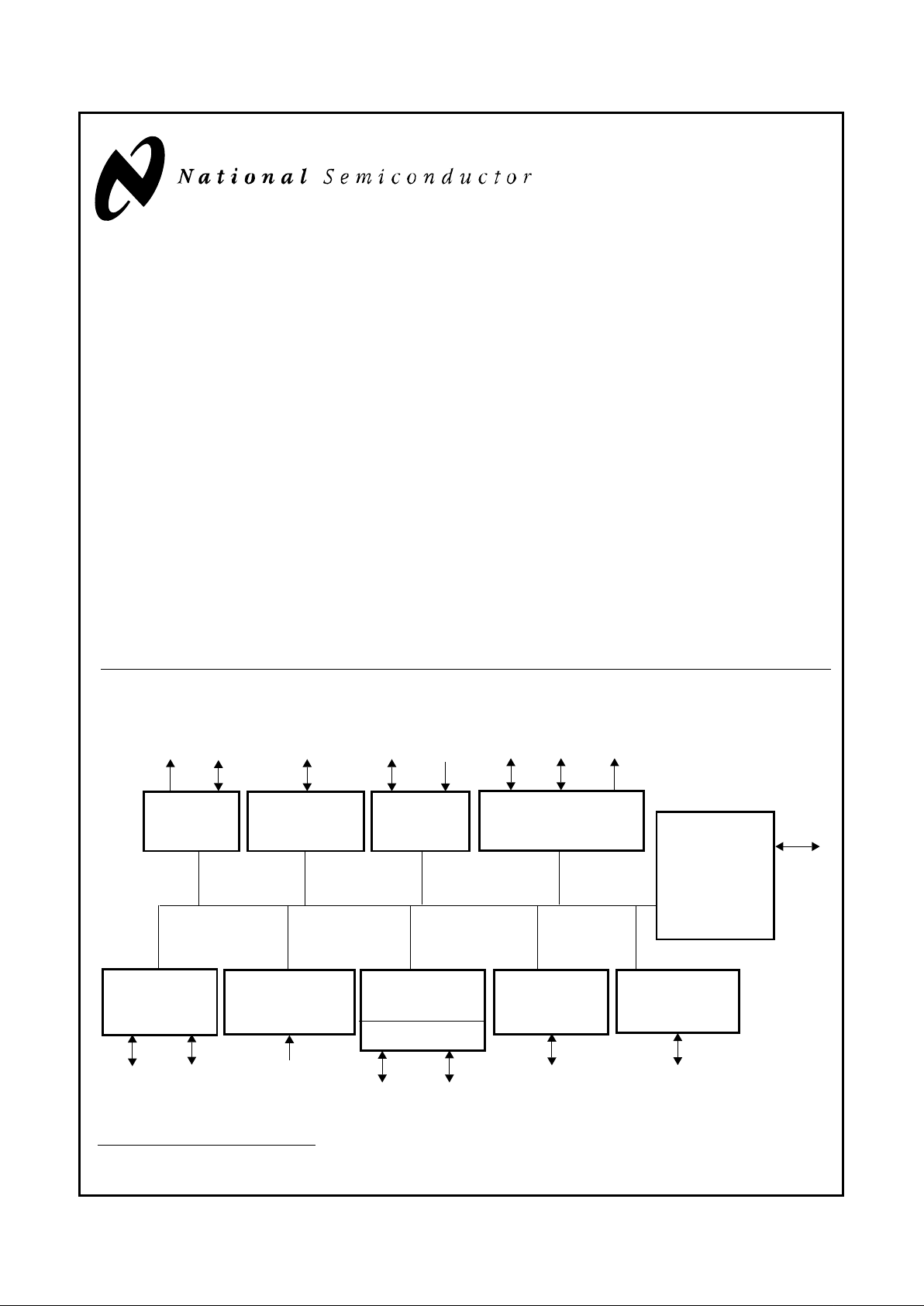
Block Diagram
Real-Time Clock
(Logical Device 2)
Floppy Disk
Controller (FDC)
with Digital Data
Separator (DDS)
(PC8477)
High Current Driver
Keyboard
Controller (KBC)
Power Management
Logic
µP Address
Floppy
Drive
Interface
Data Handshake
Data
Serial
Two UARTs + IR
(16550 or 16450)
X-Bus
IEEE1284
Control
Parallel Port
Interface
Infrared
Interface
Ports
(PnP)
IRQ
Control
DMA
Channels
(Logical Devices 5 & 6)
Interrupt
(RTC and APC)
Plug and Play
(Logical Device 8)
(Logical Device 0)
Data and
Control
(Logical Device 3)
Data and
Mouse
Controller
(Logical Device 1)
General Purpose
I/O Registers
(Logical Device 7)
I/O Ports
Data and
Control
(Logical Device 4)
Control
Control
© 1998 National Semiconductor Corporation
TRI-STATE® is a registered trademark of National Semiconductor Corporation.
IBM
®
, MicroChannel®, PC-AT® and PS/2® are registered trademarks of International Business Machines Corporation.
Microsoft
®
and Windows® are registered trademarks of Microsoft Corporation.
Page 2

2
Highlights
www.national.com
■ A special Plug and Play (PnP) module that includes:
— Flexible IRQs, DMAs and base addresses that meet
the Plug and Play requirements specified by Microsoft
®
in their 1995 hardware design guide for
Windows
®
and Plug and Play ISA Revision 1.0A
— Plug and Play ISA mode (with isolation mechanism
– Wait for Key state)
— Motherboard Plug and Play mode
■ A Floppy Disk Controller (FDC) that provides:
— A modifiable address that is referenced by a 16-bit
programmable register
— Software compatibility with the PC8477, which con-
tains a superset of the floppy disk controller functions in the µDP8473, the NEC µPD765A and the
N82077
— 13 IRQ channel options
— Four 8-bit DMA channel options
— 16-byte FIFO
— Burst and non-burst modes
— A high-performance, internal, digital data separator
that does not require any external filter components
— Support for standard 5.25" and 3.5" floppy disk
drives
— Automatic media sense support
— Perpendicular recording drive support
— Three-mode Floppy Disk Drive (FDD) support
— Full support for the IBM Tape Drive Register (TDR)
implementation of AT and PS/2 drive types
■ A Keyboard and mouse Controller (KBC) with:
— A modifiable address that is referenced by a 16-bit
programmable register, reported as a fixed address
in resource data
— 13 IRQ options for the keyboard controller
— 13 IRQ options for the mouse controller
— An 8-bit microcontroller
— Software compatibility with the 8042AH and
PC87911 microcontrollers
— 2 KB of custom-designed program ROM
— 256 bytes of RAM for data
— Five programmable dedicated open drain I/O lines
for keyboard controller applications
— Asynchronous access to two data registers and one
status register during normal operation
— Support for both interrupt and polling
— 93 instructions
— An 8-bit timer/counter
— Support for binary and BCD arithmetic
— Operation at 8 MHz,12 MHz or 16 MHz (programma-
ble option)
— Can be customized using the PC87323VUL, which
includes a RAM-based KBC, as a development platform for keyboard controller code
■ A Real-Time Clock (RTC) that has:
— A modifiable address that is referenced by a 16-bit
programmable register
— 13 IRQ options, with programmable polarity
— DS1287, MC146818 and PC87911 compatibility
— 242 bytes of battery backed up CMOS RAM in two
banks
— Selective lock mechanism for the RTC RAM
— Battery backed up century calendar in days, days of
the week, months and years, with automatic leapyear adjustment
— Battery backed-up time of day in seconds, minutes
and hours that allows a 12 or 24 hour format and adjustments for daylight savings time
— BCD or binary format for time keeping
— Three different maskable interrupt flags:
• Periodic interrupts - At intervals from 122 msec
to 500 msec
• Time-of-day alarm - At intervals from once per
second to once per day
• Updated Ended Interrupt - Once per second
upon completion of update
— Separate battery pin, 2.4 V operation that includes
an internal UL protection resistor
— 2 µA maximum power consumption during power
down
— Double-buffer time registers
■ An Advanced Power supply Control (APC) that controls
the main power supply to the system, using open-drain
output, as follows:
Power turned on when:
— The RTC reaches a pre-determined date and time.
— A high to low transition occurs on the
RI input signals
of the UARTs.
— A ring pulse or pulse train is detected on the
RING
input signal.
— A SWITCH input signal indicates a Switch On event
Powered turned off when:
— A SWITCH input signal indicates a Switch Off event
— A Fail-safe event occurs (power-save mode detect-
ed but the system is hung up).
— Software turns power off.
■ Two UARTs that provide:
— Software compatibility with the 16550A and the
16450
— A modifiable address that is referenced by a 16-bit
programmable register
— 13 IRQ channel options
— Shadow register support for write-only bits
— Four 8-bit DMA options for the UART with Infrared
support (UART2)
■ An enhanced UART and Infrared (IR) interface on the
UART2 that supports:
— UART data rates up to 1.5 Mbaud
— IrDA 1.0 SIR
— ASK-IR option of SHARP-IR
— DASK-IR option of SHARP-IR
— Consumer-IR (TV-Remote) circuitry
— A Plug and Play compatible external transceiver
■ A bidirectional parallel port that includes:
— A modifiable address that is referenced by a 16-bit
programmable register
Page 3

3
Highlights
www.national.com
— Software or hardware control
— 13 IRQ channel options
— Four 8-bit DMA channel options
— Demand mode DMA support
— An Enhanced Parallel Port (EPP) that is compatible
with the new version EPP 1.9, and is IEEE1284
compliant
— An Enhanced Parallel Port (EPP) that also supports
version EPP 1.7 of the Xircom specification.
— Support for an Enhanced Parallel Port (EPP) as
mode 4 of the Extended Capabilities Port (ECP)
— An Extended Capabilities Port (ECP) that is IEEE
1284 compliant, including level 2
— Selection of internal pull-up or pull-down resistor for
Paper End (PE) pin
— Reduction of PCI bus utilization by supporting a de-
mand DMA mode mechanism and a DMA fairness
mechanism
— A protection circuit that prevents damage to the par-
allel port when a printer connected to it powers up or
is operated at high voltages
— Output buffers that can sink and source14 mA
■ Three general purpose pins for three separate programmable chip select signals, as follows:
— Can be programmed for game port control
— The Chip Select 0 (
CS0) signal produces open drain
output and is powered by the V
CCH
— The Chip Select 1 (CS1) and 2 (CS2) signals have
push-pull buffers and are powered by the main V
DD
— Decoding of chip select signals depends on the ad-
dress and the Address Enable (AEN) signals, and
can be qualified using the Read (
RD) and Write
(
WR) signals.
■ 16 single-bit General Purpose I/O ports (GPIO):
— Modifiable addresses that are referenced by a 16-bit
programmable register
— Programmable direction for each signal (input or
output) with configuration lock
— Programmable drive type for each output pin (open-
drain or push-pull) with configuration lock
— Programmable option for internal pull-up resistor on
each input pin with configuration lock
— A back-drive protection circuit
■ An X-bus data buffer that connects the 8-bit X data bus
to the ISA data bus
■ Clock source options:
— Source is a 32.768 KHz crystal - an internal frequen-
cy multiplier generates all the required internal frequencies.
— Source may be either a 48 MHz or 24 MHz clock in-
put signal.
■ Enhanced Power Management (PM), including:
— Special configuration registers for power down
— WATCHDOG timer for power-saving strategies
— Reduced current leakage from pins
— Low-power CMOS technology
— Ability to shut off clocks to all modules
■ General features include:
— All accesses to the SuperI/O chip activate a Zero
Wait State (
ZWS) signal, except for accesses to the
Enhanced Parallel Port (EPP) and to configuration
registers
— Access to all configuration registers is through an In-
dex and a Data register, which can be relocated
within the ISA I/O address space
— 160-pin Plastic Quad Flatpack (PQFP) package
Page 4
4
Highlights
www.national.com
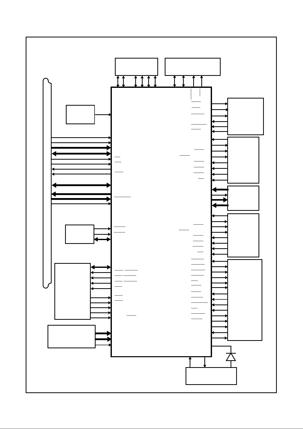
DRATE0
Parallel
Port
Connector
Configuration
Select Logic
Clock
Power
Management
EIA
Drivers
EIA
Drivers
FDC
Connector
ONCTL
ISA Bus
Basic Configuration
X1
MR
AEN
A15-0
D7-0
RD
WR
TC
PD7-0
SLIN/ASTRB
STB/WRITE
AFD/DSTRB
INIT
ACK
ERR
SLCT
PE
BUSY/WAIT
BADDR1,0
CFG3-0
V
CCH
SWITCH
RING
SIN1
SOUT1
RTS1
DTR1/BOUT1
CTS1
DSR1
DCD1
RI1
SIN2
SOUT2
RTS2
DTR2/BOUT2
CTS2
DSR2
DCD2
RI2
RDATA
WDATA
WGATE
HDSEL
DIR
STEP
TRK0
INDEX
DSKCHG
WP
MTR1,0
DR1,0
DENSEL
IOCHRDY
ZWS
RTC Crystal
and Power
V
BAT
X1C X2C
DRQ3-0
DACK3-0
P17,16,12
P21,20
KBCLK
KBDAT
MDAT
MCLK
CS2
Keyboard I/O
Interface
General
Purpose Registers
CS1,0
MSEN1,0
GPIO27-20
GPIO17-10
IRQ1
Infrared
Interface
IRRX2,1
IRTX
PC87307/PC97307
IRQ12-3
IRQ15-14
IRSL2-0
SELCS
X-Bus
XDCS
XD7-0
XDRD
WDO
POR
ID3-0
Page 5

5
Table of Contents
www.national.com
Table of Contents
Highlights.............................................................................................................................1
1.0
Signal/Pin Connection and Description
1.1 CONNECTION DIAGRAM .........................................................................................................14
1.2 SIGNAL/PIN DESCRIPTIONS ...................................................................................................15
2.0
Configuration
2.1 HARDWARE CONFIGURATION ...............................................................................................24
2.1.1 Wake Up Options ........................................................................................................24
2.1.2 The Index and Data Register Pair ...............................................................................24
2.1.3 The Strap Pins .............................................................................................................25
2.2 SOFTWARE CONFIGURATION ...............................................................................................25
2.2.1 Accessing the Configuration Registers ........................................................................25
2.2.2 Address Decoding .......................................................................................................25
2.3 THE CONFIGURATION REGISTERS .......................................................................................26
2.3.1 Standard Plug and Play (PnP) Register Definitions ....................................................27
2.3.2 Configuration Register Summary ................................................................................30
2.4 CARD CONTROL REGISTERS ................................................................................................34
2.4.1 SID Register (In PC87307) ..........................................................................................34
2.4.2 SID Register (In PC97307) ..........................................................................................34
2.4.3 SuperI/O Configuration 1 Register, Index 21h .............................................................34
2.4.4 SuperI/O Configuration 2 Register, Index 22h .............................................................35
2.4.5 Programmable Chip Select Configuration Index Register, Index 23h .........................35
2.4.6 Programmable Chip Select Configuration Data Register, Index 24h ..........................36
2.4.7 SRID Register (In PC97307 only) ................................................................................36
2.5 KBC CONFIGURATION REGISTER (LOGICAL DEVICE 0) ....................................................36
2.5.1 SuperI/O KBC Configuration Register, Index F0h .......................................................36
2.6 FDC CONFIGURATION REGISTERS (LOGICAL DEVICE 3) ..................................................36
2.6.1 SuperI/O FDC Configuration Register, Index F0h .......................................................36
2.6.2 Drive ID Register, Index F1h .......................................................................................37
2.7 PARALLEL PORT CONFIGURATION REGISTER (LOGICAL DEVICE 4) ...............................37
2.7.1 SuperI/O Parallel Port Configuration Register, Index F0h ...........................................37
2.8 UART2 AND INFRARED CONFIGURATION REGISTER (LOGICAL DEVICE 5) ....................38
2.8.1 SuperI/O UART2 Configuration Register, Index F0h ...................................................38
2.9 UART1 CONFIGURATION REGISTER (LOGICAL DEVICE 6) ................................................38
2.9.1 SuperI/O UART1 Configuration Register, Index F0h ...................................................38
2.10 PROGRAMMABLE CHIP SELECT CONFIGURATION REGISTERS ......................................39
2.10.1 CS0 Base Address MSB, Second Level Index 00h .....................................................39
2.10.2 CS0 Base Address LSB Register, Second Level Index 01h .......................................39
2.10.3 CS0 Configuration Register, Second Level Index 02h ................................................39
2.10.4 Reserved, Second Level Index 03h .............................................................................39
2.10.5 CS1 Base Address MSB Register, Second Level Index 04h ......................................40
2.10.6 CS1 Base Address LSB Register, Second Level Index 05h .......................................40
Page 6

6
Table of Contents
www.national.com
2.10.7 CS1 Configuration Register, Second Level Index 06h ................................................40
2.10.8 Reserved, Second Level Index 07h .............................................................................40
2.10.9 CS2 Base Address MSB Register, Second Level Index 08h ......................................40
2.10.10 CS2 Base Address LSB Register, Second Level Index 09h .......................................40
2.10.11 CS2 Configuration Register, Second Level Index 0Ah ................................................40
2.10.12 Reserved, Second Level Indexes 0Bh-0Fh .................................................................40
2.10.13 Not Accessible, Second Level Indexes 10h-FFh .........................................................40
2.11 CARD CONTROL REGISTER BITMAPS ..................................................................................41
3.0
Keyboard (and Mouse) Controller (KBC) (Logical Devices 0 and 1)
3.1 SYSTEM ARCHITECTURE .......................................................................................................43
3.2 FUNCTIONAL OVERVIEW .......................................................................................................44
3.3 DEVICE CONFIGURATION ......................................................................................................44
3.3.1 I/O Address Space ......................................................................................................44
3.3.2 Interrupt Request Signals ............................................................................................44
3.3.3 KBC Clock ...................................................................................................................45
3.3.4 Timer or Event Counter ...............................................................................................46
3.4 EXTERNAL I/O INTERFACES ..................................................................................................46
3.4.1 Keyboard and Mouse Interface ...................................................................................46
3.4.2 General Purpose I/O Signals .......................................................................................46
3.5 INTERNAL KBC - PC87307/PC97307 INTERFACE .................................................................47
3.5.1 The KBC DBBOUT Register, Offset 60h, Read Only ..................................................47
3.5.2 The KBC DBBIN Register, Offset 60h (F1 Clear) or 64h (F1 Set), Write Only ............47
3.5.3 The KBC STATUS Register, Offset 64h, Read Only ...................................................48
3.6 INSTRUCTION TIMING .............................................................................................................48
4.0
Real-Time Clock (RTC) and Advanced Power Control (APC) (Logical Device 2)
4.1 RTC OPERATION OVERVIEW .................................................................................................49
4.1.1 RTC Hardware and Functional Description .................................................................49
4.1.2 Timekeeping ................................................................................................................50
4.1.3 Power Supply ..............................................................................................................51
4.1.4 Interrupt Handling ........................................................................................................52
4.2 THE RTC REGISTERS .............................................................................................................52
4.2.1 RTC Control Register A (CRA), Index 0Ah ..................................................................52
4.2.2 RTC Control Register B (CRB), Index 0Bh .................................................................54
4.2.3 RTC Control Register C (CRC), Index 0Ch .................................................................54
4.2.4 RTC Control Register D (CRD), Index 0Dh .................................................................55
4.3 APC OVERVIEW .......................................................................................................................55
4.3.1 User Selectable Parameters ........................................................................................55
4.3.2 System Power States ..................................................................................................56
4.3.3 System Power Switching Logic ...................................................................................56
4.4 DETAILED FUNCTIONAL DESCRIPTION ................................................................................58
4.4.1 The ONCTL Signal ......................................................................................................58
4.4.2 Entering Power States .................................................................................................58
4.4.3 System Power-Up and Power-Off Activation Event Description ..................................59
Page 7

7
Table of Contents
www.national.com
4.5 APC REGISTERS ......................................................................................................................60
4.5.1 APC Control Register 1 (APCR1), Index 40h ..............................................................60
4.5.2 APC Control Register 2 (APCR2), Index 41h ..............................................................61
4.5.3 APC Status Register (APSR), Index 42h .....................................................................61
4.5.4 RAM Lock Register (RLR), Index 47h .........................................................................62
4.6 RTC AND APC REGISTER BITMAPS ......................................................................................62
4.6.1 RTC Register Bitmaps .................................................................................................62
4.6.2 APC Register Bitmaps .................................................................................................63
4.7 REGISTER BANK TABLES .......................................................................................................64
5.0
The Digital Floppy Disk Controller (FDC) (Logical Device 3)
5.1 FDC FUNCTIONS .....................................................................................................................66
5.1.1 Microprocessor Interface .............................................................................................66
5.1.2 System Operation Modes ............................................................................................66
5.2 DATA TRANSFER .....................................................................................................................67
5.2.1 Data Rates ...................................................................................................................67
5.2.2 The Data Separator .....................................................................................................67
5.2.3 Perpendicular Recording Mode Support .....................................................................68
5.2.4 Data Rate Selection .....................................................................................................68
5.2.5 Write Precompensation ...............................................................................................69
5.2.6 FDC Low-Power Mode Logic .......................................................................................69
5.2.7 Reset ...........................................................................................................................69
5.3 THE REGISTERS OF THE FDC ...............................................................................................70
5.3.1 Status Register A (SRA), Offset 00h ...........................................................................70
5.3.2 Status Register B (SRB), Offset 01h ...........................................................................71
5.3.3 Digital Output Register (DOR), Offset 02h ..................................................................71
5.3.4 Tape Drive Register (TDR), Offset 03h .......................................................................73
5.3.5 Main Status Register (MSR), Offset 04h, Read Operations ........................................74
5.3.6 Data Rate Select Register (DSR), Offset 04h, Write Operations ................................75
5.3.7 Data Register (FIFO), Offset 05h ................................................................................76
5.3.8 Digital Input Register (DIR), Offset 07h, Read Operations ..........................................77
5.3.9 Configuration Control Register (CCR), Offset 07h, Write Operations .........................78
5.4 THE PHASES OF FDC COMMANDS .......................................................................................78
5.4.1 Command Phase .........................................................................................................78
5.4.2 Execution Phase ..........................................................................................................78
5.4.3 Result Phase ...............................................................................................................80
5.4.4 Idle Phase ....................................................................................................................80
5.4.5 Drive Polling Phase .....................................................................................................80
5.5 THE RESULT PHASE STATUS REGISTERS ..........................................................................81
5.5.1 Result Phase Status Register 0 (ST0) .........................................................................81
5.5.2 Result Phase Status Register 1 (ST1) .........................................................................81
5.5.3 Result Phase Status Register 2 (ST2) .........................................................................82
5.5.4 Result Phase Status Register 3 (ST3) .........................................................................83
5.6 FDC REGISTER BITMAPS .......................................................................................................84
5.6.1 FDC Standard Register Bitmaps .................................................................................84
Page 8

8
Table of Contents
www.national.com
5.6.2 FDC Result Phase Status Register Bitmaps ...............................................................85
5.7 THE FDC COMMAND SET .......................................................................................................86
5.7.1 Abbreviations Used in FDC Commands ......................................................................87
5.7.2 The CONFIGURE Command ......................................................................................88
5.7.3 The DUMPREG Command .........................................................................................88
5.7.4 The FORMAT TRACK Command ...............................................................................89
5.7.5 The INVALID Command ..............................................................................................92
5.7.6 The LOCK Command ..................................................................................................92
5.7.7 The MODE Command .................................................................................................92
5.7.8 The NSC Command ....................................................................................................94
5.7.9 The PERPENDICULAR MODE Command .................................................................94
5.7.10 The READ DATA Command .......................................................................................96
5.7.11 The READ DELETED DATA Command ......................................................................98
5.7.12 The READ ID Command .............................................................................................99
5.7.13 The READ A TRACK Command ...............................................................................100
5.7.14 The RECALIBRATE Command .................................................................................100
5.7.15 The RELATIVE SEEK Command ..............................................................................101
5.7.16 The SCAN EQUAL, the SCAN LOW OR EQUAL and the SCAN HIGH OR EQUAL
Commands ..........................................................................................................101
5.7.17 The SEEK Command ................................................................................................102
5.7.18 The SENSE DRIVE STATUS Command ..................................................................103
5.7.19 The SENSE INTERRUPT Command ........................................................................103
5.7.20 The SET TRACK Command ......................................................................................104
5.7.21 The SPECIFY Command ..........................................................................................105
5.7.22 The VERIFY Command .............................................................................................106
5.7.23 The VERSION Command ..........................................................................................108
5.7.24 The WRITE DATA Command ....................................................................................108
5.7.25 The WRITE DELETED DATA Command ..................................................................109
5.8 EXAMPLE OF A FOUR-DRIVE CIRCUIT USING THE PC87307/PC97307 ...........................110
6.0
Parallel Port (Logical Device 4)
6.1 PARALLEL PORT CONFIGURATION ....................................................................................111
6.1.1 Parallel Port Operation Modes ..................................................................................111
6.1.2 Configuring Operation Modes ....................................................................................111
6.1.3 Output Pin Protection ................................................................................................111
6.2 STANDARD PARALLEL PORT (SPP) MODES ......................................................................111
6.2.1 Standard Parallel Port (SPP) Modes Register Set ....................................................112
6.2.2 SPP Data Register (DTR), Offset 00h .......................................................................112
6.2.3 Status Register (STR), Offset 01h .............................................................................113
6.2.4 SPP Control Register (CTR), Offset 02h ...................................................................114
6.3 ENHANCED PARALLEL PORT (EPP) MODES ......................................................................115
6.3.1 Enhanced Parallel Port (EPP) Register Set ..............................................................115
6.3.2 SPP or EPP Data Register (DTR), Offset 00h ...........................................................115
6.3.3 SPP or EPP Status Register (STR), Offset 01h ........................................................115
6.3.4 SPP or EPP Control Register (CTR), Offset 02h .......................................................116
6.3.5 EPP Address Register (ADDR), Offset 03h ...............................................................116
6.3.6 EPP Data Register 0 (DATA0), Offset 04h ................................................................116
Page 9

9
Table of Contents
www.national.com
6.3.7 EPP Data Register 1 (DATA1), Offset 05h ................................................................116
6.3.8 EPP Data Register 2 (DATA2), Offset 06h ................................................................116
6.3.9 EPP Data Register 3 (DATA3), Offset 07h ................................................................117
6.3.10 EPP Mode Transfer Operations ................................................................................117
6.3.11 EPP 1.7 and 1.9 Zero Wait State Data Write and Read Operations .........................118
6.4 EXTENDED CAPABILITIES PARALLEL PORT (ECP) ...........................................................119
6.4.1 ECP Modes ...............................................................................................................119
6.4.2 Software Operation ....................................................................................................119
6.4.3 Hardware Operation ..................................................................................................119
6.5 ECP MODE REGISTERS ........................................................................................................120
6.5.1 Accessing the ECP Registers ....................................................................................120
6.5.2 Second Level Offsets ................................................................................................120
6.5.3 ECP Data Register (DATAR), Bits 7-5 of ECR = 000 or 001, Offset 000h ................121
6.5.4 ECP Address FIFO (AFIFO) Register, Bits 7-5 of ECR = 011, Offset 000h ..............121
6.5.5 ECP Status Register (DSR), Offset 001h ..................................................................121
6.5.6 ECP Control Register (DCR), Offset 002h ................................................................122
6.5.7 Parallel Port Data FIFO (CFIFO) Register, Bits 7-5 of ECR = 010, Offset 400h .......122
6.5.8 ECP Data FIFO (DFIFO) Register, Bits 7-5 of ECR = 011, Offset 400h ...................122
6.5.9 Test FIFO (TFIFO) Register, Bits 7-5 of ECR = 110, Offset 400h .............................123
6.5.10 Configuration Register A (CNFGA), Bits 7-5 of ECR = 111, Offset 400h ..................123
6.5.11 Configuration Register B (CNFGB), Bits 7-5 of ECR = 111, Offset 401h ..................123
6.5.12 Extended Control Register (ECR), Offset 402h .........................................................124
6.5.13 ECP Extended Index Register (EIR), Offset 403h .....................................................125
6.5.14 ECP Extended Data Register (EDR), Offset 404h ....................................................126
6.5.15 ECP Extended Auxiliary Status Register (EAR), Offset 405h ...................................126
6.5.16 Control0, Second Level Offset 00h ............................................................................126
6.5.17 Control2, Second Level Offset 02h ............................................................................126
6.5.18 Control4, Second Level Offset 04h ............................................................................127
6.5.19 PP Confg0, Second Level Offset 05h ........................................................................127
6.6 DETAILED ECP MODE DESCRIPTIONS ...............................................................................128
6.6.1 Software Controlled Data Transfer (Modes 000 and 001) .........................................128
6.6.2 Automatic Data Transfer (Modes 010 and 011) ........................................................128
6.6.3 Automatic Address and Data Transfers (Mode 100) .................................................130
6.6.4 FIFO Test Access (Mode 110) ..................................................................................130
6.6.5 Configuration Registers Access (Mode 111) .............................................................130
6.6.6 Interrupt Generation ..................................................................................................130
6.7 PARALLEL PORT REGISTER BITMAPS ...............................................................................131
6.7.1 EPP Modes Parallel Port Register Bitmaps ...............................................................131
6.7.2 ECP Modes Parallel Port Register Bitmaps ..............................................................132
6.8 PARALLEL PORT PIN/SIGNAL LIST ......................................................................................134
7.0
UART1 and UART2 (with IR) (Logical Devices 5 and 6)
7.1 FEATURES ..............................................................................................................................135
7.2 FUNCTIONAL MODES OVERVIEW .......................................................................................135
7.2.1 UART Modes: 16450 or 16550, and Extended ..........................................................135
7.2.2 Sharp-IR, IrDA SIR Infrared Modes ...........................................................................135
Page 10

10
Table of Contents
www.national.com
7.2.3 Consumer IR Mode ...................................................................................................135
7.3 REGISTER BANK OVERVIEW ...............................................................................................136
7.4 UART MODES – DETAILED DESCRIPTION ..........................................................................136
7.4.1 16450 or 16550 UART Mode .....................................................................................137
7.4.2 Extended UART Mode ...............................................................................................137
7.5 SHARP-IR MODE – DETAILED DESCRIPTION .....................................................................138
7.6 SIR MODE – DETAILED DESCRIPTION ................................................................................138
7.7 CONSUMER-IR MODE – DETAILED DESCRIPTION ............................................................138
7.7.1 Consumer-IR Transmission .......................................................................................138
7.7.2 Consumer-IR Reception ............................................................................................138
7.8 FIFO TIME-OUTS ....................................................................................................................139
7.8.1 UART, SIR or Sharp-IR Mode Time-Out Conditions .................................................139
7.8.2 Consumer-IR Mode Time-Out Conditions .................................................................139
7.8.3 Transmission Deferral ...............................................................................................139
7.9 AUTOMATIC FALLBACK TO A NON-EXTENDED UART MODE ..........................................140
7.10 OPTICAL TRANSCEIVER INTERFACE .................................................................................140
7.11 BANK 0 – GLOBAL CONTROL AND STATUS REGISTERS .................................................140
7.11.1 Receiver Data Port (RXD) or the Transmitter Data Port (TXD), Bank 0, Offset 00h .141
7.11.2 Interrupt Enable Register (IER), Bank 0, Offset 01h .................................................141
7.11.3 Event Identification Register (EIR), Bank 0, Offset 02h .............................................143
7.11.4 FIFO Control Register (FCR), Bank 0, Offset 02h .....................................................145
7.11.5 Link Control Register (LCR), Bank 0, Offset 03h, and Bank Selection Register (BSR),
All Banks, Offset 03h ...........................................................................................145
7.11.6 Bank Selection Register (BSR), All Banks, Offset 03h ..............................................147
7.11.7 Modem/Mode Control Register (MCR), Bank 0, Offset 04h ......................................147
7.11.8 Link Status Register (LSR), Bank 0, Offset 05h ........................................................148
7.11.9 Modem Status Register (MSR), Bank 0, Offset 06h ..................................................149
7.11.10 Scratchpad Register (SPR), Bank 0, Offset 07h .......................................................150
7.11.11 Auxiliary Status and Control Register (ASCR), Bank 0, Offset 07h ...........................150
7.11.12 Legacy Baud Generator Divisor Ports (LBGD(L) and LBGD(H)),
Bank 1, Offsets 00h and 01h ...............................................................................151
7.11.13 Link Control Register (LCR) and Bank Select Register (BSR), Bank 1, Offset 03h ..152
7.12 BANK 2 – EXTENDED CONTROL AND STATUS REGISTERS ............................................152
7.12.1 Baud Generator Divisor Ports, LSB (BGD(L)) and
MSB (BGD(H)),Bank 2, Offsets 00h and 01h ......................................................152
7.12.2 Extended Control Register 1 (EXCR1), Bank 2, Offset 02h ......................................154
7.12.3 Link Control Register (LCR) and Bank Select Register (BSR), Bank 2, Offset 03h ..155
7.12.4 Extended Control and Status Register 2 (EXCR2), Bank 2, Offset 04h ....................155
7.12.5 Reserved Register, Bank 2, Offset 05h .....................................................................155
7.12.6 TX_FIFO Current Level Register (TXFLV), Bank 2, Offset 06h ................................155
7.12.7 RX_FIFO Current Level Register (RXFLV), IrDA or Consumer-IR Modes,
Bank 2, Offset 07h ..............................................................................................156
7.13 BANK 3 – MODULE REVISION ID AND SHADOW REGISTERS ..........................................156
7.13.1 Module Revision ID Register (MRID), Bank 3, Offset 00h .........................................156
7.13.2 Shadow of Link Control Register (SH_LCR), Bank 3, Offset 01h ..............................157
Page 11

11
Table of Contents
www.national.com
7.13.3 Shadow of FIFO Control Register (SH_FCR), Bank 3, Offset 02h ............................157
7.13.4 Link Control Register (LCR) and Bank Select Register (BSR), Bank 3, Offset 03h ..157
7.14 BANK 4 – IR MODE SETUP REGISTER ................................................................................157
7.14.1 Reserved Registers, Bank 4, Offsets 00h and 01h ...................................................157
7.14.2 Infrared Control Register 1 (IRCR1), Bank 4, Offset 02h ..........................................157
7.14.3 Link Control Register (LCR) and Bank Select Register (BSR), Bank 4, Offset 03h ..158
7.14.4 Reserved Registers, Bank 4, Offsets 04h -07h .........................................................158
7.15 BANK 5 – INFRARED CONTROL REGISTERS .....................................................................158
7.15.1 Reserved Registers, Bank 5, Offsets 00h -02h .........................................................158
7.15.2 (LCR/BSR) Register, Bank 5, Offset 03h ..................................................................158
7.15.3 Infrared Control Register 2 (IRCR2), Bank 5, Offset 04h ..........................................158
7.15.4 Reserved Registers, Bank 5, Offsets 05h -07h .........................................................158
7.16 BANK 6 – INFRARED PHYSICAL LAYER CONFIGURATION REGISTERS .........................159
7.16.1 Infrared Control Register 3 (IRCR3), Bank 6, Offset 00h ..........................................159
7.16.2 Reserved Register, Bank 6, Offset 01h .....................................................................159
7.16.3 SIR Pulse Width Register (SIR_PW), Bank 6, Offset 02h .........................................159
7.16.4 Link Control Register (LCR) and Bank Select Register (BSR), Bank 6, Offset 03h ..159
7.16.5 Reserved Registers, Bank 6, Offsets 04h-07h ..........................................................159
7.17 BANK 7 – CONSUMER-IR AND OPTICAL TRANSCEIVER CONFIGURATION REGISTERS 159
7.17.1 Infrared Receiver Demodulator Control Register (IRRXDC), Bank 7, Offset 0 .........160
7.17.2 Infrared Transmitter Modulator Control Register (IRTXMC), Bank 7, Offset 01h ......160
7.17.3 Consumer-IR Configuration Register (RCCFG), Bank 7, Offset 02h ........................163
7.17.4 Link Control/Bank Select Registers (LCR/BSR), Bank 7, Offset 03h ........................163
7.17.5 Infrared Interface Configuration Register 1 (IRCFG1), Bank 7, Offset 04h ...............163
7.17.6 Reserved Register, Bank 7, Offset 05h .....................................................................164
7.17.7 Infrared Interface Configuration 3 Register (IRCFG3), Bank 7, Offset 06h ...............164
7.17.8 Infrared Interface Configuration Register 4 (IRCFG4), Bank 7, Offset 07h ...............164
7.18 UART2 REGISTER WITH FAST IR REGISTER BITMAPS ....................................................165
8.0
General Purpose Input and Output (GPIO) Ports (Logical Device 7) and Chip
Select Output Signals
8.1 GENERAL PURPOSE INPUT AND OUTPUT (GPIO) PORTS ...............................................170
8.2 PROGRAMMABLE CHIP SELECT OUTPUT SIGNALS .........................................................171
9.0
Power Management (Logical Device 8)
9.1 POWER MANAGEMENT OPTIONS .......................................................................................172
9.1.1 Configuration Options ................................................................................................172
9.1.2 The WATCHDOG Feature .........................................................................................172
9.2 THE POWER MANAGEMENT REGISTERS ..........................................................................172
9.2.1 Power Management Index Register, Base Address + 00h ........................................172
9.2.2 Power Management Data Register, Base Address + 01h .........................................173
9.2.3 Function Enable Register 1 (FER1), Index 00h .........................................................173
9.2.4 Function Enable Register 2 (FER2), Index 01h .........................................................173
9.2.5 Power Management Control 1 Register (PMC1), Index 02h .....................................174
9.2.6 Power Management Control 2 Register (PMC2), Index 03h .....................................174
Page 12

12
Table of Contents
www.national.com
9.2.7 Power Management Control 3 Register (PMC3), Index 04h .....................................175
9.2.8 Watchdog Time-Out (WDTO) Register, Index 05h ....................................................175
9.2.9 WATCHDOG Configuration Register (WDCF), Index 06h ........................................175
9.2.10 WATCHDOG Status Register (WDST), Index 07h ....................................................176
9.3 POWER MANAGEMENT REGISTER BITMAPS ....................................................................177
10.0
X-Bus Data Buffer
10.1 FUNCTIONAL OVERVIEW .....................................................................................................179
10.2 MAPPING ................................................................................................................................179
11.0
The Internal Clock
11.1 THE CLOCK SOURCE ............................................................................................................180
11.2 THE INTERNAL ON-CHIP CLOCK MULTIPLIER ...................................................................180
11.3 SPECIFICATIONS ...................................................................................................................180
12.0
Interrupt and DMA Mapping
12.1 IRQ MAPPING .........................................................................................................................181
12.2 DMA MAPPING .......................................................................................................................181
13.0
Device Description
13.1 GENERAL DC ELECTRICAL CHARACTERISTICS ...............................................................182
13.1.1 Recommended Operating Conditions .......................................................................182
13.1.2 Absolute Maximum Ratings .......................................................................................182
13.1.3 Capacitance ...............................................................................................................182
13.1.4 Power Consumption Under Recommended Operating Conditions ...........................183
13.2 DC CHARACTERISTICS OF PINS, BY GROUP ....................................................................183
13.2.1 Group 1 ......................................................................................................................183
13.2.2 Group 2 ......................................................................................................................184
13.2.3 Group 3 ......................................................................................................................184
13.2.4 Group 4 ......................................................................................................................184
13.2.5 Group 5 ......................................................................................................................185
13.2.6 Group 6 ......................................................................................................................185
13.2.7 Group 7 ......................................................................................................................185
13.2.8 Group 8 ......................................................................................................................186
13.2.9 Group 9 ......................................................................................................................186
13.2.10 Group 10 ....................................................................................................................187
13.2.11 Group 11 ....................................................................................................................187
13.2.12 Group 12 ....................................................................................................................188
13.2.13 Group 13 ....................................................................................................................188
13.2.14 Group 14 ....................................................................................................................189
13.2.15 Group 15 ....................................................................................................................189
13.2.16 Group 16 ....................................................................................................................189
13.2.17 Group 17 ....................................................................................................................190
13.2.18 Group 18 ....................................................................................................................190
13.2.19 Group 19 ....................................................................................................................190
Page 13

13
Table of Contents
www.national.com
13.2.20 Group 20 ....................................................................................................................190
13.2.21 Group 21 ....................................................................................................................190
13.2.22 Group 22 ....................................................................................................................191
13.2.23 Group 23 ....................................................................................................................191
13.3 AC ELECTRICAL CHARACTERISTICS ..................................................................................191
13.3.1 AC Test Conditions TA = 0 °C to 70 °C, VDD = 5.0 V ±10% ......................................191
13.3.2 Clock Timing ..............................................................................................................192
13.3.3 Microprocessor Interface Timing ...............................................................................193
13.3.4 Baud Output Timing ...................................................................................................195
13.3.5 Transmitter Timing .....................................................................................................196
13.3.6 Receiver Timing .........................................................................................................197
13.3.7 UART, Sharp-IR and Consumer-IR Timing ...............................................................199
13.3.8 SIR Timing .................................................................................................................200
13.3.9 IRSLn Write Timing ...................................................................................................200
13.3.10 Modem Control Timing ..............................................................................................201
13.3.11 DMA Timing ...............................................................................................................202
13.3.12 Reset Timing .............................................................................................................204
13.3.13 Write Data Timing ......................................................................................................204
13.3.14 Drive Control Timing ..................................................................................................205
13.3.15 Read Data Timing ......................................................................................................205
13.3.16 Parallel Port Timing ...................................................................................................206
13.3.17 Enhanced Parallel Port 1.7 Timing ............................................................................207
13.3.18 Enhanced Parallel Port 1.9 Timing ............................................................................208
13.3.19 Extended Capabilities Port (ECP) Timing ..................................................................209
13.3.20 GPIO Write Timing ....................................................................................................210
13.3.21 RTC Timing ...............................................................................................................210
13.3.22 APC Timing ...............................................................................................................211
13.3.23 Chip Select Timing ....................................................................................................212
Page 14
14
Signal/Pin Connection and Description
www.national.com
1.0 Signal/Pin Connection and Description
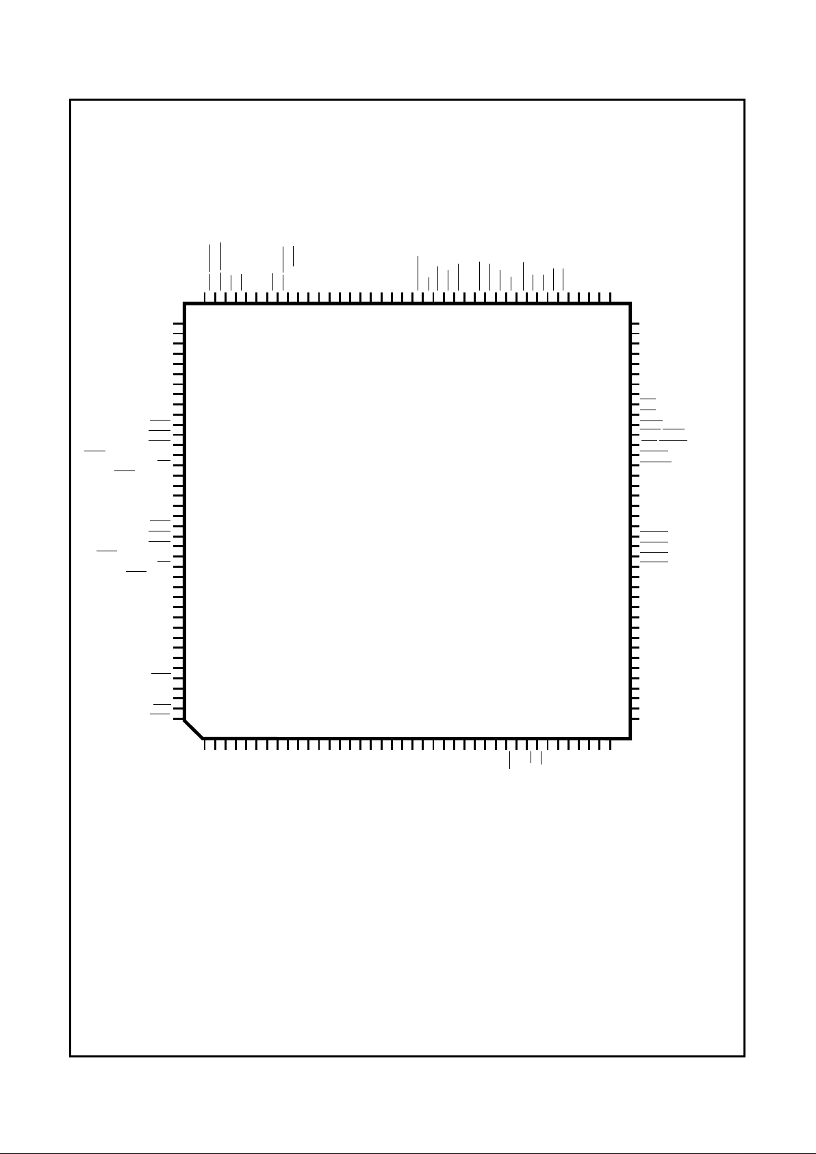
1.1 CONNECTION DIAGRAM
80
75
70
65
60
55
50
1 5 10 15 20 25 30
859095100
4035
PC87307/PC97307
105110115120
45
41
81
121
125
130
135
140
145
150
155
160
A1
A2
V
SS
V
DD
A3A4A5A6A7A8A9
A10
A11
A12
A13
IOCHRDY
RD
ZWS
WGATE
TRK0WPRDATA
HDSEL
A0
MTR1
DSKCHG
DIR
STEP
WDATA
MSEN1
DENSEL
INDEX
MTR0
DR1
DR0
XDRD/ID3
MSEN0
V
DD
P21
P20
P17
P16
P12
GPIO10
GPIO11
GPIO12
GPIO13
CS2/XD1
STB/WRITE
V
SS
V
DD
SLIN/ASTRB
SLCTPEBUSY/
WAIT
ACK
V
DD
INIT
D7
CS1/XD0
X1
V
SS
D0D1D2D3D4D5D6
MR
X2C
V
CCH
A15
A14
V
BAT
X1C
VSSVDDKBCLK
KBDAT
MDAT
MCLK
IRQ15
IRQ14
IRQ12
IRQ11
DACK3
DRATE0
DTR1/BADDR0/BOUT1
RI1
DCD1
DSR1
SIN1
RTS1/BADDR1
SOUT1/CFG0
CTS1
IRQ10
AEN
WR
TC
IRQ9
IRQ8
IRQ7
IRQ6
IRQ1
IRQ3
IRQ4
IRQ5
GPIO14
GPIO15
GPIO16
GPIO17/WDO
GPIO20/IRSL1/ID1
GPIO21/IRSL2/IRSL0/ID2
GPIO22/POR
V
SS
V
DD
DRQ1
DRQ0
DACK2
DACK1
DACK0
DRQ2
DRQ3
ERR
V
SS
V
SS
V
SS
DTR2/CFG1/BOUT2
RI2
DCD2
DSR2
SIN2
RTS2/CFG2
SOUT2/CFG3
CTS2
AFD/DSTRB
PD0
PD1
PD2
PD3
PD4
PD5
PD6
PD7
V
SS
IRTX
IRRX1
IRRX2/IRSL0/ID0
IRSL1/XD7/ID1
IRSL2/XD6/SELCS/GPIO21
GPIO27/XD5
GPIO26/XD4
GPIO25/XD3
GPIO24/XD2
CS0/CSOUT-NSC-Test
ONCTL
SWITCH
RING/XDCS
GPIO23/
RING
Order Number PC87307VUL/PC97307VUL
See NS Package Number VUL160A
PlasticQuad Flatpack (PQFP), EIAJ
Page 15

15
Signal/Pin Connection and Description
www.national.com
1.2 SIGNAL/PIN DESCRIPTIONS
Table 1-1 lists the signals of the part in alphabetical order and shows the pin(s) associated with each. Table 1-2 on page 23
lists the X-Bus Data Buffer (XDB) signals that are multiplexed and Table 1-3 on page 23 lists the pins that have strap functions during reset.
The Module column indicates the functional module that is associated with these pins. In this column, the System label indicates internal functions that are common to more than one module.
The I/O and Group # column describes whether the pin is an input, output, or bidirectional pin (marked as Input, Output or
I/O, respectively). This column also specifies the DC characteristics group to which this pin belongs. See Section 13.2 on
page 183 for details.
Refer to the glossary for an explanation of abbreviations and terms used in this table, and throughout this document. Use
the Table of Contents to find more information about each register.
TABLE 1-1. Signal/Pin Description Table
Signal/Pin
Name
Pin
Number
Module
I/O and
Group #
Function
A15-0 29-26,
23-12
ISA-Bus Input
Group 1
ISA-Bus Address – A15-0 are used for address decoding on any
access except DMA accesses, on the condition that the AEN signal
is low. See Address Decoding in Section 2.2.2 on page 25.
ACK 113 Parallel Port Input
Group 3
Acknowledge – This input signal is pulsed low by the printer to
indicate that it has received data from the parallel port. It is pulled up
by an internal nominal 25 KΩ pull-up resistor.
AFD 119 Parallel Port I/O
Group 13
Automatic Feed – When this signal is low the printer should
automatically feed a line after printing each line. This pin is in TRISTATE after a 0 is loaded into the corresponding control register bit.
An external 4.7 KΩ pull-up resistor should be attached to this pin.
For Input mode see bit 5 in “Control0, Second Level Offset 00h” on
page 126.
This signal is multiplexed with DSTRB. See Table 6-12 on page 134
for more information.
AEN 30 ISA-Bus Input
Group 1
DMA Address Enable – This input signal disables function selection
via A15-0 when it is high. Access during DMA transfer is not affected
by this signal.
ASTRB 118 Parallel Port Output
Group 1
Address Strobe (EPP) – This signal is used in EPP mode as an
address strobe. It is active low.
This signal is multiplexed with
SLIN. See Table 6-12 on page 134 for
more information.
BADDR1,0 136, 134 Configuration Input
Group 5
Base Address Strap Pins 0 and 1 – These pins determine the base
addresses of the Index and Data registers, the value of the Plug and
Play ISA Serial Identifier and the configuration state immediately after
reset. These pins are pulled down by internal 30 KΩ resistors.
External 10 KΩ pull-up resistors to V
DD
should be employed.
BADDR1 is multiplexed with
RTS1. BADDR0 is multiplexed with
DTR1 and BOUT1. See Table 2-2 on page 25 and Section 2.1 on
page 24.
BOUT2,1 144, 134 UART1,
UART2
Output
Group 17
Baud Output – This multi-function pin provides the associated serial
channel Baud Rate generator output signal if test mode is selected,
i.e., bit 7 of the EXCR1 register is set. (See Section “Bit 7 - Baud
Generator Test (BTEST)” on page 155.)
After Master Reset this pin provides the SOUT function.
BOUT2 is multiplexed with
DTR2 and CFG1. BOUT1 is multiplexed
with
DTR1 and BADDR0.
BUSY 111 Parallel Port Input
Group 2
Busy – This pin is set high by the printer when it cannot accept
another character. It is internally connected to a nominal 25 KΩ pulldown resistor.
This signal is multiplexed with
WAIT. See Table 6-12 on page 134 for
more information.
Page 16
16
Signal/Pin Connection and Description
www.national.com
CFG3-0 148, 146,
144, 138
Configuration Input
Group 5
Configuration Strap Pins 3-0 – These pins determine the default
configuration upon power up. These pins are pulled down by internal
30 KΩ resistors. External 10 KΩ pull-up resistors to V
DD
should be
employed.
CFG3 is multiplexed with SOUT2. CFG2 is multiplexed with
RTS2.
CFG1 is multiplexed with
DTR2 and BOUT2. CFG0 is multiplexed
with SOUT1. See Table 2-2 on page 25 and Section 2.1 on page 24
for more information.
CS0 68 General
Purpose
Output
Group 21
Programmable Chip Select – CS0, CS1 and CS2 are
programmable chip select and/or latch enable and/or output enable
signals that have many uses, for example, as game ports or for I/O
port expansion.
The decoded address and the assertion conditions are configured via
the chip configuration registers. See Section 2.3 on page 26.
CS0 is an open-drain pin that is in TRI-STATE unless VDD is applied.
CS2 is multiplexed with XD1, CS1 is multiplexed with XD0, and CS0
is multiplexed with
CSOUT-NSC-Test.
CS2,1 72, 71 General
Purpose
I/O
Group 9
CSOUTNSC-Test
68 NSC use Output
Group 21
Chip Select Read Output, NSC-Test – National Semiconductor test
output. This is an open-drain output signal.
This signal is multiplexed with
CS0.
CTS2,1 141, 131 UART1,
UART2
Input
Group 1
UART1 and UART2 Clear to Send – When low, these signals indicate
that the modem or other data transfer device is ready to exchange data.
The
CTS signal is a modem status input signal whose condition the
CPU can test by reading bit 4 (CTS) of the Modem Status Register
(MSR) for the appropriate serial channel. Bit 4 is the complement of the
CTS signal. Bit 0 (DCTS) of MSR indicates whether the CTS input signal
has changed state since the previous reading of MSR.
CTS has no
effect on the transmitter.
Whenever the DCTS bit of the MSR is set, an interrupt is generated
if modem status interrupts are enabled.
D7-0 10-3 ISA-Bus I/O
Group 8
ISA-Bus Data – Bidirectional data lines to the microprocessor. D0 is
the LSB and D7 is the MSB. These signals have 24 mA (sink)
buffered outputs.
DACK3-0 59-56 ISA-Bus Input
Group 1
DMA Acknowledge 0,1,2 and 3 – These active low input signals
acknowledge a request for DMA services and enable the
IOWR and
IORD input signals during a DMA transfer. These DMA signals can
be mapped to the following logical devices: FDC, UART1, UART2 or
parallel port.
DCD2,1 142, 132 UART1,
UART2
Input
Group 1
UART1 and UART2 Data Carrier Detected – When low, this signal
indicates that the modem or other data transfer device has detected
the data carrier.
The
DCD signal is a modem status input signal whose condition the
CPU can test by reading bit 7 (DCD) of the Modem Status Register
(MSR) for the appropriate serial channel. Bit 7 is the complement of
the
DCD signal.
Bit 3 (DDCD) of the MSR indicates whether the
DCD input signal has
changed state since the previous reading of MSR. Whenever the
DDCD bit of the MSR is set, an interrupt is generated if modem
status interrupts are enabled.
DENSEL 94 FDC Output
Group 16
Density Select (FDC) – Indicates that a high FDC density data rate
(500 Kbps or 1 Mbps) or a low density data rate (250 or 300 Kbps)
is selected.
DENSELs polarity is controlled by bit 5 of the SuperI/O FDC
Configuration register as described in Section 2.6.1 on page 36.
Signal/Pin
Name
Pin
Number
Module
I/O and
Group #
Function
Page 17

17
Signal/Pin Connection and Description
www.national.com
DIR 90 FDC Output
Group 16
Direction (FDC) – This output signal determines the direction of the
Floppy Disk Drive (FDD) head movement (active = step in, inactive =
step out) during a seek operation. During reads or writes,
DIR is
inactive.
DR1,0 88, 87 FDC Output
Group 16
Drive Select 0 and 1 (FDC) – These active low output signals are
the decoded drive select output signals.
DR0 and DR1 are controlled
by Digital Output Register (DOR) bits 0 and 1. They are encoded with
information to control four FDDs when bit 7 of the SuperI/O FDC
Configuration register is 1, as described in Section 2.6.1 on page 36.
See
MTR0,1 for more information.
DRATE0 84 FDC Output
Group 20
Data Rate 0 (FDC) – This output signal reflects the value of bit 0 of
the Configuration Control Register (CCR) or the Data Rate Select
Register (DSR), whichever was written to last. Output from the pin is
totem-pole buffered (6 mA sink, 6 mA source).
DRQ3-0 55-52 ISA-Bus Output
Group 18
DMA Request 0, 1, 2 and 3 – These active high output signals
inform the DMA controller that a data transfer is needed. These DMA
signals can be mapped to the following logical devices: Floppy Disk
Controller (FDC), UART1, UART2 or parallel port.
DSKCHG 99 FDC Input
Group 1
Disk Change (FDC) – This input signal indicates whether or not the
drive door has been opened. The state of this pin is available from
the Digital Input Register (DIR). This pin can also be configured as
the RGATE data separator diagnostic input signal via the MODE
command. See the MODE command in Section 5.7.7 starting on
page 92.
DSR2,1 143, 133 UART1,
UART2
Input
Group 1
Data Set Ready – When low, this signal indicates that the data
transfer device, e.g., modem, is ready to establish a communications
link.
The
DSR signal is a modem status input signal whose condition the
CPU can test by reading bit 5 (DSR) of the Modem Status Register
(MSR) for the appropriate channel. Bit 5 is the complement of the
DSR signal. Bit 1 (DDSR) of the MSR indicates whether the DSR
input signal has changed state since the previous reading of the
MSR.
Whenever the DDSR bit of the MSR is set, an interrupt is generated
if modem status interrupts are enabled.
DSTRB 119 Parallel Port Output
Group 23
Data Strobe (EPP) – This signal is used in EPP mode as a data
strobe. It is active low.
DSTRB is multiplexed with AFD. See Table 6-12 on page 134 for
more information.
DTR2,1 144, 134 UART1,
UART2
Output
Group 17
Data Terminal Ready – When low, this output signal indicates to the
modem or other data transfer device that the UART1 or UART2 is
ready to establish a communications link.
The
DTR signal can be set active low by programming bit 0 (DTR) of
the Modem Control Register (MCR) to high (1).
A Master Reset (MR) deactivates this signal high, and loopback
operation holds this signal inactive.
DTR2 is multiplexed with CFG1 and BOUT2. DTR1 is multiplexed
with BADDR0 and BOUT1.
ERR 116 Parallel Port Input
Group 3
Error – This input signal is set active low by the printer when it has
detected an error. This pin is internally connected to a nominal 25 KΩ
pull-up resistor.
GPIO17-10 156-149 General
Purpose
I/O
Group 10
General Purpose I/O Signals 17-10 – General purpose I/O signals
of I/O Port 1.
GPIO17 is multiplexed with
WDO.
Signal/Pin
Name
Pin
Number
Module
I/O and
Group #
Function
Page 18

18
Signal/Pin Connection and Description
www.national.com
GPIO20
GPIO21
GPIO22
GPIO23
GPIO27-24
157
77, 158
159
160
76-73
General
Purpose
I/O
Group 10
General Purpose I/O Signals 27-20 – General purpose I/O port 2
signals.
GPIO27-24 are multiplexed with XD5-2, respectively.
GPIO23 is multiplexed with
RING.
GPIO22 is multiplexed with
POR.
GPIO21 is multiplexed on pin 158 with IRSL2, IRSL0 and on pin 77
with IRSL2, SELCS and XD6. See “SuperI/O Configuration 2
Register, Index 22h” on page 35.
GPIO20 is multiplexed with IRSL1.
HDSEL 92 FDC Output
Group 16
Head Select – This output signal determines which side of the FDD
is accessed. Active low selects side 1, inactive selects side 0.
ID0
ID1
ID2
ID3
79
78 or 157
158
70
UART2 Input
Group 1
Identification – These ID signals identify the infrared transceiver for
Plug and Play support. These pins are read after reset.
ID0 is multiplexed on pin 79 with IRRX2 and IRSL0.
ID1 is multiplexed on pin 78 with IRSL1 and XD7, or on pin 157 with
GPIO20 and IRSL1.
ID2 is multiplexed on pin 158 with GPIO21, IRSL2 and IRSL0.
ID3 is multiplexed on pin 70 with
XDRD.
See Table 1-2 on page 23 for more information.
INDEX 97 FDC Input
Group 1
Index – This input signal indicates the beginning of an FDD track.
INIT 117 Parallel Port I/O
Group 13
Initialize – When this signal is active low, it causes the printer to be
initialized. This signal is in TRI-STATE after a 1 is loaded into the
corresponding control register bit.
An external 4.7 KΩ pull-up resistor should be employed.
IOCHRDY 32 ISA-Bus Output
Group 22
I/O Channel Ready – This is the I/O channel ready open drain
output signal. When IOCHRDY is driven low, the EPP extends the
host cycle.
IRQ1
IRQ5-3
IRQ12-6
IRQ15,14
36
39-37
47-41
49,48
ISA-Bus I/O
Group 15
Interrupt Requests 1, 3, 4, 5, 6, 7, 8, 9, 10, 11, 12, 14 and 15 – IRQ
polarity and push-pull or open-drain output selection is software
configurable by the logical device mapped to the IRQ line.
Keyboard Controller (KBC) or Mouse interrupts can be configured by
the Interrupt Request Type Select 0 register (index 71h) as either
edge or level.
The parallel port interrupt is either edge or level, according to the
operation mode (default edge, configured by the SuperI/O Parallel
Port Configuration register at index F0h).
IRRX2,1 79, 80 UART2
(SIR)
Input
Group 1
Infrared Reception 1 and 2 – Infrared serial input data.
IRRX2 is multiplexed with IRSL0 and ID0. See Table 1-2 on page 23
for more information.
IRSL0
IRSL1
IRSL2
79 or 158
78 or 157
77 or 158
UART2
(SIR)
Output
Infrared Control Signals 0, 1 and 2 – These signals control the
Infrared analog front end. The pins on which these signals are driven
is determined by the SuperI/O Configuration 2 register (index 22h).
See Section 2.4.4 on page 35. IRSL0 or ID0/IRRX2 on pin 79 is
determined by UART2 bit 5 of the IRCFG4 register (See page 165).
IRSL0 is multiplexed on pin 79 with IRRX2 and ID0, or on pin 158
with GPIO21, IRSL2 and ID2.
IRSL1 is multiplexed on pin 78 with XD7 and ID1, or on pin 157 with
GPIO20 and ID1.
IRSL2 is multiplexed on pin 77 with XD6, SELCS and GPIO21, or on
pin 158 with GPIO21, IRSL0 and ID2.
79, 78, 77
Group 17
158, 157
Group 10
Signal/Pin
Name
Pin
Number
Module
I/O and
Group #
Function
Page 19

19
Signal/Pin Connection and Description
www.national.com
IRTX 81 UART2
(SIR)
Output
Group 19
Infrared Transmit – Infrared serial output data.
KBCLK 102 KBC I/O
Group 11
Keyboard Clock – This I/O pin transfers the keyboard clock between
the SuperI/O chip and the external keyboard using the PS/2 protocol.
This pin is connected internally to the internal TO signal of the KBC.
KBDAT 103 KBC I/O
Group 11
Keyboard Data – This I/O pin transfers the keyboard data between
the SuperI/O chip and the external keyboard using the PS/2 protocol.
This pin is connected internally to KBC’s P10.
MCLK 104 KBC I/O
Group 11
Mouse Clock – This I/O pin transfers the mouse clock between the
SuperI/O chip and the external keyboard using the PS/2 protocol.
This pin is connected internally to KBC’s T1.
MDAT 105 KBC I/O
Group 11
Mouse Data – This I/O pin transfers the mouse data between the
SuperI/O chip and the external keyboard using the PS/2 protocol.
This pin is connected internally to KBC’s P11.
MR 51 ISA-Bus Input
Group 1
Master Reset – An active high MR input signal resets the controller
to the idle state, and resets all disk interface output signals to their
inactive states. MR also clears the DOR, DSR and CCR registers,
and resets the MODE command, CONFIGURE command, and LOCK
command parameters to their default values. MR does not affect the
SPECIFY command parameters. MR sets the configuration registers
to their selected default values.
MSEN1,0 83, 82 FDC Input
Group 4
Media Sense – These input pins are used for media sensing when
bit 6 of the SuperI/O FDC Configuration register (at index F0h) is 1.
See Section 2.6.1 on page 36. Each pin has a 40 KΩ internal pull-up
resistor.
MTR1,0 86, 85 FDC Output
Group 16
Motor Select 1,0 – These motor enable lines for drives 0 and 1 are
controlled by bits D7-4 of the Digital Output Register (DOR). They are
output signals that are active when they are low. They are encoded with
information to control four FDDs when bit 7 of the SuperI/O FDC
Configuration register is set, as described in Section 2.6.1 on page 36.
See
DR1,0.
ONCTL 67 APC Output
Group 23
On/Off Control for the RTC’s Advanced Power Control (APC) –
This signal indicates to the main power supply that power should be
turned on.
ONCTL is an open-drain output signal that is powered by
V
CCH
.
P17,16
P12
108, 107
106
KBC I/O
Group 12
I/O Port – KBC quasi-bidirectional port for general purpose input and
output.
P21,20 110, 109 KBC I/O
Group 12
I/O Port – KBC open-drain signals for general purpose input and
output. These signals are controlled by KBC firmware.
PD7-0 129-122 Parallel Port I/O
Group 14
Parallel Port Data – These bidirectional signals transfer data to and
from the peripheral data bus and the appropriate parallel port data
register. These signals have a high current drive capability. See
“GENERAL DC ELECTRICAL CHARACTERISTICS” on page 182.
PE 115 Parallel Port Input
Group 2
Paper End – This input signal is set high by the printer when it is out
of paper. This pin has an internal nominal 25 KΩ pull-up or pull-down
resistor that is selected by bit 2 of the PP Confg0 register (second
level offset 05h) of the parallel port.
Signal/Pin
Name
Pin
Number
Module
I/O and
Group #
Function
Page 20

20
Signal/Pin Connection and Description
www.national.com
POR 159 APC Output
Group 21
Power Off Request – This signal becomes active when an APC
Switch Off event occurs, regardless of the fail-safe delay. Selection of
edge or level for
POR is via the APCR1 register of the APC.
Selection of an output buffer is via GPIO22 output buffer control bits
(in the Port 2 Output Type and Port 2 Pull-up Control registers
described in Table 8-1 on page 170). See Section 4.3 on page 55.
This signal is multiplexed with GPIO22.
RD 33 ISA-Bus Input
Group 1
I/O Read – An active low RD input signal indicates that the
microprocessor has read data.
RDATA 95 FDC Input
Group 1
Read Data – This input signal holds raw serial data read from the
Floppy Disk Drive (FDD).
RI2,1 145, 135 UART1, APC Input
Group 7
Ring Indicators (Modem) – When low, this signal indicates that a
telephone ring signal has been received by the modem.
The CPU can test the status of the
RI modem status input signal by
reading bit 6 (RI) of the Modem Status Register (MSR) for the
appropriate serial channel. Bit 6 is the complement of the
RI signal.
Bit 2 (TERI) of the MSR indicates whether the
RI input signal has
changed from low to high since the previous reading of the MSR.
When the TERI bit of the MSR is set, an interrupt is generated if
modem status interrupts are enabled.
When enabled, a high to low transition on
RI1 or RI2 activates the
ONCTL pin. The RI1 and RI2 pins each have an schmitt-trigger input
buffer.
RING 69 or 160 APC Input
Group 7
Ring Indicator (APC) – Detection of an active low RING pulse or
pulse train activates the
ONCTL signal. The APC’s APCR2 register
determines which pin the
RING signal uses. The pins have a schmitt-
trigger input buffer.
RING is multiplexed on pin 69 with XDCS and on pin 160 with
GPIO23.
RTS2,1 146, 136 UART1,
UART2
Output
Group 17
Request to Send – When low, these output signals indicate to the
modem or other data transfer device that the corresponding UART1
or UART2 is ready to exchange data.
The
RTS signal can be set active low by programming bit 1 (RTS) of
the Modem Control Register (MCR) to a high level. A Master Reset
(MR) sets
RTS to inactive high. Loopback operation holds it inactive.
RTS2 is multiplexed with CFG2. RTS1 is multiplexed with BADDR1.
SELCS 77 Configuration Input
Group 4
Select CSOUT – During reset, this signal is sampled into bit 1 of the
SuperI/O Configuration 1 register (index 21h).
A 40 KΩ internal pull-up resistor (or a 10 KΩ external pull-down
resistor for National Semiconductor testing) controls this pin during
reset. Do not pull this signal low during reset.
This signal is multiplexed with GPIO21, IRSL2 and XD6.
SIN2,1 147, 137 UART1,
UART2
Input
Group 1
Serial Input – This input signal receives composite serial data from
the communications link (peripheral device, modem or other data
transfer device.)
SLCT 114 Parallel Port Input
Group 2
Select – This input signal is set active high by the printer when the
printer is selected. This pin is internally connected to a nominal
25 KΩ pull-down resistor.
SLIN 118 Parallel Port I/O
Group 13
Select Input – When this signal is active low it selects the printer.
This signal is in TRI-STATE after a 0 is loaded into the corresponding
control register bit.
An external 4.7 KΩ pull-up resistor should be used.
This signal is multiplexed with
ASTRB.
Signal/Pin
Name
Pin
Number
Module
I/O and
Group #
Function
Page 21

21
Signal/Pin Connection and Description
www.national.com
SOUT2,1 148, 138 UART1,
UART2
Output
Group 17
Serial Output – This output signal sends composite serial data to the
communications link (peripheral device, modem or other data transfer
device).
The SOUT2,1 signals are set active high after a Master Reset (MR).
SOUT2 is multiplexed with CFG3. SOUT1 is multiplexed with CFG0.
STB 112 Parallel Port I/O
Group 13
Data Strobe – This output signal indicates to the printer that valid
data is available at the printer port.
This signal is in TRI-STATE after a 0 is loaded into the corresponding
control register bit.
An external 4.7 KΩ pull-up resistor should be employed.
This signal is multiplexed wiTH
WRITE.
STEP 91 FDC Output
Group 16
Step – This output signal issues pulses to the disk drive at a software
programmable rate to move the head during a seek operation.
SWITCH 66 APC Input
Group 7
Switch On/Off – Indicates a request to the APC to switch the power
on or off. When V
DD
does not exist, a high to low transition on this
signal indicates a Switch On request. When V
DD
exists, a high to low
transition on this pin indicates a Switch Off request.
The pin has an internal pull-up of 1 MΩ (nominal), a schmitt-trigger
input buffer and debounce protection of at least 16 msec.
TC 35 ISA-Bus Input
Group 1
DMA Terminal Count – The DMA controller issues TC to indicate
the termination of a DMA transfer. TC is accepted only when a
DACK
signal is active.
TC is active high in PC-AT mode, and active low in PS/2 mode.
TRK0 96 FDC Input
Group 1
Track 0 – This input signal indicates to the controller that the head of
the selected floppy disk drive is at track 0.
V
BAT
64 RTC and
APC
Input Battery Power Supply – Power signal from the battery to the Real-
Time Clock (RTC) or for Advanced Power Control (APC) when V
CCH
is less than V
BAT
(by at least 0.5 V). V
BAT
includes a UL protection
resistor.
V
CCH
65 RTC and
APC
Input VCC Help Power Supply – This signal provides power to the RTC or
APC when V
CCH
is higher than V
BAT
(by at least 0.5 V).
V
DD
1, 24, 61,
100, 121,
140
Power
Supply
Input Main 5 V Power Supply – This signal is the 5 V supply voltage for
the digital circuitry.
V
SS
2, 11, 25,
40, 60,
101, 120,
130, 139
Power
Supply
Output Ground – This signal provides the ground for the digital circuitry.
WAIT 111 Parallel Port Input
Group 2
Wait – In EPP mode, the parallel port device uses this signal to
extend its access cycle.
WAIT is active low. It is internally connected
to a nominal 25 KΩ pull-down resistor.
This signal is multiplexed with BUSY. See Table 6-12 on page 134 for
more information.
WDATA 89 FDC Output
Group 16
Write Data (FDC) – This output signal holds the write
precompensated serial data that is written to the selected floppy disk
drive. Precompensation is software selectable.
WDO 156 Power
Management
Output
Group 10
WATCHDOG Out – This output pin becomes low when a
WATCHDOG time-out occurs. See “The WATCHDOG Feature” on
page 172. This pin is configured by bit 6 of the SuperI/O
Configuration Register 2.
This signal is multiplexed with GPIO17.
Signal/Pin
Name
Pin
Number
Module
I/O and
Group #
Function
Page 22
22
Signal/Pin Connection and Description
www.national.com
WGATE 93 FDC Output
Group 16
Write Gate (FDC) – This output signal enables the write circuitry of
the selected disk drive.
WGATE is designed to prevent glitches
during power up and power down. This prevents writing to the disk
when power is cycled.
WP 98 FDC Input
Group 1
Write Protected – This input signal indicates that the disk in the
selected drive is write protected.
WR 34 ISA-Bus Input
Group 1
I/O Write – WR is an active low input signal that indicates a write
operation from the microprocessor to the controller.
WRITE 112 Parallel Port Output
Group 23
Write Strobe – In EPP mode, this active low signal is a write strobe.
This signal is multiplexed with
STB. See Table 6-12 on page 134 for
more information.
X1 50 Clock Input
Group 6
Clock In – A TTL or CMOS compatible 24 MHz or 48 MHz clock.
See Chapter 11.
X1C 62 RTC Input Crystal 1 Slow – Input signal to the internal Real-Time Clock (RTC)
crystal oscillator amplifier.
X2C 63 RTC Output Crystal 2 Slow – Output signal from the internal Real-Time Clock
(RTC) crystal oscillator amplifier.
XD7,6,
XD1,0
78, 77
72, 71
X-Bus I/O
Group 9
X-Bus Data – These bidirectional signals hold the data in the X Data
Buffer (XDB).
XD7 is multiplexed with IRSL1 and ID1.
XD6 is multiplexed with IRSL2, SELCS and GPIO21.
XD5-2 are multiplexed with GPIO27-24, respectively.
XD1,0 are multiplexed with
CS2,1 respectively.
See Table 1-2 on page 23.
XD5-2 76-73 X-Bus I/O
Group 10
XDCS 69 X-Bus Input
Group 7
X-Bus Data Buffer (XDB) Chip Select – This signal enables and
disables the bidirectional XD7-0 data buffer signals.
This signal is multiplexed with
RING. See Table 1-2 on page 23.
XDRD 70 X-Bus Input
Group 1
X-Bus Data Buffer (XDB) Read Command – This signal controls
the direction of the bidirectional XD7-0 data buffer signals.
This signal is multiplexed with ID3. See Table 1-2 on page 23.
ZWS 31 ISA-Bus Output
Group 22
Zero Wait State – When this open-drain output signal is activated
(driven low), it indicates that the access time can be shortened, i.e.,
zero wait states.
ZWS is never activated (driven low) on access to SuperI/O chip
configuration registers (including during the Isolation state) or on
access to the parallel port in SPP or EPP 1.9 mode.
ZWS is always activated (driven low) on access to the parallel port in
ECP mode.
Assertion of
ZWS on access to a parallel port in EPP 1.7 mode is
controlled by bit 3 of the Control2 register (at second level offset 02h)
of the parallel port (accessed by the Index and Data registers at
base+403h and base+404h). See page 127.
Bit 0 of the SuperI/O Configuration 1 register (at index 21h) controls
assertion of
ZWS on access to any other addresses of the part. See
page 35.
Signal/Pin
Name
Pin
Number
Module
I/O and
Group #
Function
Page 23
23
Signal/Pin Connection and Description
www.national.com
In Table 1-2, unselected (XDB or alternate function) input signals are internally blocked high.
TABLE 1-2. Multiplexed X-Bus Data Buffer (XDB) Pins
TABLE 1-3. Pins with a Strap Function During Reset
Pin
X-Bus Data Buffer (XDB)
Bit 4 of SuperI/O Configuration
Register 1 = 1
I/O
Alternate Function
Bit 4 of SuperI/O Configuration 1
Register = 0
I/O
69 XDCS Input RING Input
70
XDRD Input ID3 Input
71 XD0 I/O
CS1 Output
72 XD1 I/O
CS2 Output
73 XD2 I/O GPIO24 I/O
73 XD3 I/O GPIO25 I/O
75 XD4 I/O GPIO26 I/O
76 XD5 I/O GPIO27 I/O
77 XD6/SELCS I/O IRSL2/SELCS/GPIO21 I/O
78 XD7 I/O IRSL1/ID1 I/O
Strap Pins Pin Symbols
BADDR1,0 134
DTR1/BADDR0/BOUT1
136
RTS1/BADDR1
CFG3-0 138 SOUT1/CFG0
144
DTR2/CFG1/BOUT2
146
RTS2/CFG2
148 SOUT2/CFG3
SELCS 77 IRSL2/XD6/SELCS/GPIO21
Page 24

24
Configuration
www.national.com
2.0 Configuration
The part is partially configured by hardware, during reset.
The configuration can also be changed by software, by
changing the values of the configuration registers.
The configuration registers are accessed using an Index
register and a Data register. During reset, hardware strapping options define the addresses of the configuration registers. See Section 2.1.2.
After the Index and Data register pair have determined the
addresses of the configuration registers, the addresses of
the Index and Data registers can be changed within the ISA
I/O address space, and a 16-bit programmable register controls references to their addresses and to the addresses of
the other registers.
This chapter describes the hardware and software configuration processes. For each, it describes configuration of the
Index and Data register pair first. See Sections 2.1 and 2.2.
Section 2.3 starting on page 26 presents an overview of the
configuration registers of the part and describes each in detail.
2.1 HARDWARE CONFIGURATION
The part supports two Plug and Play (PnP) configuration
modes that determine the status of register addresses upon
wake up from a hardware reset, Full PnP ISA mode and
PnP Motherboard mode.
2.1.1 Wake Up Options
During reset, strapping options on the BADDR0 and
BADDR1 pins determine one of the following modes.
• Full Plug and Play ISA mode – System wakes up in
Wait for Key state.
Index and Data register addresses are as defined by Mi-
crosoft and Intel in the
“Plug and Play ISA Specification,
Version 1.0a, May 5, 1994.”
• Plug and Play Motherboard mode – system wakes up
in Config state.
The BIOS configures the part. Index and Data register
addresses are different from the addresses of the PnP
Index and Data registers. Configuration registers can be
accessed as if the serial isolation procedure had already
been done, and the part is selected.
The BIOS may switch the addresses of the Index and
Data registers to the PnP ISA addresses of the Index
and Data registers, by using software to modify the base
address bits of the SuperI/O Configuration 2 register (at
Index 22h). See Section 2.4.4
2.1.2 The Index and Data Register Pair
During reset, a hardware strapping option on the BADDR0
and BADDR1 pins defines an address for the Index and
Data Register pair. This prevents contention between the
registers for I/O address space.
Table 2-1 shows the base addresses for the Index and Data
registers that hardware sets for each combination of values
of the Base Address strap pins (BADDR0 and BADDR1).
You can access and change the content of the configuration
registers at any time, as long as the base addresses of the
Index and Data registers are defined.
When BADDR1 is low (0), the PnP protocol defines the addresses of the Index and Data register, and the system
wakes up from reset in the Wait for Key state.
When BADDR1 is high (1), the addresses of the Index and
Data register are according to Table 2-1, and the system
wakes up from reset in the Config state.
This configures the part with default values, automatically,
without software intervention. After reset, use software as
described in Section 2.2 to modify the selected base address of the Index and Data register pair, and the defaults
for configuration registers.
The Plug and Play soft reset has no effect on the logical devices, except for the effect of the Activate registers (index
30h) in each logical device.
The part can wake up with the FDC, the KBC and the RTC
either active (enabled) or inactive (disabled). The clock multiplier, if configured via CFG3,2 strap pins, wakes up enabled. The other logical devices wake up inactive
(disabled).
TABLE 2-1. Base Addresses
BADDR1 BADDR0
Address
Configuration Type
Index Register Data Register
0x
0279h
Write Only
Write: 0A79h
Read: RD_DATA Port
Full PnP ISA Mode
Wake up in Waitfor Key state
1 0 015Ch Read/Write 015Dh Read/Write
PnP Motherboard Mode
Wake up in Config state
1 1 002Eh Read/Write 002Fh Read/Write
PnP Motherboard Mode
Wake up in Config state
Page 25

25
Configuration
www.national.com
2.1.3 The Strap Pins
TABLE 2-2. Strap Pins
Pin Reset Configuration Affected
CFG0 0 - FDC, KBC and RTC wake up inactive.
1 - FDC, KBC and RTC wake up active.
Bit 0 of Activate registers (index
30h) of logical devices 0,2 and 3.
CFG1
0 - No X-Bus Data Buffer. (See XDB pins multiplexing in Table 1-2.)
1 - X-Bus Data Buffer (XDB) enabled.
Bit 4 of SuperI/O Configuration 1
register (index 21h).
CFG3,2 00 - Clock source is 24 MHz fed via X1 pin.
01 - Reserved for
CSOUT-NSC-Test fed via X1 pin.
10 - Clock source is 48 MHz fed via X1 pin.
11 - Clock source is 32.768 KHz with on-chip clock multiplier.
Bits 2-0 of PMC2 register of Power
Management (logical device 8)
CFG2 affects bits 0 and 2.
CFG3 affects bit 1.
BADDR1,0 00 - Full PnP ISA, Wake in Wait For Key state. Index PnP ISA.
01 - Full PnP ISA, Wake in Wait For Key state. Index PnP ISA.
10 - PnP Motherboard, Wake in Config state. Index 015Ch.
11 - PnP Motherboard, Wake in Config state. Index 002Eh.
Bits 1 and 0 of SuperI/O
Configuration 2 register (index 22h)
SELCS 0 -
CSOUT-NSC-test on CS0 pin.
1 -
CS0 on CS0 pin.
Bit 1 of SuperI/O Configuration 1
register (index 21h).
2.2 SOFTWARE CONFIGURATION
2.2.1 Accessing the Configuration Registers
Only two system I/O addresses are required to access any
of the configuration registers. The Index and Data register
pair is used to access registers for all read and write operations.
In a write operation, the target configuration register is identified, based on a value that is loaded into the Index register.
Then, the data to be written into the configuration register is
transferred via the Data register.
Similarly, for a read operation, first the source configuration
register is identified, based on a value that is loaded into the
Index register. Then, the data to be read is transferred via
the Data register.
Reading the Index register returns the last value loaded into
the Index register. Reading the Data register returns the
data in the configuration register pointed to by the Index
register.
If, during reset, the Base Address 1 (BADDR1) signal is low
(0), the Index and Data registers are not accessible immediately after reset. As a result, all configuration registers of
the part are also not accessible at this time. To access
these registers, apply the PnP ISA protocol.
If during reset, the Base Address 1 (BADDR1) signal is high
(1), all configuration registers are accessible immediately
after reset.
It is up to the configuration software to guarantee no conflicts between the registers of the active (enabled) logical
devices, between IRQ signals and between DMA channels.
If conflicts of this type occur, the results are unpredictable.
To maintain compatibility with other SuperI/O‘s, the value of
reserved bits may not be altered. Use read-modify-write.
2.2.2 Address Decoding
In full Plug and Play mode, the addresses of the Index and
Data registers that access the configuration registers are
decoded using pins A11-0, according to the ISA Plug and
Play specification.
In Plug and Play Motherboard mode, the addresses of the
Index and Data registers that access the configuration registers are decoded using pins A15-1. Pin A0 distinguishes
between these two registers.
KBC and mouse register addresses are decoded using pins
A1,0 and A15-3. Pin A2 distinguishes between the device
registers.
RTC/APC and Power Management (PM) register addresses are decoded using pins A15-1. PM has only five registers
and only responds to accesses to those registers.
FDC, UART, and GPIO register addresses are decoded using pins A15-3.
Parallel Port (PP) modes determine which pins are used for
register addresses. In SPP mode, 14 pins are used to decode Parallel Port (PP) base addresses. In ECP and EPP
modes, 13 address pins are used. Table 2-3 shows which
address pins are used in each mode.
TABLE 2-3. Address Pins Used for Parallel Port
PP Mode
Pins Used to
Decode Base
Address
Pins Used to
Distinguish Registers
SPP A15-2 A1,0
ECP A9-2 and A15-11 A1,0 and A10
EPP A15-3 A2-0
Page 26

26
Configuration
www.national.com
TABLE 2-4. Parallel Port Address Range Allocation
a. The SuperI/O processor does not decode the Parallel Port outside this range.
Parallel Port Mode
SuperI/O Parallel Port
Configuration Register Bits
7 6 5 4
Decoded Range
a
SPP 0 0 x x Three registers, from base to base + 02h
EPP (Non ECP Mode 4) 0 1 x x Eight registers, from base to base + 07h
ECP, No Mode 4,
No Internal Configuration
1 0 0 0
Six registers, from base to base + 02h and
from base + 400h to base + 402h
ECP with Mode 4,
No Internal Configuration
1 1 1 0
11 registers, from base to base+ 07h and
from base + 400h to base + 402h
ECP with Mode 4,
Configuration within Parallel Port
1 0 0 1
or
1 1 1 1
16 registers, from base to base + 07h and
from base + 400h to base + 407h
2.3 THE CONFIGURATION REGISTERS
The configuration registers control the setup of the part.
Their major functions are to:
• Identify the chip
• Enable major functions (such as, the Keyboard Control-
ler (KBC) for the keyboard and the mouse, the RealTime Clock (RTC), including Advanced Power Control
(APC), the Floppy Disc Controller (FDC), UARTs, parallel and general purpose ports, power management and
pin functionality)
• Define the I/O addresses of these functions
• Define the status of these functions upon reset
Section 2.3.2 summarizes information for each register of
each function. In addition, the following non-standard, or
card control registers are described in detail in Section 2.4,
starting on page 34.
• Card Control Registers
— SuperI/O Configuration 1 Register (SIOC1)
— SuperI/O Configuration 2 Register (SIOC2)
— Programmable Chip Select Configuration Index
Register
— Programmable Chip Select Configuration Data Reg-
ister
• KBC Configuration Register (Logical Device 0)
— SuperI/O KBC Configuration Register
• FDC Configuration Registers (Logical Device 3)
— SuperI/O FDC Configuration Register
— Drive ID Register
• Parallel Port Configuration Register (Logical Device 4)
— SuperI/O Parallel Port Configuration Register
• UART2 and Infrared Configuration Register (Logical
Device 5)
— SuperI/O UART2 Configuration Register
• UART1 Configuration Register (Logical Device 6)
— SuperI/O UART1 Configuration Register
• Programmable Chip Select Configuration Registers
—
CS0 Base Address MSB Register
—
CS0 Base Address LSB Register
—
CS0 Configuration Register
—
CS1 Base Address MSB Register
—
CS1 Base Address LSB Register
—
CS1 Configuration Register
—
CS2 Base Address MSB Register
—
CS2 Base Address LSB Register
—
CS2 Configuration Register
Page 27

27
Configuration
www.national.com
2.3.1 Standard Plug and Play (PnP) Register Definitions
Tables 2-5 through 2-10 describe the standard Plug and Play registers. For more detailed information on these registers,
refer the
“Plug and Play ISA Specification, Version 1.0a, May 5, 1994.”
.
TABLE 2-5. PnP Standard Control Registers
Index Name Definition
00h Set RD_DATA Port Writing to this location modifies the address of the port used for reading from the
Plug and Play ISA cards. Data bits 7-0 are loaded into I/O read port address bits
9-2.
Reads from this register are ignored. Bits1 and 0 are fixed at the value 11.
01h Serial Isolation Reading this register causes a Plug and Play card in the Isolation state to compare
one bit of the ID of the board. This register is read only.
02h Config Control This register is write-only. The values are not sticky, that is, hardware automatically
clears the bits and there is no need for software to do so.
Bit 0 - Reset
Writing this bit resets all logical devices and restores the contents of
configuration registers to their power-up (default) values.
In addition, all the logical devices of the card enter their default state and the
CSN is preserved.
Bit 1 - Return to the Wait for Key state.
Writing this bit puts all cards in the Wait for Key state, with all CSNs preserved
and logical devices not affected.
Bit 2 - Reset CSN to 0.
Writing this bit causes every card to reset its CSN to zero.
03h Wake[CSN] A write to this port causes all cards that have a CSN that matches the write data in
bits 7-0 to go from the Sleep state to either the Isolation state, if the write data for
this command is zero, or the Config state, if the write data is not zero. It also resets
the pointer to the byte-serial device.
This register is write-only.
04h Resource Data This address holds the next byte of resource information. The Status register must
be polled until bit 0 of this register is set to 1 before this register can be read.
This register is read-only.
005 Status When bit 0 of this register is set to 1, the next data byte is available for reading
from the Resource Data register.
This register is read-only.
06h Card Select
Number (CSN)
Writing to this port assigns a CSN to a card. The CSN is a value uniquely assigned
to each ISA card after the serial identification process so that each card may be
individually selected during a Wake[CSN] command.
This register is read/write.
07h Logical Device
Number
This register selects the current logical device. All reads and writes of memory, I/O,
interrupt and DMA configuration information access the registers of the logical
device written here. In addition, the I/O Range Check and Activate commands
operate only on the selected logical device.
20h - 2Fh Card Level,
Vendor Defined
Vendor defined registers.
Page 28

28
Configuration
www.national.com
TABLE 2-6. PnP Logical Device Control Registers
TABLE 2-7. PnP I/O Space Configuration Registers
Index Name Definition
0030h Activate For each logical device there is one Activate register that controls whether or not the
logical device is active on the ISA bus.
This is a read/write register.
Before a logical device is activated, I/O Range Check must be disabled.
Bit 0 - Logical Device Activation Control
0 - Do not activate the logical device.
1 - Activate the logical device.
Bits 7-1 - Reserved
These bits are reserved and return 0 on reads.
0031h I/O Range Check This register is used to perform a conflict check on the I/O port range programmed
for use by a logical device.
This register is read/write.
Bit 0 - I/O Range Check control
0 - The logical device drives 00AAh.
1 - The logical device responds to I/O reads of the logical device's assigned I/O
range with a 0055h when I/O Range Check is enabled.
Bit 1 - Enable I/O Range Check
0 - I/O Range Check is disabled.
1 - I/O Range Check is enabled. (I/O Range Check is valid only when the logical
device is inactive).
Bits 7-2 - Reserved
These bits are reserved and return 0 on reads.
Index Name Definition
60h I/O Port Base
Address Bits (15-8)
Descriptor 0
Read/write value indicating the selected I/O lower limit address bits 15-8 for I/O
descriptor 0.
61h I/O Port Base
Address Bits (7-0)
Descriptor 0
Read/write value indicating the selected I/O lower limit address bits 7-0 for I/O
descriptor 0.
62h I/O Port Base
Address Bits (15-8)
Descriptor 1
Read/write value indicating the selected I/O lower limit address bits 15-8 for I/O
descriptor 1.
63h I/O Port Base
Address Bits (7-0)
Descriptor 1
Read/write value indicating the selected I/O lower limit address bits 7-0 for I/O
descriptor 1.
Page 29

29
Configuration
www.national.com
TABLE 2-8. PnP Interrupt Configuration Registers
TABLE 2-9. PnP DMA Configuration Registers
TABLE 2-10. PnP Logical Device Configuration Registers
Index Name Definition
70h Interrupt Request
Level Select 0
Read/write value indicating selected interrupt level.
Bits3-0 select the interrupt level used for interrupt 0. A value of 1 selects IRQL 1, a value
of 15 selects IRQL 15. IRQL 0 is not a valid interrupt selection and (represents no
interrupt selection.
71h Interrupt Request
Type Select 0
Read/write value that indicates the type and level of the interrupt request level selected in
the previous register.
If a card supports only one type of interrupt, this register may be read-only.
Bit 0 - Type of the interrupt request selected in the previous register.
0 - Edge
1 - Level
Bit1 - Level of the interrupt request selected in the previous register. (see also “IRQ
Mapping” on page 181).
0 - Low polarity (implies open-drain output with strong pull-up for a short time, followed
by weak pull-up).
1 - High polarity (implies push-pull output).
Index Name Definition
74h DMA Channel
Select 0
Read/write value indicating selected DMA channel for DMA 0.
Bits 2-0 select the DMA channel for DMA 0. A value of 0 selects DMA channel 0; a
value of 7 selects DMA channel 7.
Selecting DMA channel 4, the cascade channel, indicates that no DMA channel is
active.
75h DMA Channel
Select 1
Read/write value indicating selected DMA channel for DMA 1
Bits 2-0 select the DMA channel for DMA 1. A value of 0 selects DMA channel 0; a
value of 7 selects DMA channel 7.
Selecting DMA channel 4, the cascade channel, indicates that no DMA channel is
active.
Index Name Definition
F0h-FEh Logical Device
Configuration
Vendor Defined
Vendor defined.
Page 30

30
Configuration
www.national.com
2.3.2 Configuration Register Summary
The tables in this section specify the Index, type (read/write), reset value and configuration register or action that controls
each register associated with each function. When the reset value is not fixed, the table indicates what controls the value or
points to another section that provides this information.
Soft Reset is related to a Reset executed by utilizing the Reset Bit (Bit 0) of the Config Control Register. (See Table 2-5 on
page 27.)
TABLE 2-11. Card Configuration Registers
TABLE 2-12. KBC Configuration Registers for Keyboard - Logical Device 0
Index Type Hard Reset Soft Reset Configuration Register or Action
00h W 00h PnP ISA Set RD_DATA Port.
01h R Serial Isolation.
02h W PnP ISA PnP ISA Configuration Control.
03h W 00h PnP ISA Wake[CSN].
04h R Resource Data.
05h R Status.
06h R/W 00h PnP ISA Card Select Number (CSN).
07h R/W 00h PnP ISA Logical Device Number.
20h R
See section 2.4.1 and 2.4.2 on page 34.
SID Register.
21h R/W
See Section 2.4.3 on page 34.
No Effect SuperI/O Configuration 1 Register.
22h R/W
See Section 2.4.4 on page 35.
No Effect SuperI/O Configuration 2 Register.
23h R/W
See Section 2.4.5 on page 35.
No Effect Programmable Chip Select Configuration Index Register.
24h R/W
See Section 2.4.6 on page 36.
No Effect Programmable Chip Select Configuration Data Register.
27h R
See Section 2.4.7 on page 36.
SRID Register (in pc97307 only).
Index R/W Hard Reset Soft Reset Configuration Register or Action
30h R/W 00h or 01h
See CFG0, Section 2.1.3.
00h or 01h
See CFG0,Section
2.1.3.
Activate.
See also FER1 of power management device
(logical device 8).
31h R/W 00h 00h I/O Range Check.
60h R/W 00h 00h Data Base Address MSB Register.
61h R/W 60h 60h Data Base Address LSB Register.
Bit 2 (for A2) is read only, 0.
62h R/W 00h 00h Command Base Address MSB Register.
63h R/W 64 64h Command Base Address LSB.
Bit 2 (for A2) is read only,1.
70h R/W 01h 01h KBC Interrupt (KBC IRQ1 pin) Select.
71h RW 02h 02h KBC Interrupt Type.
Bits 1,0 are read/write; other bits, read only.
74h R 04h 04h Report no DMA assignment.
75h R 04h 04h Report no DMA assignment.
F0h R/W
See Section 2.5.1 on page 36.
No Effect SuperI/O KBC Configuration Register.
Page 31

31
Configuration
www.national.com
TABLE 2-13. KBC Configuration Registers for Mouse - Logical Device 1
TABLE 2-14. RTC and APC Configuration Registers - Logical Device 2
Index R/W Hard Reset Soft Reset Configuration Register or Action
30h R/W 00h 00h Activate.
When mouse of the KBC mouse is inactive, the IRQ selected by the Mouse
Interrupt Select register (index 70h) is not asserted.
This register has no effect on host KBC commands handling the PS/2
mouse.
70h R/W 0Ch 0Ch Mouse Interrupt (KBC IRQ12 pin) Select.
71h R/W 02h 02h Mouse Interrupt Type.
Bits 1,0 are read/write; other bits are read only.
74h R 04h 04h Report no DMA assignment.
75h R 04h 04h Report no DMA assignment.
Index R/W Hard Reset Soft Reset Configuration Register or Action
30h R/W 00h or 01h
See CFG0 in
Section 2.1.3.
00h or 01h
See CFG0 in
Section 2.1.3.
Activate.
The APC of the RTC is not affected by bit 0.
See also FER1 of logical device 8.
31h R/W 00h 00h I/O Range Check.
60h R/W 00h 00h Base Address MSB Register.
61h R/W 70h 70h Base Address LSB Register.
Bit 0 (for A0) is read only, 0.
70h R/W 08h 08h Interrupt Select.
71h R/W 00h 00h Interrupt Type.
Bit 1 is read/write, other bits are read only.
74h R 04h 04h Report no DMA assignment.
75h R 04h 04h Report no DMA assignment.
Page 32

32
Configuration
www.national.com
TABLE 2-15. FDC Configuration Registers - Logical Device 3
TABLE 2-16. Parallel Port Configuration Registers - Logical Device 4
Index R/W Hard Reset Soft Reset Configuration Register or Action
30h R/W 00h or 01h
See CFG0 in Section 2.1.3.
00h or 01h
See CFG0 in
Section 2.1.3.
Activate.
See also FER1 of logical device 8.
31h R/W 00h 00h I/O Range Check.
60h R/W 03h 03h Base Address MSB Register.
61h R/W F2h F2h Base Address LSB Register.
Bits 2 and 0 (for A2 and A0) are read only, 0,0.
70h R/W 06h 06h Interrupt Select.
71h R/W 03h 03h Interrupt Type.
Bit 1 is read/write; other bits are read only.
74h R/W 02h 02h DMA Channel Select.
75h R 04h 04h Report no DMA assignment.
F0h R/W
See Section 2.6.1 on page 36.
No Effect SuperI/O FDC Configuration Register.
F1h R/W
See Section 2.6.2 on page 37.
No Effect Drive ID Register.
Index R/W Hard Reset Soft Reset Configuration Register or Action
30h R/W 00h 00h Activate.
See also FER1 of the power management device (logical
device 8).
31h R/W 00h 00h I/O Range Check.
60h R/W 02h 02h Base Address MSB register.
Bits 7-2 (for A15-10) are read only, 000000b.
61h R/W 78h 78h Base Address LSB register.
Bits 1,0 (for A1,0) are read only, 00b.
See Section 2.2.2 on page 25.
70h R/W 07h 07h Interrupt Select.
71h R/W 00h 00h Interrupt Type.
Bit 0 is read only. It reflects the interrupt type dictated by
the Parallel Port operation mode and configured by the
SuperI/O Parallel Port Configuration register. This bit is
set to 1 (level interrupt) in Extended Mode and cleared
(edge interrupt) in all other modes.
Bit 1 is a read/write bit.
Bits 7-2 are read only.
74h R/W 04h 04h DMA Channel Select.
75h R 04h 04h Report no DMA assignment.
F0h R/W
See Section 2.7 on page 37.
No Effect SuperI/O Parallel Port Configuration register.
Page 33

33
Configuration
www.national.com
TABLE 2-17. UART2 and Infrared Configuration Registers - Logical Device 5
TABLE 2-18. UART1 Configuration Registers - Logical Device 6
TABLE 2-19. GPIO Ports Configuration Registers - Logical Device 7
Index R/W Hard Reset Soft Reset Configuration Register or Action
30h R/W 00h 00 Activate.
See also FER1 of the power management device
(logical device 8).
31h R/W 00h 00h I/O Range Check.
60h R/W 02h 02h Base Address MSB register.
61h R/W F8h F8h Base Address LSB register.
Bit 2-0 (for A2-0) are read only, 000b.
70h R/W 03h 03h Interrupt Select.
71h R/W 03h 03h Interrupt Type.
Bit 1 is R/W; other bits are read only.
74h R/W 04h 04h DMA Channel Select 0 (RX_DMA).
75h R/W 04h 04h DMA Channel Select 1 (TX_DMA).
F0h R/W
See Section 2.8 on page 38.
No Effect SuperI/O UART2 Configuration register.
Index R/W Hard Reset Soft Reset Configuration Register or Action
30h R/W 00h 00h Activate.
See also FER1 of the power management device
(logical device 8).
31h R/W 00h 00h I/O Range Check.
60h R/W 03h 03h Base Address MSB Register.
61h R/W F8h F8h Base Address LSB Register.
Bits 2-0 (for A2-0) are read only as 000b.
70h R/W 04h 04h Interrupt Select.
71h R/W 03h 03h Interrupt Type.
Bit 1 is read/write. Other bits are read only.
74h R 04h 04h Report no DMA Assignment.
75h R 04h 04h Report no DMA Assignment.
F0h R/W
See Section 2.9.1 on page 38.
No Effect SuperI/O UART 1 Configuration register.
Index R/W Hard Reset Soft Reset Configuration Register or Action
30h R/W 00h 00h Activate.
See also FER2 of the power management device (logical device 8).
31h R/W 00h 00h I/O Range Check.
60h R/W 00h 00h Base Address MSB Register.
61h R/W 00h 00h Base Address LSB Register.
Bit 2-0 (for A2-0) are read only: 000b.
74h R 04h 04h Report no DMA assignment.
75h R 04h 04h Report no DMA assignment.
Page 34

34
Configuration
www.national.com
TABLE 2-20. Power Management Configuration Registers - Logical Device 8
Index R/W Hard Reset Soft Reset Configuration Register or Action
30h R/W 00 00 Activate.
When bit 0 is cleared, the registers of this logical device are not
accessible. The registers are maintained.
31h R/W 00h 00h I/O Range Check.
60h R/W 00h 00h Base Address Most Significant Byte.
61h R/W 00h 00h Base Address LSB Register.
Bit 0 (for A) is read only: 0.
74h R 04h 04h Report no DMA assignment.
75h R 04h 04h Report no DMA assignment.
2.4 CARD CONTROL REGISTERS
This section describes the registers at first level indexes in
the range 20h - 2Fh.
2.4.1 SID Register (In PC87307)
This read-only register holds the revision and chip identity
number of the chip. The PC87307VUL is identified by the
value C0h in this register.
FIGURE 2-1. SID Register Bitmap (In PC87307)
76543210
Reset
Required
00000011
00000011
SID (In PC87307)
Index 20h
Register,
Chip ID
Revision ID
2.4.2 SID Register (In PC97307)
This read-only register holds the identity number of the chip.
The PC97307VUL is identified by the value CFh in this register.
FIGURE 2-2. SID Register Bitmap (In PC97307)
2.4.3 SuperI/O Configuration 1 Register, Index 21h
This register can be read or written. It is reset by hardware
to 04h, 06h, 14h or 16h. See SELCS and the CFG1 strap
pin in Table 2-2 on page 25.
FIGURE 2-3. SuperI/O Configuration 1 Register Bit-
map
76543210
Reset
Required
11110011
11110011
SID (In PC97307)
Index 20h
Register,
Chip ID
ZWS Enable
General Purpose Scratch Bits
76543210
Reset
Required
0x10x000
SuperI/O Configuration 1
Index 21h
Register,
PC-AT or PS/2 Drive Mode Select
CSOUT or CS0 Select
Reserved
Lock Scratch Bit
X-Bus Data Buffer (XDB) Select
Page 35

35
Configuration
www.national.com
Bit 0 - ZWS Enable
This bit controls assertion of
ZWS on any host SuperI/O
chip access, except for configuration registers access
(including Serial Isolation register) and except for Parallel Port access.
For
ZWS assertion on host-EPP access, see Section
6.5.17 on page 126.
0 -
ZWS is not asserted.
1 -
ZWS is asserted.
Bit 1 -
CSOUT-NSC-test or CS0 Pin Select
This bit is initialized with SELCS strap value.
0 -
CSOUT-NSC-test on CS0 pin.
1 -
CS0.
Bit 2 - PC-AT or PS/2 Drive Mode Select
0 - PS/2 drive mode.
1 - PC-AT drive mode. (Default)
Bit 3 - Reserved
Reserved.
Bit 4 - X-Bus Data Buffer (XDB) Select
Select X-bus buffer on the XDB pins. This read only bit
is initialized with the CFG1 strap value. See also Chapter 10 on page 179.
0 - No XDB buffer. XDB pins have alternate function,
see Table 1-2 on page 23.
1 - XDB enabled.
Bit 5 - Lock Scratch Bit
This bit controls bits 7 and 6 of this register. Once this
bit is set to 1 by software, it can be cleared to 0 only by
a hardware reset.
0 - Bits 7 and 6 of this register are read/write bits.
1 - Bits 7 and 6 of this register are read only bits.
Bits 7,6 - General Purpose Scratch Bits
When bit 5 is set to 1, these bits are read only. After reset they can be read or written. Once changed to readonly, they can be changed back to be read/write bits
only by a hardware reset.
2.4.4 SuperI/O Configuration 2 Register, Index 22h
This read/write register is reset by hardware to 00h-03h.
See BADDR1,0 strap pins in Section 2.1.3.
FIGURE 2-4. SuperI/O Configuration 2 Register Bitmap
BADDR1 and BADDR0
GPIO Bank Select
76543210
Reset
Required
xx000000
SuperI/O Configuration 2
Index 22h
Register,
GPIO21, IRSL2/ ID2 or ISL0 Pin Select
GPIO22 or
POR Select
GPIO20 or IRSL1 Pin Select
GPIO17 or WDO Pin Select
Bits 1,0 - BADDR1 and BADDR0
Initialized on reset by BADDR1 and BADDR0 strap pins
(BADDR0 on bit 0). These bits select the addresses of
the configuration Index and Data registers and the Plug
and Play ISA Serial Identifier. See Tables 2-1 and 2-2.
Bit 2 - GPIO22 or
POR Pin Select
The output buffer of this pin is selected by Port 2 Output
Type and Port 2 Pull-up Control registers.
0 - The pin is GPIO22.
1 - The pin is
POR.
Bits 4,3 - GPIO21, IRSL2/ID2 or IRSL0 Pin Select
The output buffer of this pin is selected by Port 2 Output
Type and Port 2 Pull-up Control registers as shown in
Table 2-21.
TABLE 2-21. Signal Assignment for Pins 158 and 77
Bit 5 - GPIO20, IRSL1 or ID1 Pin Select
The output buffer of this pin is selected by Port 2 Output
Type and Port 2 Pull-up Control registers.
0 - The pin is GPIO20.
1 - The pin is IRSL1/ID1.
Bit 6 - GPIO17 or
WDO Pin Select
This bit determines whether GPIO17 or
WDO is routed
to pin 156 when bit 7 of the Port 1 Direction register at
offset 01h of logical device 7 is set to 1. See Section 8.1
on page 170.
The output buffer of this pin is selected by Port 2 Output
Type and Port 2 Pull-up Control registers.
0 - GPIO17 uses the pin. (Default)
1 -
WDO uses the pin.
Bit 7 - GPIO Bank Select
This bit selects the active register ban1k of GPIO registers.
0 - Bank 0 is selected. (Default)
1 - Bank 1 is selected.
2.4.5 Programmable Chip Select Configuration Index
Register, Index 23h
This read/write register is reset by hardware to 00h. It indicates the index of one of the Programmable Chip Select
(
CS0, CS1 or CS2) configuration registers described in
Section 2.10.
The data in the indicated register is in the Programmable
Chip Select Configuration Data register at index 24h.
Bits 7 through 4 are read only and return 0000 when read.
Bit
4 3
Pin 158
Pin 77 when Bit 4 of SuperI/O
Config 1 Register = 0
0 0 GPIO21 IRSL2/SELCS
0 1 IRSL2/ID2 GPIO21/SELCS
1 0 IRSL0 IRSL2/SELCS
1 1 Reserved IRSL2/SELCS
Page 36

36
Configuration
www.national.com
FIGURE 2-5. Programmable Chip Select Configuration
Index Register Bitmap
2.4.6 Programmable Chip Select Configuration Data
Register, Index 24h
This read/write register contains the data in the Programmable Chip Select Configuration register (see Section 2.10)
indicated by the Programmable Chip Select Configuration
Index register at index 23h.
FIGURE 2-6. Programmable Chip Select Configuration
Data Register Bitmap
2.4.7 SRID Register (In PC97307 only)
This read-only register contains the identity number of the
chip revision. SRID is incremented on each tapeout.
FIGURE 2-7. SRID Register Bitmap
Index of a Programmable
Read Only
76543210
Reset
Required
00000000
0000
Programmable Chip Select
Index 23h
Configuration Index
Chip Select Configuration
Register
Register,
Data in a Programmable
76543210
Reset
Required
00000000
Programmable Chip Select
Index 24h
Configuration Data
Chip Select Configuration
Register
Register,
76543210
Reset
Required
xxxxxxxx
SRID Register,
Index 27h
(In PC97307 only)
Chip Revision ID
2.5 KBC CONFIGURATION REGISTER (LOGICAL
DEVICE 0)
2.5.1 SuperI/O KBC Configuration Register,
Index F0h
This read/write register is reset by hardware to 40h.
FIGURE 2-8. SuperI/O KBC Configuration Register
Bitmap
Bits 5-0 - Reserved
Reserved.
Bits 7,6 - KBC Clock Source
Bit 6 is the LSB. The clock source can be changed only
when the KBC is inactive (disabled).
00 - 8 MHz
01 - 12 MHz
10 - 16 MHz. Undefined results when these bits are 10
and the clock source for the chip is 24 MHz on X1.
11 - Reserved.
2.6 FDC CONFIGURATION REGISTERS (LOGICAL
DEVICE 3)
2.6.1 SuperI/O FDC Configuration Register,
Index F0h
This read/write register is reset by hardware to 20h.
FIGURE 2-9. SuperI/O FDC Configuration Register Bit-
map
Reserved
KBC Clock Source
76543210
Reset
Required
00000010
SuperI/O KBC
Index F0h
Configuration
Register,
TRI-STATE Control
Four Drive Control
76543210
Reset
Required
00000100
Super I/O FDC
Index F0h
Configuration
Reserved
Register,
DENSEL Polarity Control
TDR Register Mode
Page 37

37
Configuration
www.national.com
Bit 0 - TRI-STATEControl
When set, this bit causes the FDC pins to be in TRISTATE(except the IRQ and DMA pins) when the FDC is
inactive (disabled).
This bit is ORed with a bit of PMC1 register of logical device 8.
0 - FDC pins are not put in TRI-STATE.
1 - FDC pins are put in TRI-STATE.
Bits 4-1 - Reserved
Reserved.
Bit 5 - DENSEL Polarity Control
0 - DENSEL is active low for 500 Kbps or 1 Mbps data
rates.
1 - DENSEL is active high for 500 Kbps or 1 Mbps data
rates. (Default)
Bit 6 - TDR Register Mode
0 - AT Compatible TDR mode (bits 7 through 2 of TDR
are not driven).
1 - Enhanced TDR mode (bits 7 through 2 of TDR are
driven on TDR read).
Bit 7 - Four Drive Encode
0 - Two floppy drives are directly controlled by
DR1-0,
MTR1-0.
1 - Four floppy drives are controlled with the aid of an
external decoder.
2.6.2 Drive ID Register, Index F1h
This read/write register is reset by hardware to 00h. These
bits control bits 5 and 4 of the enhanced TDR register.
FIGURE 2-10. Drive ID Register Bitmap
Bits 1,0 - Drive 0 ID
These bits are reflected on bits 5 and 4, respectively, of
the Tape Drive Register (TDR) of the FDC when drive 0
is accessed. See Section 5.3.4 on page 73.
Bits 3,2 - Drive 1 ID
These bits are reflected on bits 5 and 4, respectively, of
the TDR register of the FDC when drive 1 is accessed.
See Section 5.3.4 on page 73.
Bits 7-4 - Reserved
These bits are reserved.
Drive 0 ID
Reserved
76543210
Reset
Required
00000000
Index F1h
Drive ID Register,
Drive 1 ID
2.7 PARALLEL PORT CONFIGURATION REGISTER
(LOGICAL DEVICE 4)
2.7.1 SuperI/O Parallel Port Configuration Register,
Index F0h
This read/write register is reset by hardware to F2h. For normal operation and to maintain compatibility with future
chips, do not change bits 7 through 4.
FIGURE 2-11. SuperI/O Parallel Port Configuration
Register Bitmap
Bit 0 - TRI-STATEControl
When set, this bit causes the parallel port pins to be in
TRI-STATE(except IRQ and DMA pins) when the parallel port is inactive (disabled). This bit is ORed with a bit
of the PMC1 register of logical device 8.
Bit 1 - Clock Enable
0 - Parallel port clock disabled.
ECP modes and EPP time-out are not functional
when the logical device is active. Registers are
maintained.
1 - Parallel port clock enabled.
All operation modes are functional when the logical
device is active. This bit is ANDed with a bit of the
PMC3 register of the power management device
(logical device 8).
Bit 2 - Reserved
This bit is reserved.
Bit 3 - Reported Parallel Port of PnP ISA Resource Data
Report to the ISA PnP Resource Data the device identification.
0 - ECP device.
1 - SPP device.
Bit 4 - Configuration Bits within the Parallel Port
0 - The registers at base (address) + 403h, base +
404h and base + 405h are not accessible (reads
and writes are ignored).
1 - When ECP is selected by bits 7 through 5, the reg-
isters at base (address) + 403h, base + 404h and
base + 405h are accessible.
TRI-STATE Control
Parallel Port Mode Select
76543210
Reset
Required
01001111
Index F0h
Configuration Register,
PP of PnP ISA Resource Data
SuperI/O Parallel Port
Clock Enable
Reserved
Configuration Bits within the Parallel Port
Page 38

38
Configuration
www.national.com
This option supports run-time configuration within
the Parallel Port address space. An 8-byte (and
1024-byte) aligned base address is required to access these registers. See Chapter 6 on page 111
for details.
Bit 7-5 - Parallel Port Mode Select
Bit 5 is the LSB.
Selection of EPP 1.7 or 1.9 in ECP mode 4 is controlled
by bit 4 of the Control2 configuration register of the parallel port at offset 02h. See Section 6.5.17 on page 126.
000 - SPP Compatible mode. PD7-0 are always output
signals.
001 - SPP Extended mode. PD7-0 direction controlled
by software.
010 - EPP 1.7 mode.
011 - EPP 1.9 mode.
100 - IEEE1284 mode (IEEE1284 register set), with no
support for EPP mode.
101 - Reserved.
110 - Reserved.
111 - IEEE1284 mode (IEEE1284 register set), with
EPP mode selectable as mode 4.
2.8 UART2 AND INFRARED CONFIGURATION
REGISTER (LOGICAL DEVICE 5)
2.8.1 SuperI/O UART2 Configuration Register,
Index F0h
This read/write register is reset by hardware to 02h.
FIGURE 2-12. SuperI/O UART2 Configuration Register
Bitmap
Bit 0 - TRI-STATEControl for UART signals
This bit controls the TRI-STATE status of UART signals
(except IRQ and DMA signals) when the UART is inactive (disabled). This bit is ORed with a bit of the PMC1
register of the power management device (logical device 8).
0 - Signals not in TRI-STATE.
1 - Signals in TRI-STATE.
Bit 1 - Power Mode Control
0 - Low power mode.
TRI-STATE Control for
Bank Select Enable
76543210
Reset
Required
01000000
Index F0h
Configuration Register,
Ring Detection on RI Pin
SuperI/O UART2
Power Mode Control
Busy Indicator
Reserved
UART2 Signals
UART Clock disabled. UART output signals are set
to their default state. The
RI input signal can be
programmed to generate an interrupt. Registers
are maintained.
1 - Normal power mode.
UART clock enabled. The UART is functional when
the logical device is active. This bit is ANDed with a
bit of the PMC3 register of the power management
device (logical device 8)
Bit 2 - Busy Indicator
This read-only bit can be used by power management
software to decide when to power down the logical device. This bit is also accessed via the PMC3 register of
the power management device (logical device 8).
0 - No transfer in progress.
1 - Transfer in progress.
Bit 3 - Ring Detection on
RI Pin
0 - The UART
RI input signal uses the RI pin.
1 - The UART
RI input signal is the RING detection
signal on the
RING pin. RING pin is selected by the
APCR2 register of the Advanced Power Control
(APC) module.
Bits 6-4 - Reserved
These bits are reserved.
Bit 7 - Bank Select Enable
Enables bank switching. If this bit is cleared, all attempts
to access the extended registers are ignored.
2.9 UART1 CONFIGURATION REGISTER
(LOGICAL DEVICE 6)
2.9.1 SuperI/O UART1 Configuration Register,
Index F0h
This read/write register is reset by hardware to 02h. Its bits
function like the bits in the SuperI/O UART2 Configuration
register.
FIGURE 2-13. SuperI/O UART1 Configuration Register
Bitmap
TRI-STATE Control for
Bank Select Enable
76543210
Reset
Required
01000000
Index F0h
Configuration Register,
Ring Detection on RI Pin
SuperI/O UART1
Power Mode Control
Busy Indicator
Reserved
UART1 Pins
Page 39

39
Configuration
www.national.com
2.10 PROGRAMMABLE CHIP SELECT
CONFIGURATION REGISTERS
The chip select configuration registers are accessed using
two index levels. The first index level accesses the Programmable Chip Select Index register at 23h. See Section
2.4.5 on page 35. The second index level accesses a spe-
cific chip select configuration register as shown in Table
2-22.
See also, “Programmable Chip Select Output Signals” on
page 171 and the description of each signal in Table 1-1 on
page 15.
TABLE 2-22. The Programmable Chip Select
Configuration Registers
2.10.1
CS0 Base Address MSB, Second Level
Index 00h
This read/write register is reset by hardware to 00h. Same
as Plug and Play ISA base address register at index 60h.
See Table 2-7 on page 28.
2.10.2
CS0 Base Address LSB Register, Second Level
Index 01h
This read/write register is reset by hardware to 00h. It is the
same as the Plug and Play ISA base address register at index 61h. See Table 2-7 on page 28.
2.10.3
CS0 Configuration Register, Second Level
Index 02h
This read/write register is reset by hardware to 00h. It controls activation of the CS0 signal upon an address match,
when AEN is inactive (low) and the non-masked address
pins match the corresponding base address bits.
Second
Level
Index
Register Name Type Reset
00h
CS0 Base Address MSB Register R/W 00h
01h CS0 Base Address LSB Register R/W 00h
02h CS0 Configuration Register R/W 00h
03h Reserved - 04h CS1 Base Address MSB Register R/W 00h
05h CS1 Base Address LSB Register R/W 00h
06h CS1 Configuration Register R/W 00h
07h Reserved - 08h CS2 Base Address MSB Register R/W 00h
09h CS2 Base Address LSB Register R/W 00h
0Ah CS2 Configuration Register R/W 00h
0Bh-0Fh Reserved - 10h-FFh Not Accessible - -
FIGURE 2-14. CS0 Configuration Register Bitmap
Bit 0 - Mask Address Pin A0
0 - A0 is decoded.
1 - A0 is not decoded; it is ignored.
Bit 1 - Mask Address Pin A1
0 - A1 is decoded.
1 - A1 is not decoded (ignored).
Bit 2 - Mask Address Pin A2
0 - A2 is decoded.
1 - A2 is not decoded; it is ignored.
Bit 3 - Mask Address Pin A3
0 - A3 is decoded.
1 - A3 is not decoded; it is ignored.
Bit 4 - Assert Chip Select Signal on Write
0 - Chip select not asserted on address match and
when
WR is active (low).
1 - Chip select asserted on address match and when
WR is active (low).
Bit 5 - Assert Chip Select Signal on Read
0 - Chip select not asserted on address match and
when
RD is active (low).
1 - Chip select asserted on address match and when
RD is active (low).
Bit 6 - Unaffected by
RD/WR
Bits 5 and 4 are ignored when this bit is set.
0 - Chip select asserted on address match, qualified by
RD or WR pin state and contents of bits 5 and 4.
1 - Chip select asserted on address match, regardless
of
RD or WR pin state and regardless of contents
of bits 5 and 4.
Bit 7 - Mask Address Pins A11-A0
0 - A11-A0 are decoded.
1 - A11-A0 are not decoded; they are ignored.
2.10.4 Reserved, Second Level Index 03h
Attempts to access this register produce undefined results.
Mask Address Pins A11-A0
76543210
Reset
Required
00000000
Second Level
Register,
Mask Address Pin A3
CS0 Configuration
Mask Address Pin A1
Mask Address Pin A2
Assert Chip Select Signal on Read
Mask Address Pin A0
Unaffected by
RD/WR
Assert Chip Select Signal on Write
Index 02h
Page 40
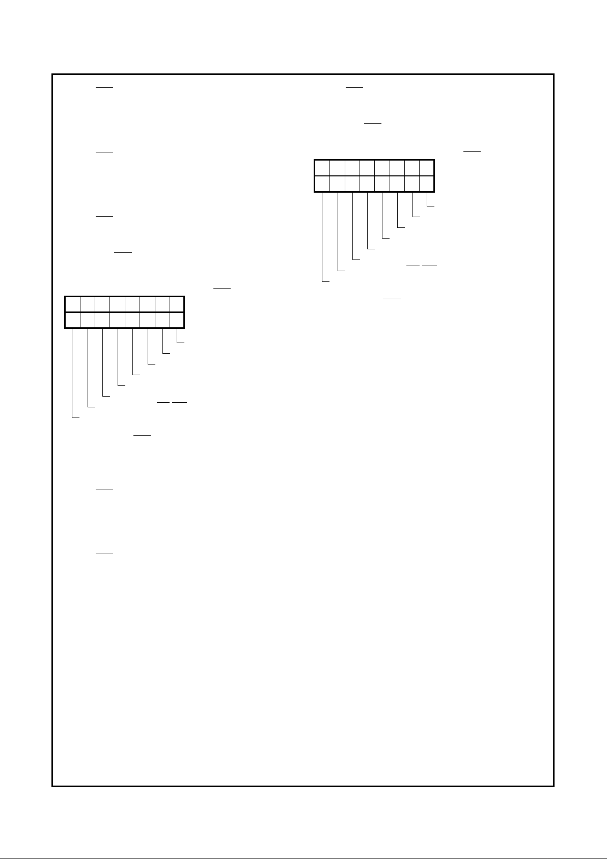
40
Configuration
www.national.com
2.10.5 CS1 Base Address MSB Register, Second
Level Index 04h
This read/write register is reset by hardware to 00h. Same
as Plug and Play ISA base address register at index 60h.
See Table 2-7 on page 28.
2.10.6
CS1 Base Address LSB Register, Second Level
Index 05h
This read/write register is reset by hardware to 00h. Same
as Plug and Play ISA base address register at index 61h.
See Table 2-7 on page 28.
2.10.7
CS1 Configuration Register, Second Level
Index 06h
This read/write register is reset by hardware to 00h. It functions like the CS0 Configuration Register described in Section 2.10.3.
FIGURE 2-15.
CS1 Configuration Register Bitmap
2.10.8 Reserved, Second Level Index 07h
Attempts to access this register produce undefined results.
2.10.9 CS2 Base Address MSB Register, Second
Level Index 08h
This read/write register is reset by hardware to 00h. It functions like the Plug and Play ISA base address register at index 60h. See Table 2-7 on page 28.
2.10.10
CS2 Base Address LSB Register, Second Level
Index 09h
This read/write register is reset by hardware to 00h. It functions like the Plug and Play ISA base address register at index 61h. See Table 2-7 on page 28.
Mask Address Pins A11-A0
76543210
Reset
Required
00000000
Second Level
Register,
Mask Address Pin A3
CS1 Configuration
Mask Address Pin A1
Mask Address Pin A2
Assert Chip Select Signal on Read
Mask Address Pin A0
Unaffected by
RD/WR
Assert Chip Select Signal on Write
Index 06h
2.10.11
CS2 Configuration Register, Second Level
Index 0Ah
This read/write register is reset by hardware to 00h. It functions like the CS0 Configuration register.
FIGURE 2-16.
CS2 Configuration Register Bitmap
2.10.12 Reserved, Second Level Indexes 0Bh-0Fh
Attempts to access these registers produce undefined results.
2.10.13 Not Accessible, Second Level Indexes 10h-FFh
Not accessible because bits 7-4 of the Index register are 0.
Mask Address Pins A11-A0
76543210
Reset
Required
00000000
Second Level
Register,
Mask Address Pin A3
CS2 Configuration
Mask Address Pin A1
Mask Address Pin A2
Assert Chip Select Signal on Read
Mask Address Pin A0
Unaffected by
RD/WR
Assert Chip Select Signal on Write
Index 0Ah
Page 41

41
Configuration
www.national.com
2.11 CARD CONTROL REGISTER BITMAPS
76543210
Reset
Required
00000011
00000011
SID (In PC87307)
Index 20h
Register,
Chip ID
Revision ID
76543210
Reset
Required
11110011
11110011
SID (In PC97307)
Index 20h
Register,
Chip ID
ZWS Enable
General Purpose Scratch Bits
76543210
Reset
Required
0x10x000
SuperI/O Configuration 1
Index 21h
Register,
PC-AT or PS/2 Drive Mode Select
CSOUT or CS0 Select
Reserved
Lock Scratch Bit
X-Bus Data Buffer (XDB) Select
BADDR1 and BADDR0
GPIO Bank Select
76543210
Reset
Required
xx000000
SuperI/O Configuration 2
Index 22h
Register,
GPIO21, IRSL2, ID2 or ISL0 Pin Select
GPIO22 or
POR Select
GPIO20 or IRSL1 Pin Select
GPIO17 or WDO Pin Select
Index of a Programmable
Read Only
76543210
Reset
Required
00000000
0000
Programmable Chip Select
Index 23h
Configuration Index
Chip Select Configuration
Register
Register,
Data in a Programmable
76543210
Reset
Required
00000000
Programmable Chip Select
Index 24h
Configuration Data
Chip Select Configuration
Register
Register,
76543210
Reset
Required
xxxxxxxx
SRID (in PC97307 only)
Index 27h
Register,
Chip Revision ID
KBC Clock Source
76543210
Reset
Required
00000010
SuperI/O KBC
Index F0h
Configuration
Reserved
Register,
Page 42

42
Configuration
www.national.com
TRI-STATE Control
Four Drive Control
76543210
Reset
Required
00000100
SuperI/O FDC
Index F0h
Configuration
Reserved
Register,
DENSEL Polarity Control
TDR Register Mode
Drive 0 ID
Reserved
76543210
Reset
Required
00000000
Index F1h
Drive ID Register,
Drive 1 ID
TRI-STATE Control
Parallel Port Mode Select
76543210
Reset
Required
01001111
Index F0h
Configuration Register,
PP of PnP ISA Resource Data
SuperI/O Parallel Port
Clock Enable
Reserved
Configuration Bits within the Parallel Port
TRI-STATE Control for
Bank Select Enable
76543210
Reset
Required
00000000
Index F0h
Configuration Register,
Ring Detection on RI Pin
SuperI/O UART1,2
Power Mode Control
Busy Indicator
Reserved
UART Pins
Mask Address Pins A11-4
76543210
Reset
Required
00000000
Second Level
Register,
Mask Address Pin A3
CS0 Configuration
Mask Address Pin A1
Mask Address Pin A2
Assert Chip Select Signal on Read
Mask Address Pin A0
Unaffected by
RD/WR
Assert Chip Select Signal on Write
Index 02h
Mask Address Pins A11-4
76543210
Reset
Required
00000000
Second Level
Register,
Mask Address Pin A3
CS1 Configuration
Mask Address Pin A1
Mask Address Pin A2
Assert Chip Select Signal on Read
Mask Address Pin A0
Unaffected by
RD/WR
Assert Chip Select Signal on Write
Index 06h
Mask Address Pins A11-4
76543210
Reset
Required
00000000
Second Level
Register,
Mask Address Pin A3
CS2 Configuration
Mask Address Pin A1
Mask Address Pin A2
Assert Chip Select Signal on Read
Mask Address Pin A0
Unaffected by
RD/WR
Assert Chip Select Signal on Write
Index 0Ah
Page 43

43
Keyboard (and Mouse) Controller (KBC) (Logical Devices 0 and 1)
www.national.com
FIGURE 3-1. KBC System Functional Block Diagram
KBDATInterrupt Matrix KBCLK MDAT MCLK
Program
ROM
2 K x 8
Data
RAM
256 x 8
(including
registers
and stack)
I/O Port 2
8-Bit
Serial Open-Collector
Drivers
8-Bit Timer
DBBOUT
DBBINSTATUS
RD WR
P21-20
P27, P26, P23, P22
TEST1
TEST0
D7-0
Timer
8-Bit Internal Bus
Program
Address
IBF
I/O Interface
PC87307/PC97307 Interface
I/O PORT 1
8-Bit
P11,10
P17, P16, P12
P24
P25
8-Bit
CPU
To PnP
A2
or Counter
Overflow
3.0 Keyboard (and Mouse) Controller
(KBC) (Logical Devices 0 and 1)
The Keyboard Controller (KBC) is a functionally independent programmable device controller. It is implemented
physically as a single hardware module on the part multi-I/O
chip and houses two separate logical devices: a keyboard
controller and a mouse controller.
The KBC accepts user input from the keyboard or mouse,
and transfers this input to the host PC via the common
PC87307/PC97307-PC interface.
The KBC is functionally equivalent to the industry standard
8042A keyboard controller, which may serve as a detailed
technical reference for the KBC.
The KBC is delivered preprogrammed with customer-supplied code. KBC firmware code is identical to 8042 code,
and to code of the keyboard controller of the PC87323VUL
chip. The PC87323VUL is recommended as a development
platform for the KBC since it uses identical code and includes an internal program RAM that enables software development
3.1 SYSTEM ARCHITECTURE
The KBC is a general purpose microcontroller, with an 8-bit
internal data bus. See Figure 3-1. It includes the following
functional blocks:
Serial Open-Collector Drivers: Four open-collector bi-di-
rectional serial lines enable serial data exchange with
the external devices (keyboard and mouse) using the
PS/2 protocol.
Program ROM: 2 Kbytes of ROM store program machine
code in non-erasable memory. The code is copied to this
ROM during manufacture, from customer-supplied code.
Data RAM: 256 bytes of Data RAM enables run-time inter-
nal data storage, and includes an 8-level stack and 16
8-bit registers.
Timer/Counter: An internal 8-bit timer/counter can count
external events or pre-divided system clock pulses. An internal time-out interrupt may be generated by this device.
I/O Ports: Two 8-bit ports (Port 1 and Port 2) serve various
I/O functions. Some are for general purpose use, others
are utilized by the KBC firmware as shown in Figure 3-1.
Page 44

44
Keyboard (and Mouse) Controller (KBC) (Logical Devices 0 and 1)
www.national.com
FIGURE 3-2. System Interfaces
PC
Chipset
SA15-0
PC87307/PC97307
XD7-0
MR
A15-0
D7-0
AEN
RD
WR
KBC IRQ
Mouse IRQ
KBC
KBCLK
KBDAT
TEST0
P10
Keyboard Clock
Keyboard Data
MCLK
MDAT
TEST1
P11
Mouse Clock
Mouse Data
P26
P27
P23
P22
STATUS
DBBIN
DBBOUT
Plug and
Play
Matrix
P24
P25
P16
P17
P20
P21
P12
Internal Interface Bus
IRQn
3.2 FUNCTIONAL OVERVIEW
The KBC supports two external devices — a keyboard and
a mouse. Each device communicates with the KBC via two
bidirectional serial signals. Five additional external generalpurpose I/O signals are provided.
KBC operation involves three signal interfaces:
• External I/O interface
• Internal KBC - PC87307/PC97307 interface
• PC87307/PC97307 - PC chip set interface.
These system interfaces are shown in Figure 3-2.
The KBC uses two data registers (for input and output) and
a status register to communicate with the part central system. Data exchange between these units may be based on
programmed I/O or interrupt-driven.
The KBC has two internal interrupts: the Input Buffer Full
(IBF) interrupt and Timer Overflow interrupt (see Figure
3-1). These two interrupts can be independently enabled or
disabled by KBC firmware. Both are disabled by a hard reset. These two interrupts only affect the execution flow of
the KBC firmware, and have no connection with the external
interrupts requested by this logical device.
The KBC can generate two external interrupt requests.
These request signals are controlled by the KBC firmware
which generates them by manipulating I/O port signals. See
Section 3.3.2.
The part supports the KBC and handles interactions with
the PC chip set. In addition to data transfer, these interactions include KBC configuration, activation and status monitoring. The part interconnects with the host via one
interface that is shared by all chip devices
The KBC clock is generated from the main clock of the chip,
which may come from an external clock source or from the
internal frequency multiplier. (See Sections 3.3 and 3-4.)
The KBC clock rate is configured by the SuperI/O (SIO)
Configuration Registers.
3.3 DEVICE CONFIGURATION
The KBC hardware contains two logical devices—the KBC
(logical device 0) and the mouse (logical device 1).
3.3.1 I/O Address Space
The KBC has two I/O addresses and one IRQ line (KBC
IRQ) and can operate without the companion mouse.
The mouse cannot operate without the KBC device. It has
one IRQ line (mouse IRQ) but has no I/O address. It utilizes
the KBC I/O addresses.
3.3.2 Interrupt Request Signals
The KBC IRQ and Mouse IRQ interrupt request signals are
identical to (or functions of) the P24 and P25 signals of the
8042. These interrupt request signals are routed internally
to the Plug and Play interrupt Matrix and may be routed to
user-programmable IRQ pins. Each logical device is independently controlled.
The Interrupt Select registers (index 70h for each logical device) select the IRQ pin to which the corresponding interrupt
request is routed. The interrupt may also be disabled by not
routing its request signal to any IRQ pin.
Bit 0 of the Interrupt Type registers (index 71h for each logical device) determines whether the interrupts are passed
(bit 0 = 0) or latched (bit 0 = 1). If bit 0 = 0, interrupt request
signals (P24 and P25) are passed directly to the selected
IRQ pin. If bit 0 = 1, interrupt request signals that become
active are latched on their rising edge, and held until read
from the KBC output buffer (port 60h).
Figure 3-3 illustrates the internal interrupt request logic.
Page 45

45
Keyboard (and Mouse) Controller (KBC) (Logical Devices 0 and 1)
www.national.com
Note:
The EN FLAGS command (used for routing OBF and
IBF onto P24 and P25 in the 8042) causes unpredictable results and should not be issued.
3.3.3 KBC Clock
The KBC clock frequency is selected by the SuperI/O KBC
Configuration Register at index F0h of logical device 0 to be
either 8, 12 or 16 MHz. 16 MHz is not available when the
clock source on pin X1 is 24 MHz. This clock is generated
from a 32.768 KHz crystal connected to pins X1C and X2C,
or from either a 24 MHz or a 48 MHz clock input at pin X1.
See “SuperI/O KBC Configuration Register, Index F0h” on
page 36, Figures 3-4 and 3-5. The clock source and frequency may only be changed when the KBC is disabled.
For details regarding the configuration of each device, refer
to Tables 2-12 and 2-13 starting on page 30.
FIGURE 3-5. External Clock Connection
PC87307/PC97307
X1
+V
CC
External
Clock
Standard or
Open-Collector
TTL Driver
FIGURE 3-3. Interrupt Request Logic
FIGURE 3-4. Instruction Timing
From Mouse IRQ
A15-0
AEN
Address
Decoder
MR
Port 60
Read
Mouse IRQ Feedback
From KBC IRQ
PR
Q
D
CLR
“1”
0
1
MUX
Interrupt
KBC IRQ Feedback
CLK
Interrupt Enable
A15-0
AEN
RD
Address
Decoder
Port 60
Read
Interrupt Enable
MR
RD
(1 = Latch)
Interrupt
(0 = Invert)
To Selected KBC IRQ Pin
Type
Polarity
0
1
MUX
Plug and
Play Matrix
PR
Q
D
CLR
“1”
0
1
MUX
Interrupt
CLK
(1 = Latch)
Interrupt
(0 = Invert)
To Selected Mouse IRQ Pin
Type
Polarity
0
1
MUX
Plug and
Play Matrix
S1 S2 S3 S4 S5 S1
1 Instruction Cycle = 15 Clock Cycles
KBC CLK
Page 46

46
Keyboard (and Mouse) Controller (KBC) (Logical Devices 0 and 1)
www.national.com
External
TEST1
3-State
5-Cycle
32-Bit
Timer
Prescaler
8-Bit Timer
or Counter
Overflow
Flag
Stop
Counter
Counter
Timer
Counter
Interrupt
(MCLK)
Frequency
X1
X1C
X2C
External
32768 Hz
Crystal
External Event Input
24 or 48 MHz
Clock
÷
KBC Clock
Clock
Select
48 MHz
2 or 3
÷ 2
Select
Frequency
Multiplier
(1465)
Source
FIGURE 3-6. Timing Generation and Timer Circuit
3.3.4 Timer or Event Counter
The keyboard controller includes an 8-bit counter, which
can be used as a timer or an event counter, as selected by
the firmware.
Timer Operation
When the internal clock is chosen as the counter input, the
counter functions as a timer. The clock fed to the timer consists of the KBC instruction cycle clock, divided by 32. (See
Figures 3-4 and 3-6.) The divisor is reset only by a hardware
reset or when the timer is started by an STRT T instruction.
The timer counts up from a programmable initial value and
sets an overflow flag when it overflows. This flag may be
tested, or may be set up to generate an overflow interrupt.
Refer to the 8042 or PC87323VUL instruction set for details.
Event Counter Operation
When the clock input of the counter is switched to the external input (MCLK), it becomes an event counter. The falling
edge of the signal on the MCLK pin causes the counter to
increment. Timer Overflow Flag and Timer interrupt operate
as in the timer mode.
3.4 EXTERNAL I/O INTERFACES
The PC chipset interfaces with the part as illustrated in Figure 3-2 on page 44.
All data transactions between the KBC and the PC chipset
are handled by the part.
The part decodes all I/O device chip-select functions from
the address bus. The KBC chip-select codes are, traditionally, 60h or 64h, as described in Table 3-1. (These addresses are user-programmable.)
The external interface includes two sets of signals: the keyboard and mouse interface signals, and the general-purpose I/O signals.
3.4.1 Keyboard and Mouse Interface
Four serial I/O signals interface with the external keyboard
and mouse. These signals are driven by open-collector drivers with signals derived from two I/O ports residing on the
internal bus. Each output can drive 16 mA, making them
suitable for driving the keyboard and mouse cables. The
signals are named KBCLK, KBDAT, MCLK and MDAT, and
they are the logical complements of P26, P27, P23 and
P22, respectively.
TEST0 and TEST1 are dedicated test pins, internally connected to KBCLK and MCLK, respectively, as shown in Figures 3-1 and 3-2. These pins may be used as logical
conditions for conditional jump instructions, which directly
check the logical levels at the pins.
KBDAT and MDAT are connected to pins P10 and P11, respectively.
MCLK also provides input to the event counter.
3.4.2 General Purpose I/O Signals
The P12, P16, P17, P20 and P21 general purpose I/O signals interface to two I/O ports (port1 and port2). P12, P16
and P17 are mapped to port 1 and P20 and P21 are
mapped to port 2.
P12, P16 and P17 are driven by quasi-bidirectional drivers.
(See Figure 3-7.) These signals are called quasi-bidirectional because the output buffer cannot be turned off (even
when the I/O signal is used for input).
During output, a 1 written to output is strongly pulled up for
the duration of a (short) write pulse, and thereafter maintained by a high impedance “weak” active pull-up (implemented by a degenerated transistor employed as a
switchable pull-up resistor). A series resistor to those port
lines used for input is recommended to limit the surge current during the strong pull-up. See Figure 3-8.
Page 47

47
Keyboard (and Mouse) Controller (KBC) (Logical Devices 0 and 1)
www.national.com
FIGURE 3-7. Quasi-Bidirectional Driver
FIGURE 3-8. Current Limiting Resistor
MR
Port
Write
Internal Bus
PORT
F/F
ORL, ANL
+VCC
PAD
IN
Q1
Q2
Q3
D
P
Q
Q
PC87307/PC97307
Port Pin
Port Pin
R
R
R: current limiting resistor
A small-value series current limiting
resistor is recommended when
port pins are used for input.
100 500Ω–
100 500Ω–
If a 1 is asserted, an externally applied signal may pull down
the output. Therefore, input from this quasi-bidirectional circuit can be correctly read if preceded by a 1 written to output.
P20 and P21 are driven by open-drain drivers.
When the KBC is reset, all port data bits are initialized to 1.
3.5 INTERNAL KBC - PC87307/PC97307 INTERFACE
The KBC interfaces internally with the part via three registers: an input (DBBIN), output (DBBOUT) and status (STATUS) register. See Figure 3-1 on page 43 and Table 3-1.
TABLE 3-1. System Interface Operations
RD WR
Default
Addresses
Operation
0 1 60h
Read DBBOUT
1 0 60h
Write DBBIN, F1 Clear (Data)
0 1 64h
Read STATUS
1 0 64h
Write DBBIN, F1 Set (Command)
Table 3-1 illustrates the use of address line A2 to differentiate between data and commands. The device is selected by
chip identification of default address 60h (when A2 is 0) or
64h (when A2 is 1). After reset, these addresses can be
changed by software.
3.5.1 The KBC DBBOUT Register, Offset 60h,
Read Only
The DBBOUT register transfers data from the keyboard
controller to the part. It is written to by the keyboard controller and read by the part for transfer to the PC. The PC may
be notified of the need to read data from the KBC by an interrupt request or by polling the Output Buffer Full (OBF) bit
(bit 0 of the KBC STATUS register described in Section
3.5.3 on page 48).
3.5.2 The KBC DBBIN Register, Offset 60h (F1 Clear)
or 64h (F1 Set), Write Only
The DBBIN register transfers data from the part system to
the keyboard controller. (This transaction is transparent to
the user, who should program the device as if direct access
to the registers were in effect.)
When data is received in this manner, an Input Buffer Full
(IBF) internal interrupt may be generated in the KBC, to deal
with this data. Alternatively, reception of data in this manner
can be detected by the KBC polling the Input Buffer Full bit
(IBF, bit 1 of the KBC STATUS register).
Page 48

48
Keyboard (and Mouse) Controller (KBC) (Logical Devices 0 and 1)
www.national.com
3.5.3 The KBC STATUS Register, Offset 64h,
Read Only
The STATUS register holds information regarding the system interface status. Figure 3-9 shows the bit definition of
this register. This register is controlled by the KBC firmware
and hardware, and is read-only for the system.
FIGURE 3-9. KBC STATUS Register Bitmap
Bit 0 - OBF, Output Buffer Full
A 1 indicates that data has been written into the DBBOUT register by the KBC. It is cleared by a system
read operation from DBBOUT.
Bit 1 - IBF, Input Buffer Full
When a write operation is performed by the host system,
this bit is set to 1, which may be set up to trigger the IBF
interrupt. Upon executing an IN A, DBB instruction, it is
cleared.
Bit 2 - F0, General Purpose Flag
A general purpose flag that can be cleared or toggled by
the keyboard controller firmware.
Bit 3 - F1, Command/Data Flag
This flag holds the state of address line A2 while a write
operation is performed by the host system. It distinguishes between commands and data from the host
system. In this device, a write with A2 = 1 (hence F1 =
1) is defined as a command, and A2 = 0 (hence F1 = 0)
is data.
Bits 7-4, General Purpose Flags
These flags may be modified by KBC firmware.
3.6 INSTRUCTION TIMING
The KBC clock is first divided by 3 to generate the state timing, then by 5 to generate the instruction timing. Thus each
instruction cycle consists of five states and 15 clock cycles.
Most keyboard controller instructions require only one instruction cycle, while some require two cycles. Refer to the
8042 or PC87323VUL instruction set for details.
76543210
Reset
OBF Output Buffer Full
IBF Input Buffer Full
F0 General Purpose Flag
F1 Command or Data Flag
General Purpose
Flags
KBC Status Register
Offset 64h
00000000
Read Only
Page 49

49
Real-Time Clock (RTC) and Advanced Power Control (APC) (Logical Device 2)
www.national.com
4.0 Real-Time Clock (RTC) and
Advanced Power Control (APC)
(Logical Device 2)
The RTC logical device contains two major functions: the
Real-Time Clock (RTC) and Advanced Power Control
(APC).
The RTC is a timekeeping module that supplies a time-ofday clock and a multi-century calendar in various formats. It
provides alarm facilities and three programmable timer interrupts. It continues valid timekeeping and maintains RAM
contents during power down by utilizing external battery
backup.
Additional features of the RTC include Advanced Power
Control (APC), a century timekeeping storage byte, full Plug
and Play support, additional battery-backed RAM and RAM
lock schemes, and additional power management options.
The APC function adds the ability of automatic PC system
power-up in response to external events. This enables efficient use of the PC system in applications such as voice answering machines or fax receivers, which are typically
powered up at all times.
The APC also enables a controlled power-down sequence
when switched off by the user. The APC function does not
replace the power management abilities of various modules−it adds power management ability to the PC host system.
RTC software is compatible with the DS1287 and
MC146818 clock chips. (The only difference is that Port 70
is read/write in this module, and is write-only in the DS1287
and MC146818.)
Battery-Backed Register Banks and RAM
The RTC and APC module has three battery-backed register banks. Two are used by the logical units themselves.
The host system uses the third for general purpose batterybacked storage.
Battery-backup power enables information retention during
system power down.
The banks are:
• Bank 0 - General Purpose Register Bank
• Bank 1 - RTC Register Bank
• Bank 2 - APC Register Bank
The memory maps and register content for each of the three
banks is illustrated in Section 4.7 on page 64.
The lower 64-byte locations of the three banks are shared.
The first 14 bytes store time and alarm data and contain
control registers. The next 50 bytes are general purpose
memory.
The upper 64 bytes of bank addresses are utilized as follows:
• Bank 0 supplies an additional 64 bytes of memory
backed RAM.
• Bank 1 uses the upper 64 bytes for functions specific
to the RTC activity and for addressing Upper RAM.
• Bank 2 uses the upper 64 bytes for functions specific
to the APC activity.
Registers with reserved bits should be written in “ReadModify-Write” method.
RTC Control Register A (CRA) selects the active bank according to the value of bits 6-4 (DV2-0). (See Table 4-3 on
page 53.)
All register locations within the device are accessed by the
RTC Index and Data registers (at base address and base
address+1). The Index register points to the register location being accessed, and the Data register contains the
data to be transferred to or from the location. An additional
128 bytes of battery-backed RAM (also called upper RAM)
may be accessed via a second level address. The second
level uses the upper RAM Index register at index 50h of
bank 1 and the upper RAM Data register at index 53h of
bank 1.
Access to the three register banks and RAM may be locked.
For details see “RAM Lock Register (RLR), Index 47h” on
page 62.
4.1 RTC OPERATION OVERVIEW
The control registers listed in Table 4-1 control all RTC operation. These registers appear in all the RTC register
banks. See Section 4.7 on page 64.
TABLE 4-1. RTC Control Registers
RTC configuration registers within the part store the settings for all interface, configuration and power management
options. These registers are described in detail in Section
2.3 on page 26.
The RTC employs an external crystal connected to an inter-
nal oscillator circuit or an optional external clock input, as
the basic clock for timekeeping.
Local battery-backed RAM serves as storage for all timekeeping functions.
4.1.1 RTC Hardware and Functional Description
Bus Interface
The RTC function is initially mapped to the default I/O locations at indexes 70h (Index) and 71h (data) within the part.
These locations may be reassigned, in compliance with the
Plug and Play requirements. See Section 2.2 on page 25.
External Clock and Timing Generation
The RTC can use one of the following timekeeping input
clock options:
• A 32768 Hz crystal connected externally at the X1C
and X2C pins completes an oscillator circuit and generates the 32768 Hz input clock. (See “Oscillator Internal and External Circuitry” on page 50.)
Index Name Description
0Ah CRA RTC Control Register A
0Bh CRB RTC Control Register B
0Ch CRC RTC Control Register C
0Dh CRD RTC Control Register D
Page 50

50
Real-Time Clock (RTC) and Advanced Power Control (APC) (Logical Device 2)
www.national.com
• An external clock may be connected to pin X1C.
The time generation function divides the 32.768 KHz by 2
15
to derive a 1 Hz signal which serves as the input for timekeeping functions. Bits 6-4 of RTC Control Register A
(CRA) control the activity and location of the divider chain in
memory. Bits 3-0 of the CRA register select one of fifteen
taps from the divider chain to be used as a periodic interrupt. See Section “RTC Control Register A (CRA), Index
0Ah” on page 52 for a description of divider configurations
and rate selections.
The divider chain is reset to 0 by bits 6-4 of the CRA register. An update occurs 500 msec after the divider chain is activated by setting normal operational mode (bits 6-4 of CRA
= 010). The periodic flag becomes active one half of the programmed period after the divider chain is activated.
Figure 4-1 illustrates the internal and external circuitry that
comprise the oscillator.
FIGURE 4-1. Oscillator Internal and External Circuitry
This oscillator is active under normal power or during power
down. It stops only in the event of a power failure with the
oscillator disabled (see “Oscillator Activity” on page 52), or
when battery backup power drops below two volts.
If oscillator input is from an external source, input should be
driven rail to rail and should have a nominal 50% duty cycle.
In this case, oscillator output X2C should be disabled.
External capacitor values should be chosen to provide the
manufacturer’s specified load capacitance for the crystal
when combined with the parasitic capacitance of the trace,
socket, and package, which can vary from 0 to 8 pF. The
rule of thumb in choosing these capacitors is:
C
L
= (C1 * C2) ÷ (C1 + C2) + C
PARASITIC
C2 > C1
C1 can be trimmed to achieve precisely 32768.0 Hz after insertion.
Start-up time for this oscillator may vary from two to seven
seconds due to the high Q of the crystal. The parameters
below describe the crystal requirements:
Parallel, resonant, tuning fork (N cut) or XY bar
Q ≥ 35000
Load Capacitance (C
L
) 9 to 13 pF
Accuracy and temperature coefficients are user defined.
20 MΩ
Internal
External
R
EXT
X1C
X2C
C1 C2
R
EXT
= 120 KΩ
C1 = 10 pF
C2 = 33 pF
C
PARASITIC
= 8 pF
4.1.2 Timekeeping
Time is kept in BCD or binary format as determined by bit 2
(DM) of Control Register B (CRB). Either 12 or 24 hour representation for the hours can be maintained as determined
by bit 1 of CRB. When changing formats, the time registers
must be re-initialized to the corresponding data format.
Daylight savings time and leap year exceptions are handled
by the timekeeping function. When bit 0 (the Daylight Saving Enable bit, DSE) of CRB is set to 1, time advances from
1:59:59 AM to 3:00:00 on the first Sunday in April, and
changes from 1:59:59 to 1:00:00 on the last Sunday of October. In leap years, February is extended to 29 days.
Updating
Timekeeping is performed by hardware, which updates a
pre-programmed time value once per second. The pre-programmed time values are written by the user to the following
locations:
The values for seconds, minutes, hours, day of week, date
of month, month and year are located in the common storage area in all three memory banks (See Table 4-6 on page
64). The century value is located in Bank 1 (See Table 4-8
on page 65).
Users must ensure that reading or writing to the time storage locations does not coincide with a system update of
these locations, which would cause invalid and unpredictable results.
There are several ways to avoid this contention. Four options follow:
Method 1 - Set the SET bit (bit 7 of the CRB register) to 1.
This takes a “snapshot” of the internal time registers and
loads it into the user copy. If user copy registers have
been updated, the user copy updates the internal registers when the SET bit goes from 1 to 0. This mechanism
enables loading new time parameters into the RTC.
Method 2 - Access after detection of an Update-Ended in-
terrupt.
This implies that an update has just completed and
there are 999 msec remaining until the next occurrence.
Method 3 - Poll Update-In-Progress (UIP) (bit 7 in Control
Register A).
The update occurs 244 µsec after the update-in-
progress bit goes high. Therefore if a 0 is read, there is
a minimum of 244µs in which the time is guaranteed to
remain stable.
Method 4 - Use a periodic interrupt to determine if an up-
date cycle is in progress.
The periodic interrupt is first set to a desired period. Pe-
riodic interrupt appearance then indicates there is a period of (Period of periodic interrupt ÷ 2 + 244 µsec)
remaining until another update occurs.
Page 51

51
Real-Time Clock (RTC) and Advanced Power Control (APC) (Logical Device 2)
www.national.com
Alarms
The timekeeping function may generate an alarm when the
current time reaches a stored alarm time. After each RTC
time update, the seconds, minutes, and hours storage locations are compared with the seconds, minutes and hours in
the alarm storage locations. If equal, the alarm flag is set in
Control Register C (CRC). If the Alarm Interrupt Enable
(AIE) bit is set in Control Register B (CRB), then setting the
Alarm Flag (AF) in CRC generates the
IRQ internal interrupt
request (
IRQ = 0).
Any alarm location, i.e., seconds, minutes or hours, may be
set to a “Don’t Care” state by setting bits 7,6 to 11. (This value is unused for either BCD or binary time codes.) This results in periodic alarm activation at an increased rate whose
period is that of the Don’t Care location, e.g., if the hours location is set to 11, the alarm will be activated every hour.
The seconds, minutes and hours alarm registers are shared
with the wake-up function.
4.1.3 Power Supply
The host PC and part power is supplied by the system power supply voltage, V
DD.
Figure 4-2 shows the power supplies of the part.
A stand-by voltage (V
CCH
) from the external AC power supply powers the RTC and APC under normal conditions. The
V
DD
voltage reaches the RTC/APC as a sense signal, to de-
termine the presence or absence of a valid V
DD
supply.
A battery backup voltage V
BAT
maintains RTC/APC time-
keeping and backup memory storage when the V
CCH
voltage is absent, due to power failure or disconnection of the
external AC input power supply.
The APC function produces the
ONCTL signal, which con-
trols the V
DD
power supply voltage. (See Section 4.4.1 on
page 58.)
To ensure proper operation, a 500 mV differential is needed
between V
CCH
and V
BAT
.
Figure 4-3 represents a typical battery configuration. No external diode is required to meet the UL standard, due to the
internal serial resistor.
FIGURE 4-2. PC87307/PC97307 Power Supplies
FIGURE 4-3. Typical Battery Configuration
Host PC
Power Supply Module
Backup
External AC Power
V
DD
V
CCH
VDD Power
V
DD
Sense
V
CCH
Power
V
BAT
Power
ONCTL
RTC
and
APC
Modules
PC87307/
Battery
PC97307
PC87307/
V
BAT
0.1µ
1µ
F
F
V
CCH
V
CCH
PC97307
Page 52

52
Real-Time Clock (RTC) and Advanced Power Control (APC) (Logical Device 2)
www.national.com
System Bus Lockout
As the RTC switches to battery power all, input signals are
locked out so that the internal registers can not be modified
externally.
Power Up Detection
When system power is restored after a power failure, the
power failure lock condition continues for a delay of 62
msec (minimum) to 125 msec (maximum) after the RTC
switches from battery power to system power.
The power failure lock condition is switched off immediately
in the following situations:
• If the Divider Chain Control bits (DV2-0, bits 6-4 in Con-
trol Register A) specify any mode other than 010, 100 or
011, all input signals are enabled immediately upon detection of system voltage above that of the battery voltage.
• When battery voltage is below 1 volt and MR is 1, all in-
put signals are enabled immediately upon detection of
system voltage above that of battery voltage. This also
initializes registers at indexes 00h through 0Dh.
• If the VRT bit (bit 7 in Control Register D) is 0, all input
signals are enabled immediately upon detection of system voltage above that of battery voltage.
Oscillator Activity
The RTC internal oscillator circuit is active whenever power
is supplied to the RTC with the following exceptions:
• Software wrote 000 or 001 to the Divider Chain Con-
trol bits (DV2-0), i.e., bits 6-4, of Control Register A,
and the RTC is supplied by V
BAT,
or
• The RTC is supplied by V
BAT
and the VRT bit of Con-
trol Register D is 0.
These conditions disables the oscillator.
When the oscillator becomes inactive, the APC is disabled.
4.1.4 Interrupt Handling
The RTC logic device has a single Interrupt Request line,
IRQ, which handles three interrupt conditions. The Periodic,
Alarm, and Update-Ended interrupts are generated (
IRQ is
driven low) if the respective enable bits in Control Register
B are set when an interrupt event occurs.
Reading RTC Control Register C (CRC) clears all interrupt
flags. Thus, it is recommended that when multiple interrupts
are enabled, the interrupt service routine should first read
and store the CRC register, then deal with all pending interrupts by referring to this stored status.
If an interrupt is not serviced before a second occurrence of
the same interrupt condition, the second interrupt event is
lost. Figure 4-5 illustrates interrupt and status timing in the
part.
4.2 THE RTC REGISTERS
The RTC registers can be accessed at any time during nonbattery backed operation. These registers cannot be written
to before reading the VRT bit (bit 7 of the “RTC Control Register D (CRD), Index 0Dh” on page 55), thus preventing
bank selection and other functions. The user must read the
VRT bit as part of the startup activity.
These registers are listed in Table 4-1 and described in detail in the sections that follow.
4.2.1 RTC Control Register A (CRA), Index 0Ah
The CRA register controls periodic interrupt rate selection
and bank selection.
FIGURE 4-4. CRA Register Bitmap
Bits 3-0 - Periodic Interrupt Rate Select (RS3-0)
These read/write bits select one of fifteen output taps
from the clock divider chain to control the rate of the periodic interrupt. See Table 4-2 and Figure 4-5.
Master reset does not affect these bits.
Bits 6-4 - Divider Chain Control (DV2-0)
These read/write bits control the configuration of the divider chain for timing generation and memory bank selection, as shown in Table 4-3.
Master reset does not affect these bits.
Bit 7 - Update in Progress (UIP)
This read only bit is not affected by reset.
0 - An update will not occur within the next 244 µsec.
Bit 7 (the SET bit) of Control Register B (CRB) is 1.
1 - Timing registers are updated within 244 µsec.
RS2
DV0
DV2
UIP
76543210
Index 0Ah
Power-Up
Required
RTC Control
00000100
RS0
RS3
DV1
RS1
(CRA)
Reset
Register A
Page 53

53
Real-Time Clock (RTC) and Advanced Power Control (APC) (Logical Device 2)
www.national.com
A-B Update In Progress (UIP) bit high before update occurs = 244 µsec
D-C Periodic interrupt to update = Period (periodic int) / 2 + 244 µsec
C-E Update to Alarm Interrupt = 30.5 µs
UIP Update In Progress status bit
UF Update-Ended Interrupt Flag (Update-Ended Interrupt if enabled)
PF Periodic Flag (Periodic Interrupt if enabled)
AF Alarm Flag (Alarm Interrupt if enabled)
Flags (and IRQ) are reset at the conclusion of Control Register C (CRC) read or by reset.
UIP bit of CRA
UF bit of CRC
PF bit of CRC
AF bit of CRC
A
B
C
D
E
FIGURE 4-5. Interrupt/Status Timing
TABLE 4-2. Periodic Interrupt Rate Encoding
RS3-0
3 2 1 0
Periodic Interrupt Rate
0 0 0 0 none
0 0 0 1 3.90625 msec
0 0 1 0 7.8125 msec
0 0 1 1 122.070 µsec
0 1 0 0 244.141 µsec
0 1 0 1 488.281 µsec
0 1 1 0 976.562 µsec
0 1 1 1 1.953125 msec
1 0 0 0 3.90625 msec
1 0 0 1 7.8125 msec
1 0 1 0 15.625 msec
1 0 1 1 31.25 msec
1 1 0 0 62.5 msec
1 1 0 1 125 msec
1 1 1 0 250 msec
1 1 1 1 500 msec
TABLE 4-3. Divider Chain Control and Bank Selection
a. The oscillator stops in this case only in the
event of a power failure.
DV2-0
6 5 4
Selected
Bank
Configuration
0 0 0 Bank 0
Oscillator Disabled
a
0 0 1 Bank 0
Oscillator Disabled
a
0 1 0 Bank 0 Normal Operation
0 1 1 Bank 1 Normal Operation
1 0 0 Bank 2 Normal Operation
1 0 1 Undefined Test
1 1 0 Bank 0 Divider Chain Reset
1 1 1 Bank 0 Divider Chain Reset
Page 54

54
Real-Time Clock (RTC) and Advanced Power Control (APC) (Logical Device 2)
www.national.com
4.2.2 RTC Control Register B (CRB), Index 0Bh
This register enables the selection of various time and date
options, as well as the use of interrupts.
FIGURE 4-6. CRB Register Bitmap
Bit 0 - Daylight Savings Enable (DSE)
Master reset does not affect this read/write bit.
0 - Disables the daylight savings feature.
1 - Enables daylight savings feature, as follows:
In the spring, time advances from 1:59:59 to
3:00:00 on the first Sunday in April.
In the fall, time returns from 1:59:59 to 1:00:00 on
the last Sunday in October.
Bit 1 - 24 or 12 Hour Mode
This is a read/write bit that is not affected by reset.
0 - Enables 12 hour format.
1 - Enables 24 hour format.
Bit 2 - Data Mode (DM)
This is a read/write bit that is not affected by reset.
0 - Enables BCD format.
1 - Enables binary format.
Bit 3 - Unused
This bit is defined as “Square Wave Enable” by the
MC146818 and is not supported by the RTC. This bit is
always read as 0.
Bit 4 - Update-Ended Interrupt Enable (UIE)
Master reset forces this read/write bit to 0.
0 - Disables generation of the Update-Ended interrupt.
1 - Enables generation of the Update-Ended interrupt.
This interrupt is generated at the time an update
occurs.
Bit 5 - Alarm Interrupt Enable (AIE)
Master reset forces this read/write bit to 0.
0 - Disables generation of the alarm interrupt.
1 - Enables generation of the Alarm interrupt. The
alarm interrupt is generated immediately after a
time update in which the Seconds, Minutes, and
Hours time equal their respective alarm counterparts.
DM
UIE
AIE
PIE
SET
76543210
0000
DSE
24 or 12 Hour Mode
Unused
0
Index 0Bh
Power-Up
Required
RTC Control
(CRB)
Reset
Register B
Bit 6 - Periodic Interrupt Enable (PIE)
Master reset forces this read/write bit to 0.
0 - Disables generation of the Periodic interrupt.
1 - Enables generation of the Periodic interrupt. Bits 3-
0 of Control Register A (CRA) determine the rate of
the Periodic interrupt.
Bit 7 - Set Mode (SET)
Master reset does not affect this read/write bit.
0 - The timing updates occur normally.
1 - The user copy of time is “frozen”, allowing the time
registers to be accessed without regard for an occurrence of an update.
4.2.3 RTC Control Register C (CRC), Index 0Ch
This register indicates the status of interrupt request flags.
FIGURE 4-7. CRC Register Bitmap
Bits 3-0 - Reserved
These bits are reserved and always return 0000.
Bit 4 - Update-Ended Interrupt Flag (UF)
Master reset forces this read-only bit to 0. In addition,
this bit is reset to 0 when this register is read.
0 - No update has occurred since the last read.
1 - Time registers have been updated.
Bit 5 - Alarm Interrupt Flag (AF)
Master reset forces this read-only bit to 0.
0 - No alarm was detected since the last read.
1 - An alarm condition was detected. This bit is reset to
0 when this register is read.
Bit 6 - Periodic Interrupt Flag (PF)
Master reset forces this read-only bit to 0. In addition,
this bit is reset to 0 when this register is read.
0 - Indicates no transition occurred on the selected tap
since the last read.
1 - A transition occurred on the selected tap of the di-
vider chain.
UF
AF
PF
IRQF
76543210
0000000
0000
Reserved
Index 0Ch
Power-Up
Required
RTC Control
(CRC)
Reset
Register C
Page 55

55
Real-Time Clock (RTC) and Advanced Power Control (APC) (Logical Device 2)
www.national.com
Bit 7 - Interrupt Request Flag (IRQF)
This read-only bit is the inverse of the value on the
IRQ
output signal of the RTC/APC.
0 -
IRQ is inactive (high).
1 -
IRQ is active (low) and any of the following conditions exists: both PIE and PF are 1; both AIE and
AF are 1; both UIE and UF are 1. (PIE, AIE and
UIE are bits 6, 5 and 4, respectively of the CRB
register.)
4.2.4 RTC Control Register D (CRD), Index 0Dh
This register indicates the validity of the RTC RAM data.
FIGURE 4-8. CRD Bitmap
Bits 6-0 - Reserved
These bits are reserved and are always 0.
Bit 7 - Valid RAM and Time (VRT)
The VRT bit senses the voltage that feeds this logical
device (V
CCH
or V
BAT
) and indicates whether or not it
was too low since the last time this bit was read. If it was
too low, the RTC and RAM data are not valid.
This read-only bit is set to 1 when this register is read.
0 - The voltage that feeds the APC/RTC logical device
was too low.
1 - The RTC and RAM data are valid.
WARNING:
If V
CCH
ramps down at a rate exceeding 1 V/msec, it
may reset this bit.
VRT
76543210
00000000
0000000
Reserved
Index 0Dh
Power-Up
Required
RTC Control
(CRD)
Reset
Register D
4.3 APC OVERVIEW
Advanced Power Supply Control (APC) is implemented
within the RTC logical device. It enables the PC to power up
automatically, as required by specific conditions, or to power down in an orderly, controlled manner, replacing the
physical power supply On/Off switch.
The APC device is powered at all times that external AC
power or battery backup power are connected to the RTC
device. This is true even though the PC may be switched off
or disconnected from the external AC power outlet, in which
case the APC device is active but does not activate system
power. The APC device powers up the entire PC system
upon the occurrence of various events (including the poweron switch event).
WARNING:
The APC device does not function if the 32.768 KHz oscillator is not running.
The APC function produces the
ONCTL signal to activate
the system power supply, and the Power-Off Request
(
POR) interrupt request signal when there is a request for
power off.
ONCTL: The ONCTL signal physically activates or deacti-
vates the system power supply.
The
ONCTL value depends on the following:
• External events
• Programmable parameter settings
• The system state when an external event occurs
• The state of the system power supply.
POR: The APC generates a Power-Off Request (POR) interrupt request signal when the power switch is manually
toggled to turn the power off. This enables a software controlled exit procedure (analogous to the autoexec.bat
startup procedure in DOS operating systems) with automatic activation of preprogrammed features such as system
status backup, system activity logging, file closing and
backup, remote communications termination, print completion, etc.
Table 4-4 shows the registers used for Automatic Power
Supply Control (APC) in the part.
TABLE 4-4. APC Control Register List
4.3.1 User Selectable Parameters
The APC function enables users to tailor system response
to power up, power down, power failure and battery operation situations.
User-selectable parameters include:
• Enabling various external events to wake up the sys-
tem. See “Power Up” on page 58.
• Wake-up time for an automatic system wake-up. See
“Predetermined Wake-Up” on page 60.
Index Mnemonic Description
40h APCR1 APC Control Register 1
41h APCR2 APC Control Register 2
42h APSR APC Status Register
47h RLR RAM Lock Register
Page 56

56
Real-Time Clock (RTC) and Advanced Power Control (APC) (Logical Device 2)
www.national.com
• Type of system recovery after a Power Failure state
by setting the MOAP bit. See page “The MOAP Bit” on
page 58.
• Immediate or delayed Switch Off shutdown. See “The
SWITCH Input Signal” on page 59.
• 5 or 21 second time-out fail-safe shutdown. See “The
SWITCH Input Signal” on page 59.
4.3.2 System Power States
The system power state may be No Power, Power On, Power Off or Power Failure. These states are illustrated in Figure 4-9 on page 57. Table 4-5 indicates the power-source
combinations for each state. No other power-source combinations are valid.
In addition, the power sources and distribution for the entire
PC system are described in “PC87307/PC97307 Power
Supplies” on page 51.
TABLE 4-5. System Power States
WARNING:
It is illegal for V
DD
to be present when V
CCH
is absent.
No Power
This state exists when no external or battery power is connected to the device. This condition will not occur once a
backup battery has been connected, except in the case of a
malfunction. The APC undergoes initialization only when
leaving this state.
Power On
This is the normal state when the PC is active. This state
may be initiated by various events in addition to the normal
physical switching on of the system. In this state, the PC
power supply is powered by external AC power and produces VDD and V
CCH
. The PC system and the part are powered
by V
DD,
with the exception of the RTC logical device, which
is powered by V
CCH.
V
DD
V
CCH
V
BAT
Power State
−− − No Power
−− + Power Failure
− + + or - Power Off
+ + + or - Power On
+ − + Illegal State
Power Off (Suspended)
This is the normal state when the PC has been switched off
and is not required to be active, but is still connected to a
live external AC input power source. This state may be initiated directly or by software. The PC system is powered
down. The RTC logical device remains active, powered by
V
CCH
.
Power Failure
This state occurs when the external power source to the PC
stops supplying power, due to disconnection or power failure on the external AC input power source. The RTC continues to maintain timekeeping and RAM data under battery
power (V
BAT
), unless the oscillator stop bit was set in the
RTC. In this case, the oscillator stops functioning if the system goes to battery power, and timekeeping data becomes
invalid.
4.3.3 System Power Switching Logic
In the Power On state, the PC host is powered by the power-supply voltage V
DD
. From this state the system enters
the Power Off state, if the conditions for this state occur
(See Section 4.4.3), or the Power Failure state if external
power is removed.
In the Power Off state, the PC hosts do not receive power
from the system power supply, except for RTC and APC
which receive V
CCH.
The system may enter the Power On
state if the conditions for this state occur (see Section
4.4.3), or enter the Power Failure state if external power is
removed.
If the system voltage falls to the level of V
BAT
+500 mvolt or
less, the APC enters the Power Failure state and switches
to battery power.
When power returns after a power failure, the APC enables
power up after a delay of 1 second. The nature of the power
up depends on the MOAP bit setting (See “The MOAP Bit”
on page 58).
Knowing the system power state prior to a switch interrupt
is required for correct Switch Event interpretation. The power state is defined by the following conditions:
V
DD
present implies Power On
V
CCH
present and VDD absent implies Power Off.
If V
BAT
falls below 2V with V
CCH
absent, the oscillator, the
timekeeping functions and the APC, all stop functioning.
If no external or battery-backup power is available, the sys-
tem enters a No Power state. Upon leaving this state, the
system is initialized.
Page 57

57
Real-Time Clock (RTC) and Advanced Power Control (APC) (Logical Device 2)
www.national.com
FIGURE 4-9. APC State Diagram
APC Inactive
APC Active
APC Active
Initial Values
Programmed Values
No Power
Power Failure
Power OffPower On
Power Off
Power Failure
Power On
V
BAT
= Low
V
CCH
= Low
ONCTL = Inactive
V
BAT
= High
V
CCH
= Low
ONCTL = Inactive
V
BAT
= Don’t Care
V
CCH
= High
ONCTL = Inactive
V
BAT
= Don’t Care
V
CCH
= High
ONCTL = Active
V
BAT
V
BAT
V
CCH
∗
V
BAT
V
CCH
V
CCH
V
CCH
∗
V
BAT
V
CCH
∗ V
BAT
Power Off
APC Programming
Switch On Event
Enabled Wake Up Event
Switch On Event Only
V
CCH
∗
V
BAT
V
CCH
∗ MOAP
∗
(Power Failure Bit = 1)
Switch Off Event or
V
CCH
∗
V
BAT
V
BAT
= Don’t Care
V
CCH
= High
ONCTL = Inactive
V
BAT
= Don’t Care
V
CCH
= High
ONCTL = Active
V
BAT
= Don’t Care
V
CCH
= High
ONCTL = Inactive
V
BAT
= High
V
CCH
= Low
ONCTL = Inactive
A
V
CCH
∗ MOAP ∗ (Power Failure Bit = 0)
(can occur if V
DD
is not controlled by ONCTL)
V
CCH
∗
MOAP ∗ Power
(V
CCH
∗
MOAP
∗ Power Was On) or
(V
CCH
∗
MOAP ∗ Time Match
A
V
CCH
∗ V
BAT
A
V
CCH
∗ V
BAT
A
V
CCH
∗ V
BAT
A
V
CCH
∗ V
BAT
V
CCH
∗
V
BAT
During Power Failure)
Was Off
A
V
CCH
∗ V
BAT
Software Off Command
Switch Off Event or
Software Off Command
APC Programming
(can occur if V
DD
is not
controlled by
ONCTL
)
Page 58

58
Real-Time Clock (RTC) and Advanced Power Control (APC) (Logical Device 2)
www.national.com
4.4 DETAILED FUNCTIONAL DESCRIPTION
4.4.1 The
ONCTL Signal
The APC checks when activation or deactivation conditions
are met, and sets or resets the
ONCTL signal accordingly.
This signal activates the system power supply.
ONCTL is
physically generated as the output of the
ONCTL (set-reset)
flip-flop. The state of
ONCTL depends on the following:
• The status of the Mask ONCTL Activation (MOAP) bit
• Presence of activation conditions
• Power source condition
• The preceding state of ONCTL
The Preceding State of the
ONCTL Signal
A power failure may occur when the system is active or inactive. The
ONCTL flip-flop maintains the state of the
ONCTL signal at the time of the power failure. When power
is restored, the
ONCTL signal returns the system to a state
determined by the saved status of
ONCTL and the saved
value of the MOAP bit.
The MOAP Bit
The Mask
ONCTL Activation in Power Failure (MOAP) bit
(bit 4 of APCR1) is controlled by software. It makes it possible to choose the desired system response upon return
from a power failure, and decide whether the system remains inactive until it is manually switched on, or resumes
the state that prevailed at the time of the power failure, including enabling of “wake-up” events, as described in the
next section.
Logical Conditions that Define the Status of the
ONCTL
Flip-Flop
The logical conditions described here set or reset the
ONCTL flip-flop. They reflect the physical events described
in “System Power-Up and Power-Off Activation Event Description” on page 59.
Conditions that set the
ONCTL flip-flop:
• Timer Enable bit is 1 and there is a match between
the real-time clock and the time specified in the predetermined date registers.
• Switch On event occurred.
• Timer Match Enable bit is 1 and there is a match be-
tween the real-time clock and the time specified in the
pre-determined date registers.
User software must ensure unused date/time fields are
coherent, to ensure the comparison of valid bits gives
the correct results.
• The RING enable bit (bit 3 of APCR2) is 1 and one of
the following occurs:
— Bit 2 of APCR2 is 0, and a high-to-low transition is
detected on the
RING input pin.
— Bit 2 0f APCR2 is 1 and a train of pulses is detected
on the
RING input pin.
• RI1,2 Enable bit(s) are 1 and a high to low transition is
detected on the
RI1,2 input pin(s).
Conditions that put the
ONCTL flip-flop in a 1 state (inactive
ONCTL signal):
• Switch Off Delay Enable bit is 0 and Switch Off event
occurred.
• Switch Off Delay Enable bit is 1 and Fail-safe Timer
reached terminal count.
• A 1 is written to Software Off Command bit.
4.4.2 Entering Power States
Power Up
When power is first applied to the RTC, the APC registers
are initialized to default values defined in APCR1, APCR2
and APSR. See “Bank 2 Registers, APC Memory Bank” on
page 65. This situation is defined by the appearance of
V
BAT
or V
CCH
with no previous power.
The APC powers up when the RTC supply is applied from
any source and is always in an active state. The RTC may
be powered up, but inactive; this occurs if bit 0 of the register at index 30h (see Section 2.3 on page 26) of this logical
device is not set. In this situation, the APC registers are not
accessible, since they are only accessed via the RTC. This
is also true of the general-purpose battery-backed RAM.
FIGURE 4-10. Switch Event Detector
Debounce
Switch-On Event
Switch-Off Event
SWITCH
V
DD
V
CCH
Falling
Edge
Detector
VDD Exists
POR
Edge or Trigger POR Select
Level POR Clear
APCR1 Register, Bit 2
APCR1 Register, Bit 3
Page 59

59
Real-Time Clock (RTC) and Advanced Power Control (APC) (Logical Device 2)
www.national.com
Power Off Request (POR)
The APC allows a maskable or non-maskable interrupt on
the
POR pin when the Switch Off event is detected on the
SWITCH input pin.
This interrupt enables the user to perform an orderly exit
procedure, automatically performing housekeeping functions such as file backups, printout completion and communications terminations, before powering down.
See Figure 4-10.
Power Failure
The APC is in a Power Failure state when it is powered by
V
BAT
, without V
CCH
.
Upon entering a Power Failure state, the following events
occur:
• The UART input signals (RI2,1), the SWITCH (ON/OFF
switch) pin and
RING pin (for detecting telephone line
incoming signals for fax, modem or voice communications) are masked (high).
These signals remain masked until one second after exit
from the Power Failure state, i.e., one second after
switching from V
BAT
to V
CCH
, unless the MOAP bit is set
to 1. See description of this bit on page 60.
.
• The ONCTL pin state is internally saved, and ONCTL is
forced inactive.
One second after power returns, the
ONCTL signal re-
verts to its saved state, if the MOAP bit (Mask
ONCTL
Activation, i.e., bit 4) of the APCR1 register is cleared
to 0. If the MOAP bit is set to 1,
ONCTL remains inactive. If MOAP = 0, when the one second delay expires,
new events can activate
ONCTL, unless a time match
occurs during Power Failure, in which case the APC
“remembers” to activate
ONCTL at the end of the one
second delay.
If the MOAP bit (bit 4 of APCR1) and the Power Failure
bit (bit 7 of APCR1) are both 1, then only the Switch On
event can activate
ONCTL.
4.4.3 System Power-Up and Power-Off Activation
Event Description
The APC may activate the host power supply when the following events occur:
• Physical On/Off switch is depressed and V
DD
is ab-
sent.
• Preprogrammed wake-up time arrives.
• Communications input is detected on a modem.
• Ring signal is detected at a telephone input jack.
The PC may be powered down by the following events:
• Physical On/Off switch is depressed, and V
DD
is
present.
• Software controlled power down.
• Fail-safe power down in the event of power-down soft-
ware hang-up. (See “Switch-Off Event”.)
The
SWITCH Input Signal
This signal provides two events: Switch-On and Switch-Off.
In both, the physical switch line is debounced, i.e., the signal state is transferred only after 14 to 16 msec without transitions, which ensures the switch is no longer bouncing. See
Figure 4-10.
Switch-On Event - Detection of a high to low transition on
the debounced
SWITCH input pin, when VDD does not
exist. The Switch-On event is masked (not detected) for
one to two seconds after V
DD
is removed.
Switch-Off Event - Detection of a high to low transition on
the debounced SWITCH input pin, when VDD exists.
The Switch-Off event is masked for one to two seconds
after V
DD
was removed for the last time.
The Switch-Off event sets the Switch-Off Event Detect
bit (bit 5 in APSR) to 1.
Switch-Off Delay - When the Switch Off Delay Enable bit
(bit 6 in register APCR2) is 0, the Switch-Off event powers the system off immediately, i.e., the
ONCTL output
pin is deactivated immediately.
When the Switch-Off Delay Enable bit is 1 and a Switch-Off
event occurs, a fail-safe timer starts a countdown of 5 or 21
seconds. (See bit 1 of the APCR1 register on page 60). If it
is allowed to complete this sequence, the fail-safe timer sets
the
ONCTL signal high (inactive).
Switch-Off Event detection activates the Power-Off Request (
POR) that triggers a user-defined interrupt routine to
conduct housekeeping activities prior to powering down.
(The user may also detect the Switch-Off Event by polling
the Switch-Off Detect bit, rather than the interrupt routine).
The user must ensure that the power-off routine does not
exceed the 5 or 21 second Switch-Off Delay, or else the
routine must set bit 6 of APCR1 to stop and reset the failsafe timer, thus preventing fail-safe timer causing power off
before completion.
If the power-off routine gets “hung up”, and the timer was
not stopped and reset, then after the delay time has elapsed
the timer will conclude its countdown and activate power off
(deactivate
ONCTL).
The fails-safe timer is reset and stopped by writing 1 to the
Fail-safe Timer Reset bit (bit 6 of APCR1). Switch-Off
events detected while the timer is already counting are ignored. If during the count of the Fail-safe timer due to a
switch off event with delay, VDD goes down, the fail safe
timer is stopped and reset and
ONCTL is not deactivated.
POR is asserted on a Switch-Off Event. It can be configured
as either edge or level triggered, according to the APCR1
register, bit 2. In edge mode, it is a negative pulse, and in
level mode it remains asserted until cleared by a level
POR
Clear Command (bit 3 of the APCR1 register, see Figure
4-10). Selection of
POR on the GPIO22/POR pin is via the
SuperI/O Configuration 2 register (at index 22h). Selection
of the
POR output buffer is via GPIO22 output buffer control
bits (Port 2 Output Type and Port 2 Pull-up Control registers). See Table 8-1 on page 170.
Page 60

60
Real-Time Clock (RTC) and Advanced Power Control (APC) (Logical Device 2)
www.national.com
Predetermined Wake-Up
The second, minute and hour values of the pre-determined
wake-up times are contained in the Seconds Alarm, Minutes Alarm and Hours Alarm registers, respectively (indexes 01h, 03h and 05h of banks 0, 1 and 2). The Day of Week,
Date of Month, Month, Year and Century of the pre-determined date is held in bank 2, registers indexes 43h-46h and
48h. These eight registers are compared with the corresponding Seconds, Minutes, Hours, Date of Week, Day of
Month, Month and Year in all banks, register indexes 00, 02,
04, 06, 07, 08, 09 and Century register in bank 1, register
index 48h.
Ring Signal Event
An incoming telephone call is an event that may activate a
transfer from the Power-Off state to a Power-On state, in order to deal with the pending incoming voice, fax or modem
communication.
The part can detect a
RING pulse falling edge or a RING
pulse train with a frequency of at least 16 Hz, that lasts at
least 0.19 seconds.
During
RING pulse train detection, the existence of falling
edges on
RING is monitored during time slots of 62.5 msec
(16 Hz cycle time). A
RING pulse train detect event occurs
if falling edge(s) of
RING were detected in three consecutive time slots, following a time slot in which no falling edge
of
RING was detected.
This method of detecting a
RING pulse train filters out (does
not detect) a
RING pulse train of less then 11 Hz, might de-
tect a
RING pulse train of 11 Hz to 16 Hz, and guarantees
detection of a
RING pulse train of at least 16 Hz.
RI1,2 Event
High to Low transitions on
RI1 or RI2 indicate communications activity on the UART inputs, and these conditions may
be used as events to “wake-up” the system.
NOTE: The APC can distinguish between two events of the
same type if a minimum time of 2.5 periods of the 32Khz
clock passed between their arrivals. Thus, if the APC
detects an event, and another event of the same nature
occurs once again in less than 70ms from the previous
event, the APC might not detect the second event,i.e.,
the event will be lost.
4.5 APC REGISTERS
The APC registers reside in the APC bank 2 memory. The
RAM Lock register also resides in this bank. See Table 4-4
on page 55.
The APC registers are not affected by system reset. They
are initialized to 0 only when power is applied for the first
time, i.e., application of one of the voltages V
BAT
or V
CCH
when no previous voltage was present.
4.5.1 APC Control Register 1 (APCR1), Index 40h
FIGURE 4-11. APCR1 Register Bitmap
Bit 0 - Reserved
Reserved.
Bit 1 - Switch Off Delay Option
0 - 4-5 seconds.
1 - 20-21 seconds.
Bit 2 -
POR Edge or Level Select
0 - Edge
POR.
1 - Level
POR. Once POR is asserted, it remains as-
serted until cleared by Level
POR Clear Command
(bit 3).
Bit 3 - Level
POR Clear Command
This is a write-only non-sticky bit. Read returns 0.
0 - Ignored.
1 -
POR output signal is deactivated.
Bit 4 - Mask
ONCTL Activation if Power Fail (MOAP)
0 - When power returns, sets the system to the power
state that existed when power failed.
1 - While the Power Failure bit (bit 7 of APCR1) is set,
mask
ONCTL activation, except as a result of a
Switch On Event.
Bit 5 - Software Off Command (SOC)
This bit is write-only and non-sticky. Read returns 0.
0 - Ignored.
1 -
ONCTL output signal is deactivated.
Bit 6 - Fail-safe Timer Reset Command
This bit is write-only and non-sticky. Read returns 0.
0 - Ignored.
1 - Fail-safe timer is stopped and reset.
Bit 7 - Power Failure
Set to 1 when RTC/APC switches from V
CCH
to V
BAT
.
Cleared to 0 by writing 1 to this bit. Writing 0 to this bit
has no effect.
POR Edge or Level Select
MOAP
SOC
Fail-safe Timer Reset Command
Power Failure
76543210
Reserved
Switch Off Delay Option
Level
POR Clear Command
Index 40h
Power-Up
Required
APC Control
(APCR1)
Reset
Register 1
Page 61

61
Real-Time Clock (RTC) and Advanced Power Control (APC) (Logical Device 2)
www.national.com
4.5.2 APC Control Register 2 (APCR2), Index 41h
FIGURE 4-12. APCR2 Register Bitmap
Bit 0 - Timer Match Enable (TME)
0 - Pre-determined date or time event is ignored.
1 - Match between the RTC and the pre-determined
date and time activates the
ONCTL output signal.
See MOAP (bit 4) of APCR1 for an overriding case.
Bit 1 -
RING Source Select (RSS)
0 -
RING source is RING/XDCS signal, regardless of
X-bus Data Buffer (XDB) select bit of SuperI/O
Configuration 1 register.
1 -
RING source is GPIO23/RING signal.
Bit 2 -
RING Pulse or Train Detection Mode (RPTDM)
0 - Detection of
RING pulse falling edge.
1 - Detection of
RING pulse train above 16 Hz for 0.19
sec.
Bit 3 -
RING Enable (RE)
0 -
RING input signal is ignored.
1 -
RING detection activates the ONCTL output signal,
unless it is overridden by the MOAP bit, bit 4 of the
APCR1 register.
Bit 4 -
RI1 Enable (R1E)
0 -
RI1 input signal is ignored.
1 - A high to low transition on the
RI1 input pin acti-
vates the
ONCTL output pin.
See MOAP (bit 4) of APCR1 for an overriding case.
Bit 5 -
RI2 Enable (R2E)
0 -
RI2 input signal is ignored.
1 - A high to low transition on the
RI2 input pin acti-
vates the
ONCTL output pin.
See MOAP (bit 4) of APCR1 for an overriding case.
Bit 6 - Switch Off Delay Enable (SODE)
0 -
ONCTL output pin is deactivated immediately after
the Switch Off event.
1 - After the Switch Off Event,
ONCTL output signal is
deactivated after a 5 or 21 second Switch Off delay.
Bit 7 - Reserved
This bit is reserved.
RPTDM
R1E
R2E
SODE
Reserved
76543210
TME
RSS
RE
Index 41h
Power-Up
Required
APC Control
(APCR2)
Reset
Register 2
4.5.3 APC Status Register (APSR), Index 42h
Bits 5-0 in this register are cleared to 0, when this register
is read.
FIGURE 4-13. APSR Register Bitmap
Bit 0 - Timer Match Detect (TMD)
This bit is set to 1 when the RTC reaches the pre-determined date, regardless of the Timer Match Enable bit
(bit 0 of APCR2). After first Power-Up, the RTC and the
pre-determined date, are 0 and so this bit is set. It is recommended to clear this bit by reading this register after
first Power-Up.
Bit 1 -
RING Detect (RID)
This bit is set to 1 when a high to low transition is detected on the
RING input pin and bit 2 of APCR2 is 0, or
when a
RING pulse train is detected on the RING input
pin and bit 2 of APCR2 is 1, regardless of the status of
the
RING enable bit.
Bit 2 -
RI1 Detect
This bit is set to 1 when a high to low transition is detected on the
RI1 input signal, regardless of the RI1 Enable
bit.
Bit 3 -
RI2 Detect
This bit is set to 1 when a high to low transition is detected on the
RI2 input pin, regardless of the RI2 Enable bit.
Bit 4 - Fail-Safe Timer Detect (FTD)
This bit is set to 1 when the Fail-safe timer reaches terminal count.
Bit 5 - Switch Off Event Detect (SOED)
This bit is set to 1 when a Switch Off event is detected,
regardless of the Switch Off Delay Enable bit.
Bit 6 - Reserved
Reserved.
Bit 7 -
RING Status Bit (RS)
Holds the instantaneous value of the selected
RING pin.
RI1 Detect
FTD
SOED
Reserved
RS
76543210
TMD
RID
RI2 Detect
Index 42h
Power-Up
Required
APC Status
(APSR)
Reset
Register
100000
Page 62

62
Real-Time Clock (RTC) and Advanced Power Control (APC) (Logical Device 2)
www.national.com
4.5.4 RAM Lock Register (RLR), Index 47h
Once a non-reserved bit is set to 1 it can be cleared only by
hardware (MR pin) reset.
FIGURE 4-14. RAM Lock Register
Bit 2-0 - Reserved
Reserved.
Bit 3 - Upper RAM Block
Controls access to the upper 128 RAM bytes, accessed
via the Upper RAM Address and Data Ports of bank 1
0 - This bit has no effect on upper RAM access.
1 - Upper RAM Data Port of bank 1 is blocked: writes
are ignored and reads return FFh.
Bit 4 - RAM Block Read
This bit controls reads from RAM bytes 80h-9Fh (00h1Fh of upper RAM).
0 - This bit has no effect on upper RAM access.
1 - Reads from bytes 00h-1Fh of upper RAM return
FFh.
Bit 5 - RAM Block Write
This bit controls writes to bytes 80h-9Fh (00h-1Fh of upper RAM).
0 - This bit has no effect on upper RAM access.
1 - Writes to bytes 00h-1Fh of upper RAM are ignored.
Bit 6 - RAM Mask Write
This bit controls writes to all RTC RAM.
0 - This bit has no effect on RAM access.
1 - Writes to bank 0 RAM and to upper RAM are ig-
nored.
Bit 7 - RAM Lock
0 - This bit has no effect on RAM access.
1 - Read and write to locations 38h-3Fh of all banks
are blocked. Writes are ignored, and reads return
FFh.
Reserved
RAM Block Read
RAM Block Write
RAM Mask Write
RAM Lock
76543210
Reserved
Reserved
Upper RAM Block
000
00000000
Index 47h
Power-Up
Required
RAM Lock
(RLR)
Reset
Register
4.6 RTC AND APC REGISTER BITMAPS
4.6.1 RTC Register Bitmaps
RS2
DV0
DV2
UIP
76543210
00000100
RS0
RS3
DV1
RS1
DM
UIE
AIE
PIE
SET
76543210
0000
DSE
24 or 12 Hour Mode
Unused
0
UF
AF
PF
IRQF
76543210
0000000
0000
Reserved
Index 0Ah
Power-Up
Required
RTC Control
(CRA)
Reset
Register A
Index 0Bh
Power-Up
Required
RTC Control
(CRB)
Reset
Register B
Index 0Ch
Power-Up
Required
RTC Control
(CRC)
Reset
Register C
VRT
76543210
00000000
0000000
Reserved
Index 0Dh
Power-Up
Required
RTC Control
(CRD)
Reset
Register D
Page 63

63
Real-Time Clock (RTC) and Advanced Power Control (APC) (Logical Device 2)
www.national.com
4.6.2 APC Register Bitmaps
POR Edge or Level Select
MOAP
SOC
Fail-safe Timer Reset Command
Power Failure
76543210
Reserved
Switch Off Delay Option
Level
POR Clear Command
Index 40h
Power-Up
Required
APC Control
(APCR1)
Reset
Register 1
RPTDM
R1E
R2E
SODE
Reserved
76543210
TME
RSS
RE
Index 41h
Power-Up
Required
APC Control
(APCR2)
Reset
Register 2
RI1 Detect
FTD
SOED
Reserved
RS
76543210
TMD
RID
RI2 Detect
Index 42h
Power-Up
Required
APC Status
(APSR)
Reset
Register
100000
Reserved
RAM Block Read
RAM Block Write
RAM Mask Write
RAM Lock
76543210
Reserved
Reserved
Upper RAM Block
000
00000000
Index 47h
Power-Up
Required
RAM Lock
(RLR)
Reset
Register
Page 64

64
Real-Time Clock (RTC) and Advanced Power Control (APC) (Logical Device 2)
www.national.com
4.7 REGISTER BANK TABLES
TABLE 4-6. Banks 1 and 2, Common 64-Byte Memory Map
TABLE 4-7. Bank 0 Registers, General Purpose Memory Bank
Index Function BCD Format Binary Format Comments
00h Seconds 00-59 00-3b R/W
01h Seconds Alarm 00-59 00-3b R/W
02h Minutes 00-59 00-3b R/W
03h Minutes Alarm 00-59 00-3b R/W
04h Hours 12 hr = 01-12 (AM) 01-0c (AM) R/W
12 hr = 81-92 (PM) 81-8c (PM) R/W
24 hr = 00-23 00-17 R/W
05h Hours Alarm 12 hr = 01-12 (AM) 01-0c (AM) R/W
12 hr = 81-92 (PM) 81-8c (PM) R/W
24 hr = 00-23 00-17 R/W
06h Day of Week 01-07 01-07 (Sunday = 1) R/W
07h Date of Month 01-31 01-1f R/W
08h Month 01-12 01-0c R/W
09h Year 00-99 00-63 R/W
0Ah Control Register A R/W (bit 7 is read only)
0Bh Control Register B R/W (bit 3 is read only)
0Ch Control Register C All bits read only
0Dh Control Register D All bits read only
0Eh-3Fh General Purpose
RAM
R/W
Register Index Type Power-on Value Function
00h-3Fh The first 14 RTC registers and the first 50 RTC
RAM bytes are shared among banks 0, 1 and 2.
40h - 7Fh R/W General Purpose 64-Byte Battery-Backed RAM.
Page 65

65
Real-Time Clock (RTC) and Advanced Power Control (APC) (Logical Device 2)
www.national.com
TABLE 4-8. Bank 1 Registers, RTC Memory Bank
TABLE 4-9. Bank 2 Registers, APC Memory Bank
TABLE 4-10. Available General Purpose Bytes
Register Index Type Power-on Value Function
00h-3Fh Banks 0, 1 and 2 share the first 14 RTC registers and the
first 50 RTC RAM bytes.
40h-47h Reserved. Writes have no effect and reads return 00h
Century 48h R/W 00h BCD Format: 00-99. Binary Format: 00-63
49h-4Fh Reserved
Upper RAM
Address Port
50h R/W Bits 6-0: Address of the upper 128 RAM bytes.
Bit 7: Reserved.
51h-52h Reserved
Upper RAM Data
Port
53h R/W The byte pointed by the Upper RAM Address Port is
accessed via this register.
54h-7Fh Reserved
Register Index Type Power-On Value Function
00h - 3Fh Banks 0, 1 and 2 share the first 14 RTC
registers and the first 50 bytes of RTC RAM.
APC Control Register 1
(APCR1)
40h R/W 00h
See “APC Control Register 1 (APCR1), Index
40h” on page 60
APC Control Register 2
(APCR2)
41h R/W 00h
See “APC Control Register 2 (APCR2), Index
41h” on page 61
APC Status Register (APSR) 42h R 1000001 (binary)
(bit 7 is indeterminate)
See “APC Status Register (APSR), Index
42h” on page 61
Wake Up Day of Week 43h R/W BCD Format: 01-07
Binary Format: 01-07 (Sunday = 1)
Wake Up Date of Month 44h R/W BCD Format: 01-31
Binary Format: 01-1F
Wake Up Month 45h R/W BCD Format: 01-12
Binary Format: 01-0C
Wake Up Year 46h R/W BCD Format: 00-99
Binary Format: 00-63
RAM Lock 47h R/W 00h;
initialized also on MR
pin reset.
See “RAM Lock Register (RLR), Index 47h”
on page 62
Wake Up Century 48h R/W BCD Format: 00-99
Binary Format: 00-63
49h-7Fh Reserved
Index Bank Number of Bytes Notes
0Eh - 3Fh All 50
40h - 7Fh Bank 0 64
50h, 53h Bank 1 128 Indirect access via 50h for address and 53h for data.
Total 242
Page 66

66
The Digital Floppy Disk Controller (FDC) (Logical Device 3)
www.national.com
5.0 The Digital Floppy Disk Controller
(FDC) (Logical Device 3)
The Floppy Disk Controller (FDC) is suitable for all PC-AT,
EISA, PS/2, and general purpose applications. DP8473 and
N82077 software compatibility is provided. Key features include a 16-byte FIFO, PS/2 diagnostic register support, perpendicular recording mode, CMOS disk input and output
logic, and a high performance Digital Data Separator
(DDS).
Figure 5-1 shows a functional block diagram of the FDC.
The rest of this chapter describes the FDC functions, data
transfer, the FDC registers, the phases of FDC commands,
the result phase status registers and the FDC commands,
in that order.
5.1 FDC FUNCTIONS
FDC functions are enabled when the FDC Function Enable
bit (bit 3) of the Function Enable Register 1 (FER1) at offset
00h in logical device 8 is set to 1. See Section 9.2.3 on page
173.
The part is software compatible with the DP8473 and 82077
FDCs. Upon a power-on reset, the 16-byte FIFO is disabled. Also, the disk interface output signals are configured
as active push-pull output signals, which are compatible
with both CMOS input signals and open-collector, resistorterminated, disk drive input signals.
The FIFO can be enabled with the CONFIGURE command.
The FIFO can be very useful at high data rates, with systems that have a long DMA bus latency, or with multi-tasking systems such as the EISA or MCA bus structures.
The FDC supports all the DP8473 MODE command features as well as some additional features. These include
control over the enabling of the FIFO for read and write operations, disabling burst mode for the FIFO, a bit that will
configure the disk interface outputs as open-drain output
signals, and programmability of the DENSEL output signal.
5.1.1 Microprocessor Interface
The Floppy Disk Controller (FDC) receives commands,
transfers data, and returns status information via an FDC
microprocessor interface. This interface consists of the
A9-3, AEN,
RD, and WR signals, which access the chip for
read and write operations; the data signals D7-0; the address lines A2-0, which select the appropriate register (see
Table 5-1); an IRQ signal, and the DMA interface signals
DRQ,
DACK, and TC.
5.1.2 System Operation Modes
The FDC operates in PC-AT or PS/2 drive mode, depending
on the value of bit 2 of the SuperI/O Configuration 1 register
at index 21h. See Section 2.4.3 on page 34.
FIGURE 5-1. FDC Functional Block Diagram
To Floppy Disk Interface Cable
Internal Control and Data Bus
Interface
Logic
Address
Decoder
DMA
Enable
Logic
Main Status
Register
16-Byte
FIFO
(MSR)
PC8477B
Micro-Engine
and
Timing/Control
Logic
Data Rate
Selection
Register
(DSR)
Configuration
Control
Register
(CCR)
2 KB x 16
Micro-Code
Status
Register A
Status
Register B
Digital Input
Register
(DIR)
Digital Output
Register
(DOR)
Write
Precompen-
Digital
Data
Separator
(DDS)
Disk
Input
and
Output
Logic
DRATE0
DENSEL
DIR
DR1
HDSEL
MTR0
sator
MTR1
STEP
WGATE
WDATA
DSKCHG
INDEX
RDATA
TRK0
WP
MSEN1,0
RD
FDC Chip
WR
A2-0
Reset
D7-0
FDC DMA
TC
FDC DMA
Interrupt
FDC Clock
Select
Acknowledge
Request
DR0
Page 67

67
The Digital Floppy Disk Controller (FDC) (Logical Device 3)
www.national.com
PC-AT Drive Mode
The PC-AT register set is enabled. The DMA enable bit in
the Digital Output Register (DOR) becomes valid (the appropriate IRQ and DRQ signals can be put in TRI-STATE).
TC and DENSEL become active high signals (default to a
5.25" floppy disk drive).
PS/2 Drive Mode
This drive mode supports the PS/2 models 50/60/80 configuration and register set. The value of the DMA enable bit in
the Digital Output Register (DOR) becomes unimportant
(the IRQ and DRQ signals assigned to the FDC are always
valid). TC and DENSEL become active low signals (default
to 3.5" floppy drive).
5.2 DATA TRANSFER
5.2.1 Data Rates
The FDC supports the standard PC data rates of 250, 300
and 500 Kbps, as well as 1 Mbps. High performance tape
and floppy disk drives that are currently emerging in the PC
world, transfer data at 1 Mbps. The FDC also supports the
perpendicular recording mode, a new format used for some
high capacity disk drives at 1 Mbps.
The internal digital data separator needs no external components. It improves the window margin performance standards of the DP8473, and is compatible with the strict data
separator requirements of floppy disk drives and tape
drives.
The FDC contains write precompensation circuitry that defaults to 125 nsec for 250, 300, and 500 Kbps (41.67 nsec
at 1 Mbps). These values can be overridden in software to
disable write precompensation or to provide levels of precompensation up to 250 nsec.
The FDC has internal 24 mA data bus buffers which allow
direct connection to the system bus. The internal 40 mA totem-pole disk interface buffers are compatible with both
CMOS drive input signals and 150 resistor terminated disk
drive input signals.
5.2.2 The Data Separator
The internal data separator is a fully digital PLL. The fully
digital PLL synchronizes the raw data signal read from the
disk drive. The synchronized signal is used to separate the
encoded clock and data pulses. The data pulses are broken
down into bytes, and then sent to the microprocessor by the
controller.
The FDC supports data transfer rates of 250, 300, 500 Kbps
and 1 Mbps in Modified Frequency Modulation (MFM) format.
The FDC has a dynamic window margin and lock range performance capable of handling a wide range of floppy disk
drives. In addition, the data separator operates under a variety of conditions, including high fluctuations in the motor
speed of tape drives that are compatible with floppy disk
drives.
The dynamic window margin is the primary indicator of the
quality and performance level of the data separator. It indicates the toleration of the data separator for Motor Speed
Variation (MSV) of the drive spindle motor and bit jitter (or
window margin).
Figure 5-2 shows the dynamic window margin in the performance of the FDC at different data rates, generated using a
FlexStar FS-540 floppy disk simulator and a proprietary dynamic window margin test program written by National
Semiconductor.
FIGURE 5-2. PC87307/PC97307 Dynamic Window Mar-
gin Performance
The x axis measures MSV. MSV is translated directly to the
actual rate at which the data separator reads data from the
disk. In other words, a faster than nominal motor results in
a higher data rate.
The dynamic window margin performance curve also indicates how much bit jitter (or window margin) can be tolerated by the data separator. This parameter is shown on the yaxis of the graph. Bit jitter is caused by the magnetic interaction of adjacent data pulses on the disk, which effectively
shifts the bits away from their nominal positions in the middle of the bit window. Window margin is commonly measured as a percentage. This percentage indicates how far a
data bit can be shifted early or late with respect to its nominal bit position, and still be read correctly by the data separator. If the data separator cannot correctly decode a shifted
bit, then the data is misread and a CRC error results.
The dynamic window margin performance curve supplies
two pieces of information:
• The maximum range of MSV (also called “lock range”)
that the data separator can handle with no read errors.
• The maximum percentage of window margin (or bit jit-
ter) that the data separator can handle with no read errors.
Thus, the area under the dynamic window margin curves in
Figure 5-2 is the range of MSV and bit jitter that the FDC can
handle with no read errors. The internal digital data separator of the FDC performs much better than comparable digital data separator designs, and does not require any
external components.
-14-12-10 -8 -6 -4 -2 0 2 4 4 8 10 12 14
10
20
30
40
60
70
80
50
Window Margin Percentage
Motor Speed Variation (% of Nominal)
250,300, 500 Kbps and 1 Mbps
Typical Performance at 500 Kbps,
VDD = 5.0 V, 25° C
Page 68

68
The Digital Floppy Disk Controller (FDC) (Logical Device 3)
www.national.com
The controller maximizes the internal digital data separator
by implementing a read algorithm that enhances the lock
characteristics of the fully digital Phase-Locked Loop (PLL).
The algorithm minimizes the effect of bad data on the synchronization between the PLL and the data.
It does this by forcing the fully digital PLL to re-lock to the
clock reference frequency any time the data separator attempts to lock to a non-preamble pattern. See the state diagram of this read algorithm in Figure 5-3.
FIGURE 5-3. Read Algorithm State Diagram
5.2.3 Perpendicular Recording Mode Support
The FDC is fully compatible with perpendicular recording
mode disk drives at all data transfer rates. These perpendicular drives are also called 4 Mbyte (unformatted) or 2.88
Mbyte (formatted) drives. This refers to their maximum storage capacity.
Perpendicular recording orients the magnetic flux changes
(which represent bits) vertically on the disk surface, allowing for a higher recording density than conventional longitudinal recording methods. This increased recording density
increases data rate by up to 1 Mbps, thereby doubling the
storage capacity. In addition, the perpendicular 2.88 MB
drive is read/write compatible with 1.44 MB and 720 KB diskettes (500 Kbps and 250 Kbps respectively).
The 2.88 MB drive has unique format and write data timing
requirements due to its read/write head and pre-erase head
design. This is illustrated in Figure 5-4.
Unlike conventional disk drives which have only a
read/write head, the 2.88 MB drive has both a pre-erase
head and read/write head. With conventional disk drives,
the read/write head, itself, can rewrite the disk without problems. 2.88 MB drives need a pre-erase head to erase the
magnetic flux on the disk surface before the read/write head
can write to the disk surface. The pre-erase head is activated during disk write operations only, i.e. FORMAT and
WRITE DATA commands.
Not
sixth bit.
Read Gate = 1
Read Gate = 0
PLL
to data.
Wait six bits.
Three address
Wait for
is not a
bit.
Bit is
preamble.
Bit is not
preamble.
Three address
marks found.
Check for
three address
mark bytes.
Not third
address mark.
PLL idle
locked
to clock.
Operation
completed.
Read ID
field or
data field.
locking
first bit that
preamble
marks not found.
In 2.88 MB drives, the pre-erase head leads the read/write
head by 200 µm, which translates to 38 bytes at 1 Mbps (19
bytes at 500 Kbps).
FIGURE 5-4. Perpendicular Recording Drive
Read/Write Head and Pre-Erase Head
For both conventional and perpendicular drives,
WGATE is
asserted with respect to the position of the read/write head.
With conventional drives, this means that
WGATE is asserted when the read/write head is located at the beginning of
the preamble to the data field.
With 2.88 MB drives, since the preamble must be erased
before it is rewritten,
WGATE should be asserted when the
pre-erase head is located at the beginning of the preamble
to the data field. This means that
WGATE should be asserted when the read/write head is at least 38 bytes (at 1 Mbps)
before the preamble. Tables 5-15 and 5-16 on page 95
show how the perpendicular format affects gap 2 and, consequently,
WGATE timing, for different data rates.
Because of the 38-byte spacing between the read/write
head and the pre-erase head at 1 Mbps, the gap 2 length of
22 bytes used in the standard IBM disk format is not long
enough. The format standard for 2.88 MB drives at 1 Mbps
called the Perpendicular Format, increases the length of
gap 2 to 41 bytes. See Figure 5-20 on page 91.
The PERPENDICULAR MODE command puts the Floppy
Disk Controller (FDC) into perpendicular recording mode,
which allows it to read and write perpendicular media. Once
this command is invoked, the read, write and format commands can be executed in the normal manner. The perpendicular mode of the FDC functions at all data rates,
adjusting format and write data parameters accordingly.
See “The PERPENDICULAR MODE Command” on page
94 for more details.
5.2.4 Data Rate Selection
The FDC sets the data rate in two ways. For PC compatible
software, the Configuration Control Register (CCR) at offset
07h programs the data rate for the FDC. The lower bits D1
and D0 in the CCR set the data rate. The other bits should
be set to zero. Table 5-6 on page 75 shows how to encode
the desired data rate.
The lower two bits of the Data rate Select Register (DSR) at
offset 04h can also set the data rate. These bits are encoded like the corresponding bits in the CCR. The remainder of
the bits in the DSR have other functions. See the description of the DSR in Section 5.3.6 on page 75 for more details.
The data rate is determined by the last value written to either the CCR or the DSR. Either the CCR or the DSR can
override the data rate selection of the other register. When
the data rate is selected, the micro-engine and data separator clocks are scaled appropriately.
200 µm
(38 bytes @ 1 Mbps)
End of
ID Field
Data Field
Preamble
Intersector
Read/
PreHead
Head
Write
Gap 2
= 41 x 4Eh
Erase
Page 69

69
The Digital Floppy Disk Controller (FDC) (Logical Device 3)
www.national.com
5.2.5 Write Precompensation
Write precompensation enables the
WDATA output signal
to adjust for the effects of bit shift on the data as it is written
to the disk surface.
Bit shift is caused by the magnetic interaction of data bits as
they are written to the disk surface. It shifts these data bits
away from their nominal position in the serial MFM data pattern. Bit shift makes it much harder for a data separator to
read data and can cause soft read errors.
Write precompensation predicts where bit shift could occur
within a data pattern. It then shifts the individual data bits
early, late, or not at all so that when they are written to the
disk, the shifted data bits are back in their nominal position.
The FDC supports software programmable write precompensation. Upon power up, the default write precompensation values shown in Table 5-8 on page 76, are used. In
addition, the default starting track number for write precompensation is track zero
You can use the DSR to change the write precompensation
using any of the values in Table 5-7 on page 76. Also, the
CONFIGURE command can change the starting track number for write precompensation.
5.2.6 FDC Low-Power Mode Logic
The FDC of the part supports two low-power modes, manual and automatic.
In low-power mode, the micro-code is driven from the clock.
Therefore, it is disabled while the clock is off. Upon entering
the power-down state, bit 7, the RQM (Request For Master)
bit, in the Main Status Register (MSR) of the FDC is cleared
to 0.
For details about entering and exiting low-power mode by
setting bit 6 of the Data rate Select Register (DSR) or by executing the LOW PWR option of the FDC MODE command,
see “Recovery from Low-Power Mode” later in this section,
the “Data Rate Select Register (DSR), Offset 04h,
Write Operations” on page 75 and “The MODE Command”
on page 92.
The DSR, Digital Output Register (DOR), and the Configuration Control Register (CCR) are unaffected and remain
active in power-down mode. Therefore, you should make
sure that the motor and drive select signals are turned off.
If the power to an external clock driving the part will be independently removed while the FDC is in power-down
mode, it must not be done until 2 msec after the LOW PWR
option of the FDC MODE command is issued.
Manual Low-Power Mode
Manual low power is enabled by writing a 1 to bit 6 of the
DSR. The chip will power down immediately. This bit will be
cleared to 0 after power up.
Manual low power can also be triggered by the MODE command. Manual low power mode functions as a logical OR
function between the DSR low power bit and the LOW PWR
option of the MODE command.
Automatic Low-Power Mode
Automatic low-power mode switches the controller to low
power 500 msec (at the 500 Kbps MFM data rate) after it
has entered the Idle state. Once automatic low-power mode
is set, it does not have to be set again, and the controller automatically goes into low-power mode after entering the Idle
state.
Automatic low-power mode can only be set with the LOW
PWR option of the MODE command.
Recovery from Low-Power Mode
There are two ways the FDC section can recover from the
power-down state.
Power up is triggered by a software reset via the DOR or
DSR. Since a software reset requires initialization of the
controller, this method might be undesirable.
Power up is also triggered by a read or write to either the
Data Register (FIFO) or Main Status Register (MSR). This
is the preferred way to power up since all internal register
values are retained. It may take a few milliseconds for the
clock to stabilize, and the microprocessor will be prevented
from issuing commands during this time through the normal
MSR protocol. That means that bit 7, the Request for Master (RQM) bit, in the MSR will be a 0 until the clock has stabilized. When the controller has completely stabilized after
power up, the RQM bit in the MSR is set to 1 and the controller can continue where it left off.
5.2.7 Reset
The FDC can be reset by hardware or software.
A hardware reset consists of pulsing the Master Reset (MR)
input signal. A hardware reset sets all of the user addressable registers and internal registers to their default values.
The SPECIFY command values are unaffected by reset, so
they must be initialized again.
The major default conditions affected by reset are:
• FIFO disabled
• DMA disabled
• Implied seeks disabled
• Drive polling enabled
A software reset can be triggered by bit 2 of the Digital Output Register (DOR) or bit 7 of the Data rate Select Register
(DSR). Bit 7 of DSR clears itself, while bit 2 of DOR does
not clear itself.
If the LOCK bit in the LOCK command was set to 1 before
the software reset, the FIFO, THRESH, and PRETRK parameters in the CONFIGURE command will be retained. In
addition, the FWR, FRD, and BST parameters in the MODE
command will be retained if LOCK is set to 1. This function
eliminates the need for total initialization of the controller after a software reset.
After a hardware (assuming the FDC is enabled in the FER)
or software reset, the Main Status Register (MSR) is immediately available for read access by the microprocessor. It
will return a 00h value until all the internal registers have
been updated and the data separator is stabilized.
When the controller is ready to receive a command byte, the
MSR returns a value of 80h (Request for Master (RQM, bit
7) bit is set). The MSR is guaranteed to return the 80h value
within 250 µsec after a hardware or software reset.
All other user addressable registers other than the Main
Status Register (MSR) and Data Register (FIFO) can be accessed at any time, even during software reset.
Page 70

70
The Digital Floppy Disk Controller (FDC) (Logical Device 3)
www.national.com
5.3 THE REGISTERS OF THE FDC
The FDC registers are mapped to the offset address shown
in Table 5-1, with the base address range provided by the
on-chip address decoder. For PC-AT or PS/2 applications,
the offset address range of the diskette controller is 00h
through 07h from the index of logical device 3.
TABLE 5-1. The FDC Registers and Their Addresses
The FDC supports two system operation modes: PC-AT
drive mode and PS/2 drive mode (MicroChannel systems).
Section 5.1.2 on page 66 describes each mode and “Bit 2 PC-AT or PS/2 Drive Mode Select” on page 35 describes
how each is enabled.
Unless specifically indicated otherwise, all fields in all registers are valid in both drive modes.
The FDC supports plug and play, as follows:
• The FDC interrupt can be routed on one of the following
ISA interrupts: IRQ3-IRQ7, IRQ9-IRQ12 and IRQ15
(see PNP2 register).
• The FDC DMA signals can be routed to one of three 8-
bit ISA DMA channels (see PNP2 register); and its base
address is software configurable (see FBAL and FBAH
registers).
• Upon reset, the DMA of the FDC is routed to the DRQ2
and
DACK2 pins.
5.3.1 Status Register A (SRA), Offset 00h
Status Register A (SRA) monitors the state of assigned IRQ
signal and some of the disk interface signals. SRA is a readonly register that is valid only in PS/2 drive mode.
SRA can be read at any time while PS/2 drive mode is active. In PC-AT drive mode, all bits are in TRI-STATE during
a microprocessor read.
Symbol Description
Offset
R/W
A2 A1 A0
SRA Status Register A 0 0 0 R
SRB Status Register B 0 0 1 R
DOR Digital Output Register 0 1 0 R/W
TDR Tape Drive Register 0 1 1 R/W
MSR Main Status Register 1 0 0 R
DSR Data Rate Select Register 1 0 0 W
FIFO Data Register (FIFO) 1 0 1 R/W
- (Bus in TRI-STATE) 1 1 0 X
DIR Digital Input Register 1 1 1 R
CCR CCR Configuration
Control Register
111 W
FIGURE 5-5. SRA Register Bitmap (PS/2 Drive Mode)
Bit 0 - Head Direction
This bit indicates the direction of the head of the Floppy
Disk Drive (FDD). Its value is the inverse of the value of
the
DIR interface output signal.
0 -
DIR is not active, i.e., the head of the FDD steps
outward. (Default)
1 -
DIR is active, i.e., the head of the FDD steps in-
ward.
Bit 1 - Write Protect (
WP)
This bit indicates whether or not the selected Floppy
Disk Drive (FDD) is write protected. Its value reflects the
status of the
WP disk interface input signal.
0 -
WP is active, i.e., the FDD in the selected drive is
write protected.
1 -
WP is not active, i.e., the FDD in the selected drive
is not write protected.
Bit 2 - Beginning of Track (
INDEX)
This bit indicates the beginning of a track. Its value reflects the status of the
INDEX disk interface input signal.
0 -
INDEX is active, i.e., it is the beginning of a track.
1 -
INDEX is not active, i.e., it is not the beginning of a
track.
Bit 3 - Head Select
This bit indicates which side of the Floppy Disk Drive
(FDD) is selected by the head. Its value is the inverse of
the
HDSEL disk interface output signal.
0 -
HDSEL is not active, i.e., the head of the FDD selects side 0. (Default)
1 -
HDSEL is active, i.e., the head of the FDD selects
side 1.
Bit 4 - At Track 0 (
TRK0)
This bit indicates whether or not the head of the Floppy
Disk Drive (FDD) is at track 0. Its value reflects the status of the
TRK0 disk interface input signal.
0 -
TRK0 is active, i.e., the head of the FDD is at track
0.
1 -
TRK0 is not active, i.e., the head of the FDD is not
at track 0.
76543210
Reset
Required
0000
Status Register
A (SRA)
Offset 00h
INDEX
TRK0
Step
Reserved
IRQ Pending
Head Direction
WP
Head Select
PS/2 Drive Mode
Page 71

71
The Digital Floppy Disk Controller (FDC) (Logical Device 3)
www.national.com
Bit 5 - Step
This bit indicates whether or not the head of the Floppy
Disk Drive (FDD) should move during a seek operation.
Its value is the inverse of the
STEP disk interface output
signal.
0 -
STEP is not active, i.e., the head of the FDD
moves. (Default)
1 -
STEP is active (low), i.e., the head of the FDD does
not move.
Bit 6 - Reserved
This bit is reserved.
Bit 7 - IRQ Pending
This bit signals the completion of the execution phase of
certain FDC commands. Its value reflects the status of
the IRQ signal assigned to the FDC.
0 - The IRQ signal assigned to the FDC is not active.
1 - The IRQ signal assigned to the FDC is active, i.e.,
the FDD has completed execution of certain FDC
commands.
5.3.2 Status Register B (SRB), Offset 01h
Status Register B (SRB) is a read-only diagnostic register
that is valid only in PS/2 drive mode.
SRB can be read at any time while PS/2 drive mode is active. In PC-AT drive mode, all bits are in TRI-STATE during
a microprocessor read.
FIGURE 5-6. SRB Register Bitmap (PS/2 Drive Mode)
Bit 0 - Motor 0 Status (MTR0)
This bit indicates whether motor 0 is on or off. It reflects
the status of the
MTR0 disk interface output signal.
This bit is cleared to 0 by a hardware reset and unaffected by a software reset.
0 -
MTR0 is not active. Motor 0 is off.
1 -
MTR0 is active. Motor 0 is on. (Default)
Bit 1 - Motor 1 Status (MTR1)
This bit indicates whether motor 1 is on or off. It reflects
the status of the
MTR1 disk interface output signal.
This bit is cleared to 0 by a hardware reset and unaffected by a software reset.
0 -
MTR0 is not active. Motor 1 is off.
1 -
MTR0 is active. Motor 1 is on. (Default)
76543210
Reset
Required
00000011
11
Status Register
B (SRB)
Offset 01h
WGATE
WDATA
Drive Select 0 Status
Reserved
Reserved
MTR0
MTR1
RDATA
PS/2 Drive Mode
Bit 2 - Write Circuitry Status (WGATE)
This bit indicates whether the write circuitry of the selected Floppy Disk Drive (FDD) is enabled or not. It reflects the status of the
WGATE disk interface output
signal.
0 -
WGATE is not active. The write circuitry of the selected FDD is enabled.
1 -
WGATE is active. The write circuitry of the selected
FDD is disabled. (Default)
Bit 3 - Read Data Status (
RDATA)
If read data was sent, this bit indicates whether an odd
or even number of bits was sent.
Every inactive edge transition of the
RDATA disk inter-
face output signal causes this bit to change state.
0 - Either no read data was sent or an even number of
bits of read data was sent. (Default)
1 - An odd number of bits of read data was sent.
Bit 4 - Write Data Status (
WDATA)
If write data was sent, this bit indicates whether an odd
or even number of bits was sent.
Every inactive edge transition of the
WDATA disk inter-
face output signal causes this bit to change state.
0 - Either no write data was sent or an even number of
bits of write data was sent. (Default)
1 - An odd number of bits of write data was sent.
Bit 5 - Drive Select 0 Status
This bit reflects the status of drive select bit 0 in the Digital Output Register (DOR). See Section 5.3.3.
It is cleared after a hardware reset and unaffected by a
software reset.
0 - Either drive 0 or 2 is selected. (Default)
1 - Either drive 1 or 3 is selected.
Bits 7,6 - Reserved
These bits are reserved and are always 1.
5.3.3 Digital Output Register (DOR), Offset 02h
DOR is a read/write register that can be written at any time.
It controls the drive select and motor enable disk interface
output signals, enables the DMA logic and contains a software reset bit.
The contents of the DOR is set to 00h after a hardware reset, and is unaffected by a software reset.
Table 5-2 shows how the bits of DOR select a drive and enable a motor when the FDC is enabled (bit 3 of the Function
Enable Register 1 (FER1) at offset 00h of logical device 8 is
1) and bit 7 of the SuperI/O FDC Configuration register at
index F0h is 1. Bit patterns not shown produce states that
should not be decoded to enable any drive or motor.
When the FDC is enabled and bit 7 of the of the SuperI/O
FDC Configuration register at index F0h is 1,
MTR1 pre-
sents a pulse that is the inverse of
WR. This pulse is active
whenever an I/O write to address 02h occurs. This pulse is
delayed for between 25 and 80 nsec after the leading edge
of
WR. The leading edge of this pulse can be used to clock
data into an external latch (e.g., 74LS175).
Page 72

72
The Digital Floppy Disk Controller (FDC) (Logical Device 3)
www.national.com
TABLE 5-2. Drive and Motor Pin Encoding for Four
Drive Configurations and Drive Exchange Support
Usually, the motor enable and drive select output signals for
a particular drive are enabled together. Table 5-3 shows the
DOR hexadecimal values that enable each of the four
drives.
TABLE 5-3. Drive Enable Hexadecimal Values
The motor enable and drive select signals for drives 2 and
3 are only available when four drives are supported, i.e., bit
7 of the SuperI/O FDC Configuration register at index F0h
is 1, or when drives 2 and 0 are exchanged. These signals
require external logic.
Digital Output
Register Bits
Control
Signals
Decoded Functions
MTR DR
765432101010
xxx1xx00-000
Activate Drive 0
and Motor 0
xx1xxx01-001
Activate Drive 1
and Motor 1
x1xxxx10-010
Activate Drive 2
and Motor 2
1xxxxx11-011
Activate Drive 3
and Motor 3
xxx0xx00-100
Activate Drive 0 and
Deactivate Motor 0
xx0xxx01-101
Activate Drive 1 and
deactivate Motor 1
x0xxxx10-110
Activate Drive 2 and
Deactivate Motor 2
0xxxxx11-111
Activate Drive 3 and
Deactivate Motor 3
Drive DOR Value (Hex)
01C
12D
24E
38F
FIGURE 5-7. DOR Register Bitmap
Bits 1,0 - Drive Select
These bits select a drive, so that only one drive select
output signal is active at a time.
See the four-drive encoding bit 7 of the SuperI/O FDC
Configuration register at index F0h on page 37 and logical drive exchange bits 3,2 of TDR on page 74 for more
information.
00 - Drive 0 is selected. (Default)
01 - Drive 1 is selected.
10 - If four drives are supported, or drives 2 and 0 are
exchanged, drive 2 is selected.
11 - If four drives are supported, drive 3 is selected.
Bit 2 - Reset Controller
This bit can cause a software reset. The controller remains in a reset state until this bit is set to 1.
A software reset affects the CONFIGURE and MODE
commands. See Section 5.7.2 on page 88 and 5.7.7 on
page 92, respectively. A software reset does not affect
the Data rate Select Register (DSR), Configuration Control Register (CCR) and other bits of this register (DOR).
This bit must be low for at least 100 nsec. There is
enough time during consecutive writes to the DOR to reset software by toggling this bit.
0 - Reset controller. (Default)
1 - No reset.
Bit 3 - DMA Enable (DMAEN)
In PC-AT drive mode, this bit enables DMA operations
by controlling
DACK, TC and the appropriate DRQ and
IRQ DMA signals. In PC-AT mode, this bit is set to 0 after reset.
In PS/2 drive mode, this bit is reserved, and
DACK, TC
and the appropriate DRQ and IRQ signals are enabled.
During reset, these signals remain enabled.
0 - In PC-AT drive mode, DMA operations are dis-
abled.
DACK and TC are disabled, and the appropriate DRQ and IRQ signals are put in TRI-STATE.
(Default)
1 - In PC-AT drive mode, DMA operations are enabled,
i.e.,
DACK, TC and the appropriate DRQ and IRQ
signals are all enabled.
76543210
Reset
Required
00000000
Digital Output
Register (DOR)
Offset 02h
Reset Controller
Motor Enable 0
Motor Enable 1
Motor Enable 2
Motor Enable 3
Drive Select
DMAEN
Page 73

73
The Digital Floppy Disk Controller (FDC) (Logical Device 3)
www.national.com
Bit 4- Motor Enable 0
If four drives are supported (bit 7 of the SuperI/O FDC
Configuration register at index F0h is 1), this bit may
control the motor output signal for drive 0, depending on
the remaining bits of this register. See Table 5-2.
If two drives are supported (bit 7 of the SuperI/O FDC
Configuration register at index F0h is 0), this bit controls
the motor output signal for drive 0.
0 - The motor signal for drive 0 is not active.
1 - The motor signal for drive 0 is active.
Bit 5 - Motor Enable 1
If four drives are supported (bit 7 of the SuperI/O FDC
Configuration register at index F0h is 1), this bit may
control the motor output signal for drive 0, depending on
the remaining bits of this register. See Table 5-2.
If two drives are supported (bit 7 of the SuperI/O FDC
Configuration register at index F0h is 0), this bit controls
the motor output signal for drive 1.
0 - The motor signal for drive 1 is not active.
1 - The motor signal for drive 1 is active.
Bit 6 - Motor Enable 2
If drives 2 and 0 are exchanged (see logical drive exchange bits 3,2 of TDR on page 74), or if four drives are
supported (bit 7 of the SuperI/O FDC Configuration register at index F0h is 1), this bit controls the motor output
signal for drive 2. See Table 5-2.
0 - The motor signal for drive 2 is not active.
1 - The motor signal for drive 2 is active.
Bit 7 - Motor Enable 3
If four drives are supported (bit 7 of the SuperI/O FDC
Configuration register at index F0h is 1), this bit may
control the motor output signal for drive 3, depending on
the remaining bits of this register. See Table 5-2.
0 - The motor signal for drive 3 is not active.
1 - The motor signal for drive 3 is active.
5.3.4 Tape Drive Register (TDR), Offset 03h
The TDR register is a read/write register that acts as the
Floppy Disk Controller’s (FDC) media and drive type register.
The TDR functions differently, depending on the mode set
by bit 6 the SuperI/O FDC Configuration register at index
F0h. See “Bit 6 - TDR Register Mode” on page 37.
AT Compatible TDR Mode
In this mode, the TDR assigns a drive number to the tape
drive support mode of the data separator. All other logical
drives can be assigned as floppy drive support. Bits 7-2 are
in TRI-STATE during read operations.
Enhanced TDR Mode
In this mode, all the bits of the TDR define operations with
PS/2 floppy disk drives.
FIGURE 5-8. TDR Register Bitmap, AT Compatible
TDR Mode
FIGURE 5-9. TDR Register Bitmap, Enhanced TDR
Mode
76543210
Reset
Required
001
Tape Drive
Register (TDR)
Offset 03h
Tape Drive Select 1,0
AT Compatible TDR Mode
TRI-STATE During Read Operations
Not Used
76543210
Reset
Required
001
Tape Drive
Register (TDR)
Offset 03h
High Density
Extra Density
Tape Drive Select 1,0
Logical Drive Exchange
Enhanced TDR Mode
Drive ID1 Information
Drive ID0 Information
TABLE 5-4. TDR Bit Utilization and Reset Values in Different Drive Modes
TDR Mode
Bit 6 of SuperI/O
FDC Configuration
Register
Bits of TDR
Extra
Density
High
Density
Drive ID1 Drive ID0
Logical Drive
Exchange
Drive Select
76543210
AT Compatible 0 Not used. Floated in TRI-STATE during read operations. 0 0
Enhanced 1 Not Reset Not Reset 1 1 0 0 0 0
Page 74

74
The Digital Floppy Disk Controller (FDC) (Logical Device 3)
www.national.com
Bits 1,0 - Tape Drive Select 1,0
These bits assign a logical drive number to a tape drive.
Drive 0 is not available as a tape drive and is reserved
as the floppy disk boot drive.
00 - No drive selected.
01 - Drive 1 selected.
10 - Drive 2 selected.
11 - Drive 3 selected.
Bits 3,2 - Logical Drive Control (Enhanced TDR
Mode Only)
These read/write bits control logical drive exchange between drives 0 and 2, only.
They enable software to exchange the physical floppy
disk drive and motor control signals assigned to pins.
Drive 3 is never exchanged for drive 2.
When four drives are configured, i.e., bit 7 of SuperI/O
FDC Configuration register at index F0h is 1, logical
drives are not exchanged.
00 - No logical drive exchange.
01 - Disk drive and motor control signal assignment to
pins exchanged between logical drives 0 and 1.
10 - Disk drive and motor control signal assignment to
pins exchanged between logical drives 0 and 2.
11 - Reserved. Unpredictable results when configured.
Bits 5,4 - Drive ID1,0 Information
If the value of bits 1,0 of the Digital Output Register
(DOR) are 00, these bits reflect the ID of drive 0, i.e., the
value of bits 1,0, respectively, of the Drive ID register at
index F1h. See “Bits 1,0 - Drive 0 ID” on page 37.
If the value of bits 1,0 of the Digital Output Register
(DOR) are 01, these bits reflect the ID of drive 1, i.e., the
value of bits 3,2, respectively, of the Drive ID register at
index F1h. See “Bits 3,2 - Drive 1 ID” on page 37.
Bit 6 - High Density (Enhanced TDR Mode Only)
Together with bit 7, this bit indicates the type of media
currently in the active floppy disk drive. The value of this
bit reflects the state of the MSEN0 signal.
Table 5-5 shows how these bits encode media type.
TABLE 5-5. Media Type (Density) Encoding
Bit 7 - Extra Density (Enhanced TDR Mode Only)
Together with bit 6, this bit indicates the type of media
currently in the active floppy disk drive. The value of this
bit reflects the state of the MSEN1 signal.
Table 5-5 shows how these bits encode media type.
Bit 7 (MSEN1) Bit 6 (MSEN0) Media Type
0 0 5.25"
0 1 2.88 M
1 0 1.44 M
1 1 720 K
5.3.5 Main Status Register (MSR), Offset 04h,
Read Operations
This read-only register indicates the current status of the
Floppy Disk Controller (FDC), indicates when the disk controller is ready to send or receive data through the Data
Register (FIFO) and controls the flow of data to and from the
Data Register (FIFO).
The MSR can be read at any time. It should be read before
each byte is transferred to or from the Data Register (FIFO)
except during a DMA transfer. No delay is required when
reading this register after a data transfer.
The microprocessor can read the MSR immediately after a
hardware or software reset, or recovery from a power down.
The MSR contains a value of 00h, until the FDC clock has
stabilized and the internal registers have been initialized.
When the FDC is ready to receive a new command, it reports a value of 80h for the MSR to the microprocessor.
System software can poll the MSR until the MSR is ready.
The MSR must report an 80h value (RQM set to 1) within
2.5 msec after reset or power up.
FIGURE 5-10. MSR Register Bitmap
Bit 0 - Drive 0 Busy
This bit indicates whether or not drive 0 is busy.
It is set to 1 after the last byte of the command phase of
a SEEK or RECALIBRATE command is issued for drive
0.
This bit is cleared to 0 after the first byte in the result
phase of the SENSE INTERRUPT command is read for
drive 0.
0 - Not busy.
1 - Busy.
Bit 1 - Drive 1 Busy
This bit indicates whether or not drive 1 is busy.
It is set to 1 after the last byte of the command phase of
a SEEK or RECALIBRATE command is issued for drive
1.
This bit is cleared to 0 after the first byte in the result
phase of the SENSE INTERRUPT command is read for
drive 1.
0 - Not busy.
1 - Busy.
76543210
Reset
Required
00000000
Main Status
Register (MSR)
Offset 04h
Drive 2 Busy
Non-DMA Execution
Data I/O Direction
RQM
Drive 1 Busy
Drive 3 Busy
Command in Progress
Drive 0 Busy
Read Operations
Page 75

75
The Digital Floppy Disk Controller (FDC) (Logical Device 3)
www.national.com
Bit 2 - Drive 2 Busy
This bit indicates whether or not drive 2 is busy.
It is set to 1 after the last byte of the command phase of
a SEEK or RECALIBRATE command is issued for drive
2.
This bit is cleared to 0 after the first byte in the result
phase of the SENSE INTERRUPT command is read for
drive 2.
0 - Not busy.
1 - Busy.
Bit 3 - Drive 3 Busy
This bit indicates whether or not drive 3 is busy.
It is set to 1 after the last byte of the command phase of
a SEEK or RECALIBRATE command is issued for drive
3.
This bit is cleared to 0 after the first byte in the result
phase of the SENSE INTERRUPT command is read for
drive 3.
0 - Not busy.
1 - Busy.
Bit 4 - Command in Progress
This bit indicates whether or not a command is in
progress. It is set after the first byte of the command
phase is written. This bit is cleared after the last byte of
the result phase is read.
If there is no result phase in a command, the bit is
cleared after the last byte of the command phase is written.
0 - No command is in progress.
1 - A command is in progress.
Bit 5 - Non-DMA Execution
This bit indicates whether or not the controller is in the
execution phase of a byte transfer operation in nonDMA mode.
This bit is used for multiple byte transfers by the microprocessor in the execution phase through interrupts or
software polling.
0 - The FDC is not in the execution phase.
1 - The FDC is in the execution phase.
Bit 6 - Data I/O (Direction)
Indicates whether the controller is expecting a byte to be
written or read, to or from the Data Register (FIFO).
0 - Data will be written to the FIFO.
1 - Data will be read from the FIFO.
Bit 7 - Request for Master (RQM)
This bit indicates whether or not the controller is ready
to send or receive data from the microprocessor through
the Data Register (FIFO). It is cleared to 0 immediately
after a byte transfer and is set to 1 again as soon as the
disk controller is ready for the next byte.
During a Non-DMA execution phase, this bit indicates
the status of the interrupt.
0 - Not ready. (Default)
1 - Ready to transfer data.
5.3.6 Data Rate Select Register (DSR), Offset 04h,
Write Operations
This write-only register is used to program the data transfer
rate, amount of write precompensation, power down mode,
and software reset.
The data transfer rate is programmed via the CCR, not the
DSR, for PC-AT, PS/2 and MicroChannel applications. Other applications can set the data transfer rate in the DSR.
The data rate of the floppy controller is determined by the
most recent write to either the DSR or CCR.
The DSR is unaffected by a software reset. A hardware reset sets the DSR to 02h, which corresponds to the default
precompensation setting and a data transfer rate of 250
Kbps.
FIGURE 5-11. DSR Register Bitmap
Bits 1,0 - Data Transfer Rate Select
These bits determine the data transfer rate for the Floppy Disk Controller (FDC), depending on the supported
speeds. Table 5-6 shows the data transfer rate selected
by each value of this field.
These bits are unaffected by a software reset, and are
set to 10 (250 Kbps) after a hardware reset.
TABLE 5-6. Data Transfer Rate Encoding
Bits 4-2 - Precompensation Delay Select
This field sets the write precompensation delay that the
Floppy Disk Controller (FDC) imposes on the
WDATA
disk interface output signal, depending on the supported
speeds. Table 5-7 shows the delay for each value of this
field.
In most cases, the default delays shown in Table 5-8 are
adequate. However, alternate values may be used for
specific drive and media types.
DSR Bits
Data Transfer Rate
10
0 0 500 Kbps
0 1 300 Kbps
1 0 250 Kbps
1 1 1 Mbps
76543210
Reset
Required
01000000
Data Rate Select
Register (DSR)
Offset 04h
Precompensation Delay Select
Undefined
Low Power
Software Reset
Data Transfer Rate Select
Write Operations
Page 76

76
The Digital Floppy Disk Controller (FDC) (Logical Device 3)
www.national.com
Track 0 is the default starting track number for precompensation. The starting track number can be changed
using the CONFIGURE command.
TABLE 5-7. Write Precompensation Delays
TABLE 5-8. Default Precompensation Delays
Bit 5 - Undefined
Should be set to 0.
Bit 6 - Low Power
This bit triggers a manual power down of the FDC in
which the clock and data separator circuits are turned
off. A manual power down can also be triggered by the
MODE command.
After a manual power down, the FDC returns to normal
power after a software reset, or an access to the Data
Register (FIFO) or the Main Status Register (MSR).
0 - Normal power.
1 - Trigger power down.
Bit 7 - Software Reset
This bit controls the same kind of software reset of the
FDC as bit 2 of the Digital Output Register (DOR). The
difference is that this bit is automatically cleared to 0 (no
reset) 100 nsec after it was set to 1.
See also “Bit 2 - Reset Controller” on page 72.
0 - No reset. (Default)
1 - Reset.
DSR Bits
Duration of Delay
432
0 0 0 Default (Table 5-8)
0 0 1 41.7 nsec
0 1 0 83.3 nsec
0 1 1 125.0 nsec
1 0 0 166.7 nsec
1 0 1 208.3 nsec
1 1 0 250.0 nsec
1 1 1 0.0 nsec
Data Rate Precompensation Delay
1 Mbps 41.7 nsec
500 Kbps 125.0 nsec
300 Kbps 125.0 nsec
250 Kbps 125.0 nsec
5.3.7 Data Register (FIFO), Offset 05h
The Data Register of the FDC is a read/write register that is
used to transfer all commands, data and status information
between the microprocessor and the FDC.
During the command phase, the microprocessor writes
command bytes into the Data Register after polling the
RQM (bit 7) and DIO (bit 6) bits in the MSR. During the result phase, the microprocessor reads result bytes from the
Data Register after polling the RQM and DIO bits in the
MSR.
Use of the FIFO buffer lengthens the interrupt latency period and, thereby, reduces the chance of a disk overrun or
underrun error occurring. Typically, the FIFO buffer is used
at a 1 Mbps data transfer rate or with multi-tasking operating
systems.
Enabling and Disabling the FIFO Buffer
The 16-byte FIFO buffer can be used for DMA, interrupt, or
software polling type transfers during the execution of a
read, write, format or scan command.
The FIFO buffer is enabled and its threshold is set by the
CONFIGURE command.
When the FIFO buffer is enabled, only execution phase byte
transfers use it. If the FIFO buffer is enabled, it is not disabled after a software reset if the LOCK bit is set in the
LOCK command.
The FIFO buffer is always disabled during the command
and result phases of a controller operation. A hardware reset disables the FIFO buffer and sets its threshold to zero.
The MODE command can also disable the FIFO for read or
write operations separately.
After a hardware reset, the FIFO buffer is disabled to maintain compatibility with PC-AT systems.
Burst Mode Enabled and Disabled
The FIFO buffer can be used with burst mode enabled or
disabled by the MODE command.
In burst mode, the DRQ or IRQ signal assigned to the FDC
remains active until all of the bytes have been transferred to
or from the FIFO buffer.
When burst mode is disabled, the appropriate DRQ or IRQ
signal is deactivated for 350 nsec to allow higher priority
transfer requests to be processed.
FIFO Buffer Response Time
During the execution phase of a command involving data
transfer to or from the FIFO buffer, the maximum time the
system has to respond to a data transfer service request is
calculated by the following formula:
Max_Time = (THRESH + 1) x 8 x t
DRP
– (16 x t
ICP
)
This formula applies for all data transfer rates, whether the
FIFO buffer is enabled or disabled. THRESH is a 4-bit value
programmed by the CONFIGURE command, which sets
the threshold of the FIFO buffer. If the FIFO buffer is disabled, THRESH is zero in the above formula. The last term
in the formula, (16 x t
ICP
) is an inherent delay due to the microcode overhead required by the FDC. This delay is also
data rate dependent. Table 13-36 on page 192 specifies
minimum and maximum values for t
DRP
and t
ICP
.
Page 77

77
The Digital Floppy Disk Controller (FDC) (Logical Device 3)
www.national.com
The programmable FIFO threshold (THRESH) is useful in
adjusting the FDC to the speed of the system. A slow system with a sluggish DMA transfer capability requires a high
value for THRESH. this gives the system more time to respond to a data transfer service request (DRQ for DMA
mode or IRQ for interrupt mode). Conversely, a fast system
with quick response to a data transfer service request can
use a low value for THRESH.
FIGURE 5-12. FDC Data Register Bitmap
5.3.8 Digital Input Register (DIR), Offset 07h,
Read Operations
This read-only diagnostic register is used to detect the state
of the
DSKCHG disk interface input signal and some diag-
nostic signals. DIR is unaffected by a software reset.
The bits of the DIR register function differently depending
on whether the FDC is operating in PC-AT drive mode or in
PS/2 drive mode. See Section 5.1.2 on page 66.
In PC-AT drive mode, bits 6 through 0 are in TRI-STATE to
prevent conflict with the status register of the hard disk at
the same address as the DIR.
FIGURE 5-13. DIR Register Bitmap, Read Operations,
PC-AT Drive Mode
76543210
Reset
Required
Data Register
(FIFO)
Offset 05h
Data
76543210
Reset
Required
11111
Digital Input
Register (DIR)
Offset 07h
DSKCHG
Reserved, In TRI-STATE
Read Operations, PC-AT Drive Mode
FIGURE 5-14. DIR Register Bitmap, Read Operations,
PS/2 Drive Mode
Bit 0 - High Density (PS/2 Drive Mode Only)
In PC-AT drive mode, this bit is reserved, in TRI-STATE
and used by the status register of the hard disk.
In PS/2 drive mode, this bit indicates whether the data
transfer rate is high or low.
0 - The data transfer rate is high, i.e., 1 Mbps or 500
Kbps.
1 - The data transfer rate is low, i.e., 300 Kbps or 250
Kbps.
Bits 2,1 - Data Rata Select 1,0 (DRATE1,0)
(PS/2 Drive Mode Only)
In PC-AT drive mode, these bits are reserved, in TRISTATE and used by the status register of the hard disk.
In PS/2 drive mode, these bits indicate the status of the
DRATE1,0 bits programmed in DSR or CCR, whichever
is written last.
The significance of each value for these bits depends on
the supported speeds. See Table 5-6.
00 - Data transfer rate is 500 Kbps.
01 - Data transfer rate is 300 Kbps.
10 - Data transfer rate is 250 Kbps.
11 - Data transfer rate is 1 Mbps.
Bits 6-3 - Reserved
These bits are reserved and are always 1. In PC-AT
mode these bits are also in TRI-STATE. They are used
by the status register of the fixed hard disk.
Bit 7 - Disk Changed (
DSKCHG)
This bit reflects the status of the
DSKCHG disk interface
input signal.
During power down this bit is invalid, if it is read by the
software.
0 -
DSKCHG is not active.
1 -
DSKCHG is active.
76543210
Reset
Required
11111
Digital Input
Register (DIR)
Offset 07h
DRATE1 Status
DSKCHG
DRATE0 Status
Reserved
High Density
Read Operations, PS/2 Drive Mode
Page 78

78
The Digital Floppy Disk Controller (FDC) (Logical Device 3)
www.national.com
5.3.9 Configuration Control Register (CCR),
Offset 07h, Write Operations
This write-only register can be used to set the data transfer
rate (in place of the DSR) for PC-AT, PS/2 and MicroChannel applications. Other applications can set the data transfer rate in the DSR. See Section 5.3.6.
This register is not affected by a software reset.
The data rate of the floppy controller is determined by the
last write to either the CCR register or to the DSR register.
FIGURE 5-15. CCR Register Bitmap
Bits 1,0 - Data Transfer Rate Select 1,0 (DRATE 1,0)
These bits determine the data transfer rate for the Floppy Disk Controller (FDC), depending on the supported
speeds.
Table 5-6 shows the data transfer rate selected by each
value of this field.
These bits are unaffected by a software reset, and are
set to 10 (250 Kbps) after a hardware reset.
Bits 7-2 - Reserved
These bits are reserved and should be set to 0.
5.4 THE PHASES OF FDC COMMANDS
FDC commands may be in the command phase, the execution phase or the result phase. The active phase determines
how data is transferred between the Floppy Disk Controller
(FDC) and the host microprocessor. When no command is
in progress, the FDC may be either idle or polling a drive.
5.4.1 Command Phase
During the command phase, the microprocessor writes a
series of bytes to the Data Register (FIFO). The first command byte contains the opcode for the command, which the
controller can interpret to determine how many more command bytes to expect. The remaining command bytes contain the parameters required for the command.
The number of command bytes varies for each command.
All command bytes must be written in the order specified in
the Command Description Table in Section 5.7 on page 86.
The execution phase starts immediately after the last byte
in the command phase is written.
Prior to performing the command phase, the Digital Output
Register (DOR) should be set and the data rate should be
set with the Data rate Select Register (DSR) or the Configuration Control Register (CCR).
76543210
Reset
Required
01000000
Configuration Control
Register (CCR)
Offset 07h
Reserved
DRATE1
DRATE0
Write Operations
The Main Status Register (MSR) controls the flow of command bytes, and must be polled by the software before writing each command phase byte to the Data Register (FIFO).
Prior to writing a command byte, bit 7 of MSR (RQM, Request for Master) must be set and bit 6 of MSR (DIO, Data
I/O direction) must be cleared.
After the first command byte is written to the Data Register
(FIFO), bit 4 of MSR (CMD PROG, Command in Progress)
is also set and remains set until the last result phase byte is
read. If there is no result phase, the CMD PROG bit is
cleared after the last command byte is written.
A new command may be initiated after reading all the result
bytes from the previous command. If the next command requires selection of a different drive or a change in the data
rate, the DOR and DSR or CCR should be updated, accordingly. If the command is the last command, the software
should deselect the drive.
Normally, command processing by the controller core and
updating of the DOR, DSR, and CCR registers by the microprocessor are operations that can occur independently of
one another. Software must ensure that the these registers
are not updated while the controller is processing a command.
5.4.2 Execution Phase
During the execution phase, the Floppy Disk Controller
(FDC) performs the desired command.
Commands that involve data transfers (e.g., read, write and
format operations) require the microprocessor to write or
read data to or from the Data Register (FIFO) at this time.
Some commands, such as SEEK or RECALIBRATE, control the read/write head movement on the disk drive during
the execution phase via the disk interface signals. Execution of other commands does not involve any action by the
microprocessor or disk drive, and consists of an internal operation by the controller.
Data can be transferred between the microprocessor and
the controller during execution in DMA mode, interrupt
transfer mode or software polling mode. The last two modes
are non-DMA modes. All data transfer modes work with the
FIFO enabled or disabled.
DMA mode is used if the system has a DMA controller. This
allows the microprocessor to do other tasks while data
transfer takes place during the execution phase.
If a non-DMA mode is used, an interrupt is issued for each
byte transferred during the execution phase. Also, instead
of using the interrupt during a non-DMA mode transfer, the
Main Status Register (MSR) can be polled by software to indicate when a byte transfer is required.
DMA Mode - FIFO Disabled
DMA mode is selected by writing a 0 to the DMA bit in the
SPECIFY command and by setting bit 3 of the DOR (DMA
enabled) to 1.
In the execution phase when the FIFO is disabled, each
time a byte is ready to be transferred, a DMA request (DRQ)
is generated in the execution phase. The DMA controller
should respond to the DRQ with a DMA acknowledge
(
DACK) and a read or write pulse. The DRQ is cleared by
the leading edge of the active low
DACK input signal. After
the last byte is transferred, an interrupt is generated, indicating the beginning of the result phase.
Page 79

79
The Digital Floppy Disk Controller (FDC) (Logical Device 3)
www.national.com
During DMA operations, FDC address signals are ignored
since AEN input signal is 1. The
DACK signal acts as the
chip select signal for the FIFO, in this case, and the state of
the address lines A2-0 is ignored. The Terminal Count (TC)
signal can be asserted by the DMA controller to terminate
the data transfer at any time. Due to internal gating, TC is
only recognized when
DACK is low.
PC-AT Drive Mode
In PC-AT drive mode when the FIFO is disabled, the controller is in single byte transfer mode. That is, the system
has the time it takes to transfer one byte, to service a DMA
request (DRQ) from the controller. DRQ is deactivated between bytes.
PS/2 Drive Mode
In PS/2 drive mode, for DMA transfers with the FIFO disabled, instead of single byte transfer mode, the FIFO is enabled with THRESH = 0Fh. Thus, DRQ is asserted when
one byte enters the FIFO during a read, and when one byte
can be written to the FIFO during a write. DRQ is deactivated by the leading edge of the
DACK input signal, and is as-
serted again when
DACK becomes inactive high. This
operation is very similar to burst mode transfer with the
FIFO enabled except that DRQ is deactivated between
bytes.
DMA Mode - FIFO Enabled
Read Data Transfers
Whenever the number of bytes in the FIFO is greater than
or equal to (16 − THRESH), a DRQ is generated. This is the
trigger condition for the FIFO read data transfers from the
floppy controller to the microprocessor.
When the last byte in the FIFO has been read, DRQ becomes inactive. DRQ is asserted again when the FIFO trigger condition is satisfied. After the last byte of a sector is
read from the disk, DRQ is again generated even if the FIFO
has not yet reached its threshold trigger condition. This
guarantees that all current sector bytes are read from the
FIFO before the next sector byte transfer begins.
Burst Mode Enabled - DRQ remains active until enough
bytes have been read from the controller to empty the
FIFO.
Burst Mode Disabled - DRQ is deactivated after each
read transfer. If the FIFO is not completely empty, DRQ
is asserted again after a 350 nsec delay. This allows
other higher priority DMA transfers to take place between floppy disk transfers.
In addition, this mode allows the controller to work correctly in systems where the DMA controller is put into a
read verify mode, where only
DACK signals are sent to
the FDC, with no
RD pulses. This read verify mode of
the DMA controller is used in some PC software. When
burst mode is disabled, a pulse from the
DACK input
signal may be issued by the DMA controller, to correctly
clocks data from the FIFO.
Write Data Transfers
Whenever the number of bytes in the FIFO is less than or
equal to THRESH, a DRQ is generated. This is the trigger
condition for the FIFO write data transfers from the microprocessor to the FDC.
Burst Mode Enabled - DRQ remains active until enough
bytes have been written to the controller to completely
fill the FIFO.
Burst Mode Disabled - DRQ is deactivated after each
write transfer. If the FIFO is not full, DRQ is asserted
again after a 350 nsec delay. Deactivation of DRQ allows other higher priority DMA transfers to take place
between floppy disk transfers.
The FIFO has a byte counter which monitors the number of
bytes being transferred to the FIFO during write operations
whether burst mode is enabled or disabled. When the last
byte of a sector is transferred to the FIFO, DRQ is deactivated even if the FIFO has not been completely filled. Thus,
the FIFO is cleared after each sector is written. Only after
the FDC has determined that another sector is to be written,
is DRQ asserted again. Also, since DRQ is deactivated immediately after the last byte of a sector is written to the
FIFO, the system will not be delayed by deactivation of
DRQ and is free to do other operations.
Read and Write Data Transfers
The
DACK input signal from the DMA controller may be held
active during an entire burst, or a pulse may be issued for
each byte transferred during a read or write operation. In
burst mode, the FDC deactivates DRQ as soon as it recognizes that the last byte of a burst was transferred.
If a DACK pulse is issued for each byte, the leading edge of
this pulse is used to deactivate DRQ. If a
DACK pulse is is-
sued,
RD or WR is not required. This is the case during the
read-verify mode of the DMA controller.
If
DACK is held active during the entire burst, the trailing
edge of the
RD or WR pulse is used to deactivate DRQ.
DRQ is deactivated within 50 nsec of the leading edge of
DACK, RD, or WR. This quick response should prevent the
DMA controller from transferring extra bytes in most applications.
Overrun Errors
An overrun or underrun error terminates the execution of a
command, if the system does not transfer data within the allotted data transfer time. (See Section 5.3.7 on page 76.
)
This puts the controller in the result phase.
During a read overrun, the microprocessor is required to
read the remaining bytes of the sector before the controller
asserts the appropriate IRQ signifying the end of execution.
During a write operation, an underrun error terminates the
execution phase after the controller has written the remaining bytes of the sector with the last correctly written byte to
the FIFO. Whether there is an error or not, an interrupt is
generated at the end of the execution phase, and is cleared
by reading the first result phase byte.
DACK asserted alone, without a RD or WR pulse, is also
counted as a transfer. If pulses of
RD or WR are not being
issued for each byte, a
DACK pulse must be issued for each
byte so that the Floppy Disk Controller(FDC) can count the
number of bytes correctly.
The VERIFY command, allows easy verification of data
written to the disk without actually transferring the data on
the data bus.
Interrupt Transfer Mode - FIFO Disabled
If interrupt transfer (non-DMA) mode is selected, the appropriate IRQ signal is asserted instead of DRQ, when each
byte is ready to be transferred.
Page 80

80
The Digital Floppy Disk Controller (FDC) (Logical Device 3)
www.national.com
The Main Status Register (MSR) should be read to verify
that the interrupt is for a data transfer. The RQM and NON
DMA bits (bits 7 and 5, respectively) in the MSR are set to
1. The interrupt is cleared when the byte is transferred to or
from the Data Register (FIFO). To transfer the data in or out
of the Data register, you must use the address bits of the
FDC together and
RD or WR must be active, i.e., A2-0 must
be valid. It is not enough to just assert the address bits of
the FDC.
RD or WR must also be active for a read or write
transfer to be recognized.
The microprocessor should transfer the byte within the data
transfer service time (see Section 5.3.7 on page 76). If the
byte is not transferred within the time allotted, an overrun error is indicated in the result phase when the command terminates at the end of the current sector.
An interrupt is also generated after the last byte is transferred. This indicates the beginning of the result phase. The
RQM and DIO bits (bits 7 and 6, respectively) in the MSR
are set to 1, and the NON DMA bit (bit 5) is cleared to 0. This
interrupt is cleared by reading the first result byte.
Interrupt Transfer Mode - FIFO Enabled
Interrupt transfer (non-DMA) mode with the FIFO enabled is
very similar to interrupt transfer mode with the FIFO disabled. In this case, the appropriate IRQ signal is asserted
instead of DRQ, under the same FIFO threshold trigger conditions.
The MSR should be read to verify that the interrupt is for a
data transfer. The RQM and non-DMA bits (bits 7 and 5, respectively) in the MSR are set. To transfer the data in or out
of the Data register, you must use the address bits of the
FDC together and
RD or WR must be active, i.e., A2-0 must
be valid. It is not enough to just assert the address bits of
the FDC.
RD or WR must also be active for a read or write
transfer to be recognized.
Burst mode may be used to hold the IRQ signal active dur-
ing a burst, or burst mode may be disabled to toggle the IRQ
signal for each byte of a burst. The Main Status Register
(MSR) is always valid to the microprocessor. For example,
during a read command, after the last byte of data has been
read from the disk and placed in the FIFO, the MSR still indicates that the execution phase is active, and that data
needs to be read from the Data Register (FIFO). Only after
the last byte of data has been read by the microprocessor
from the FIFO does the result phase begin.
The overrun and underrun error procedures for non-DMA
mode are the same as for DMA mode. Also, whether there
is an error or not, an interrupt is generated at the end of the
execution phase, and is cleared by reading the first result
phase byte.
Software Polling
If non-DMA mode is selected and interrupts are not suitable,
the microprocessor can poll the MSR during the execution
phase to determine when a byte is ready to be transferred.
The RQM bit (bit 7) in the MSR reflects the state of the IRQ
signal. Otherwise, the data transfer is similar to the interrupt
mode described above, whether the FIFO is enabled or disabled.
5.4.3 Result Phase
During the result phase, the microprocessor reads a series
of result bytes from the Data Register (FIFO). These bytes
indicate the status of the command. They may indicate
whether the command executed properly, or may contain
some control information.
See the specific commands in “The FDC Command Set” on
page 86 or “Data Register (FIFO), Offset 05h” on page 76
for details.
These result bytes are read in the order specified for that
particular command. Some commands do not have a result
phase. Also, the number of result bytes varies with each
command. All result bytes must be read from the Data Register (FIFO) before the next command can be issued.
As it does for command bytes, the Main Status Register
(MSR) controls the flow of result bytes, and must be polled
by the software before reading each result byte from the
Data Register (FIFO). The RQM bit (bit 7) and DIO bit (bit 6)
of the MSR must both be set before each result byte can be
read.
After the last result byte is read, the Command in Progress
bit (bit 4) of the MSR is cleared, and the controller is ready
for the next command.
For more information, see “The Result Phase Status Registers” on page 81.
5.4.4 Idle Phase
After a hardware or software reset, after the chip has recovered from power-down mode or when there are no commands in progress the controller is in the idle phase. The
controller waits for a command byte to be written to the Data
Register (FIFO). The RQM bit is set, and the DIO bit is
cleared in the MSR.
After receiving the first command (opcode) byte, the controller enters the command phase. When the command is
completed the controller again enters the idle phase. The
Digital Data Separator (DDS) remains synchronized to the
reference frequency while the controller is idle. While in the
idle phase, the controller periodically enters the drive polling
phase.
5.4.5 Drive Polling Phase
National Semiconductor’s FDC supports the polling mode
of old 8-inch drives, as a means of monitoring any change
in status for each disk drive present in the system. This support provides backward compatibility with software that expects it.
In the idle phase, the controller enters a drive polling phase
every 1 msec, based on a 500 Kbps data transfer rate. In
the drive polling phase, the controller checks the status of
each of the logical drives (bits 0 through 3 of the MSR). The
internal ready line for each drive is toggled only after a hardware or software reset, and an interrupt is generated for
drive 0.
At this point, the software must issue four SENSE INTERRUPT commands to clear the status bit for each drive, unless drive polling is disabled via the POLL bit in the
CONFIGURE command. See “Bit 4 - Disable Drive Polling
(POLL)” on page 88. The CONFIGURE command must be
issued within 500 µsec (worst case) of the hardware or software reset to disable drive polling.
Even if drive polling is disabled, drive stepping and delayed
power-down occur in the drive polling phase. The controller
checks the status of each drive and, if necessary, it issues
a pulse on the
STEP output signal with the DIR signal at the
appropriate logic level.
Page 81

81
The Digital Floppy Disk Controller (FDC) (Logical Device 3)
www.national.com
The controller also uses the drive polling phase to automatically trigger power down. When the specified time that the
motor may be off expires, the controller waits 512 msec,
based on data transfer rates of 500 Kbps and 1 Mbps, before powering down, if this function is enabled via the
MODE command.
If a new command is issued while the FDC is in the drive
polling phase, the MSR does not indicate a ready status for
the next parameter byte until the polling sequence completes the loop. This can cause a delay between the first
and second bytes of up to 500 µsec at 250 Kbps.
5.5 THE RESULT PHASE STATUS REGISTERS
In the result phase of a command, result bytes that hold status information are read from the Data Register (FIFO) at
offset 05h. These bytes are the result phase status registers.
The result phase status registers may only be read from the
Data Register (FIFO) during the result phase of certain
commands, unlike the Main Status Register (MSR), which
is a read only register that is always valid.
5.5.1 Result Phase Status Register 0 (ST0)
FIGURE 5-16. ST0 Result Phase Register Bitmap
Bits 1,0 - Logical Drive Selected
These two binary encoded bits indicate the logical drive
selected at the end of the execution phase.
The value of these bits is reflected in bits 1,0 of the SR3
register, described on page 83.
00 - Drive 0 selected.
01 - Drive 1 selected.
10 - If four drives are supported, or drives 2 and 0 are
exchanged, drive 2 is selected.
11 - If four drives are supported, drive 3 is selected.
Bit 2 - Head Selected
This bit indicates which side of the Floppy Disk Drive
(FDD) is selected. It reflects the status of the
HDSEL
signal at the end of the execution phase.
The value of this bit is reflected in bit 2 of the ST3 regis-
ter, described on page 83.
0 - Side 0 is selected.
1 - Side 1 is selected.
Bit 3 - Not used.
This bit is not used and is always 0.
76543210
Reset
Required
00000000
Result Phase Status
Register 0 (ST0)
Head Selected (Execution Phase)
SEEK End
Interrupt Code
Not Used
Equipment Check
Logical Drive Selected
(Execution Phase)
Bit 4 - Equipment Check
After a RECALIBRATE command, this bit indicates
whether the head of the selected drive was at track 0,
i.e., whether or not
TRK0 was active. This information is
used during the SENSE INTERRUPT command.
0 - Head was at track 0, i.e., a
TRK0 pulse occurred af-
ter a RECALIBRATE command.
1 - Head was not at track 0, i.e., no
TRK0 pulse oc-
curred after a RECALIBRATE command.
Bit 5 - SEEK End
This bit indicates whether or not a SEEK, RELATIVE
SEEK, or RECALIBRATE command was completed by
the controller. Used during a SENSE INTERRUPT command.
0 - SEEK, RELATIVE SEEK, or RECALIBRATE com-
mand not completed by the controller.
1 - SEEK, RELATIVE SEEK, or RECALIBRATE com-
mand was completed by the controller.
Bits 7,6 - Interrupt Code (IC)
These bits indicate the reason for an interrupt.
00 - Normal termination of command.
01 - Abnormal termination of command. Execution of
command was started, but was not successfully
completed.
10 - Invalid command issued. Command issued was
not recognized as a valid command.
11 - Internal drive ready status changed state during
the drive polling mode. This only occurs after a
hardware or software reset.
5.5.2 Result Phase Status Register 1 (ST1)
FIGURE 5-17. ST1 Result Phase Register Bitmap
Bit 0 - Missing Address Mark
This bit indicates whether or not the Floppy Disk Controller (FDC) failed to find an address mark in a data field
during a read, scan, or verify command.
0 - No missing address mark.
1 - Address mark missing.
Bit 0 of the result phase Status register 2 (ST2) indicates the when and where the failure occurred.
See Section 5.5.3 on page 82.
76543210
Reset
Required
00000000
Result Phase Status
Register 1 (ST1)
Missing Data
CRC Error
End of Track
Not Used
Overrun or Underrun
Missing Address Mark
Not Used
Drive Write Protected
Page 82

82
The Digital Floppy Disk Controller (FDC) (Logical Device 3)
www.national.com
Bit 1 - Drive Write Protected
When a write or format command is issued, this bit indicates whether or not the selected drive is write protected, i.e., the
WP signal is active.
0 - Selected drive is not write protected, i.e.,
WP is not
active.
1 - Selected drive is write protected, i.e.,
WP is active.
Bit 2 - Missing Data
This bit indicates whether or not data is missing for one
of the following reasons:
— Controller cannot find the sector specified in the
command phase during the execution of a read,
write, scan, or VERIFY command. An Address Mark
(AM) was found however, so it is not a blank disk.
— Controller cannot read any address fields without a
CRC error during a READ ID command.
— Controller cannot find starting sector during execu-
tion of READ A TRACK command.
0 - Data is not missing for one of these reasons.
1 - Data is missing for one of these reasons.
Bit 3 - Not Used
This bit is not used and is always 0.
Bit 4 - Overrun or Underrun
This bit indicates whether or not the FDC was serviced
by the microprocessor soon enough during a data transfer in the execution phase. For read operations, this bit
indicates a data overrun. For write operations, it indicates a data underrun.
0 - FDC was serviced in time.
1 - FDC was not serviced fast enough. Overrun or un-
derrun occurred.
Bit 5 - CRC Error
This bit indicates whether or not the FDC detected a Cyclic Redundancy Check (CRC) error.
0 - No CRC error detected.
1 - CRC error detected.
Bit 5 of the result phase Status register 2 (ST2) in-
dicates when and where the error occurred. See
Section 5.5.3.
Bit 6 - Not Used
This bit is not used and is always 0.
Bit 7 - End of Track
This bit is set to 1 when the FDC transfers the last byte
of the last sector without the TC signal becoming active.
The last sector is the End of Track sector number programmed in the command phase.
0 - The FDC did not transfer the last byte of the last
sector without the TC signal becoming active.
1 - The FDC transferred the last byte of the last sector
without the TC signal becoming active.
5.5.3 Result Phase Status Register 2 (ST2)
FIGURE 5-18. ST2 Result Phase Register Bitmap
Bit 0 - Missing Address Mark Location
If the FDC cannot find the address mark of a data field
or of an address field during a read, scan, or verify command, i.e., bit 0 of ST1 is 1, this bit indicates when and
where the failure occurred.
0 - The FDC failed to detect an address mark for the
address field after two disk revolutions.
1 - The FDC failed to detect an address mark for the
data field after it found the correct address field.
Bit 1 - Bad Track
This bit indicates whether or not the FDC detected a bad
track
0 - No bad track detected.
1 - Bad track detected.
The desired sector is not found. If the track number
recorded on any sector on the track is FFh and this
number is different from the track address specified
in the command phase, then there is a hard error in
IBM format.
Bit 2 - Scan Not Satisfied
This bit indicates whether or not the value of the data
byte from the microprocessor meets any of the conditions specified by the scan command used.
“The SCAN EQUAL, the SCAN LOW OR EQUAL and
the SCAN HIGH OR EQUAL Commands” on page 101
and Table 5-21 describes the conditions.
0 - The data byte from the microprocessor meets at
least one of the conditions specified.
1 - The data byte from the microprocessor does not
meet any of the conditions specified.
Bit 3 - Scan Satisfied
This bit indicates whether or not the value of the data
byte from the microprocessor was equal to a byte on the
floppy disk during any scan command.
0 - No equal byte was found.
1 - A byte whose value is equal to the byte from the mi-
croprocessor was found on the floppy disk.
76543210
Reset
Required
00000000
Result Phase Status
Register 2 (ST2)
Scan Not Satisfied
CRC Error in Data Field
Not Used
Scan Equal Hit
Wrong Track
Missing Address
Control Mark
Bad Track
Mark Location
Page 83

83
The Digital Floppy Disk Controller (FDC) (Logical Device 3)
www.national.com
Bit 4 - Wrong Track
This bit indicates whether or not there was a problem
finding the sector because of the track number.
0 - Sector found.
1 - Desired sector not found.
The desired sector is not found. The track number
recorded on any sector on the track is different
from the track address specified in the command
phase.
Bit 5 - CRC Error in Data Field
When the FDC detected a CRC error in the correct sector (bit 5 of the result phase Status register 1 (ST1) is 1),
this bit indicates whether it occurred in the address field
or in the data field.
0 - The CRC error occurred in the address field.
1 - The CRC error occurred in the data field.
Bit 6 - Control Mark
When the controller tried to read a sector, this bit indicates whether or not it detected a deleted data address
mark during execution of a READ DATA or scan commands, or a regular address mark during execution of a
READ DELETED DATA command.
0 - No control mark detected.
1 - Control mark detected.
Bit 7 - Not Used
This bit is not used and is always 0.
5.5.4 Result Phase Status Register 3 (ST3)
FIGURE 5-19. ST3 Result Phase Register
76543210
Reset
Required
00000000
Result Phase Status
Register 3 (ST3)
Not Used
Not Used
Not Used
Track 0
Drive Write Protected
Head Selected (Command Phase)
Logical Drive Selected
(Command Phase)
Bits 1,0 - Logical Drive Selected
These two binary encoded bits indicate the logical drive
selected at the end of the command phase.
The value of these bits is the same as bits 1,0 of the SR0
register, described on page 81.
00 - Drive 0 selected.
01 - Drive 1 selected.
10 - If four drives are supported, or drives 2 and 0 are
exchanged, drive 2 is selected.
11 - If four drives are supported, drive 3 is selected.
Bit 2 - Head Selected
This bit indicates which side of the Floppy Disk Drive
(FDD) is selected. It reflects the status of the
HDSEL
signal at the end of the command phase.
The value of this bit is the same as bit 2 of the SR0 reg-
ister, described on page 81.
0 - Side 0 is selected.
1 - Side 1 is selected.
Bit 3 - Not Used
This bit is not used and is always 1.
Bit 4 - Track 0
This bit Indicates whether or not the head of the selected drive is at track 0.
0 - The head of the selected drive is not at track 0, i.e.,
TRK0 is not active.
1 - The head of the selected drive is at track 0, i.e.,
TRK0 is active.
Bit 5 - Not Used
This bit is not used and is always 1.
Bit 6 - Drive Write Protected
This bit indicates whether or not the selected drive is
write protected, i.e., the
WP signal is active (low).
0 - Selected drive is not write protected, i.e.,
WP is not
active.
1 - Selected drive is write protected, i.e.,
WP is active.
Bit 7 - Not Used
This bit is not used and is always 0.
Page 84

84
The Digital Floppy Disk Controller (FDC) (Logical Device 3)
www.national.com
5.6 FDC REGISTER BITMAPS
5.6.1 FDC Standard Register Bitmaps
76543210
Reset
Required
0000
Status Register
A (SRA)
Offset 00h
INDEX
TRK0
Step
Reserved
Head Direction
WP
Head Select
IRQ Pending
76543210
Reset
Required
00000011
11
Status Register
B (SRB)
Offset 01h
WGATE
WDATA
DR0
Reserved
Reserved
MTR0
MTR1
RDATA
76543210
Reset
Required
00000000
Digital Output
Register (DOR)
Offset 02h
Reset Controller
Motor Enable 0
Motor Enable 1
Motor Enable 2
Motor Enable 3
Drive Select
DMAEN
76543210
Reset
Required
001
Tape Drive
Register (TDR)
Offset 03h
Tape Drive Select 1,0
PC-AT Compatible Drive Mode
TRI-STATE During Read Operations
Not Used
PS/2 Drive Mode
PS/2 Drive Mode
76543210
Reset
Required
00000000
Main Status
Register (MSR)
Offset 04h
Drive 2 Busy
Non-DMA Execution
Data I/O Direction
RQM
Drive 1 Busy
Drive 3 Busy
Command in Progress
Drive 0 Busy
76543210
Reset
Required
01000000
Data Rate Select
Register (DSR)
Offset 04h
Precompensation Delay Select
Undefined
Low Power
Software Reset
DRATE1
DRATE0
76543210
Reset
Required
Data Register
(FIFO)
Offset 05h
Data
Read Operations
Write Operations
76543210
Reset
Required
001
Tape Drive
Register (TDR)
Offset 03h
High Density
Extra Density
Tape Drive Select 1,0
Logical Drive Exchange
PS/2 Drive Mode
Drive ID1 Information
Drive ID0 Information
Page 85

85
The Digital Floppy Disk Controller (FDC) (Logical Device 3)
www.national.com
76543210
Reset
Required
01000000
Configuration Control
Register (CCR)
Offset 07h
Reserved
DRATE1
DRATE0
Write Operations
76543210
Reset
Required
11111
Digital Input
Register (DIR)
Offset 07h
DRATE1 Status
DSKCHG
DRATE0 Status
Reserved
High Density
Read Operations, PS/2 Drive Mode
76543210
Reset
Required
11111
Digital Input
Register (DIR)
Offset 07h
DSKCHG
Reserved, In TRI-STATE
Read Operations, PC-AT Drive Mode
5.6.2 FDC Result Phase Status Register Bitmaps
76543210
Reset
Required
00000000
Result Phase Status
Register 0 (ST0)
Head Selected (Execution Phase)
SEEK End
Interrupt Code
Not Used
Equipment Check
Logical Drive Selected
(Execution Phase)
76543210
Reset
Required
00000000
Result Phase Status
Register 1 (ST1)
Missing Data
CRC Error
End of Track
Not Used
Overrun or Underrun
Missing Address Mark
Not Used
Drive Write Protected
76543210
Reset
Required
00000000
Result Phase Status
Register 2 (ST2)
Scan Not Satisfied
CRC Error in Data Field
Not Used
Scan Equal Hit
Wrong Track
Missing Address
Control Mark
Bad Track
Mark Location
76543210
Reset
Required
00000000
Result Phase Status
Register 3 (ST3)
Not Used
Not Used
Not Used
Track 0
Drive Write Protected
Head Selected (Command Phase)
Logical Drive Selected
(Command Phase)
Page 86

86
www.national.com
5.7 THE FDC COMMAND SET
The first command byte for each command in the FDC command set is the opcode byte. The FDC uses this byte to determine how many command bytes to expect.
If an invalid command byte is issued to the controller, it immediately enters the result phase and the status is 80h, signifying an invalid command.
Table 5-9 shows the FDC commands in alphabetical order
with the opcode, i.e., the first command byte, for each.
In this table:
• MT is a multi-track enable bit (See “Bit 7 - Multi-Track
(MT)” on page 96.)
• MFM is a modified frequency modulation parameter
(See “Bit 6 - Modified Frequency Modulation (MFM)”
on page 90.)
• SK is a skip control bit. (See “Bit 5 - Skip Control (SK)”
on page 96.)
Section 5.7.1 explains some symbols and abbreviations
you will encounter in the descriptions of the commands.
All phases of each command are described in detail, starting with Section 5.7.2, with bitmaps of each byte in each
phase.
Only named bits and fields are described in detail. When a
bitmap shows a value (0 or 1) for a bit, that bit must have
that value and is not described.
TABLE 5-9. FDC Command Set Summary
Command
Opcode
7 6 5 43210
CONFIGURE 0 0 0 1 0 0 1 1
DUMPREG 0 0 0 0 1 1 1 0
FORMAT TRACK 0 MFM 0 0 1 1 0 1
INVALID Invalid Opcode
LOCK 0 0 1 0 1 0 0
MODE 0 0 0 0 0 0 0 1
NSC 0 0 0 11000
PERPENDICULAR
MODE
0 0 0 10010
READ DATA MT MFM SK 0 0 1 1 0
READ DELETED
DATA
MT MFM SK 0 1 1 0 0
READ ID 0 MFM 0 0 1 0 1 0
READ TRACK 0 MFM 0 0 0 0 1 0
RECALIBRATE 0 0 0 0 0 1 1 1
RELATIVE SEEK 1 DIR 0 0 1 1 1 1
SCAN EQUAL MT MFM SK 1 0 0 0 1
SCAN HIGH OR
EQUAL
MT MFM SK 1 1 1 0 1
SCAN LOW OR
EQUAL
MT MFM SK 1 1 0 0 1
SEEK 0 0 0 0 1 1 1 1
SENSE DRIVE
STATUS
0 0 0 00100
SENSE INTERRUPT 0 0 0 0 1 0 0 0
SET TRACK 0 1 0 0 0 0 1
SPECIFY 0 0 0 0 0 0 1 1
VERIFY MT MFM SK 1 0 1 1 0
VERSION 0 0 0 1 0 0 0 0
WRITE DATA MT MFM 0 0 0 1 0 1
WRITE DELETED
DATA
MT MFM 0 0 1 0 0 1
Page 87

87
www.national.com
5.7.1 Abbreviations Used in FDC Commands
BFR Buffer enable bit set in the MODE command. En-
ables open-collector output buffers.
BST Burst mode disable control bit set in MODE com-
mand. Disables burst mode for the FIFO, if the
FIFO is enabled.
DC3-0 Drive Configuration for drives 3-0. Used to config-
ure a logical drive to conventional or perpendicular
mode in the PERPENDICULAR MODE command.
DENSEL
Density Select control bits set in the MODE com-
mand.
DIR Direction control bit used in RELATIVE SEEK com-
mand to indicate step in or out.
DMA DMA mode enable bit set in the SPECIFY com-
mand.
DS1-0 Drive Select for bits 1,0 used in most commands.
Selects the logical drive.
EC Enable Count control bit set in the VERIFY com-
mand. When this bit is 1, SC (Sectors to read
Count) command byte is required.
EIS Enable Implied Seeks. Set in the CONFIGURE
command.
EOT End of Track parameter set in read, write, scan,
and VERIFY commands.
ETR Extended Track Range set in the MODE command.
FIFO First-In First-Out buffer. Also a control bit set in the
CONFIGURE command to enable or disable the
FIFO.
FRD FIFO Read Disable control bit set in the MODE
command
FWR FIFO Write disable control bit set in the MODE
command.
Gap 2 The length of gap 2 in the FORMAT TRACK com-
mand and the portion of it that is rewritten in the
WRITE DATA command depend on the drive
mode, i.e., perpendicular or conventional. Figure
5-20 on page 91 illustrates gap 2 graphically. For
more details, see “Bits 1,0 - Group Drive Mode
Configuration (GDC)” on page 95.
Gap 3 Gap 3 is the space between sectors, excluding the
synchronization field. It is defined in the FORMAT
TRACK command. See Figure 5-20 on page 91.
GDC Group Drive Configuration for all drives. Configures
all logical drives as conventional or perpendicular.
Used in the PERPENDICULAR MODE command.
Formerly, GAP2 and WG.
HD Head Select control bit used in most commands.
Selects Head 0 or 1 of the disk.
IAF Index Address Field control bit set in the MODE
command. Enables the ISO Format during the
FORMAT command.
IPS Implied Seek enable bit set in the MODE, read,
write, and scan commands.
LOCK Lock enable bit in the LOCK command. Used to
prevent certain parameters from being affected by
a software reset.
LOW PWR
Low Power control bits set in the MODE command.
MFM Modified Frequency Modulation parameter used in
FORMAT TRACK, read, VERIFY and write commands.
MFT Motor Off Time. Now called Delay After Processing
time. This delay is set by the SPECIFY command.
MNT Motor On Time. Now called Delay Before Process-
ing time. This delay is set by the SPECIFY command.
MSB Most Significant Byte controls which whether the
most or least significant byte is read or written in
the SET TRACK command.
MT Multi-Track enable bit used in read, write, scan and
VERIFY commands.
OW Overwrite control bit set in the PERPENDICULAR
MODE command.
POLL Enable Drive Polling bit set in the CONFIGURE
command.
PRETRK
Precompensation Track Number set in the CONFIGURE command
PTR Present Track number. Contains the internal 8-bit
track number or the least significant byte of the 12bit track number of one of the four logical disk
drives. PTR is set in the SET TRACK command.
R255 Recalibration control bit set in MODE command.
Sets maximum number of
STEP pulses during
RECALIBRATE command to 255.
RTN Relative Track Number used in the RELATIVE
SEEK command.
SC Sector Count control bit used in the VERIFY com-
mand.
SK Skip control bit set in read and scan and VERIFY
operations.
SRT Step Rate Time set in the SPECIFY command. De-
termines the time between
STEP pulses for SEEK
and RECALIBRATE operations.
ST0-3
Result phase Status registers 3-0 that contain status information about the execution of a command.
See Sections 5.5.1 through 5.5.4.
THRESH
FIFO threshold parameter set in the CONFIGURE
command
TMR Timer control bit set in the MODE command. Af-
fects the timers set in the SPECIFY command.
WG Formerly, the Write Gate control bit. Now included
in the Group Drive mode Configuration (GDC) bits
in the PERPENDICULAR MODE command.
Page 88

88
www.national.com
WLD Wildcard bit in the MODE command used to enable
or disable the wildcard byte (FFh) during scan com-
mands.
WNR Write Number controls whether to read an existing
track number or to write a new one in the SET
TRACK command.
5.7.2 The CONFIGURE Command
The CONFIGURE command controls some operation
modes of the controller. It should be issued during the initialization of the FDC after power up.
The bits in the CONFIGURE registers are set to their default
values after a hardware reset.
Command Phase
Third Command Phase Byte
Bits 3-0 - The FIFO Threshold (THRESH)
These bits specify the threshold of the FIFO during the
execution phase of read and write data transfers.
This value is programmable from 00h to 0Fh. A software
reset sets this value to 00 if the LOCK bit (bit 7 of the opcode of the LOCK command) is 0. If the LOCK bit is 1,
THRESH retains its value.
Use a high value of THRESH for systems that respond
slowly and a low value for fast systems.
Bit 4 - Disable Drive Polling (POLL)
This bit enables and disabled drive polling. A software
reset clears this bit to 0.
When drive polling is enabled, an interrupt is generated
after a reset.
When drive polling is disabled, if the CONFIGURE command is issued within 500 msec of a hardware or software reset, then an interrupt is not generated. In
addition, the four SENSE INTERRUPT commands to
clear the Ready Changed State of the four logical drives
is not required.
0 - Enable drive polling. (Default)
1 - Disable drive polling.
Bit 5 - Enable FIFO (FIFO)
This bit enables and disables the FIFO for execution
phase data transfers.
If the LOCK bit (bit 7 of the opcode of the LOCK command) is 0, a software reset disables the FIFO, i.e., sets
this bit to 1.
If the LOCK bit is 1, this bit retains its previous value after a software reset.
0 - FIFO enabled for read and write operations.
1 - FIFO disabled. (Default)
76543210
00010011
00000000
0 EIS FIFO POLL Threshold (THRESH)
Precompensation Track Number (PRETRK)
Bit 6 - Enable Implied Seeks (EIS)
This bit enables or disables implied seek operations. A
software reset disables implied seeks, i.e., clears this bit
to 0.
Bit 5 of the MODE command (Implied Seek (IPS) can
override the setting of this bit and enable implied seeks
even if they are disabled by this bit.
When implied seeks are enabled, a seek or sense interrupt operation is performed before execution of the
read, write, scan, or verify operation.
0 - Implied seeks disabled. The MODE command can
still enable implied seek operations. (Default)
1 - Implied seeks enabled for read, write, scan and
VERIFY operations, regardless of the value of the
IPS bit in the MODE command.
Fourth Command Phase Byte, Bits 7-0,
Precompensation Track Number (PRETRK)
This byte identifies the starting track number for write
precompensation. The value of this byte is programmable from track 0 (00h) to track 255 (FFh).
If the LOCK bit (bit 7 of the opcode of the LOCK command) is 0, after a software reset this byte indicates
track 0 (00h).
If the LOCK bit is 1, PRETRK retains its previous value
after a software reset.
Execution Phase
Internal registers are written.
Result Phase
None.
5.7.3 The DUMPREG Command
The DUMPREG command supports system run-time diagnostics, and application software development and debugging.
DUMPREG has a one-byte command phase (the opcode)
and a 10-byte result phase, which returns the values of parameters set in other commands. See the commands that
set each parameter for a detailed description of the parameter.
Command Phase
Execution Phase
Internal registers read.
Result Phase
After a hardware or software reset, parameters in this phase
are reset to their default values. Some of these parameters
are unaffected by a software reset, depending on the state
of the LOCK bit.
See the command that determines the setting for the bit or
field for details.
76543210
00001110
Page 89

89
www.national.com
First through Fourth Result Phase Bytes, Bits 7-0,
Present Track Number (PTR) Drives 3-0
Each of these bytes contains either the internal 8-bit
track number or the least significant byte of the 12-bit
track number of the corresponding logical disk drive.
Fifth and Sixth Result Phase Bytes, Bits 7-0,
Step Rate Time, Motor Off Time, Motor On Time and
DMA
These fields are all set by the SPECIFY command. See
Section 5.7.21 on page 105.
Seventh Result Phase Byte Sectors Per Track or End of Track (EOT)
This byte varies depending on what commands have
been previously executed.
If the last command issued was a FORMAT TRACK
command, and no read or write commands have been
issued since then, this byte contains the sectors per
track value.
If a read or a write command was executed more recently than a FORMAT TRACK command, this byte specifies the number of the sector at the End of the Track
(EOT).
Eighth Result Phase Byte
Bits 5-0 - DC3-0, GDC
Bits 5-0 of the second command phase byte of the PERPENDICULAR MODE command set bits 5-0 of this byte.
See page 95.
Bit 7 - LOCK
This bit controls how the other bits in this command respond to a software reset. See page 92.
The value of this is determined by bit 7 of the opcode of
the LOCK command.
0 -Bits in this command are set to their default values
after a software reset. (Default)
1 - Bits in this command are unaffected by a software
reset.
76543210
Byte of Present Track Number (PTR) Drive 0
Byte of Present Track Number (PTR) Drive 1
Byte of Present Track Number (PTR) Drive 2
Byte of Present Track Number (PTR) Drive 3
Step Rate Time (SRT) Delay After Processing
Delay Before Processing DMA
Sectors per Track or End of Track (EOT) Sector #
LOCK 0 DC3 DC2 DC1 DC0 GDC
0 EIS FIFO POLL THRESH
Precompensation Track Number (PRETRK)
Ninth and Tenth Result Phase Bytes
These bytes reflect the values in the third and fourth
command phase bytes of the CONFIGURE command.
See page 88.
5.7.4 The FORMAT TRACK Command
This command formats one track on the disk in IBM, ISO, or
Toshiba perpendicular format.
After a pulse from the
INDEX signal is detected, data patterns are written on the disk including all gaps, Address
Marks (AMs), address fields and data fields. See Figure
5-20.
The format of the track is determined by the following parameters:
• The MFM bit in the opcode (first command) byte, which
indicates the type of the disk drive and the data transfer
rate and determines the format of the address marks
and the encoding scheme.
• The Index Address Format (IAF) bit (bit 6 in the second
command phase byte) in the MODE command, which
selects IBM or ISO format.
• The Group Drive Configuration (GDC) bits in the PER-
PENDICULAR MODE command, which select either
conventional or Toshiba perpendicular format.
• A bytes-per-sector code, which determines the sector
size. See Table 5-11 on page 90.
• A sectors per track parameter, which specifies how
many sectors are formatted on the track.
• The data pattern byte, which is used to fill the data field
of each sector.
Table 5-10 shows typical values for these parameters for
specific PC compatible diskettes.
To allow flexible formatting, the microprocessor must supply the four address field bytes (track number, head number, sector number, bytes-per-sector code) for each sector
formatted during the execution phase. This allows non-sequential sector interleaving.
This transfer of bytes from the microprocessor to the controller can be done in DMA or non-DMA mode (See Section
5.4.2 on page 78), with the FIFO enabled or disabled.
The FORMAT TRACK command terminates when a pulse
from the
INDEX signal is detected a second time, at which
point an interrupt is generated.
Command Phase
76543210
0MFM001101
XXXXXHDDS1DS0
Bytes-Per-Sector Code
Sectors per Track
Bytes in Gap 3
Data Pattern
Page 90

90
www.national.com
TABLE 5-10. Typical Values for PC Compatible Diskette Media
a. Gap 2 is specified in the command phase of read, write, scan, and verify commands. Although this is the rec-
ommended value, the FDC ignores this byte in read, write, scan and verify commands.
b. Gap 3 is the suggested value for the programmable GAP3 that is used in the FORMAT TRACK command and
is illustrated in Figure 5-20.
c. The 2.88 MB diskette media is a barium ferrite media intended for use in perpendicular recording drives at the
data rate of up to 1 Mbps.
Media Type
Bytes in Data
Field (decimal)
Bytes-Per-Sector
Code (hex)
End of Track (EOT)
Sector # (hex)
Bytes in Gap 2
a
(hex)
Bytes in Gap 3
b
(hex)
360 KB 512 02 09 2A 50
1.2 MB 512 02 0F 1B 54
720 KB 512 02 09 1B 50
1.44 MB 512 02 12 1B 6C
2.88 MB
c
512 02 24 1B 53
First Command Phase Byte, Opcode
Bit 6 - Modified Frequency Modulation (MFM)
This bit indicates the type of the disk drive and the data
transfer rate, and determines the format of the address
marks and the encoding scheme.
0 - FM mode, i.e., single density.
1 - MFM mode, i.e., double density.
Second Command Phase Byte
Bits 1,0 - Logical Drive Select (DS1,0)
These bits indicate which logical drive is active. They reflect the values of bits 1,0 of the Digital Output Register
(DOR) described on page 72 and of result phase status
registers 0 and 3 (ST0 and ST3) described on pages 81
and 83, respectively.
00 - Drive 0 is selected. (Default)
01 - Drive 1 is selected.
10 - If four drives are supported, or drives 2 and 0 are
exchanged, drive 2 is selected.
11 - If four drives are supported, drive 3 is selected.
Bit 2 - Head Select (HD)
This bit indicates which side of the Floppy Disk Drive
(FDD) is selected by the head. Its value is the inverse of
the
HDSEL disk interface output signal.
This bit reflects the value of bit 3 of Status Register A
(SRA) described on page 70 and bit 2 of result phase
status registers 0 and 3 (ST0 and ST3) described on
pages 81 and 83, respectively.
0 -
HDSEL is not active, i.e., the head of the FDD selects side 0. (Default)
1 -
HDSEL is active, i.e., the head of the FDD selects
side 1.
Third Command Phase Byte -Bytes-Per-Sector Code
This byte contains a code in hexadecimal format that indicates the number of bytes in a data field.
Table 5-11 shows the number of bytes in a data field for
each code.
TABLE 5-11. Bytes per Sector Codes
Fourth Command Phase Byte - Sectors Per Track
The value in this byte specifies how many sectors there
are in the track.
Fifth Command Phase Byte - Bytes in Gap 3
The number of bytes in gap 3 is programmable. The
number to program for Gap 3 depends on the data
transfer rate and the type of the disk drive. Table 5-12
shows some typical values to use for Gap 3.
Figure 5-20 illustrates the track format for each of the
formats recognized by the FORMAT TRACK command.
Sixth Command Phase Byte - Data Pattern
This byte contains the contents of the data field.
Execution Phase
The system transfers four ID bytes (track number, head
number, sector number and bytes-per-sector code) per sector to the Floppy Disk Controller (FDC) in either a DMA or a
non-DMA mode. Section 5.4.2 on page 78 describes these
modes.
The entire track is formatted. The data block in the data field
of each sector is filled with the data pattern byte.
Only the first three status bytes in this phase are significant.
Bytes-Per-Sector Code (hex) Bytes in Data Field
00 128
01 256
02 512
03 1024
04 2048
05 4096
06 8192
07 16384
Page 91

91
www.national.com
TABLE 5-12. Typical Gap 3 Values
FIGURE 5-20. IBM, Perpendicular, and ISO Formats Supported by the FORMAT TRACK Command
a. Gap 2 is specified in the command phase of read, write, scan, and verify commands. Although this is the recom-
mended value, the FDC ignores this byte in read, write, scan and verify commands.
b. Gap 3 is the suggested value for use in the FORMAT TRACK command. This is the programmable Gap 3 illus-
trated in Figure 5-20.
Drive Type and
Data Transfer
Rate
Bytes in Data
Field (decimal)
Bytes-Per-Sector
Code (hex)
End of Track (EOT)
Sector # (hex)
Bytes in Gap 2
a
(hex)
Bytes in Gap 3
b
(hex)
256 01 12 0A 0C
256 01 10 20 32
250 Kbps 512 02 08 2A 50
MFM 512 02 09 2A 50
1024 03 04 80 F0
2048 04 02 C8 FF
4096 05 01 C8 FF
500 Kbps 256 01 1A 0E 36
MFM 512 02 0F 1B 54
512 02 12 1B 6C
1024 03 08 35 74
2048 04 04 99 FF
4096 05 02 C8 FF
8192 06 01 C8 FF
Gap 0
80 of
4E
SYNC
12 of
00
IAM
3 of
C2* FC
Gap 1
50 of
4E
AM
3 of
A1* FE
T
r
a
c
k
H
e
a
d
S
e
c
t
o
r
#
B
y
t
e
s
C
R
C
Gap 2
22 of
4E
SYNC
12 of
00
SYNC
12 of
00
AM
3 of
A1*
C
R
C
Data Gap 3
Program-
able
Gap 4
FB
or
F8
Gap 0
80 of
4E
SYNC
12 of
00
IAM
3 of
C2* FC
Gap 1
50 of
4E
AM
3 of
A1* FE
T
r
a
c
k
H
e
a
d
S
e
c
t
o
r
#
B
y
t
e
s
C
R
C
Gap 2
41 of
4E
SYNC
12 of
00
SYNC
12 of
00
AM
3 of
A1*
C
R
C
Data Gap 3
Program-
able
Gap 4
FB
or
F8
Gap 1
32 of
4E
AM
3 of
A1* FE
T
r
a
c
k
H
e
a
d
S
e
c
t
o
r
#
B
y
t
e
s
C
R
C
Gap 2
22 of
4E
SYNC
12 of
00
SYNC
12 of
00
AM
3 of
A1*
C
R
C
Data Gap 3
Program-
able
Gap 4
FB
or
F8
Index Pulse
IBM
Format
(MFM)
Perpendicular
Format
ISO
Format
(MFM)
Index
Field
Address Field Data Field
Repeated for each sector
A1* = Data Pattern of A1, Clock Pattern of 0A. All other data rates use gap 2 = 22 bytes.
C2* = Data Pattern of C2, Clock Pattern of 14
Toshiba
Address
Page 92

92
www.national.com
Result Phase
5.7.5 The INVALID Command
If an invalid command (illegal opcode byte in the command
phase) is received by the Floppy Disk Controller (FDC), the
controller responds with the result phase Status register 0
(ST0) in the result phase. See “Result Phase Status Register 0 (ST0)” on page 81
The controller does not generate an interrupt during this
condition. Bits 7 and 6 in the MSR (see Section 5.3.6 page
75) are both set to 1, indicating to the microprocessor that
the controller is in the result phase and the contents of ST0
must be read.
Command Phase
Execution Phase
None.
Result Phase
The system reads the value 80h from ST0 indicating that an
invalid command was received.
5.7.6 The LOCK Command
The LOCK command can be used to keep the FIFO enabled and to retain the values of some parameters after a
software reset.
After the command byte of the LOCK command is written,
its result byte must be read before the opcode of the next
command can be read. The LOCK command is not executed until its result byte is read by the microprocessor.
If the part is reset after the command byte of the LOCK command is written but before its result byte is read, then the
LOCK command is not executed. This prevents accidental
execution of the LOCK command.
76543210
Result Phase Status Register 0 (ST0)
Result Phase Status Register 1 (ST1)
Result Phase Status Register 2 (ST2)
Undefined
Undefined
Undefined
Undefined
76543210
Invalid Opcodes
76543210
Result Phase Status Register 0 (STO) (80h)
Command Phase
Bit 7 - Control Reset Effect (LOCK)
This bit determines how the FIFO, THRESH, and
PRETRK bits in the CONFIGURE command and, the
FWR, FRD, and BST bits in the MODE command are affected by a software reset.
0 -Set default values after a software reset. (Default)
1 - Values are unaffected by a software reset.
Execution Phase
Internal register is written.
Result Phase
Bit 4 - Control Reset Effect (LOCK)
Same as bit 7 of opcode in command phase.
5.7.7 The MODE Command
This command selects the special features of the controller.
The bits in the command bytes of the MODE command are
set to their default values after a hardware reset.
Command Phase
Second Command Phase Byte
Bit 0 - Extended Track Range (ETR)
This bit determines how the track number is stored. It is
cleared to 0 after a software reset.
0 - Track number is stored as a standard 8-bit value
compatible with the IBM, ISO, and Toshiba Perpendicular formats.
This allows access of up to 256 tracks during a
seek operation. (Default)
1 - Track number is stored as a 12-bit value.
The upper four bits of the track value are stored in
the upper four bits of the head number in the sector
address field.
This allows access of up to 4096 tracks during a
seek operation. With this bit set, an extra byte is required in the SEEK command phase and SENSE
INTERRUPT result phase.
76543210
LOCK 0010100
76543210
0 0 0 LOCK 0000
76543210
00000001
TMR IAF IPS 0 LOW PWR 0 ETR
FWR FRD BST R255 0000
DENSEL BFR WLD Head Settle Factor
00000000
Page 93

93
www.national.com
Bits 3,2 - Low-Power Mode (LOW PWR)
These bits determine whether or not the FDC powers
down and, if it does, they specific how long it will take.
These bits disable power down, i.e., are cleared to 0, after a software reset.
00 - Disables power down. (Default)
01 - Automatic power down.
At a 500 Kbps data transfer rate, the FDC goes into
low-power mode 512 msec after it becomes idle.
At a 250 Kbps data transfer rate, the FDC goes into
low-power mode 1 second after it becomes idle.
10 - Manual power down.
The FDC powers down mode immediately.
11 - Not used.
Bit 5 - Implied Seek (IPS)
This bit determines whether the Implied Seek (IPS) bit
in a command phase byte of a read, write, scan, or verify
command is ignored or READ.
A software reset clears this bit to its default value of 0.
0 - The IPS bit in the command byte of a read, write,
scan, or verify is ignored. (Default)
Implied seeks can still be enabled by the Enable
Implied Seeks (EIS) bit (bit 6 of the third command
phase byte) in the CONFIGURE command.
1 - The IPS bit in the command byte of a read, write,
scan, or verify is read.
If it is set to 1, the controller performs seek and
sense interrupt operations before executing the
command.
Bit 6 - Index Address Format (IAF)
This bit determines whether the controller formats
tracks with or without an index address field.
A software reset clears this bit to its default value of 0.
0 - The controller formats tracks with an index address
field. (IBM and Toshiba Perpendicular format).
1 - The controller formats tracks without an index ad-
dress field. (ISO format).
Bit 7 - Motor Timer Values (TMR)
This bit determines which group of values to use to calculate the Delay Before Processing and Delay After Processing times. The value of each is programmed using
the SPECIFY command, which is described on page
105 and in Tables 5-24 and 5-25.
A software reset clears this bit to its default value of 0.
0 - Use the TMR = 0 group of values. (Default)
1 - Use the TMR = 1 group of values.
Third Command Phase Byte
Bit 4 - RECALIBRATE Step Pulses (R255)
This bit determines the maximum number of RECALIBRATE step pulses the controller issues before terminating with an error, depending on the value of the
Extended Track Range (ETR) bit, i.e., bit 0 of the second command phase byte in the MODE command.
A software reset clears this bit to its default value of 0.
0 - If ETR (bit 0) = 0, the controller issues a maximum
of 85 recalibration step pulses.
If ETR (bit 0) = 1, the controller issues a maximum
of 3925 recalibration step pulses. (Default)
1 - If ETR (bit 0) = 0, the controller issues a maximum
of 255 recalibration step pulses.
If ETR (bit 0) = 1, the controller issues a maximum
of 4095 recalibration step pulses.
Bit 5 - Burst Mode Disable (BST)
This bit enables or disables burst mode, if the FIFO is
enabled (bit 5 in the CONFIGURE command is 0). If the
FIFO is not enabled in the CONFIGURE command, then
the value of this bit is ignored.
A software reset enables burst mode, i.e., clears this bit
to its default value of 0, if the LOCK bit (bit 7 of the opcode of the LOCK command) is 0. If it is 1, BST retains
its value after a software reset.
0 - Burst mode enabled for FIFO execution phase data
transfers. (Default)
1 - Burst mode disabled.
The FDC issues one DRQ or IRQ6 pulse for each
byte to be transferred while the FIFO is enabled.
Bit 6 - FIFO Read Disable (FRD)
This bit enables or disables the FIFO for microprocessor
read transfers from the controller, if the FIFO is enabled
(bit 5 in the CONFIGURE command is 0). If the FIFO is
not enabled in the CONFIGURE command, then the value of this bit is ignored.
A software reset enables the FIFO for reads, i.e., clears
this bit to its default value of 0, if the LOCK bit (bit 7 of
the opcode of the LOCK command) is 0. If it is 1, FRD
retains its value after a software reset.
0 - Enable FIFO. Execution phase of microprocessor
read transfers use the internal FIFO. (Default)
1 - Disable FIFO. All read data transfers take place
without the FIFO.
Bit 7 - FIFO Write Enable or Disable (FWR)
This bit enables or disables write transfers to the controller, if the FIFO is enabled (bit 5 in the CONFIGURE
command is 0). If the FIFO is not enabled in the CONFIGURE command, then the value of this bit is ignored.
A software reset enables the FIFO for writes, i.e., clears
this bit to its default value of 0, if the LOCK bit (bit 7 of
the opcode of the LOCK command) is 0. If it is 1, FWR
retains its value after a software reset.
0 - Enable FIFO. Execution phase microprocessor
write transfers use the internal FIFO. (Default)
1 - Disable FIFO. All write data transfers take place
without the FIFO.
Page 94

94
www.national.com
Fourth Command Phase Byte
Bits 3-0 - Head Settle Factor
This field is used to specify the maximum time allowed
for the read/write head to settle after a seek during an
implied seek operation.
The value specified by these bits (the head settle factor)
is multiplied by the multiplier for selected data rate to
specify a head settle time that is within the range for that
data rate.
Use the following formula to determine the head settle
factor that these bits should specify:
Head Settle Factor x Multiplier = Head Settle Time
Table 5-13 shows the multipliers and head settle time
ranges for each data transfer rate. The default head settle factor, i.e., value for these bits, is 8.
TABLE 5-13. Multipliers and Head Settle Time Ranges
for Different Data Transfer Rates
Bit 4 - Scan Wild Card (WLD)
This bit determines whether or not a value of FFh from
either the microprocessor or the disk is recognized during a scan command as a wildcard character.
0 - A value of FFh from either the microprocessor or
the disk during a scan command is interpreted as a
wildcard character that always matches. (Default)
1 - The scan commands do not recognize a value of
FFh as a wildcard character.
Bit 5 - CMOS Disk Interface Buffer Enable (BFR)
This bit configures drive output signals.
0 - Drive output signals are configured as standard 4
mA push-pull output signals (40 mA sink, 4 mA
source). (Default)
1 - Drive output signals are configured as 40 mA open-
drain output signals.
Bits 7,6 - Density Select Pin Configuration (DENSEL)
This field can configure the polarity of the Density Select
output signal (DENSEL) as always low or always high,
as shown in Table 4-3. This allows the user more flexibility with new drive types.
This field overrides the DENSEL polarity defined by the
DENSEL polarity bit of the SuperI/O FDC configuration
register at index F0h and described on page 36.
00 - The DENSEL signal is always low.
01 - The DENSEL signal is always high.
10 - The DENSEL signal is undefined.
11 - The polarity of the DENSEL signal is defined by
the DENSEL Polarity bit (bit 5) of the SuperI/O
FDC configuration register. See page 37. (Default)
Data Transfer
Rate (Kbps)
Multiplier
Head Settle
Time Range (msec)
250 8 0 - 120
300 6.666 0 - 100
500 4 0 - 60
1000 2 0 - 30
TABLE 5-14. DENSEL Encoding
Execution Phase
Internal registers are written.
Result Phase
None.
5.7.8 The NSC Command
The NSC command can be used to distinguish between the
FDC versions and the 82077.
Command Phase
Execution Phase
Result Phase
The result phase byte of the NSC command identifies the
module as the floppy disk controller (FDC) of NSC by returning a value of 73h.
The 82077 and DP8473 return the value 80h, signifying an
invalid command.
Bits 3-0 of this result byte are subject to change by NSC,
and specify the version of the Floppy Disk Controller (FDC)
.
5.7.9 The PERPENDICULAR MODE Command
The PERPENDICULAR MODE command configures each
of the four logical disk drives for perpendicular or conventional mode via the logical drive configuration bits 1,0 or 52, depending on the value of bit 7. The default mode is conventional. Therefore, if the drives in the system are conventional, it is not necessary to issue a PERPENDICULAR
MODE command.
This command supports the unique FORMAT TRACK and
WRITE DATA requirements of perpendicular (vertical) recording disk drives with a 4 MB unformatted capacity.
Perpendicular recording drives operate in extra high density
mode at 1 or 2 Mbps, and are downward compatible with
1.44 MB and 720 KB drives at 500 kbps (high density) and
250 kbps (double density), respectively.
Bit 7 Bit 6 DENSEL Pin Definition
0 0 DENSEL low
0 1 DENSEL high
1 0 undefined
1 1 Set by bit 5 of the SuperI/O FDC
configuration register at offset F0h.
76543210
00011000
76543210
01110011
Page 95

95
www.national.com
If the system includes perpendicular drives, this command
should be issued during initialization of the FDC. Then,
when a drive is accessed for a FORMAT TRACK or WRITE
DATA command, the FDC adjusts the command parameters based on the data rate. See Table 5-15.
Precompensation is set to zero for perpendicular drives at
any data rate.
Perpendicular recording type disk drives have a pre-erase
head that leads the read or write head by 200 µm, which
translates to 38 bytes at a 1 Mbps data transfer rate (19
bytes at 500 Kbps).
The increased space between the two heads requires a
larger gap 2 between the address field and data field of a
sector at 1 or 2 Mbps. See Perpendicular Format in Figure
5-20. A gap 2 length of 41 bytes (at 1 or 2 Mbps) ensures
that the preamble in the data field is completely pre-erased
by the pre-erase head.
Also, during WRITE DATA operations to a perpendicular
drive, a portion of gap 2 must be rewritten by the controller
to guarantee that the data field preamble has been preerased. See Table 5-15.
Command Phase
Second Command Phase Byte
A hardware reset clears all the bits to zero (conventional
mode for all drives). PERPENDICULAR MODE command
bits may be written at any time.
The settings of bits 1 and 0 in this byte override the logical
drive configuration set by bits 5 through 2. If bits 1 and 0 are
both 0, bits 5 through 2 configure the logical disk drives as
conventional or perpendicular. Otherwise, bits 2 and 0 configure them. See Table 5-16.
76543210
00010010
OW 0 DC3 DC2 DC1 DC0 GDC
Bits 1,0 - Group Drive Mode Configuration (GDC)
These bits configure all the logical disk drives as conventional or perpendicular. If the Overwrite bit (OW, bit
7) is 0, this setting may be overridden by bits 5-2.
It is not necessary to issue the FORMAT TRACK com-
mand if all drives are conventional.
These bits are cleared to 0 by a software reset.
00 - Conventional. (Default)
01 - Perpendicular. (500 Kbps)
10 - Conventional.
11 - Perpendicular. (1 or 2 Mbps)
Bits 5-2 -Drive 3-0 Mode Configuration (DC3-0)
If bits 1,0 are both 0, and bit 7 is 1, these bits configure
logical drives 3-0 as conventional or perpendicular. Bits
5-2 (DC3–0) correspond to logical drives 3-0, respectively.
These bits are not affected by a software reset.
0 - Conventional drive. (Default)
It is not necessary to issue the FORMAT TRACK
command for conventional drives.
1 - Perpendicular drive.
Bit 7 - Overwrite (OW)
This bit enables or disables changes in the mode of the
logical drives by bits 5-2.
0 - Changes in mode of logical drives via bits 5-2 are
ignored. (Default)
1 - Changes enabled.
Execution Phase
Internal registers are written.
Result Phase
None.
TABLE 5-15. Effect of Drive Mode and Data Rate on FORMAT TRACK and WRITE DATA Commands
TABLE 5-16. Effect of GDC Bits on FORMAT TRACK and WRITE DATA Commands
Data Rates Drive Mode
Length of Gap 2 in FORMAT
TRACK Command
Portion of Gap 2 Rewritten in
WRITE DATA Command
250, 300 or 500 Kbps Conventional
Perpendicular
22 bytes
22 bytes
0 bytes
19 bytes
1 or 2 Mbps Conventional
Perpendicular
22 bytes
41 bytes
0 bytes
38 bytes
GDC Bits
Drive Mode
Length of Gap 2 in
FORMAT TRACK Command
Portion of Gap 2 Rewritten in
WRITE DATA Command
1 0
0 0 Conventional 22 bytes 0 bytes
0 1 Perpendicular (≤500 Kbps) 22 bytes 19 bytes
1 0 Conventional 22 bytes 0 bytes
1 1 Perpendicular (1 or 2 Mbps) 41 bytes 38 bytes
Page 96

96
www.national.com
5.7.10 The READ DATA Command
The READ DATA command reads logical sectors that contain a normal data address mark from the selected drive and
makes the data available to the host microprocessor.
Command Phase
The READ DATA command phase bytes must specify the
following ID information for the desired sector:
• Track number
• Head number
• Sector number
• Bytes-per-sector code (See Table 5-11.)
• End of Track (EOT) sector number. This allows the con-
troller to read multiple sectors.
• The value of the data length byte is ignored and must be
set to FFh.
After the last command phase byte is written, the controller
waits the Delay Before Processing time (see Table 5-25 on
page 106) for the selected drive. During this time, the drive
motor must be turned on by enabling the appropriate drive
and motor select disk interface output signals via the bits of
the Digital Output Register (DOR). See “Digital Output Register (DOR), Offset 02h” on page 71.
First Command Phase Byte
Bit 5 - Skip Control (SK)
This controls whether or not sectors containing a deleted address mark will be skipped during execution of the
READ DATA command. See Table 5-17.
0 - Do not skip sector with deleted address mark.
1 - Skip sector with deleted address mark.
Bit 6 - Modified Frequency Modulation (MFM)
This bit indicates the type of the disk drive and the data
transfer rate, and determines the format of the address
marks and the encoding scheme.
0 - FM mode, i.e., single density.
1 - MFM mode, i.e., double density.
76543210
MTMFMSK00110
IPSXXXXHDDS1DS0
Track Number
Head Number
Sector Number
Bytes-Per-Sector Code
End of Track (EOT) Sector Number
Bytes Between Sectors - Gap 3
Data Length (Obsolete)
Bit 7 - Multi-Track (MT)
This bit controls whether or not the controller continues
to side 1 of the disk after reaching the last sector of side
0.
0 - Single track. The controller stops at the last sector
of side 0.
1 - Multiple tracks. the controller continues to side 1 af-
ter reaching the last sector of side 0.
Second Command Phase Byte
Bits 1,0 - Logical Drive Select (DS1,0)
These bits indicate which logical drive is active. See
“Bits 1,0 - Logical Drive Select (DS1,0)” on page 90.
00 - Drive 0 is selected. (Default)
01 - Drive 1 is selected.
10 - If four drives are supported, or drives 2 and 0 are
exchanged, drive 2 is selected.
11 - If four drives are supported, drive 3 is selected.
Bit 2 - Head (HD)
This bit indicates which side of the Floppy Disk Drive
(FDD) is selected by the head. Its value is the inverse of
the
HDSEL disk interface output signal.See “Bit 2 -
Head Select (HD)” on page 90.
0 -
HDSEL is not active, i.e., the head of the FDD selects side 0. (Default)
1 -
HDSEL is active, i.e., the FDD head selects side 1.
Bit 7 - Implied Seek (IPS)
This bit indicates whether or not an implied seek should
be performed. See also, “Bit 5 - Implied Seek (IPS)” on
page 93.
A software reset clears this bit to its default value of 0.
0 - No implied seek operations. (Default)
1 - The controller performs seek and sense interrupt
operations before executing the command.
Third Command Phase Byte - Track Number
The value in this byte specifies the number of the track
to read.
Fourth Command Phase Byte - Head Number
The value in this byte specifies head to use.
Fifth Command Phase Byte - Sector Number
The value in this byte specifies the sector to read.
Sixth Command Phase Byte - Bytes-Per-Sector Code
This byte contains a code in hexadecimal format that indicates the number of bytes in a data field. Table 5-11
on page 90 indicates the number of bytes that corresponds to each code.
Seventh Command Phase Byte End of Track (EOT) Sector Number
This byte specifies the number of the sector at the End
Of the Track (EOT).
Page 97

97
www.national.com
Eighth Command Phase Byte - Bytes Between Sectors
- Gap 3
The value in this byte specifies how many bytes there
are between sectors. See “Fifth Command Phase Byte
- Bytes in Gap 3” on page 90.
Ninth Command Phase Byte - Data Length (Obsolete)
The value in this byte is ignored and must be set to FFh.
Execution Phase
In this phase, data read from the disk drive is transferred to
the system via DMA or non-DMA modes. See 5.4.2 on page
78.
The controller looks for the track number specified in the
third command phase byte. If implied seeks are enabled,
the controller also performs all operations of a SENSE INTERRUPT command and of a SEEK command (without issuing these commands). Then, the controller waits the head
settle time. See bits 3-0 of the fourth command phase byte
of the MODE command on page 94.
The controller then starts the data separator and waits for
the data separator to find the address field of the next sector. The controller compares the ID information (track number, head number, sector number, bytes-per-sector code) in
that address field with the corresponding information in the
command phase bytes of the READ DATA command.
If the contents of the bytes do not match, then the controller
waits for the data separator to find the address field of the
next sector. The process is repeated until a match or an
error occurs.
Possible errors, the conditions that may have caused them
and the actions that result are:
• The microprocessor aborted the command by writing to
the FIFO.
If there is no disk in the drive, the controller gets stuck.
The microprocessor must then write a byte to the FIFO
to advance the controller to the result phase.
• Two pulses of the INDEX signal were detected since the
search began, and no valid ID was found.
If the track address differs, either the Wrong Track bit
(bit 4) or the Bad Track bit (bit 1) (if the track address is
FFh) is set in result phase Status register 2 (ST2). See
Section 5.5.3 on page 82.
If the head number, sector number or bytes-per-sector
code did not match, the Missing Data bit (bit 2) is set in
result phase Status register 1 (ST1).
If the Address Mark (AM) was not found, the Missing Address Mark bit (bit 0) is set in ST1.
Section 5.5.2 on page 81 describes the bits of ST1.
• A CRC error was detected in the address field. In this
case the CRC Error bit (bit 5) is set in ST1.
Once the address field of the desired sector is found, the
controller waits for the data separator to find the data field
for that sector.
If the data field (normal or deleted) is not found within the
expected time, the controller terminates the operation, enters the result phase and sets bit 0 (Missing Address Mark)
in ST1.
If a deleted data mark is found, and Skip (SK) control is set
to 1 in the opcode command phase byte, the controller skips
this sector and searches for the next sector address field as
described above. The effect of Skip Control (SK) on the
READ DATA command is summarized in Table 5-17.
TABLE 5-17. Skip Control Effect on READ DATA
Command
After finding the data field, the controller transfers data
bytes from the disk drive to the host until the bytes-per-sector count has been reached, or until the host terminates the
operation by issuing the Terminal Count (TC) signal, reaching the end of the track or reporting an overrun.
See also, Section “The Phases of FDC Commands” on
page 78.
The controller then generates a Cyclic Redundancy Check
(CRC) value for the sector and compares the result with the
CRC value at the end of the data field.
After reading the sector, the controller reads the next logical
sector unless one or more of the following termination conditions occurs:
• The DMA controller asserted the Terminal Count (TC)
signal to indicate that the operation terminated. The Interrupt Code (IC) bits (bits 7,6) in ST0 are set to normal
termination (00). See page 81.
• The last sector address (of side 1, if the Multi-Track en-
able bit (MT) was set to 1) was equal to the End of Track
sector number. The End of Track bit (bit 7) in ST1 is set.
The IC bits in ST0 are set to abnormal termination (01).
This is the expected condition during non-DMA transfers.
• Overrun error. The Overrun bit (bit 4) in ST1 is set. The
Interrupt Code (IC) bits (bits 7,6) in ST0 are set to abnormal termination (01). If the microprocessor cannot service a transfer request in time, the last correctly read
byte is transferred.
• CRC error. CRC Error bit (bit 5) in ST1 and CRC Error
in Data Field bit (bit 5) in ST2, are set. The Interrupt
Code (IC) bits (bits 7,6) in ST0 are set to abnormal termination (01).
If the Multi-Track (MT) bit was set in the opcode command
byte, and the last sector of side 0 has been transferred, the
controller continues with side 1.
Skip
Control
(SK)
Data
Type
Sector
Read?
Control
Mark Bit 6
of ST2
Result
0 Normal Y 0
Normal
Termination
0 Deleted Y 1
No More
Sectors Read
1 Normal Y 0
Normal
Termination
1 Deleted N 1 Sector Skipped
Page 98

98
www.national.com
Result Phase
Upon terminating the execution phase of the READ DATA
command, the controller asserts IRQ6, indicating the beginning of the result phase. The microprocessor must then
read the result bytes from the FIFO.
The values that are read back in the result bytes are shown
in Table 5-18. If an error occurs, the result bytes indicate the
sector read when the error occurred.
76543210
Result Phase Status Register 0 (ST0)
Result Phase Status Register 1 (ST1)
Result Phase Status Register 2 (ST2)
Track Number
Head Number
Sector Number
Bytes-Per-Sector Code
5.7.11 The READ DELETED DATA Command
The READ DELETED DATA command reads logical sectors containing a Address Mark (AM) for deleted data from
the selected drive and makes the data available to the host
microprocessor.
This command is like the READ DATA command, except for
the setting of the Control Mark bit (bit 6) in ST2 and the skipping of sectors. See description of execution phase.
Command Phase
See READ DATA command for a description of the command bytes.
Execution Phase
Data read from disk drive is transferred to the system in
DMA or non-DMA modes. See Section 5.4.2 on page 78.
The effect of Skip Control (SK) on the READ DELETED
DATA command is summarized in Table 5-19.
76543210
MTMFMSK01100
IPSXXXXHDDS1DS0
Track Number
Head Number
Sector Number
Bytes-Per-Sector Code
End of Track (EOT) Sector Number
Bytes Between Sectors - Gap 3
Data Length (Obsolete)
TABLE 5-18. Result Phase Termination Values with No Error
a. End of Track sector number from the command phase.
b. The number of the sector last operated on by controller.
c. Track number programmed in the command phase
Multi-Track
(MT)
Head #
(HD)
End of Track (EOT)
Sector Number
ID Information in Result Phase
Track Number Head Number Sector Number
Bytes-per-Sector
Code
00
< EOT
a
Sector #
No Change No Change
Sectorb # + 1
No Change
00
= EOT
a
Sector #
Trackc # + 1
No Change 1 No Change
01
< EOT
a
Sector #
No Change No Change
Sectorb # + 1
No Change
01
= EOT
a
Sector # Trackc # + 1
No Change 1 No Change
10
< EOT
a
Sector #
No Change No Change
Sectorb # + 1
No Change
10
= EOT
a
Sector #
No Change 1 1 No Change
11
< EOT
a
Sector #
No Change No Change
Sectorb # + 1
No Change
11
= EOT
a
Sector # Trackc # + 1
0 1 No Change
Page 99

99
www.national.com
TABLE 5-19. SK Effect on READ DELETED DATA
Command
Result Phase
See Table 5-18 for the state of the result bytes when the
command terminates normally.
5.7.12 The READ ID Command
The READ ID command finds the next available address
field and returns the ID bytes (track number, head number,
sector number, bytes-per-sector code) to the microprocessor in the result phase.
The controller reads the first ID Field header bytes it can
find and reports these bytes to the system in the result
bytes.
Command Phase
After the last command phase byte is written, the controller
waits the Delay Before Processing time (see Table 5-25 on
page 106) for the selected drive. During this time, the drive
motor must be turned on by enabling the appropriate drive
and motor select disk interface output signals via the bits of
the Digital Output Register (DOR). See “Digital Output Register (DOR), Offset 02h” on page 71.
Skip
Control
(SK)
Data
Type
Sector
Read?
Control
Mark Bit 6
of ST2
Result
0 Normal Y 1 No More
Sectors Read
0 Deleted Y 0 Normal
Termination
1 Normal N 1 Sector Skipped
1 Deleted Y 0 Normal
Termination
76543210
Result Phase Status Register 0 (ST0)
Result Phase Status Register 1 (ST1)
Result Phase Status Register 2 (ST2)
Track Number
Head Number
Sector Number
Bytes-Per-Sector Code
76543210
0MFM001010
XXXXXHDDS1DS0
First Command Phase Byte, Opcode
See “Bit 6 - Modified Frequency Modulation (MFM)” on
page 90.
Second Command Phase Byte
See “Second Command Phase Byte” on page 90 for a
description of the Drive Select (DS1,0) and Head Select
(HD) bits.
Execution Phase
There is no data transfer during the execution phase of this
command. An interrupt is generated when the execution
phase is completed.
The READ ID command does not perform an implied seek.
After waiting the Delay Before Processing time, the control-
ler starts the data separator and waits for the data separator
to find the address field of the next sector. If an error condition occurs, the Interrupt Code (IC) bits in ST0 are set to abnormal termination (01), and the controller enters the result
phase.
Possible errors are:
• The microprocessor aborted the command by writing to
the FIFO.
If there is no disk in the drive, the controller gets stuck.
The microprocessor must then write a byte to the FIFO
to advance the controller to the result phase.
• Two pulses of the INDEX signal were detected since the
search began, and no Address Mark (AM) was found.
When the Address Mark (AM) is not found, the Missing
Address Mark bit (bit 0) is set in ST1. Section 5.5.2 on
page 81 describes the bits of ST1.
Result Phase
76543210
Result Phase Status Register 0 (ST0)
Result Phase Status Register 1 (ST1)
Result Phase Status Register 2 (ST2)
Track Number
Head Number
Sector Number
Bytes-Per-Sector Code
Page 100

100
www.national.com
5.7.13 The READ A TRACK Command
The READ A TRACK command reads sectors from the selected drive, in physical order, and makes the data available
to the host.
Command Phase
The command phase bytes of the READ A TRACK command are like those of the READ DATA command, except
for the MT and SK bits. Multi-track and skip operations are
not allowed in the READ A TRACK command. Therefore,
bits 7 and 5 of the opcode command phase byte (MT and
SK, respectively) must be 0.
First Command Phase Byte, Opcode
See “Bit 6 - Modified Frequency Modulation (MFM)” on
page 90.
Second Command Phase Byte
See “Second Command Phase Byte” on page 90 for a
description of the Drive Select (DS1,0) and Head Select
(HD) bits.
See “Bit 5 - Implied Seek (IPS)” on page 93 for a description of the Implied Seek (IPS) bit.
Third through Ninth Command Phase Bytes
See “The READ DATA Command” on page 96.
Execution Phase
Data read from the disk drive is transferred to the system in
DMA or non-DMA modes. See Section 5.4.2.
Execution of this command is like execution of the READ
DATA command except for the following differences:
• The controller waits for a pulse from the INDEX signal
before it searches for the address field of a sector.
If the microprocessor writes to the FIFO before the
INDEX pulse is detected, the command enters the result
phase with the Interrupt Code (IC) bits (bits 7,6) in ST0
set to abnormal termination (01).
• All the ID bytes of the sector address are compared, ex-
cept the sector number. Instead, the sector number is
set to 1, and then incremented for each successive sector read.
• If no match occurs when the ID bytes of the sector ad-
dress are compared, the controller sets the Missing
76543210
0MFM000010
IPSXXXXHDDS1DS0
Track Number
Head Number
Sector Number
Bytes-Per-Sector Code
End of Track (EOT) Sector Number
Bytes Between Sectors - Gap 3
Data Length (Obsolete)
Data bit (bit 2) in ST1, but continues to read the sector.
If there is a CRC error in the address field being read,
the controller sets CRC Error (bit 5) in ST1, but continues to read the sector.
• If there is a CRC error in the data field, the controller
sets the CRC Error bit (bit 5) in ST1 and CRC Error in
Data Field bit (bit 5) in ST2, but continues reading sectors.
• The controller reads a maximum of End of Track (EOT)
physical sectors. There is no support for multi-track
reads.
Result Phase
5.7.14 The RECALIBRATE Command
The RECALIBRATE command issues pulses that make the
head of the selected drive step out until it reaches track 0.
Command Phase
Second Command Phase Byte
See “Second Command Phase Byte” on page 90 for a
description of the Drive Select (DS1,0) and Head Select
(HD) bits.
Execution Phase
After the last command byte is issued, the Drive Busy bit for
the selected drive is set in the Main Status Register (MSR).
See bits 3-0 in “Main Status Register (MSR), Offset 04h,
Read Operations” on page 74.
The controller waits the Delay Before Processing time (see
Table 5-25 on page 106) for the selected drive., and then
becomes idle. See “Idle Phase” on page 80.
Then, the controller issues pulses until the
TRK0 disk interface input signal becomes active or until the maximum number of RECALIBRATE step pulses have been issued.
Table 5-20 shows the maximum number of RECALlIBRATE
step pulses that may be issued, depending on the RECALIBRATE Step Pulses (R255) bit, bit 0 in the second command phase byte of the MODE command (page 92), and
the Extended Track Range (ETR) bit, bit 4 of the third command byte of the MODE command (page 93).
76543210
Result Phase Status Register 0 (ST0)
Result Phase Status Register 1 (ST1)
Result Phase Status Register 2 (ST2)
Track Number
Head Number
Sector Number
Bytes-Per-Sector Code
76543210
00000111
XXXXXHDDS1DS0
 Loading...