

Page 1
PC87200 PCI to ISA Bridge
© 1999 National Semiconductor Corporation
www.national.com
August 1999
PC87200 PCI to ISA Bridge
1.0 General Description
The PC87200 Enhanced Integrated PCI-to-ISA bridge
works with an LPC chipset to provide ISA slot support. It is
a complement to the National Semiconductor PC8736x
Super I/O family.
2.0 Features
2.1 General
– Functionally compatible with Intel 82380AB
– 5.0 V tolerant PCI and ISA interfaces
– Slave mode serializedIRQ support for both quiet and
continuous modes
– PC/PCI DMA support
– 32-bit address decode for the 1MB BIOS ROM
– Supports ISA bus mastering
– 160-pin PQFP package
2.2 PCI-to-ISA Bridge
– PCI 2.1 compliant 33 MHz bus
– Supports PCI initiator-to-ISA and ISA master-to-PCI
cycle translations
– Subtractive agentforunclaimed transactions(seethe
PROHIBIT signal description for exceptions)
– Parallel to Serial IRQ conversion including
IRQ3,4,5,6,7,9,10,11,12,14,15
– Supports 4 ISA slots directly without buffering
– Programmable ISA clock (8.33 to 11 MHz)
– Slow slew rate on edges
2.3 "PROHIBIT" functional support
– Disables PCI bus subtractive decoding when PRO-
HIBIT is asserted
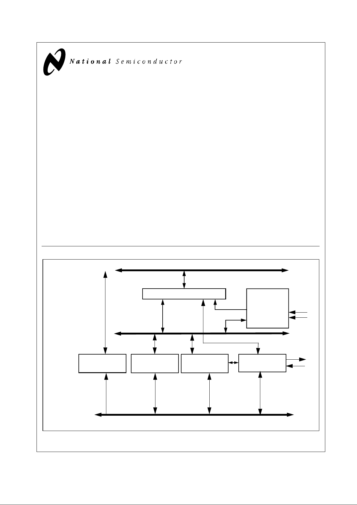
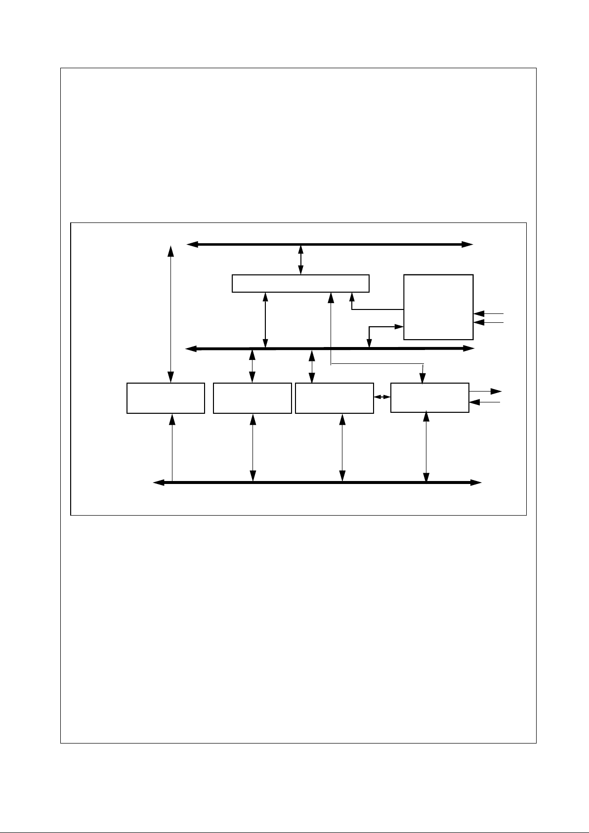
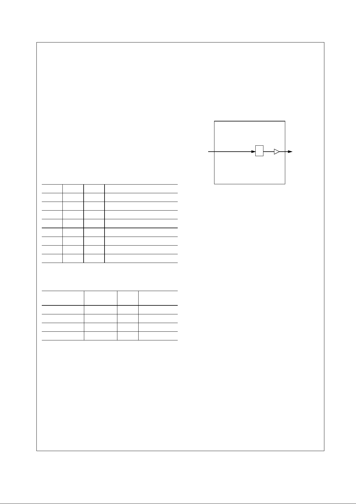
Block Diagram
X-Bus
ISA Bus
PCI Bus
PCI to X-Bus / X-Bus to PCI Bridge
PCI Configuration
Registers
X-Bus Arbiter
PC87200 Support
Serial IRQ Slave
mode interface logic
Serialized IRQ
Interface
PC/PCI DMA
Interface
ISA bus Target
Interface
ISA bus Master
Interface
PCPCIREQ#
PCPCIGNT#
Decoding logic
BPD#
PROHIBIT
TRI-STATE® is a registered trademark of National Semiconductor Corporation.
Page 2

2 www.national.com
Table of Contents
1.0 General Description . . . . . . . . . . . . . . . . . . . . . . . . . . . .1
2.0 Features . . . . . . . . . . . . . . . . . . . . . . . . . . . . . . . . . . . . . .1
2.1 General . . . . . . . . . . . . . . . . . . . . . . . . . . . . . . . . .1
2.2 PCI-to-ISA Bridge . . . . . . . . . . . . . . . . . . . . . . . . . 1
2.3 "PROHIBIT" functional support . . . . . . . . . . . . . . . 1
3.0 Device Overview . . . . . . . . . . . . . . . . . . . . . . . . . . . . . . .3
3.1 PCI Bus Interface . . . . . . . . . . . . . . . . . . . . . . . . . .3
3.2 ISA Bus Interface . . . . . . . . . . . . . . . . . . . . . . . . . . 3
3.3 Serialized IRQ support . . . . . . . . . . . . . . . . . . . . . .3
3.4 PROHIBIT signal support . . . . . . . . . . . . . . . . . . .5
3.5 PC/PCI DMA Interface Support . . . . . . . . . . . . . . . 5
4.0 Device Pinout . . . . . . . . . . . . . . . . . . . . . . . . . . . . . . . . . 7
5.0 Pin Descriptions . . . . . . . . . . . . . . . . . . . . . . . . . . . . . . . 8
5.1 Signal Definitions . . . . . . . . . . . . . . . . . . . . . . . . . .8
5.2 Pin Assignments . . . . . . . . . . . . . . . . . . . . . . . . . .9
5.3 Signal Descriptions . . . . . . . . . . . . . . . . . . . . . . . .9
6.0 Configuration . . . . . . . . . . . . . . . . . . . . . . . . . . . . . . . .15
7.0 Register Descriptions . . . . . . . . . . . . . . . . . . . . . . . . .16
7.1 Register Summary . . . . . . . . . . . . . . . . . . . . . . . .16
7.2 Chipset Register Space . . . . . . . . . . . . . . . . . . . .17
8.0 Electrical Characteristics . . . . . . . . . . . . . . . . . . . . . . .22
8.1 Electrical Specifications . . . . . . . . . . . . . . . . . . . .22
8.2 PC87200Test Modes . . . . . . . . . . . . . . . . . . . . . .22
8.3 Electrical Connections . . . . . . . . . . . . . . . . . . . . . 29
8.4 Absolute Maximum Ratings . . . . . . . . . . . . . . . . .29
8.5 Recommended Operating Conditions . . . . . . . . .29
8.6 DC Characteristics . . . . . . . . . . . . . . . . . . . . . . .30
8.7 AC Characteristics . . . . . . . . . . . . . . . . . . . . . . . .31
9.0 Physical Dimensions . . . . . . . . . . . . . . . . . . . . . . . . . . 33
Page 3
3 www.national.com
3.0 Device Overview
The PC87200 can be described as providing the functional
blocks shown in Figure 1.
— PCI bus master/slave interface
— ISA bus master/slave interface
— Serial IRQ slave mode interface
— PROHIBIT signal support
— PC/PCI DMA interface
3.1 PCI Bus Interface
The PC87200 provides a PCI bus interface that is both a
slave for PCI cycles initiated by the CPU or other PCI mas-
ter devices, and a PC/PCI DMA master for DMA transfer
cycles. The PC87200 supports positive decode for the
BIOS ROM in the special test mode and implements subtractive decode for unclaimed PCI accesses when the
PROHIBIT signal is low. The PC87200 also generates
address and data parity and performs parity checking.
Configuration registers are accessed through the PCI interface using the PCI Bus Type 1 configuration mechanism as
described in the PCI 2.1 Specification.
3.2 ISA Bus Interface
The PC87200 provides an ISA bus interface for subtractive-decoded memory and I/O cycles on PCI. The
PC87200 is the default subtractive decoding agent and will
forward all unclaimed memory and I/O cycles to the ISA
interface; however, the PC87200 may be configured to
ignore either I/O, memory or all unclaimed cycles (subtractive decode disabled) by asserting the PROHIBIT signal.
ISA master cycles will only be passed to the PCI bus if they
access memory. I/O accesses are left to complete on the
ISA bus.
ISA master cycles that access memory on ISA bus are not
supported by the PC87200.
3.3 Serialized IRQ support
The PC87200’s Serial Interrupt interface uses a serial
interrupt bus to transmit ISA Bus legacy interrupt requests.
The bus is a one pin bus(SERIRQ) and uses the PCI clock
as its timing reference. The serial interrupt bus is a multidrop bus that is shared by all PCI devices that have legacy
interrupts. The serial interrupt logic conforms to the serial-
ized IRQ defined in the Serialized IRQ on the “PCI way” Version 6.0 specification. Programming of the serial interrupt controller when the controller is currently running can
produce unexpected results.
X-Bus
ISA Bus
PCI Bus
PCI to X-Bus / X-Bus to PCI Bridge
PCI Configuration
Registers
X-Bus Arbiter
PC87200 Support
Serial IRQ Slave
mode interface logic
Serialized IRQ
Interface
PC/PCI DMA
Interface
ISA bus Target
Interface
ISA bus Master
Interface
PCPCIREQ#
PCPCIGNT#
Decoding logic
BPD#
PROHIBIT
Internal Block Diagram
Page 4
3.0 Device Overview (Continued)
4 www.national.com
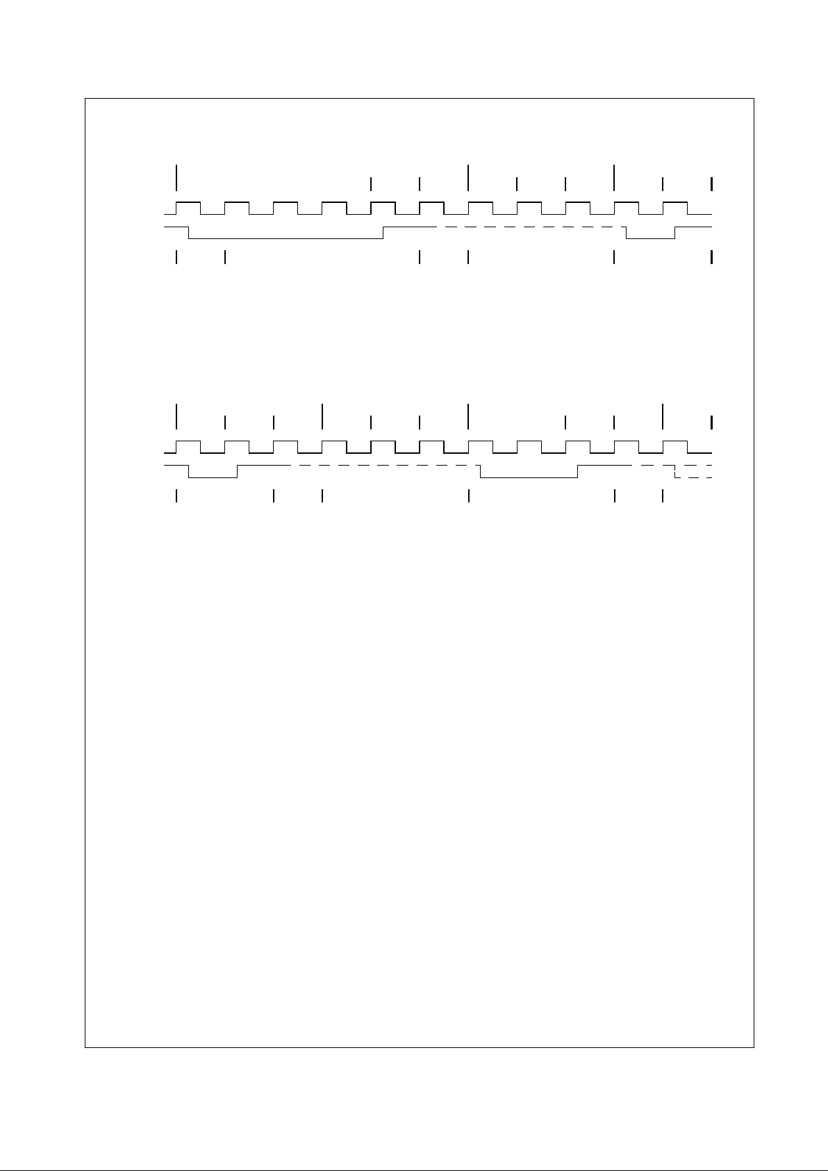
Timing of the serialized IRQ is illustrated as follows.
3.3.1 Serial Interrupts (Slave Mode)
There are two types of Serial Interrupt transfer modes; the
following describes the operation of the PC87200’s Serial
Interrupt Interface as a Slave:
1. Quiet Mode: Any Serial Interrupt device may initiate a
Start Cycle, while theSerial Interruptinterface isIdle, by
driving SERIRQ low for one PCI clock period. After driving lowfor one clock the device should immediately TRI-
STATE
®
SERIRQ, without ever driving this signal high.
A Start Cycle may not be initiated in the middleof an active Serial Interrupt transfer.Between Stopand Start Cycles the SERIRQsignal willbe pulled highand theSerial
Interrupt interface will be Idle.
When the PC87200 Serial Interrupt interface must initiate a Start Cycle in order to transfer any pending interrupt request to the Master. The only exception to this
requirementis whenaSerial Interrupttransfer sequence
is already in progressand the PC87200 can transferthe
request during this present Serial Interrupt transfer sequence,then the SerialInterrupt device isnotrequired to
generate another Start Cycle.
2. Continuous Mode: The PC87200 tracks both the Start
and Stop Frames and is responsible for inserting its interrupt requests on the appropriate IRQ frames.
3.3.2 IRQ Sampling Periods
Once a Start Cycle has been initiated all Serial Interrupt
devices watch for the rising edge of the Start Pulse and
start counting IRQ Sample periods from that point. Each
IRQ Sample Period is three clocks long, with the first clock
being the Sampled phase, the second clock being the
Recovery phase, and the third clock being the Turn-around
phase. During the Sample phase the Serial Interrupt
device drives SERIRQ low if its associated IRQ signal/data
is presently low. If its IRQ signal/data is high the Serial
Interrupt device must TRI-STATE SERIRQ. During the
Recovery phase, the Serial Interrupt device that drove
SERIRQ low (if any Serial Interface device does) is
required to drive back high. During the Turn-around phase
all Serial Interface devices will TRI-STATE SERIRQ. All
Serial Interface devices will drive SERIRQ low at the
appropriate sample point regardless of which device initiated the sample activity, if its associated IRQ signal/data is
low.
Slave
The PC87200 will support the interrupt request frames
listed in the following table.
The Generation clock for each IRQ follows the low to high
edge of the Start Pulse by the number of PCI Clocks listed
in Table 1.
Note: : The number of clocks equals: (3 x (IRQ number + 1)) - 1
3.3.3 Stop Cycle Control
The PC87200 will monitor SERIRQ for a Stop Cycle, so
that it may initiate a Start Cycle for a pending transition in
any of its IRQs (Quiet Mode). For Continuous Mode, the
PC87200 will not initiate any Start Cycle, but will track the
Start and Stop Cycles and insert its IRQs appropriately.
PCI CLK
SERIRQ
START R T S R T S R
START CYCLE
START
Driving
Source
Slave (Q)
Master (C)
Master NONE NONE IRQ1 Source
IRQ0 IRQ1
R = Recovery; T= Turn-around; S = Sample
Start Cycle Timing
PCI CLK
SERIRQ
RTSRTTR
STOP CYCLE
Driving
Source
IRQ15 Source MasterNONE NONE NONE
IRQ15
R = Recovery; T= Turn-around; S = Sample
S
STOP
(NOTE 1)
START
IOCHK#
NOTE 1: The Stop pulse is 2 clocks wide for Quiet mode, 3 clocks wide for Continuous mode
Stop Cycle Timing
Page 5
3.0 Device Overview (Continued)
5 www.national.com
3.4 PROHIBIT signal support
The chipset will use this signal to claim the BIOS first and
then deassert the "PROHIBIT" signal to configure the PCI
to ISA bridge to continue the boot sequence.
Special test mode support is provided by means of the
BPD# pin. When this test mode is active, the PC87200 will
enable positive memory decode during boot up to enable
the host to look for boot ROM on ISA card.
PROHIBIT will be a don’t care in this test mode at boot up
for the ROM BIOS range, but should function normally after
booting
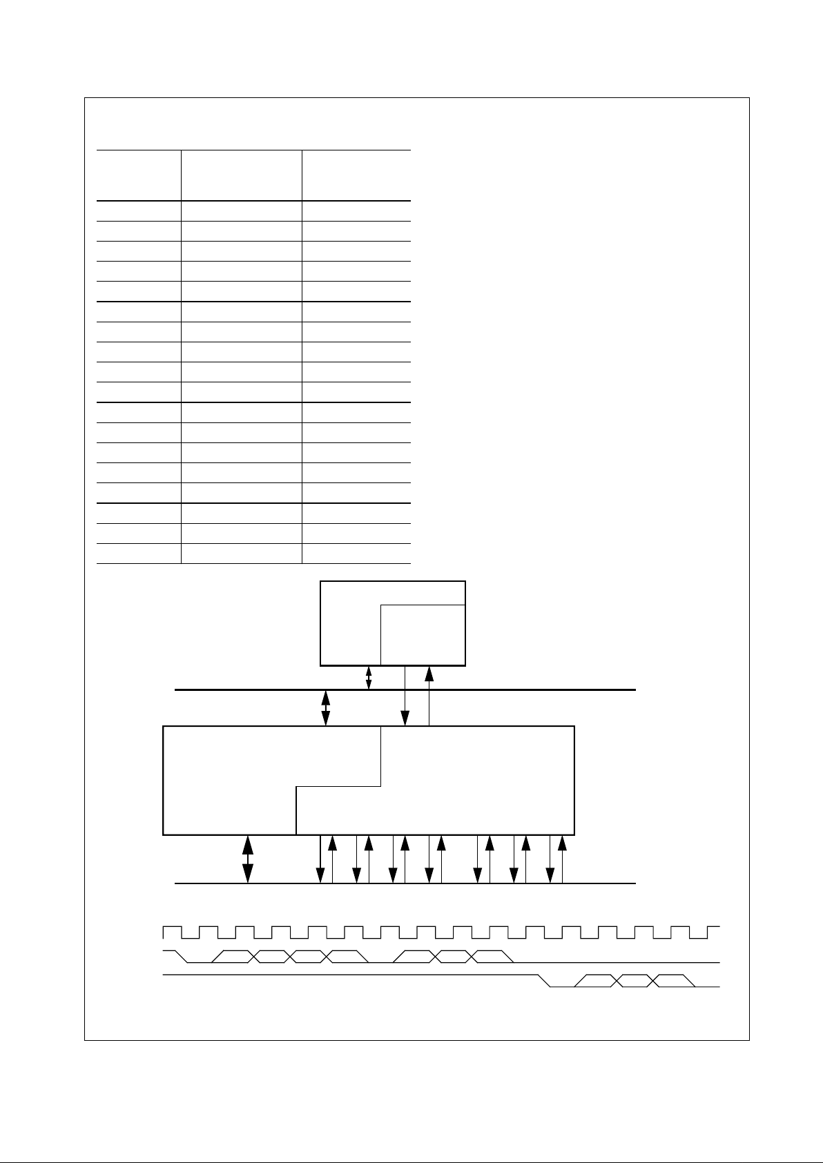
3.5 PC/PCI DMA Interface Support
The PC87200 operatesas a PC/PCI DMA Secondary Arbitration Bridge. The PC87200 can passall seven legacy ISA
bus DMA channel requests to the PC/PCI DMA Primary
Bus Arbiter using the channel passing protocol defined in
the Moble PC/PCI DMA Arbitration and Protocol Specification (Revision 2.2). Figure 1 shows the topology of the
PC87200 PC/PCI DMA requests and grants:
The PC87200 converts the seven legacy ISA bus DMA
requests (DREQ0, 1, 2, 3, 5, 6 and 7) into a serial PC/PCI
DMA compliant REQ# sequence and converts the corresponding PC/PCI DMA GNT# sequence into the appropriate DMAacknowledge (DACK0-3, 5-7#). ThisPC/PCI DMA
expansion Channel Passing Protocol is illustrated
Figure 2.
Table 1. SERIRQ Slave Generation Periods
SERIRQ
Period
Signal Generated
# of clocks past
Start
1 Reserved. 2
2 Reserved. 5
3 Reserved. 8
4 IRQ3 11
5 IRQ4 14
6 IRQ5 17
7 IRQ6 20
8 IRQ7 23
9 Reserved. 26
10 IRQ9 29
11 IRQ10 32
12 IRQ11 35
13 IRQ12 38
14 Reserved. 41
15 IRQ14 44
16 IRQ15 47
17 IOCHK# 50
21:18 Reserved. 62,59,56, 53
Figure 1. PC87200 PC/PCI DMA Topology
Figure 2. Channel Passing Protocol
PC/PCI DMA
Primary Bus
Arbiter
PCI Bus
PCPCIREQ#
PCPCIGNT#
PC87200
DACK0#
DREQ0
DACK1#
DREQ1
DACK2#
DREQ2
DACK3#
DREQ3
DACK5#
DREQ5
DACK6#
DREQ6
DACK7#
DREQ7
PC/PCI DMA Interface Support
ISA Bus
start
CH0
CH1
CH2 CH3 CH4 CH5 CH6
CH7
start
bit 0 bit 1 bit 2
PCICLK
PCPCIREQ#
PCPCIGNT#
Page 6
3.0 Device Overview (Continued)
6 www.national.com
When a legacy ISA bus DMA request is asserted, the
PC87200 will transmit that request to the PC/PCI Primary
Bus Arbiter by encoding it and driving it out the PC87200’s
PCPCIREQ# according to the above; first PCPCIREQ# will
be driven low for one PCICLK period to indicate that the
serial encoded request transfer is starting. Then the
PC87200 willdrive each ofthe next eight bits with the value
of its corresponding DREQ. (NOTE: Channel 4 will always
be driven low.) At the end of the request sequence, the
PC87200 will continue to drive its PCPCIREQ# signal
active, indicating that the request is still being maintained.
In response to the request sequence, the PC/PCI Primary
Bus Arbiter will respond with a PC/PCI DMA encoded grant
transfer when it is granting the PCI bus for a PC/PCI DMA
transfer cycle. The PC/PCI encoded grant transfer will
begin when the PC/PCI Primary Bus Arbiter drives
PCPCIGNT# low for one PCICLK period to indicate the
start of the grant sequence; then the next three
PCPCIGNT# signal PCICLK periods will then contain the
encoded grant value, indicating which legacy ISA DMA
channel is being granted the PC Bus.
After receiving a valid grant from the PC/PCI DMA Arbiter,
the PC87200 will recognize the following I/O accesses as
DMA I/O Reads(Writes) from (to) the granted legacy ISA
DMA channel.
PCI bus address bit 2 (A2) indicates if the cycle is to be a
Terminal Count cycle or not.
For Normal DMA Cycles, PCI bus I/O Reads and Writes
will be translated to legacy ISA DMA Reads and Writes
respectively. For Verify DMA Cycles, only PCI bus I/O
Reads will be translated to legacy ISA DMA Verify cycles.
3.5.4 Clock Generation
The PC87200 generates the ISA clock using PCI clock signal (typically 33 MHz).
A PCICLK divisor (3,4) is programmable through PCI configuration register to generate the ISA clock signal. This
provides support for the generation of ISACLK frequencies
8.33 MHz and 11 MHz off of a 33MHz PCICLK.
Figure 3. showsa block diagramfor clock generation within
the PC87200.
bit 2 bit 1 bit 0 Channel Granted
0 0 0 DMA Channel 0 (DACK0#)
0 0 1 DMA Channel 0 (DACK1#)
0 1 0 DMA Channel 0 (DACK2#)
0 1 1 DMA Channel 0 (DACK3#)
1 0 0 RESERVED
1 0 1 DMA Channel 0 (DACK5#)
1 1 0 DMA Channel 0 (DACK6#)
1 1 1 DMA Channel 0 (DACK7#)
DMA Cycle
Type
DMA
I/O Address
TC (A2) PCI Cycle Type
Normal 0000_0000h 0 I/O Read/Write
Normal TC 0000_0004h 1 I/O Read/Write
Verify 0000_00C0h 0 I/O Read
Verify TC 0000_00C4h 1 I/O Read.
Figure 3. PC87200 Clock Generation
N
SYSCLKPCICLK
PC87200
Page 7
7 www.national.com
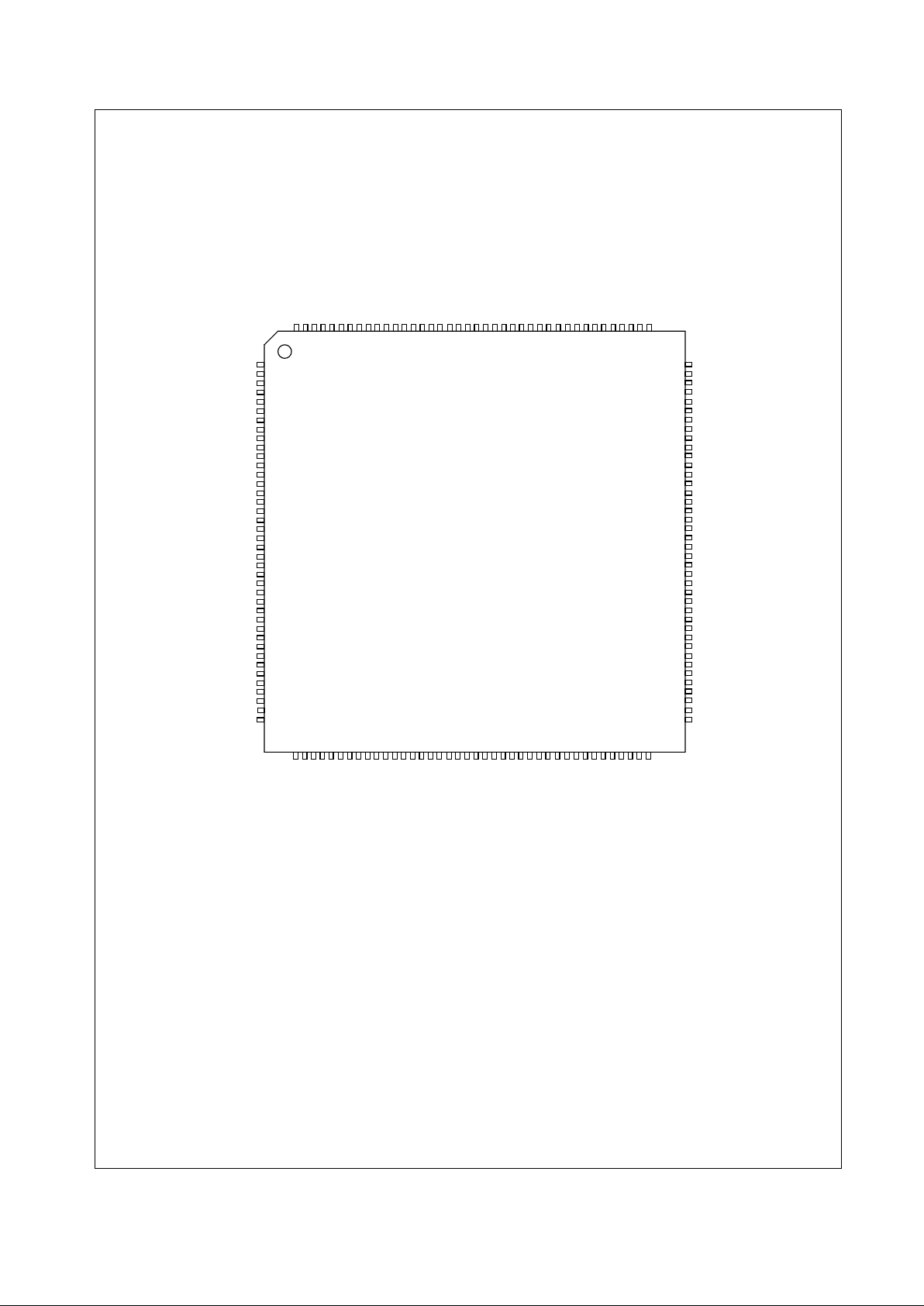
4.0 Device Pinout
AD31
1
2
3
4
5
6
7
8
9
10
11
12
13
14
15
16
17
18
19
20
21
22
23
24
25
26
27
28
29
30
31
32
33
34
35
36
37
38
39
40
414243444546474849505152535455565758596061626364656667686970717273747576777879
80
120
119
118
117
116
115
114
113
112
111
110
109
108
107
106
105
104
103
102
101
100
99
98
97
96
95
94
93
92
91
90
89
88
87
86
85
84
83
82
81
160
159
158
157
156
155
154
153
152
151
150
149
148
147
146
145
144
143
142
141
140
139
138
137
136
135
134
133
132
131
130
129
128
127
126
125
124
123
122
121
Vdd
Vss
SA18
SA19
DACK2#
DREQ2
SYSCLK
SD7
SD6
SD5
SD4
IOCHK#
SD3
SD2
SD1
SD0
Vdd
Vss
IOCHRDY
SMEMR#
AEN
SMEMW#
IOR#
IOW#
MEMCS16#
IOCS16#
SA20
SA21
SA22
SA23
IRQ10
IRQ11
IRQ9
IRQ12
IRQ15
IRQ14
Vdd
Vss
DACK0#
DREQ0
MEMR#
MEMW#
DACK5#
DREQ5
SD8
SD9
SD10
SD11
DACK6#
DREQ6
SD12
SD13
SD14
SD15
DACK7#
DREQ7
Vdd
Vss
MASTER#
SBHE#
TC
BPD#
AD30
AD29
AD28
AD27
AD26
Vdd
Vss
C/BE3#
IDSEL
AD23
AD22
AD25
AD24
Vdd
Vss
AD0
AD1
AD2
AD3
AD4
AD5
Vss
Vdd
AD6
AD7
C/BE0#
AD8
AD9
AD10
Vss
Vdd
AD11
AD12
AD13
AD14
AD15
C/BE1#
Vss
Vdd
PAR
SERR#
STOP#
DEVSEL#
TRDY#
IRDY#
Vss
Vdd
FRAME#
C/BE2#
AD16
AD17
AD18
AD19
AD20
AD21
SA17
SA16
SA15
SA14
SA13
SA12
SA11
SA10
SA9
Vss
Vdd
SA8
SA7
SA6
SA5
SA4
SA3
SA2
SA1
SA0
Vss
Vdd
PROHIBIT
DREQ1
DACK1#
RSTDRV
DREQ3
DACK3#
IRQ7
IRQ6
IRQ5
IRQ4
IRQ3
SERIRQ
PCPCIGNT#
PCPCIREQ#
PCIRST#
PCICLK
Vss
Vdd
BALE
REFRESH#
Page 8
8 www.national.com
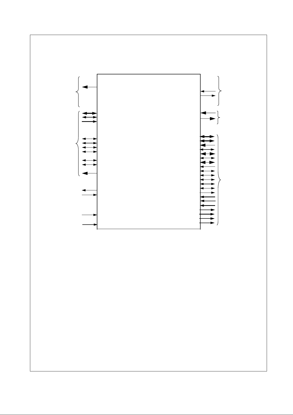
5.0 Pin Descriptions
5.1 Signal Definitions
This section defines the signals and describes the external interface of the PC87200. The following diagram shows the
pins organized by their functional groupings. Internal test and electrical pins are not shown.
AD[31:0]
C/BE[3:0]#
PAR
FRAME#
TRDY#
STOP#
DEVSEL#
SERR#
IDSEL
SERIRQ
PCI Bus
IRQ Interface
IRDY#
PCICLK
SYSCLK
Clocks
Reset
PCIRST#
PC87200
SA[23:0]
IOCHK#
SBHE#
BALE
IOCHRDY
REFRESH#
IOR#
IOW#
MEMCS16#
MEMR#
MEMW#
AEN
DREQ[7:5], [3:0]
DACK#[7:5], [3:0]
TC
IRQ[15:14], [12:9], [7:3]
ISA Bus
IOCS16#
SD[15:0]
SMEMW#
SMEMR#
Serialized
PROHIBIT
MASTER#
BPD#
RSTDRV
PC87200 Signal Groups
PCPCIGNT#
PCPCIREQ#
Enhanced Integrated PCI-to-ISA
Bridge
Page 9
9 www.national.com
5.0 Pin Descriptions (Continued)
5.2 Pin Assignments
The tables in this section use several common abbreviations. Table 2. lists the mnemonics and their meanings.
In the next section, description of each signal within its associated functional group is provided.
5.3 Signal Descriptions
5.3.1 Reset Signals
5.3.2 Clock Interface Signals
Table 2. Pin Type Definitions
Mnemonic Definition
I Standard input pin.
I/O Bidirectional pin.
O Totem-pole output.
OD Open-drain output structure that allows multiple devices to share the pin in a wired-OR configuration.
PU Pull-up resistor.
PD Pull-down resistor.
smt Schmitt Trigger.
s/t/s Sustained TRI-STATE, an active-low TRI-STATE signal owned and driven by one and only one agent at a
time. The agent that drives an s/t/s pin low must drive it high for at least one clock before letting it float. A
new agent cannot start drivingan s/t/ssignal anysooner thanone clockafter theprevious owner lets it float.
A pull-up resistor is required to sustain the inactive state until another agent drives itand must be provided
by the central resource.
t/s TRI-STATE signal.
VDD (PWR) Power pin.
VSS (GND) Ground pin.
# The"#" symbolat theend of asignal name indicatesthatthe active,orasserted stateoccurs whenthe signal
is at a lowvoltage level. When "#" is not presentafter thesignal name, the signal isasserted whenat a high
voltage level.
Signal Name Pin
No.
Type Description
PCIRST# 124 I PCI Reset
PCIRST# is the reset signal for the PCI bus.
RSTDRV 135 O Reset Drive
This signal is asserted to reset devices that reside on the ISA bus. It will be driven
by the inverse of the PCIRST# input signal.
Signal Name Pin No. Type Description
PCICLK 123 I PCI Clock
This clock runs at the PCI clock frequency and is used to drive most of the
PC87200 circuitry.
SYSCLK 8 O ISA Bus Clock
ISACLK is derived from PCICLK and is typically programmed for 8.33MHz.
F0 Index 50h[2:0]is usedto program the ISA clockdivisor. Thesebits determine
the divisor of the PCI clock used to generate the ISA bus clock. If F0 Index
50h[2:0] is set to:
010 = Divide by three (sysclk=11MHz)
011 = Divide by four (sysclk = 8.33MHz)
All other values are invalid and can produce unexpected results.
Page 10

10 www.national.com
5.0 Pin Descriptions (Continued)
5.3.3 PCI Interface Signals
Signal Name Pin No. Type Description
AD[31:0] 65,66,
67,68,
69,70,
73,74,
77,78,
81,82,
83,84,
85,86,
100,101,
102,103,
104,107,
108,109,
111,112,
115,116,
117,118,
119,120
I/O
t/s
PCI Address/Data
AD[31:0] is a physicaladdress duringthe firstclock ofa PCI transaction; it is the
data during subsequent clocks.
When the PC87200 is a PCI master, AD[31:0] are outputs during the address
and write data phases, and are inputs during the read data phase of a transaction.
When the PC87200 is a PCI slave, AD[31:0] are inputs during the address and
write data phases, and are outputs during the read data phase of a transaction.
C/BE[3:0]# 75,87,
99,110
I/O
t/s
PCI Bus Command and Byte Enables
During the address phaseof aPCI transaction, C/BE[3:0]# defines the bus com-
mand. During the data phase of a transaction, C/BE[3:0]# are the data byte enables.
C/BE[3:0]# are outputs whenthe PC87200is aPCI master and are inputs when
it is a PCI slave.
IDSEL 76 I Initialization Device Select
It is used as a chip select during configuration read and write transactions.
FRAME# 88 I/O
t/s
PCI Cycle Frame
FRAME# is assertedto indicatethe startand durationof a transaction. It isdeas-
serted on the final data phase.
FRAME# is an input when the PC87200 is a PCI slave.
IRDY# 91 I/O
t/s
PCI Initiator Ready
IRDY#is drivenbythe masterto indicatevalid data ona write transaction,or that
it is ready to receive data on a read transaction.
When the PC87200 is a PCI slave, IRDY# is an input that can delay the begin-
ning of a write transaction or the completion of a read transaction.
Wait cycles are inserted until both IRDY# and TRDY# are asserted together.
TRDY# 92 I/O
t/s
PCI Target Ready
TRDY# is asserted by a PCIslave to indicate it is ready tocomplete the current
data transfer.
TRDY# is an input that indicates a PCI slave has driven valid data on a read or
a PCI slave is ready to accept data from the PC87200 on a write.
TRDY# is an output that indicates the PC87200 has placed valid data on
AD[31:0] during a read or is ready to accept the data from a PCI master on a
write.
Wait cycles are inserted until both IRDY# and TRDY# are asserted together.
STOP# 94 I/O
t/s
PCI Stop
As an input, STOP# indicates that a PCI slave wants to terminate the current
transfer. The transfer will be aborted, retried, or disconnected.
As anoutput, STOP# is asserted withTRDY# to indicate a targetdisconnect, or
without TRDY# to indicate a target retry.
Page 11

5.0 Pin Descriptions (Continued)
11 www.national.com
DEVSEL# 93 I/O
t/s
PCI Device Select
DEVSEL#is assertedbya PCIslave, to indicateto a PCImaster and subtractive
decoder that it is the target of the current transaction.
As an input, DEVSEL# indicates a PCI slave has responded to the current ad-
dress.
As an output, DEVSEL# is asserted one cycle after the assertion of FRAME#
and remains asserted to the end of a transaction as the result of a positive decode. DEVSEL# is asserted four cycles after the assertion of FRAME# if the
PC87200 is selected as the result of a subtractive decode. The subtractive decode sample point can be configured in F0 Index 41h[2:1]. These cycles are
passed to the ISA bus.
PAR 96 I/O
t/s
PCI Parity
PAR is the parity signal driven to maintain even parity across AD[31:0] and
C/BE[3:0]#.
The PC87200 drivesPAR oneclock afterthe addressphase and one clock after
each completeddata phase ofwrite transactions asa PCI master.It also drives
PAR one clock after each completed data phase of read transactions as a PCI
slave.
SERR# 95 OODPCI System Error
SERR# is pulsed by a PCI device to indicate an address parity error.
Signal Name Pin No. Type Description
Page 12

5.0 Pin Descriptions (Continued)
12 www.national.com
5.3.4 ISA Bus Interface Signals
Signal Name Pin No. Type Description
MASTER# 61 I ISA Master Mode: Master
TheMASTER# inputassertedindicates anISAbus masterisdriving theISAbus
and that it may access any device on the system board.
SA[23:0] 33,32,
31,30,
4,3,160,
159,158,
157,156,
155,154,
153,152,
149,148,
147,146,
145,144,
143,142,
141
I/O System Address Bus
This bus carries the addresses for all ISA cycles.
SD[15:0] 56,55,
54,53,
50,49,
48,47,
9,10,
11,12,
15,16,
17,18
I/O System Data Bus
This bus carries the data for all ISA cycles.
SMEMW# 24 O System Memory Write
SMEMW# is output on this pin. SMEMW# is asserted for any memory write accesses below 1MB. It enables 8-bit memory slaves to decode the memory address on SA[19:0].
SMEMR# 22 O System Memory Read
SMEMR# isoutput onthis pin. SMEMR# is assertedfor memory read accesses
below 1MB. It enables 8-bit memory slaves to decode the memory address on
SA[19:0].
SBHE# 62 I/O System Bus High Enable
The PC87200 or ISA master asserts SBHE# to indicate that SD[15:8] will be
used to transfer a byte at an odd address.
SBHE# is an output during non-ISA master DMA operations. It is driven as the
inversion of AD0 during 8-bit DMA cycles. It is forced low for all 16-bit DMA cycles.
SBHE# is an input during ISA master operations.
BALE 27 I/O Buffered Address Latch Enable/Special Test mode
BALE indicates when SA[23:0] and SBHE# are valid and may be latched. This
pin will be used as strap for special test mode with the PROHIBIT signal by
checking its input level during reset.
IOCHRDY 21 I/OODI/O Channel Ready
IOCHRDYdeasserted indicates thatan ISAslave requiresadditionalwait states.
When the PC87200 is an ISA slave, IOCHRDYis anoutput indicatingadditional
wait states are required.
REFRESH# 14 I/OODRefresh Cycle indicator
The PC87200 supports the standard ISA refresh function. When the ISA bus is
not in use by the ISA bus controller, the DMA controller, or an ISA bus master,
the refresh control logic will generate an ISA refresh cycle. The 87200 also supports refresh requests initiated by ISA masters.
Page 13

5.0 Pin Descriptions (Continued)
13 www.national.com
5.3.5 Miscellaneous Signals (Continued)
IOCS16# 29 I I/O Chip Select 16
IOCS16# is asserted by 16-bit ISA I/O devices based on an asynchronous decodeof SA[15:0]to indicatethat SD[15:0] maybe used totransferdata (8-bitISA
I/O devices use SD[7:0]).
IOR# 25 I/O I/O Read
IOR# is asserted to request an ISA I/O slave to drive data onto the data bus.
IOW# 26 I/O I/O Write
IOW# is asserted to request an ISA I/O slave to accept data from the data bus.
MEMCS16# 28 I/OODMemory Chip Select 16
MEMCS# is asserted by 16-bit ISAmemory devicesbased onan asynchronous
decode of SA[23:17] to indicate that SD[15:0] may be used to transfer data (8bit ISA memory devices use SD[7:0]).
MEMR# 43 I/O Memory Read
MEMR# is asserted for all memory read accesses (including those above 1MB).
It enables 16-bit memory slaves to decode the memory address on SA[23:0].
MEMW# 44 I/O Memory Write
MEMW#is asserted forall memory writeaccesses (includingthose above 1MB).
It enables 16-bit memory slaves to decode the memory address on SA[23:0].
AEN 23 O Address Enable
AEN asserted indicates to ISA memory devices that a valid address for a DMA
transfer is present on SA[23:0], and for I/O devices to ignore this address and
any data on the ISA bus.
IRQ[15:14], [12:9],
[7:3]
37,38,
36,35,
34,5,
132,131,
130,129,
128
I ISA Bus Interrupt Request
IRQ inputs are interrupts that indicateISA devicesor otherdevices requestinga
CPU interrupt service.
DREQ[7:5],
DREQ[3:0]
58 52,
46,134,
7,137,42
I DMA Request - Channels [7:5], [3:0]
DREQ inputsare asserted byISA DMA devicesto request aDMA transfer. The
request must remain asserted until the corresponding DACK# is asserted.
DACK[7:5]#,
DACK[3:0]#
57,51,
45,133,
6,136,41
O DMA Acknowledge- Channels [7:5], [3:0]
DACK# outputs are asserted to indicate when a DREQ is granted and the start
of a DMA cycle.
TC 63 O Terminal Count
TC signals the final data transfer of a DMA transfer.
IOCHK# 13 I I/O channel check
Asserted by an ISA device indicating an error condition.
Signal Name Pin No. Type Description
Signal Name Pin No. Type Description
SERIRQ 127 I/O
s/t/s
Serial IRQ
This is a one pin bus that conveys interrupt source information to the chipset.
PROHIBIT 138 I PROHIBIT
Anactive highsignal from thechipset indicating thatthe PC87200shouldnot act
as the subtractive decode agent on the PCI bus.
BPD# 64 I BIOS Positive Decode (active low)
When this pin is asserted low after BALE is detected high after reset, the PROHIBIT signal will be a don’t care. The BIOS memory range will be positively decoded and claimed as such. All other cycles are still subtractively decoded.
Page 14

5.0 Pin Descriptions (Continued)
14 www.national.com
5.3.6 PC/PCI signals
5.3.7 Power, Ground, and Reserved Terminals
PCPCIREQ# 125 O PC/PCI Bus Request
The PC87200 asserts PCPCIREQ# using the PC/PCI DMA request protocol in
response to a DMA request or ISA master requestto gain ownership of the PCI
bus.The PCPCIREQ#and PCPCIGNT# signalsare used toarbitrate for thePCI
bus.
PCPCIGNT# 126 I PC/PCI Bus Grant
PCPCIGNT# is assertedusing thePC/PCI DMA grantprotocol byan arbiterthat
indicates to the PC87200 that access to the PCI bus has been granted.
Signal Name Pin No. Type Description
VDD 1,19,39,
59,71,
79,89,
97,105,
113,121,
139,150
PWR 3.3V (nominal) Power Connection
VSS 2,20,40,
60,72,
80,90,
98,106,
114,122,
140,151
GND Ground Connection
Page 15

15 www.national.com
6.0 Configuration
a. Connect the NOGO signal of the south bridge to Prohibit
pin of PC87200, SERIRQ to SERIRQ, REQ[A] to
PCPCIREQ#, GNT[A] to PCPCIGNT# (other PC/PCI REQ,
GNT pair may also be used). If BPD# is not being used, it
should be pulled high.
b. On power-up reset (i.e., cold boot), the NOGO signal is
high on reset and therefore disables the subtractive decoding capability of PC87200. The rationale for doing this is as
follows: on the PCI bus, only one subtractive decoding
agent can exist. Since the south bridge will normally power
up as the subtractive decoding agent, the PC87200 must
be “prohibited” from doing so. Any other GPO pin which is
high on reset can also be used.
c. After PCI bus enumeration, when the device ID and vendor ID of PC87200 is found, do the following:
d. Enable serial IRQ in continuous mode, 21 frames and 4
clock start frame by setting register 64h of south bridge to
d0h. (In the old south bridge, the serial IRQ pin is multiplexed with a GPIO and need to be selected as serial IRQ.
In the latest industry standard south bridge, however, the
serial IRQ is a dedicated pin and does not require initialization.)
e. Enable PC/PCI DMA by setting the PC/PCI request and
grant pins to PC/PCI DMA mode, instead of using them as
GPIOs. Any PC/PCI request and grant pair can be used,
but on the south bridge, GNT[B] is multiplexed with GNT[5],
so PC/PCI request and grant pair A is more preferable to
use.
Set all channels of DMA to PC/PCI DMA except for channels 4 & 2 (channel 4 is for cascading the DMAC and channel 2 is for FDC). The value to be put in register 91:90 is
5475 for the latest south bridge and 5455 for older south
bridges. The difference is due to the use of “11” for LPC
DMA, and the value of 00 (ISA DMA) being put into
reserved instead.
f. Enable positive decode for the devices under the new
south bridge: program the value of 3C0F into reg. E7:E6
will enable positive decode for most devices except sound
and gameport. Changing it to enable/disable other devices
will be straightforward for the new south bridge. (For old
south bridges, it will be harder, and requires one to find all
the bits to set/reset. )
g. Enable the new south bridge to do positive decode by
setting bit 1 of reg. B0h to 1.
h. Set the NOGO signal to low.
i.
Program register 42h of PC87200 to 20h. This is a
required initialization step.
j. Program a value of 03 into register D3h of device 1Fh in
function 0 of the new south bridge. This will prevent the
PC87200 from responding to configuration accesses afterwards. The rationale for doing this is to prevent Windows
from detecting two ISA bridges, the other one being the
PCI-to-LPC bridge, and thus creating a conflict. NOTE that
you must connect AD22 to IDSEL of PC87200 for this to
work.
After this, proceed in normal BIOS flow. Note that step d to
j must be performed before ISA bus enumeration, and
therefore before ISA plug and play initialization and option
ROM checking. This is needed for plug and play cards and
cards with option ROM (e.g.,VGA cards, SCSI cards) to
work properly.
Page 16

16 www.national.com
7.0 Register Descriptions
The 87200 is a single function device. Its register space is
called the Bridge Configuration Registers Space (F0)
which is accessed through the PCI interface using the PCI
Type One Configuration Mechanism.
The PCI header is a 256-byte region used for configuring a
PCI device or function. The first 64 bytes are the same for
all PCIdevices and are predefined bythe PCI specification.
These registers are used to configure the PCI for the
device. The rest of the 256-byte region is used to configure
the device or function itself.
The remaining subsections of this chapter is as follows:
— A briefdiscussion onhow to accessthe registers located
in the PCI Configuration Space.
— Register summary.
— Detailed bit formats of all registers.
7.1 Register Summary
The tables in this subsection summarize all the registers of
the PC87200. Included in the tables are the register’s reset
values.
Table 3. Function 0: Bridge Configuration Registers Summary
F0 Index Width (Bits) Type Name Reset Value
00h-01h 16 RO Vendor Identification Register 100Bh
02h-03h 16 RO Device Identification Register 0021h
04h-05h 16 R/W PCI Command Register 0107h
06h-07h 16 R/W PCI Status Register 0280h
08h 8 RO Device Revision ID Register 00h
09h-0Bh 24 RO PCI Class Code Register 060100h
0Ch 8 R/W PCI Cache Line Size Register 00h
0Dh 8 R/W PCI Latency Timer Register 00h
0Eh 8 RO PCI Header Type Register 00h
0Fh 8 RO PCI BIST Register 00h
10h-3Fh -- -- Reserved 00h
40h 8 R/W PCI Function Control Register 1 79h
41h 8 R/W PCI Function Control Register 2 10h
42h 8 R/W PCI Function Control Register 3 28h
43h 8 R/W PCI Function Control Register 4 46h
44h 8 R/W Reset Control Register 00h
45h-4Fh -- -- Internal use, do not overwrite -50h 8 R/W ISA CLK Divider 43h
51h 8 R/W ISA I/O Recovery Control Register 43h
52h 8 R/W ROM/AT Logic Control Register 04h
53h-5Ah -- -- Internal use, do not overwrite -5Bh 8 R/W Decode Control Register 2 00h
5Ch-FFh -- -- Internal use, do not overwrite --
Page 17

7.0 Register Descriptions (Continued)
17 www.national.com
7.2 Chipset Register Space
The Chipset Register Space of the PC87200 is comprised
of one function with PCI header registers. There is no
memory or I/O mapped register.
7.2.1 Bridge Configuration Registers - Function 0
The register space designated as Function 0 (F0) contains
registers used to configure features and functionality
unique to the PC87200. All registers in Function 0 are
directly accessed (i.e., there are no memory or I/O mapped
registers in F0). Table 4 gives the bit formats for these registers.
IMPORTANT: Register bits marked internal use should
not be overwritten, else error will occur
.
Table 4. Bridge Configuration Registers
Bit Description
Index 00h-01h Vendor Identification Register (RO) ResetValue =100Bh
Index 02h-03h Device Identification Register (RO) ResetValue=0021h
Index 04h-05h PCI Command Register (R/W) ResetValue =0107h
15:10 Reserved — Set to 0.
9 Fast Back-to-Back Enable (Read Only) — This function is not supported when PC87200 is a master. It is al-
ways disabled (must always be set to 0).
8 SERR# — Allow SERR# assertion on detection of special errors: 0 = Disable; 1 = Enable.
7 Wait Cycle Control (Read Only) — This function is not supported in PC87200. It is always disabled (bit is set
to 0).
6 Parity Error — Allow PC87200 to check for parity errors on PCI cycles for which it is a target, and to assert
PERR# when a parity error is detected: 0 = Disable; 1 = Enable.
5 VGA Palette Snoop Enable (Read Only) — This function is not supported in PC87200. It is always disabled
(bit is set to 0).
4
Memory Write and Invalidate —
Allow PC87200 to do memory write and invalidate cycles, if the PCI
cache line register is set to 16 bytes (04h). 0=Disable, 1=Enable.
3 Special Cycles — This function is not supported. It must always be set to 0.
2 Bus Master — Allow PC87200 bus mastering capabilities: 0 = Disable; 1 = Enable. Set this bit to 1.
1 Memory Space — Allow PC87200 to respond to memory cycles from the PCI bus: 0 = Disable; 1 = Enable.
PC87200 will only respond to memory cycles destined for the ISA bus as none of its internal functions are
memory-mapped.
0 I/O Space — Allow PC87200 to respond to I/O cycles from the PCI bus: 0 = Disable; 1 = Enable.
Index 06h-07h PCI Status Register (R/W) Reset Value = 0280h
15 Detected Parity Error — This bit is set whenever a parity error is detected. Write 1 to clear.
14 Signaled System Error — This bit is set whenever PC87200 asserts SERR# active. Write 1 to clear.
13 Received Master Abort — This bit is set whenever a master abort cycle occurs. A master abort will occur
when a PCI cycle is not claimed, except for special cycles. Write 1 to clear. Register is cleared after RMA is
read.
12 ReceivedTarget Abort — This bitis set whenever a targetabort is received while thePC87200 is the master
for the PCI cycle. Write 1 to clear.
11 Signaled Target Abort — This bit is set whenever the PC87200 signals a target abort. This occurs when an
address parity erroroccurs foran address thathits inthe active addressdecode spaceof the PC87200.Write
1 to clear.
10:9 DEVSEL# Timing — These bits are always 01, as the PC87200 will always respond to cycles for which it is
an active target with medium DEVSEL# timing.
00 = Fast
01 = Medium
10 = Slow
11 = Reserved
Page 18

18 www.national.com
7.0 Register Descriptions (Continued)
8 Data Parity Detected —This bit is set when:
1) The PC87200 asserted PERR# or observed PERR# asserted.
2) PC87200 is the master for the cycle in which the PERR# occurred, and PE is set (F0 Index 04h[6] = 1).
Write 1 to clear.
7 Fast Back-to-Back Capable — As a target, PC87200 is capable ofaccepting fast back-to-back transactions:
0 = Disable; 1 = Enable. This bit is always set to 1.
6:0 Reserved — Set to 0.
Index 08h Device Revision ID Register (RO) Reset Value = 00h
Index 09h-0Bh PCI Class Code Register (RO) Reset Value = 060100h
Index 0Ch PCI Cache Line Size Register (R/W) Reset Value = 00h
7:0 PCI Cache Line Size Register — reserved.
Index 0Dh PCI Latency Timer Register (R/W) Reset Value = 00h
7:4 Reserved — Set to 0.
3:0 PCI Latency Timer Value— The PCI Latency TimerRegister prevents system lockup whena slave does not
respond to a cycle that the PC87200 masters. If the value is set to 00h (default), the timer is disabled. If the
timer is written with any other value, bits [3:0] become the four most significant bytes in a timer that counts
PCI clocks for slave response. Thetimer isreset oneach validdata transfer.If thecounter expiresbefore the
next assertion of TRDY# is received, the PC87200 stops the transaction with a master abort and asserts
SERR#, if enabled to do so.
Index 0Eh PCI Header Type (RO) ResetValue=00h
7:0 PCI Header Type Register — This.register defines theformat of thisheader. This headeris of typeformat 0.
Additionally, bit 7 defines whether this PCI device is a multifunction device (bit 7 = 1) or not (bit 7 = 0).
Index 0Fh PCI BIST Register (RO) Reset Value = 00h
7:0 Reserved. Set to 0.
Index 10h-3Fh Reserved Reset Value = 00h
Index 40h PCI Function Control Register 1 (R/W) ResetValue =79h
7 Internal use, do not overwrite.
6 Single Write Mode — PC87200 accepts only single cycle write transfers as a slave on the PCI bus and per-
forms a target disconnect with the first data transferred: 0 = Disable(accepts burst write cycles); 1 = Enable.
5 Single Read Mode — PC87200 accepts only single cycle read transfers as a slave on the PCI bus and per-
forms a target disconnect with the first data transferred. 0 = Disable (accepts burst read cycles); 1 = Enable.
4 Retry PCI Cycles — Retry inbound PCI cycles if data is buffered and waiting to go outbound on PCI:
0 = No Retry; 1 = Retry.
3 Write Buffer — PCI slave write buffer: 0 = Disable; 1 = Enable.
2:1 Reserved- set to 0.
0 BS8/16 — This bit can not be written. Always = 1.
Note: Bits 6 and 5 emulate the behavior of first generation devices developed for PCI.
Table 4. Bridge Configuration Registers (Continued)
Bit Description
Page 19

19 www.national.com
7.0 Register Descriptions (Continued)
Index 41h PCI Function Control Register 2 (R/W) Reset Value = 10h
7 Burst to Beat — Bursts are converted to single beats for X-Bus to PCI bus reads: 0 = Disable; 1 = Enable.
6 Internal use, do not overwrite
5 PERR# Signals SERR# — Assert SERR# any time that PERR# is asserted or detected active by the
PC87200 (allows PERR# assertion to be cascaded to NMI (SMI) generation in the system):0 = Disable; 1=
Enable.
4 Write Buffer Enable — Allow 16-byte buffering for X-Bus to PCI bus writes: 0 = Disable; 1 = Enable.
3 Internal use, do not overwrite.
2:1 Subtractive Decode — These bits determine the point at which the PC87200 accepts cycles that are not
claimed by another device. The PC87200 defaults to taking subtractive decode cycles in the default cycle
clock, but can be moved up to the Slow Decode cycle point if all other PCI devices decode in the fast or me-
dium clocks. Disabling subtractive decode must be done with care, as all ISA and ROM cycles are decoded
subtractively.
00 = Default sample (4th clock from FRAME# active)
01 = Slow sample (3rd clock from FRAME# active)
1x = No subtractive decode
0 Internal use, do not overwrite.
Index 42h PCI Function Control Register 3 (R/W) Reset Value = 28h
7 Internal use, do not overwrite
6 Internal use, do not overwrite.
5 Delayed Transactions — Allow delayed transactions on the PCI bus: 0 = Disable; 1 = Enable.
4 Internal use, do not overwrite.
3 No X-Bus ARB, Buffer Enable — When PC87200 is aPCI target,allow bufferPCI transactionswithout X-Bus
arbitration: 0 = Disable; 1 = Enable.
2 Internal use, do not overwrite.
1 Internal use, do not overwrite.
0 Internal use, do not overwrite.
Index 43h PCI Function Control Register 4 Reset Value=46h
7 Reserved — Set to 0.
6 Internal use, do not overwrite.
5 Internal use, do not overwrite.
4 Internal use, do not overwrite.
3 Internal use, do not overwrite.
2 Internal use, do not overwrite.
1 PCI Retry Cycles — When PC87200 is a PCI target and the PCI buffer is not empty, allow PCI bus to retry
cycles:
0 = Disable; 1 = Enable.
This bitworks in conjunction with PCI bus delayed transactionsbit. F0 Index42h[5] must = 1 for this bit tobe
valid.
0 Internal use, do not overwrite.
Index 44h Reset Control Register (R/W) Reset Value = 00000000b
7 Internal use, do not overwrite.
Table 4. Bridge Configuration Registers (Continued)
Bit Description
Page 20

7.0 Register Descriptions (Continued)
20 www.national.com
6 Internal use, do not overwrite.
5 Internal use, do not overwrite.
4 Internal use, do not overwrite.
3 Internal use, do not overwrite.
2 Internal use, do not overwrite.
1 Internal use, do not overwrite.
0 X-Bus Warm Start
Write only: 0 = NOP; 1 = Execute system wide reset (used only for clock configuration at power-up)
Index 45h-4Fh Internal use, do not overwrite
Index 50h ISA CLK Divider (R/W) ResetValue = 43h
7 Internal use, do not overwrite.
6 Internal use, do not overwrite.
5 Internal use, do not overwrite.
4 Internal use, do not overwrite.
3 Internal use, do not overwrite.
2:0 ISA Clock Divisor — Determines the divisor of the PCI clock used to generate the ISA bus clock:
010 = Divide by three (ISA clock = 11MHz)
011 = Divide by four (ISA clock = 8.33 MHz)
All other values are invalid and can produce unexpected results.
Index 51h ISA I/O Recovery Control Register (R/W) Reset Value = 43h
7:4 8-BitI/O Recovery —These bits determinethe number ofISA bus clocksbetween back-to-back8-bit I/Oread
cycles. This count is in addition to a preset one-clock delay built into the controller.
0000 = 1 PCI clock1101 = 14 PCI clocks
0001 = 2 PCI clocks1110 = 15 PCI clocks
:::1111 = 16 PCI clocks
3:0 16-Bit I/O Recovery — These bits determine the number of ISA bus clocks between back-to-back 16-bit I/O
cycles. This count is in addition to a preset one-clock delay built into the controller.
0000 = 1 PCI clock1101 = 14 PCI clocks
0001 = 2 PCI clocks1110 = 15 PCI clocks
:::1111 = 16 PCI clocks
Index 52h ROM Control Register (R/W) ResetValue =04h
7 Internal use, do not overwrite.
6 Internal use, do not overwrite.
5 Internal use, do not overwrite.
4 Internal use, do not overwrite.
3 Internal use, do not overwrite.
2 ROM 1MB Enable — Allow addressing to 512K or 1MB ROM (FFF00000h-FFFFFFFFh):
0 = Disable; 1 = Enable.
1 Internal use, do not overwrite.
0 Internal use, do not overwrite.
Table 4. Bridge Configuration Registers (Continued)
Bit Description
Page 21

7.0 Register Descriptions (Continued)
21 www.national.com
Index 53h-5Ah Internal use, do not overwrite
Index 5Bh Decode Control Register 2 (R/W) ResetValue =00h
7 Internal use, do not overwrite.
6 Reserved — Set to 0.
5 BIOS ROM PositiveDecode — Selects positive orsubtractive decoding for accesses tothe configuredROM
space:
0 = Subtractive; 1 = Positive.
4 Internal use, do not overwrite.
3 Internal use, do not overwrite.
2 Internal use, do not overwrite.
1 Internal use, do not overwrite.
0 Internal use, do not overwrite.
Note: Positive decoding by the PC87200 speeds up the I/O cycle time.
Index 5Ch-FFh Internal use, do not overwrite
Table 4. Bridge Configuration Registers (Continued)
Bit Description
Page 22

22 www.national.com
8.0 Electrical Characteristics
8.1 Electrical Specifications
This section provides information on testing modes, electrical connections, absolute maximum ratings, recommended
operating conditions, and DC/AC characteristics. All voltage values in Electrical Specifications are with respect to V
SS
unless otherwise noted.
For detailed information on the PCI bus electrical specification refer to Chapter 4 of the PCI Bus Specification,
Revision 2.1.
8.2 PC87200 Test Modes
The PC87200 can be forced into different test modes. The following table summarizes the test mode selection process.
Table 5. Test mode selection
Mode Signal Name
PCIRST# BALE during reset IRQ3 IRQ4 IRQ5 IRQ6 IRQ7
Reserved x 0 0 1 0 0 1
NAND tree test x 0 x x x x 0
Reserved x 0 1 0 0 0 1
Reserved x 0 1 1 0 0 1
Reserved x 0 1 1 1 0 1
Reserved x 0 0 0 0 1 1
SCAN_MODE = 1, SCAN_ENABLE = 0, x 0 1 0 0 1 1
SCAN_MODE = 1, SCAN_ENABLE = 1,
X-BUS_DISABLE = 1
x 0 10111
Note: x = Don’t Care
Page 23

8.0 Electrical Characteristics (Continued)
23 www.national.com
8.2.1 Test Mode Logic
This block will produce various test mode signals for different test modes :
— NAND test signal
— XBus test signal
— Test mode signal
— Scan mode signal
irq3
irq4
scan_mode
pad_pcirstx_in
irq5
irq6
irq3
irq4
irq5
irq6
test_mode
xbus_test
irq3
irq4
irq6
irq7
0
1
x_clk
pad_bale_in
test_in
test_in
test_in
test_in
pad_pcirstx_in
Test signal generation logic
Page 24

8.0 Electrical Characteristics (Continued)
24 www.national.com
8.2.2 NAND Tree Connections
During NAND tree testing, all outputs and bi-directional
pins will be tri-stated except BALE and RSTDRV pins. The
first input of the NAND chain is SA18. The NAND chain is
routed counter-clockwise around the chip (eg. SA18,
SA19, IRQ9, ...). TC is the intermediate output and RST-
DRV is the final output. BALE, PCIRSTX and IRQ7 are not
included in the NAND chain because they are required to
put the chip to NAND test mode. The NAND tree connection is as shown below.
nand_test_en
xdma_tc
SA18
0
1
SA19
TC
SBHEX
BPDX
SA16
SA17
0
1
nand_test_en
RSTDRV
~pad_pcirstx_in
nand_test_en
test_in
irq7
NAND Tree Diagram
Page 25

8.0 Electrical Characteristics (Continued)
25 www.national.com
8.2.3 NAND Tree Order
Pin # Pin Name Note
1 VDD
2 VSS
3 SA18 first input in NAND chain
4 SA19
5 IRQ9
6 DACK2#
7 DREQ2
8 SYSCLK
9 SD7
10 SD6
11 SD5
12 SD4
13 IOCHK#
14 REFRESH#
15 SD3
16 SD2
17 SD1
18 SD0
19 VDD
20 VSS
21 IOCHRDY
22 SMEMR#
23 AEN
24 SMEMW#
25 IOR#
26 IOW#
27 BALE
not in NAND chain
(see Timing Diagram)
28 MEMCS16#
29 IOCS16#
30 SA20
31 SA21
32 SA22
33 SA23
43 IRQ10
35 IRQ11
36 IRQ12
37 IRQ15
38 IRQ14
39 VDD
40 VSS
41 DACK0#
42 DREQ0
43 MEMR#
44 MEMW#
45 DACK5#
46 DREQ5
47 SD8
48 SD9
49 SD10
50 SD11
51 DACK6#
52 DREQ6
53 SD12
54 SD13
55 SD14
56 SD15
57 DACK7#
58 DREQ7
59 VDD
60 VSS
61 MASTER#
62 SBHE#
63 TC intermediate NAND chain output
64 BPD#
65 AD31
66 AD30
67 AD29
68 AD28
69 AD27
70 AD26
71 VDD
72 VSS
73 AD25
Pin # Pin Name Note
Page 26

8.0 Electrical Characteristics (Continued)
26 www.national.com
74 AD24
75 C/BE3#
76 IDSEL
77 AD23
78 AD22
79 VDD
80 VSS
81 AD21
82 AD20
83 AD19
84 AD18
85 AD17
86 AD16
87 C/BE2#
88 FRAME#
89 VDD
90 VSS
91 IRDY#
92 TRDY#
93 DEVSEL#
94 STOP#
95 SERR#
96 PAR
97 VDD
98 VSS
99 C/BE1#
100 AD15
101 AD14
102 AD13
103 AD12
104 AD11
105 VDD
106 VSS
107 AD10
108 AD9
109 AD8
110 C/BE0#
Pin # Pin Name Note
111 AD7
112 AD6
113 VDD
114 VSS
115 AD5
116 AD4
117 AD3
118 AD2
119 AD1
120 AD0
121 VDD
122 VSS
123 PCICLK (see Timing Diagram)
124 PCIRST#
not in NAND chain
(see Timing Diagram)
125 PCPCIREQ# floating, not in NAND chain
126 PCPCIGNT#
127 SERIRQ
128 IRQ3
129 IRQ4
130 IRQ5
131 IRQ6
132 IRQ7
not in NAND chain
(see Timing Diagram)
133 DACK3#
143 DREQ3
135 RSTDRV NAND chain output
136 DACK1#
137 DREQ1
138 PROHIBIT
139 VDD
140 VSS
141 SA0
142 SA1
143 SA2
144 SA3
145 SA4
146 SA5
Pin # Pin Name Note
Page 27

8.0 Electrical Characteristics (Continued)
27 www.national.com
Note 1: All Vdd and Vss are not in the NAND chain.
147 SA6
148 SA7
149 SA8
150 VDD
151 VSS
152 SA9
153 SA10
154 SA11
155 SA12
156 SA13
157 SA14
158 SA15
159 SA16
160 SA17 end of NAND chain
Pin # Pin Name Note
Page 28

8.0 Electrical Characteristics (Continued)
28 www.national.com
8.2.4 Timing Diagram for NAND test
Set PCIRST#, BALE and IRQ7 to low (PCPCIREQ#
should be left floating), toggle PCICLK (provide a low-tohigh transition) at least once (recommended to provide
two edges as show in the diagram below). All other pins
in the NAND chain should be pulled high. Then release
PCIRST#. After PCIRST# goes inactive, starting with
SA18 going counter-clockwise, switch each pin in the
NAND chain low at a rate of at least about 100ns apart.
PCIRST#
BALE, IRQ7 - stay low
PCICLK
SA18
SA19
IRQ9
AD0
PCPCIGNT#
t
tt
2t
t
t
t
t
Note : t >= 100ns
RSTDRV
Page 29

8.0 Electrical Characteristics (Continued)
29 www.national.com
8.3 Electrical Connections
8.3.5 Unused Input Pins
All inputs not used by the system designer should be kept
at either ground or V
DD.
To prevent possible spurious operation, connect active-high inputs to ground through a 20kohm ( 10%) pull-down resistor and active-low inputs to
V
DD
through a 20-kohm ( 10%) pull-up resistor.
8.3.6 NC-Designated Pins
Pins designated NC should be left disconnected. Connecting an NC pin to a pull-up resistor, pull-down resistor, or an
active signal could cause unexpected results and possible
circuit malfunctions.
8.3.7 Power and Ground Connections and Decoupling
Testing and operating the PC87200 requires the use of
standard high frequency techniques to reduce parasitic
effects. These effects can be minimized by filtering the DC
power leads with low-inductance decoupling capacitors,
using low-impedance wiring, and by utilizing all of the V
DD
and GND pins.
8.4 Absolute Maximum Ratings
T able 6. lists absolute maximum ratings for the PC87200.
Stresses beyond the listed ratings may cause permanent
damage tothe device. Exposure to conditionsbeyond these limits may (1) reduce device reliability and (2) result in premature failure even when there is no immediately apparent
sign of failure. Prolonged exposure to conditions at or near
the absolute maximum ratings may also result in reduced
useful life and reliability These are stress ratings only and
do not imply that operation under any conditions other than
those listed under Table 7. is possible.
8.5 Recommended Operating Conditions
Table 7. lists the recommended operating conditions for the
PC87200.
Table 6. Absolute Maximum Ratings
Parameter Min Max Units Comment
Operating Case Temperature 110 ˚C
Storage Temperature –65 150 ˚C No Bias
Supply Voltage 4.0 V
Voltage On Any Pin: –0.5 5.5 V
Table 7. Recommended Operating Conditions
Symbol Parameter Min Max Units Comment
T
A
Ambient Temperature 0 70 ˚C
V
DD
Supply Voltage 3.0 3.6 V 3.3 V nominal
Page 30

8.0 Electrical Characteristics (Continued)
30 www.national.com
8.6 DC Characteristics
Table 8. DC Characteristics (at Recommended Operating Conditions)
Symbol Parameter Min Typ Max Units Comment
ISA bus (including PROHIBIT, BPD#)
V
IL
Input Low Voltage –0.5 0.8 V TTL Level Inputs
V
IH
Input High Voltage 2.0 VDD+0.5 V TTL Level Inputs
V
OL
Output Low Voltage 0.5 V Iol=12 mA
V
OH
Output High Voltage 2.4 V Ioh=-3mA
I
OHL
Output High Leakage 200 uA Vo=Vcc, for OD driver
PCI bus (including PCPCIREQ#, PCPCIGNT#, SERIRQ)
V
ILC
Input Low Voltage –0.5 0.3V
DD
V CMOS Level Inputs
V
IHC
Input High Voltage 0.5V
DD
VDD+0.5 V CMOS Level Inputs
V
OLC
Output Low Voltage 0.1V
DD
V Iout=1500uA
V
OHC
Output High Voltage 0.9V
DD
V Iout=-500uA
All pins
I
I
Input LeakageCurrent for each
input pin
15 A 0 < VIN < VDD,
C
IN
Input Capacitance 10 pF f = 1MHz
C
OUT
Output or I/O Capacitance 10 pF f = 1MHz
C
CLK
CLK Input Capacitance 10 pF f = 1MHz
Current Consumption
I
CC
Active ICC: PCICLK @ 33 MHz 30 160 mA
I
CCSS
Standby ICC (PCICLK Stopped) 10 uA f
PCICLK
= 0MHz
Page 31

31 www.national.com
8.0 Electrical Characteristics (Continued)
8.7 AC Characteristics
The followingtables list the AC characteristics including output delays, input setup requirements, input hold requirements
and output float delays. The rising-clock-edge reference level V
REF
, and other reference levels are shown in Table 9.
Input or output signals must cross these lev els during testing.
Input setup and hold times are specified minimums that define the smallest acceptable sampling window for whicha syn-
chronous input signal must be stable for correct oper ation.
Note: All AC tests are at VDD = 3.0V to 3.6V,
T
A
= 0oC to 70oC, CL = 50pF unless otherwise specified.
The interface signal groups listed in Table 11. adhere to the timing parameters given in the corresponding specification.
For details, refer to those specifications.
Table 9. Drive Level and Measurement Points for Switching Characteristics
Symbol Voltage (V)
V
REF
1.5
V
IHD
2.3
V
ILD
0.3
Figure 4. Drive Level and Measurement Points for Switching Characteristics
Table 10. AC Characteristics of Specification Compliant Interface Signals
Interface Signal Group Specification Name
PCI Bus Interface Signals PCI Bus Specification, Revision 2.1
ISA Bus Interface Signals Abides industry standards
CLK
OUTPUTS
INPUTS
V
IHD
V
ILD
V
REF
Valid Input
Valid Output
n+1
Valid Output
n
V
REF
V
REF
V
ILD
V
IHD
Min
Max
Legend: A = Maximum Output Delay Specification
B = Minimum Output Delay Specification
C = Minimum Input Setup Specification
D = Minimum Input Hold Specification
T
X
B
A
CD
Page 32

8.0 Electrical Characteristics (Continued)
32 www.national.com
Table 11. Clock Characteristics
Symbol Parameter Min Max Duty
Cycle
Unit Comment
Input Signal
t
cyc
PCICLK Cycle Time 30 ∞ ns
t
HIGH
PCICLK High Time 11 ns
t
LOW
PCICLK Low Time 11 ns
-- PCICLK Slew Time 1 4 V/ns Note 1
Note 1: Rise and fall times are specified in terms of the edge rate measured in V/ns. This slew rate must be met across the minimum peak-to-peak
portion of the clock waveform as shown in Figure 5..
Figure 5. PCICLK Waveform
0.3 V
CC
0.4 V
CC
0.5 V
CC
t
HIGH
0.6 V
CC
t
LOW
0.2 V
CC
t
cyc
0.4 VCC, p-to-p
(minimum)
Page 33

National does not assume any responsibility for use of any circuitry described, no circuit patent licenses are implied and National reserves the right at any time without notice to change said circuitry and specifications.
PC87200 PCI to ISA Bridge
LIFE SUPPORT POLICY
NATIONAL’S PRODUCTS ARE NOT AUTHORIZED FOR USE AS CRITICAL COMPONENTS IN LIFE SUPPORT
DEVICES OR SYSTEMS WITHOUT THE EXPRESS WRITTEN APPROVAL OF THE PRESIDENT OF NATIONAL
SEMICONDUCTOR CORPORATION. As used herein:
1. Life support devices or systems are devices or systems
which,(a) areintendedfor surgicalimplant intothe body,
or (b) support or sustain life, and whose failure to perform, when properly used in accordance with instructions foruse provided in the labeling,can be reasonably
expected to result in a significant injury to the user.
2. A critical component is any component of a life support
device or system whose failure to perform can be reasonably expected to cause the failure of the life support
device or system, or to affect its safety or effectiveness.
National Semiconductor
Corporation
Tel: 1-800-272-9959
Fax: 1-800-737-7018
Email: support@nsc.com
National Semiconductor
Europe
Fax: (+49) 0-180-530 85 86
Email: europe.support@nsc.com
Deutsch Tel: (+49) 0-180-530 85 85
English Tel: (+49) 0-180-532 78 32
National Semiconductor
Japan Ltd.
Tel: 81-3-5620-6175
Fax: 81-3-5620-6179
National Semiconductor
Asia Pacific
Customer Response Group
Tel: 65-254-4466
Fax: 65-250-4466
Email: sea.support@nsc.com
www.national.com
9.0 Physical Dimensions inches (millimeters) unless otherwise noted
160 Lead Molded Plastic Quad Flat Package (JEDEC)
Order Number PC87200160A
NS Package Number VUL160A
 Loading...