

Page 1
PC865 Series
■ Features
1. Low collector dark current
(I
2. High current transfer ratio
(CTR : MIN. 1 000% at I
3. High collector-emitter voltage (V
4. High isolation voltage between input and
output (V
5. Compact dual-in-line package
6. Recognized by UL, file No. E64380
: MAX. 10µA at VCE= 24V, Ta = 85˚C
CEO
= 1mA, VCE=2V
F
: 70V
CEO
: 5 000V
iso
)
rms
PC865 (1-channel) PC875 (2-channel
PC895 (4-channel
)
PC865 Series
High Sensitivity, Low Collector Dark
Current, High Collector-emitter
Voltage Type Photocoupler
■ Applications
1. Programmable controllers
)
)
)
)
2. System appliances, measuring instruments
3. Copiers, automatic vending machines
4. Signal transmission between circuits of
different potentials and impedances
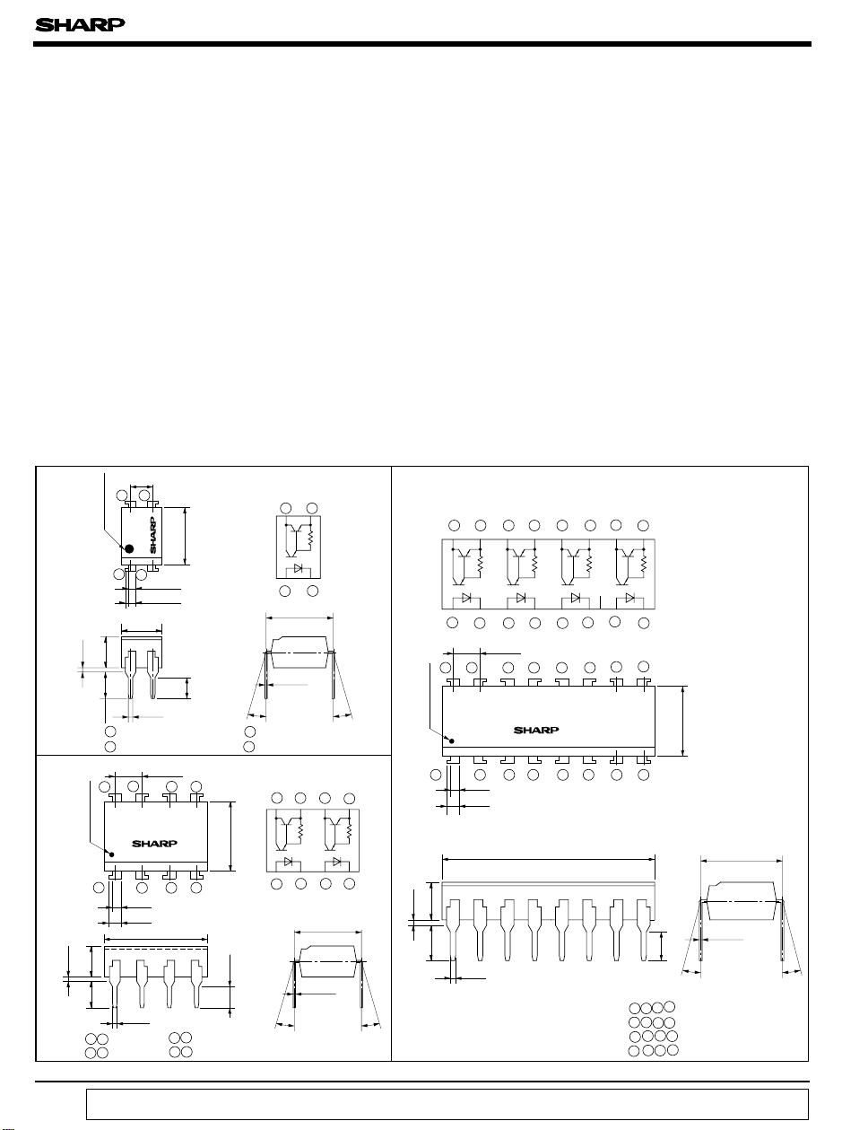
■ Outline Dimensions
PC865
PC875
TYP.
0.5
TYP.
0.5
Anode mark
± 0.5
3.5
± 0.5
3.0
1 3 Anode
2 4 Cathode
± 0.25
2.54
43
Anode mark
± 0.5
3.5
± 0.5
3.0
1 Anode
2 Cathode
1234
4.58
0.9
1.2
0.5
PC865
21
0.9
1.2
± 0.5
0.5
2.54
PC875
± 0.2
± 0.3
9.66
± 0.1
± 0.1
± 0.5
6.5
± 0.2
± 0.3
± 0.5
2.7
± 0.25
5678
± 0.5
5 7 Emitter
6 8 Collector
Internal connection
diagram
7.62
0.26
θ
= 0 to 13 ˚
3 Emitter
4 Collector
Internal connection
diagram
± 0.5
6.5
1234
± 0.5
2.7
34
12
± 0.3
± 0.1
7.62
0.26
θ
= 0 to 13 ˚
± 0.3
± 0.1
(
Unit : mm
PC895
θθ
5678
TYP.
0.5
θθ
Internal connection
diagram
12345678
± 0.25
2.54
0.9
1.2
0.5
± 0.2
± 0.3
± 0.1
PC895
19.82
± 0.5
Anode mark
1 2345678
± 0.5
3.5
± 0.5
3.0
10
111213141516
10
111213141516
1357 Anode
2468 Cathode
9 Emitter
10
9
9
11
12
13
14
± 0.5
6.5
± 0.5
2.7
θ
15
16
Collector
± 0.3
7.62
± 0.1
0.26
θ = 0 to 13 ˚
)
θ
“ In the absence of confirmation by device specification sheets, SHARP takes no responsibility for any defects that occur in equipment using any of SHARP's devices, shown in catalogs,
data books, etc. Contact SHARP in order to obtain the latest version of the device specification sheets before using any SHARP's device. ”
Page 2
PC865 Series
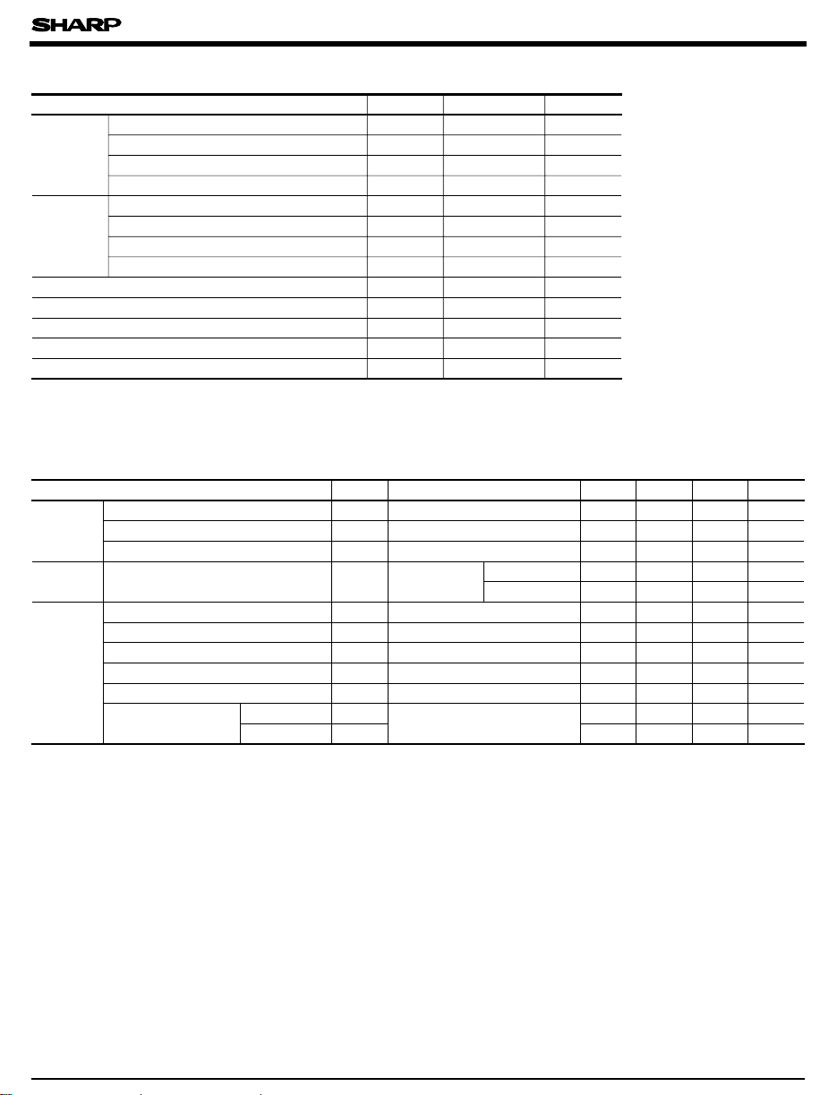
■ Absolute Maximum Ratings
Parameter Symbol Rating Unit
Forward current I
*1
Input
Peak forward current
Reverse voltage V
Power dissipation P 70 mW
Collector-emitter voltage V
Output
Emitter-collector voltage V
Collector current I
Collector power dissipation P
Total power dissipation P
*2
Isolation voltage
Operating temperature T
Storage temperature T
*3
Soldering temperature
*1 Pulse width <=100µ s, Duty ratio : 0.001
*2 40 to 60 % RH, AC for 1 minute
*3 For 10 seconds
■ Electro-optical Characteristics
Parameter Symbol Conditions MIN. TYP. MAX. Unit
Forward voltage V
Input
Output Collector dark current I
Transfer
characteristics
Reverse current I
Terminal capacitance C
Current transfer ratio CTR I
Collector-emitter saturation voltage
Isolation resistance R
Floating capacitance C
Cut-off frequency f
Response time
Rise time t
V
(
Ta = 25˚C
F
I
FM
R
CEO
ECO
C
C
tot
V
iso
opr
stg
T
sol
= 20mA - 1.2 1.4 V
FIF
VR=4V - - 10 µA
R
V= 0, f = 1kHz - 30 250 pF
t
VCE= 24V
CEO
CE(sat
=0
I
F
= 1mA, VCE=2V - %
F
)
IF= 20mA, IC= 5mA - 0.8 1.0 V
DC500V, 40 to 60 % RH
iso
V= 0, f = 1MHz - 0.6 1.0 pF
f
VCE= 2V, I
C
VCE= 2V, IC= 10mA
r
= 100 Ω
R
L
f
50 mA
1A
6V
70 V
0.1 V
80 mA
150 mW
200 mW
5 000
- 30 to + 100 ˚C
- 55 to + 125 ˚C
260 ˚C
Ta = 25˚C
Ta = 85˚C
= 2mA, R
CL
= 100 Ω, - 3dB
)
V
rms
--
--10-5A
1 000 8 000
5x101010
1 6 - kHz
- 100 300 µ s
- 35 200 µ sFall time t
11
(
Ta = 25˚C
2x10
- Ω
)
-7
A
Page 3

PC865 Serise
Fig. 1 Forward Current vs.
Ambient Temperature
60
50
)
40
mA
(
F
30
20
Forward current I
0
-30100 25 50 75 100 125
Ambient temperature Ta (˚C
)
Fig. 3 Peak Forward Current vs. Duty Ratio
10 000
5 000
)
2 000
mA
1 000
(
FM
500
200
100
50
20
Peak forward current I
10
5
-3
2
5
10
5
10
Duty ratio
-2
2
Pulse width <=100 µs
Ta= 25˚C
-1
2
5
10
1
5
Fig. 5 Current Transfer Ratio vs.
Forward Current
V
=2V
5 000
)
4 500
%
(
4 000
3 500
3 000
2 500
2 000
1 500
Current transfer ratio CTR
1 000
500
0
0.1
Forward current I
110
(mA)
F
CE
Ta= 25˚C
Fig. 2 Collector Power Dissipation vs.
Ambient Temperature
200
)
mW
(
150
C
100
50
Collector power dissipation P
0
-30
0 125
25 50 75 100
Ambient temperature T
(˚C)
a
Fig. 4 Forward Current vs. Forward Voltage
500
200
100
)
mA
(
F
Forward current I
T
= 75˚C
a
50˚C
25˚C
0˚C
50
- 25˚C
20
10
5
1
020.5 1.0 1.5 2.0 2.5 3.0 3.5
Forward voltage V
(V)
F
Fig. 6 Collector Current vs.
Collector-emitter Voltage
100
90
I
= 2mA
F
80
)
70
mA
(
C
60
50
40
30
Collector current I
20
10
0
0
1.5mA
1mA
0.7mA
0.5mA
12345
Collector-emitter voltage VCE (V
PC (MAX.
T
)
= 25˚C
a
)
Page 4

PC865 Serise
Fig. 7 Relative Current Transfer Ratio vs.
Ambient Temperature
130
)
%
100
(
IF= 1mA
=2V
V
CE
50
Relative current transfer ratio
0
-30
0 25 1007550
Ambient temperature T
(˚C)
a
Fig. 9 Collector Dark Current vs.
Ambient Temperature
-5
10
5
-6
10
)
5
A
(
-7
10
CEO
5
-8
10
5
-9
10
5
Collector dark current I
-10
10
5
-11
10
-30
Ambient temperature T
20
0
V
CE
40 60 80
(˚C)
a
= 20V
Fig.11 Frequency Response
0
)
dB
(
= 10kΩ
-10
R
L
1kΩ
100Ω
V
I
T
CE
= 2mA
C
= 25˚C
a
=2V
100
Fig. 8 Collector-emitter Saturation Voltage vs.
Ambient Temperature
1.3
)
1.2
V
(
)
1.1
sat
(
1.0
CE
I
= 20mA
F
I
= 5mA
C
0.9
0.8
0.7
0.6
0.5
0.4
0.3
0.2
Collector-emitter saturation voltage V
0.1
0
-30
25 50 75
0 100
Ambient temperature T (˚C)
a
Fig.10 Response Time vs. Load Resistance
1 000
t
r
)
100
µs
(
t
d
t
10
Response time
1
0.1
0.01 0.1 1 10 100
Load resistance R
V
=2V
CE
I
= 10mA
C
T
= 25˚C
L
a
(kΩ)
t
f
s
Test Circuit for Response Time
Input
V
CC
R
D
R
L
Output
Input
Output
t
t
s
d
r
10%
90%
tt
f
Voltage gain Av
-20
0.01 1
0.1
Frequency f (kHz
10 100
)
Test Circuit for Frepuency Response
V
CC
R
R
D
Output
L
Page 5

Fig.12 Collector-emitter Saturation
Voltage vs. Forward Current
10
)
9
V
(
)
8
sat
(
CE
7
6
5
4
3
2
1
Collector-emitter saturation voltage V
0
0
Please refer to the chapter “Precautions for Use”
●
I
= 0.1mA
C
1mA
5mA
10mA
30mA
12
Forward current I
50mA
F
(mA)
T
= 25˚C
a
PC865 Serise
 Loading...