

Page 1
High Collector-emitter Voltage
PC851
❈ Lead forming type (I type) and taping reel type (P type) are also available. (PC851I/PC851P)
Type Photocoupler
PC851
■ Features
1. High collector-emitter voltage
CEO
: 300V
(V
)
2. High isolation voltage between input and
output (V
: 5 000V
iso
)
rms
3. Compact dual-in-line package
4. Recognized by UL, file No. E64380
■ Applications
1. ON-OFF switching for transmission/reception
circuit for telephone
2. Interface to various power supply circuits,
power patch boards
3. Copiers, facsimiles
4. Output section for numerical control machines
5. Controller for SSRs, DC motors
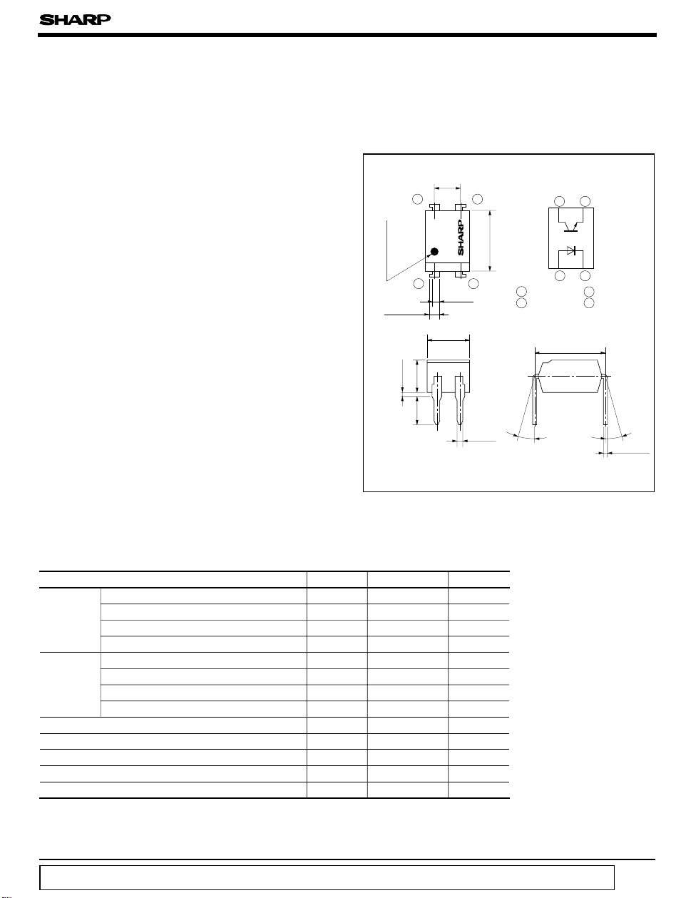
■ Outline Dimensions
± 0.25
2.54
4.58
PC851
0.9
± 0.5
± 0.2
0.5
3
± 0.5
6.5
2
± 0.1
4
Anode mark
1
± 0.3
1.2
TYP.
± 0.5
0.5
3.5
± 0.5
3.0
Internal connection
diagram
12
1 Anode
2 Cathode
7.62
θ
θ = 0 to 13 ˚
(
Unit : mm
34
3 Emitter
4 Collector
± 0.3
θ
0.26
)
± 0.1
■ Absolute Maximum Ratings
(
Ta= 25˚C
)
Parameter Symbol Rating Unit
Forward current I
*1
Input
Peak forward current I
Reverse voltage V
Power dissipation
Collector-emitter voltage V
Output
Emitter-collector voltage V
Collector current I
Collector power dissipation P
Total power dissipation
*2
Isolation voltage V
Operating temperature T
Storage temperature T
*3
Soldering temperature T
*1 Pulse width<=100µs, Duty ratio : 0.001
*2 40 to 60%RH, AC for 1 minute
*3 For 10 seconds
“ In the absence of confirmation by device specification sheets, SHARP takes no responsibility for any defects that occur in equipment using any of SHARP's devices, shown in catalogs,
data books, etc. Contact SHARP in order to obtain the latest version of the device specification sheets before using any SHARP's device.”
F
FM
R
P70mW
CEO
ECO
C
C
P
tot
iso
opr
stg
sol
50 mA
1A
6V
300 V
6V
50 mA
150 mW
200 mW
5 000
V
rms
- 25 to + 100 ˚C
- 55 to + 125 ˚C
260 ˚C
Page 2
PC851
■ Electro-optical Characteristics
Parameter Symbol Conditions MIN. TYP. MAX. Unit
Forward voltage V
Input
Output Collector dark current I
Transfer
charac-
teristics
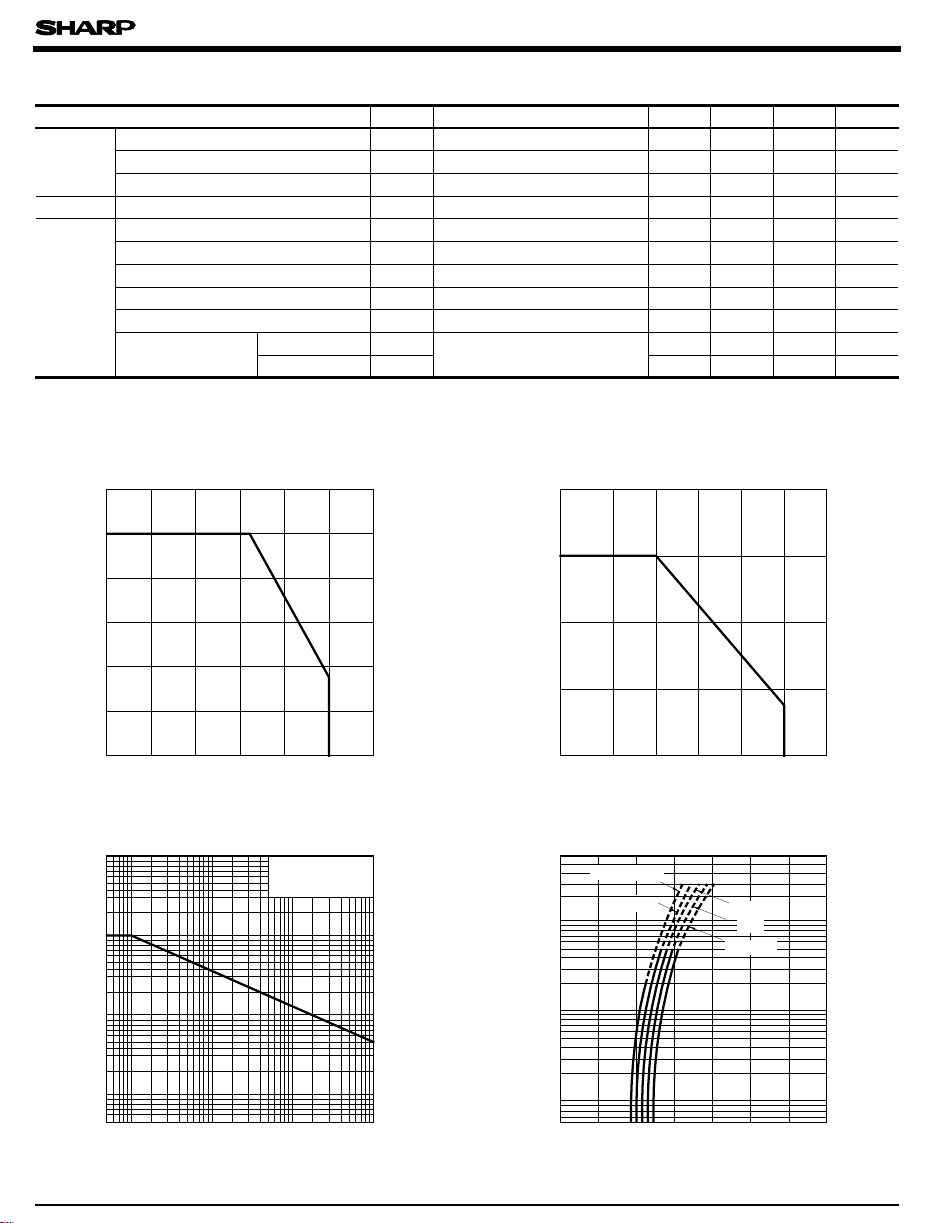
Fig. 1 Forward Current vs.
Ambient Temperature
)
mA
(
F
Forward current I
Reverse current I
Terminal capacitance C
Current transfer ratio CTR I
Collector-emitter saturation voltage
Isolation resistance R
Floating capacitance C V= 0, f = 1MHz - 0.6 1.0 pF
Cut-off frequency
Response time
60
50
40
20
10
Rise time
Fall time
R
CEO
V
CE(sat
ISO
f
C
t
r
t
f
= 20mA - 1.2 1.4 V
FIF
VR=4V - - 10 µA
V= 0, f= 1kHz - 30 250 pF
t
VCE= 200V, IF=0 - - 10
= 5mA, VCE=5V 40 80 - %
F
)
IF= 20mA, IC= 1mA - 0.1 0.3 V
DC500V, 40 to 60%RH
f
VCE= 5V, IC= 2mA, RL= 100Ω, - 3dB
VCE= 2V, IC= 2mA
= 100Ω
R
L
5x101010
- 50 - kHz
-410µs
-512µs
11
Fig. 2 Collector Power Dissipation vs.
Ambient Temperature
200
)
mW
(
150
C
100
50
Collector power dissipation P
(
Ta= 25˚C
-6
- Ω
)
A
0
-25300 25 50 75 100 125
Ambient temperature Ta (˚C
)
Fig. 3 Peak Forward Current vs. Duty Ratio
10 000
5 000
)
2 000
mA
1 000
(
FM
500
200
100
50
20
Peak forward current I
10
5
-3
2
5
10
5
10
Duty ratio
-2
2
Pulse width <=100µs
Ta= 25˚C
-1
2
5
10
5
1
0
-25
0 125
25 50 75 100
Ambient temperature Ta (˚C
)
Fig. 4 Forward Current vs. Forward Voltage
500
200
100
)
50
mA
(
F
20
10
5
Forward current I
1
020.5 1.0 1.5 2.0 2.5 3.0 3.5
= 75˚C
T
a
50˚C
Forward voltage VF (V
25˚C
0˚C
- 25˚C
)
Page 3

PC851
Fig. 5 Current Transfer Ratio vs.
Forward Current
100
VCE=5V
)
%
(
Ta= 25˚C
50
Current transfer ratio CTR
0
1
2
5
10 20 100
Forward current I
F
50
(mA)
Fig. 7 Relative Current Transfer Ratio vs.
Ambient Temperature
150
)
%
(
I
V
F
CE
= 5mA
=5V
100
50
Relative current transfer ratio
0
-25
0 25 50 75 100
Ambient temperature T
(˚C)
a
Fig. 9 Collector Dark Current vs.
Ambient Temperature
-5
10
-6
10
)
A
(
-7
10
CEO
-8
10
-9
10
-10
Collector dark current I
10
-11
10
-25
= 200V
V
CE
0
Ambient temperature T
25
50 75 100
(˚C)
a
Fig. 6 Collector Current vs.
Collector-emitter Voltage
= 25˚C
20
)
mA
(
C
10
Collector current I
0
0
I
= 30mA
F
25mA
20mA
15mA
10mA
5mA
Collector-emitter voltage V
510
P
CE
T
a
(MAX.
C
(V)
)
Fig. 8 Collector-emitter Saturation Voltage
vs. Ambient Temperature
0.16
I
= 20mA
F
I
= 1mA
C
0.14
)
V
(
)
0.12
sat
(
CE
0.10
0.08
0.06
0.04
0.02
0
Collector-emitter saturation voltage V
- 25 0 25 50 75 100
Ambient temperature T
(˚C)
a
Fig.10 Response Time vs. Load Resistance
500
V
=2V
CE
200
= 2mA
I
C
100
T
= 25˚C
a
50
)
µ s
20
(
10
5
2
Response time
1
0.5
0.2
0.1
0.01 0.1 1 10 50
Load resistance R
L
t
r
t
(k Ω
t
f
d
t
s
)
Page 4

Test Circuit for Response Time
Input
Output
t
Input
V
CC
Output
R
R
L
D
PC851
Fig.11 Frequency Response
V
=5V
CE
I
= 2mA
1kΩ
C
T
a
= 25˚C
100Ω
0
)
dB
(
10%
90%
t
d
s
tt
r
f
v
-10
Voltage gain A
R
L
= 10kΩ
-20
Fig.12 Collector-emitter Saturation
Voltage vs. Forward Current
6
)
V
(
)
5
sat
(
CE
4
3
2
7mA
5mA
3mA
1mA
= 0.5mA
I
C
1
Collector-emitter saturation voltage V
0
0
2 6 10 14 18
Forward current IF (mA
Please refer to the chapter “Precautions for Use ”
●
= 25˚C
T
a
20161284
)
0.5
1 2 5 10 50020010050
20
Frequency f (kHz
)
Test Circuit for Frepuency Response
V
CC
R
D
R
L
Output
 Loading...