

Page 1
PC812
PC812
High Noise Resistance Type
Photocoupler
■ Features
1. High noise reduction
(Common mode rejection voltage
: TYP. 1.5kV at dV/dt= 2kV/µs,
V
CM
RL= 470Ω, Vnp= 100mV
)
2. High current transfer ratio
(CTR : MIN. 90% at IF= 5mA, VCE=5V
3. High isolation voltage between input and
output (V
: 5 000V
iso
)
rms
4. Compact dual-in-line package
■ Applications
1. Motor-control circuits
2. Computer terminals
3. System appliances, measuring instruments
4. Signal transmission between circuits of
different potentials and impedances
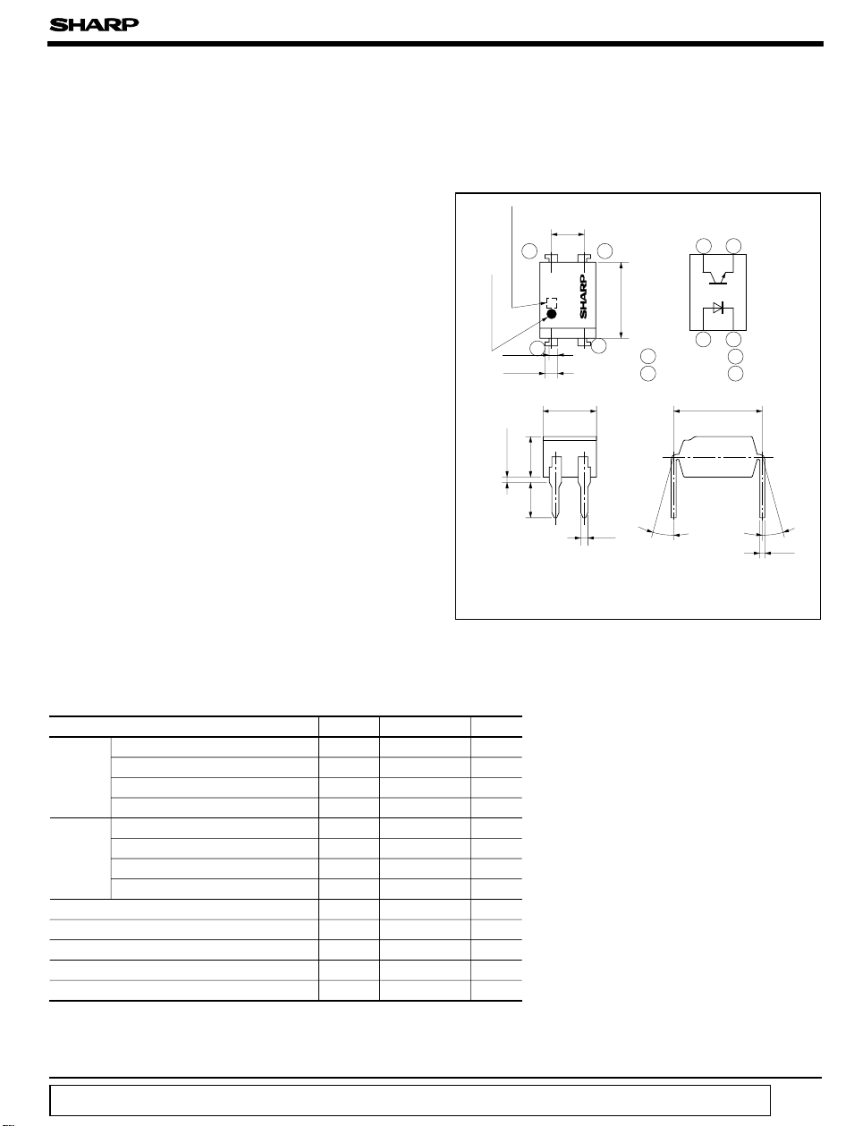
■ Outline Dimensions
± 0.25
2.54
PC812
± 0.5
2
0.5
3
± 0.5
6.5
± 0.1
1 Anode
2 Cathode
θ
4
CTR rank mark
)
Anode mark
1
± 0.2
0.9
± 0.3
1.2
4.58
± 0.5
0.5TYP.
3.5
± 0.5
3.0
(
Unit : mm
Internal connection
diagram
43
21
3 Emitter
4 Collector
7.62± 0.3
θ = 0 to 13 ˚
θ
0.26
)
± 0.1
■ Absolute Maximum Ratings
(
T
= 25˚C
a
)
Parameter Symbol Rating Unit
Input
Forward current I
*1
Peak forward current I
Reverse voltage V
F
FM
R
50 mA
1A
6V
Power dissipation P 70 mW
Collector-emitter voltage V
Output
Emitter-collector voltage V
Collector current I
Collector power dissipation P
Total power dissipation
*2
Isolation voltage
Operating temperature
Storage temperature
*3
Soldering temperature
*1 Pulse width<=100µs, Duty ratio : 0.001
*2 40 to 60%RH, AC for 1 minute
*3 For 10 seconds
“ In the absence of confirmation by device specification sheets, SHARP takes no responsibility for any defects that occur in equipment using any of SHARP's devices, shown in catalogs,
data books, etc. Contact SHARP in order to obtain the latest version of the device specification sheets before using any SHARP's device. ”
CEO
ECO
C
C
P
tot
V
iso
T
opr
T
stg
T
sol
35 V
6V
50 mA
150 mW
200 mW
5 000
V
- 30 to + 100
- 55 to + 125
260 ˚C
rms
˚C
˚C
Page 2
PC812
■ Electro-optical Characteristics
Parameter Symbol Conditions MIN. TYP. MAX. Unit
Forward voltage V
Input
Output Collector dark current I
Transfer
charac-
teristics
*4 Classification table of current transfer ratio is shown below.
Model
No.
PC812A A
PC812B B
PC812C C
PC812
Measurement
conditions
Peak forward voltage V
Reverse current I
Terminal capacitance C
*4
Current transfer ratio
Collector-emitter saturation voltage V
Isolation resistance R
Floating capacitance C
Cut-off frequency f
*4
Response time
*5
Common mode rejection voltage
Rank
mark
CTR (%
90 to 180
150 to 180
240 to 480
A, B or C
90 to 480
I = 5mA
VCE=5V
= 25˚C
T
a
Rise time
Fall time
)
t
(µ s
r
)
TYP.
MAX.
314416
416518
518720
418520
V
CE
= 2mA
I
C
R
L
T
= 25˚C
a
t
TYP.
=2V
= 100Ω
(µ s
f
(
Ta= 25˚C
= 20mA
I
F
F
= 0.5A
I
FM
FM
=4V
V
R
R
V = 0, f = 1kHz
t
= 20V, IF=0
V
CEO
CE
CTR 90 - 480 %
CE (sat
V
= 5mA, VCE=5V
I
F
)
= 20mA, IC= 1mA
I
F
DC500V, 40 to 60%RH
ISO
V = 0, f = 1MHz
f
VCE= 5V, IC= 2mA, RL= 100Ω , - 3dB
c
t
r
VCE= 2V, IC= 2mA, RL= 100Ω
t
f
CM
dV/dt= 2kV/ µ s, R
= 470Ω, Vnp= 100mV, IF=0
L
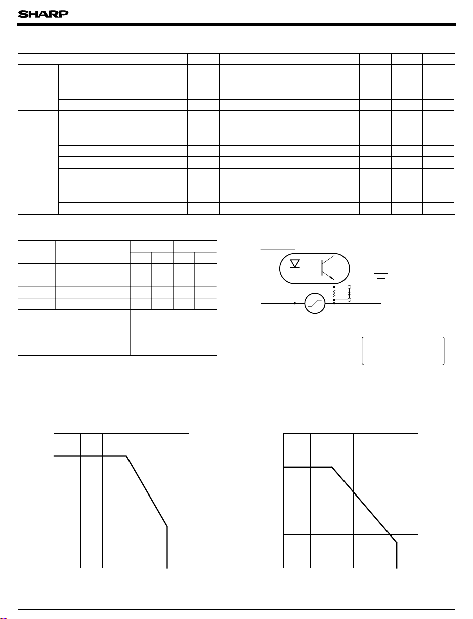
*5 Test Circuit for V
- 1.2 1.4 V
- - 3.0 V
--10µA
-30 pF
200
--10-7A
- 0.1 0.2 V
5x101010
11
- Ω
- 0.6 1.0 pF
15 80 - kHz
-418µs
-520µs
- 1.5 - k V
CM
)
MAX.
V
= 9V
CC
R
V
L
np
V
CM
VCM: Common mode rejection
voltage
(higher value of pulse wave
dV/dt: Rising factor of voltage
)
Test condition
= 100mV, RL= 470Ω
V
np
dV/dt = 2kV/µ s, IF= 0
)
Fig. 1 Forward Current vs.
Ambient Temperature
60
50
)
40
mA
(
F
30
20
Forward current I
0
-30100 25 50 75 100 125
Ambient temperature Ta (˚C
Fig. 2 Collector Power Dissipation vs.
Ambient Temperature
200
)
mW
(
C
150
100
50
Collector power dissipation P
0
-30
)
0 125
25 50 75 100
Ambient temperature Ta (˚C
)
Page 3

PC812
Fig. 3 Peak Forward Current vs. Duty Ratio
10 000
5 000
)
mA
2 000
(
1 000
FM
500
200
100
50
Peak forward current I
20
10
5
-3
2
5
10
5
-2
2
10
Duty ratio
Pulse width<=100µs
Ta= 25˚C
-1
2
5
5
10
1
Fig. 5 Current Transfer Ratio vs.
Forward Current
500
400
)
%
(
300
200
100
Current transfer ratio CTR
V
T
=5V
CE
= 25˚C
a
Fig. 4 Forward Current vs. Forward Voltage
500
200
100
)
mA
(
F
Forward current I
T
= 75˚C
a
50˚C
25˚C
0˚C
50
- 25˚C
20
10
5
1
020.5 1.0 1.5 2.0 2.5 3.0 3.5
Forward voltage V
(V)
F
Fig. 6 Collector Current vs.
Collector-emitter Voltage
40
35
)
30
mA
(
C
25
20
15
Collector current I
10
= 30mA
I
F
20mA
10mA
P
5mA
(MAX.
C
T
)
= 25˚C
a
0
1
2
Forward current I
10 20 50
5
F
(mA)
Fig. 7 Relative Current Transfer Ratio vs.
Ambient Temperature
150
)
%
(
100
50
Relative current transfer ratio
0
0255075
-30
Ambient temperature T
I
= 5mA
F
=5V
V
CE
100 125
(˚C)
a
0
051
Fig. 8 Collector-emitter Saturation Voltage
vs. Ambient Temperature
0.16
)
V
(
0.14
)
sat
(
CE
0.12
2345678910
I
= 20mA
F
= 1mA
I
C
(V)
CE
Collector-emitter voltage V
0.10
0.08
0.06
0.04
0.02
Collector emitter saturation voltage V
0
-30
0 20406080100
Ambient temperature T
(˚C)
a
Page 4

PC812
Fig. 9 Collector Dark Current vs.
Ambient Temperature
-6
10
VCE= 20V
5
-7
10
)
A
5
(
-8
10
CEO
5
-9
10
5
-10
10
5
Collector dark current I
-11
10
5
-12
10
-30
0
20
40 60 80
Ambient temperature T
100
a
Fig.11 Frequency Response
0
)
-5
dB
(
v
-10
-15
Voltage gain A
RL= 10kΩ
(˚C)
120 140
V
I
T
1kΩ
CE
= 2mA
C
a
=5V
= 25˚C
100Ω
Fig.10 Response Time vs. Load Resistance
500
VCE=2V
200
= 2mA
I
C
100
= 25˚C
T
a
50
)
µs
(
20
10
5
2
Response time
1
t
f
t
t
d
r
t
s
0.5
0.2
0.1
0.01 0.1 1 10 50
)
Load resistance R
(kΩ
L
Test Circuit for Response Time
Input
Output
t
t
s
d
r
Input
V
CC
Output
R
R
L
D
10%
90%
tt
f
-20
0.5 1 2 5 2001005020
10
Frequency f (kHz
)
Fig.12 Collector-emitter Saturation Voltage vs.
Forward Current
8
)
V
(
)
7
sat
(
CE
6
I
= 0.5mA
C
5
4
3
2
1
Collector-emitter saturation voltage V
0
0
246810
Forward current I
1mA
3mA
5mA
7mA
F
(mA)
T
= 25˚C
a
97531
500
Test Circuit for Frepuency Response
V
CC
R
D
Please refer to the chapter
●
R
L
Output
“Precautions for Use ”
 Loading...