

Page 1
High Input Current, AC Input
PC733H
❈ Lead forming type (I type) and taping reel type (P type) are also available. (PC733HI/PC733HP)
Type Photocoupler
PC733H
■ Features
1. AC input response
2. High input current (IF: MAX. 150mA
3. High isolation voltage between input and
output
(V
: 5 000 V
iso
)
rms
4. Low collector dark current
(I
: MAX. 10-7A at VCE= 20V
CEO
)
5. TTL compatible output
6. Recognized by UL, file No. E64380
■ Aapplications
1. Telephone sets
2. System appliances, measuring instruments
3. Signal transmission between circuits of
different potentials and impedances
■ Absolute Maximum Ratings
Parameter Symbol Rating Unit
Forward current I
Input
Output
*1 Pulse width<=100µs, Duty ratio: 0.001
*2 40 to 60%RH, AC for 1 minute
*3 For 10 seconds
*1
Peak forward current I
Power dissipation P 230 mW
Collector-emitter voltage V
Emitter-collector voltage V
Collector-base voltage V
Emitter-base voltage V
Collector current I
Collector power dissipation P
Total power dissipation
*2
Isolation voltage
Operating temperature
Storage temperature
*3
Soldering temperature
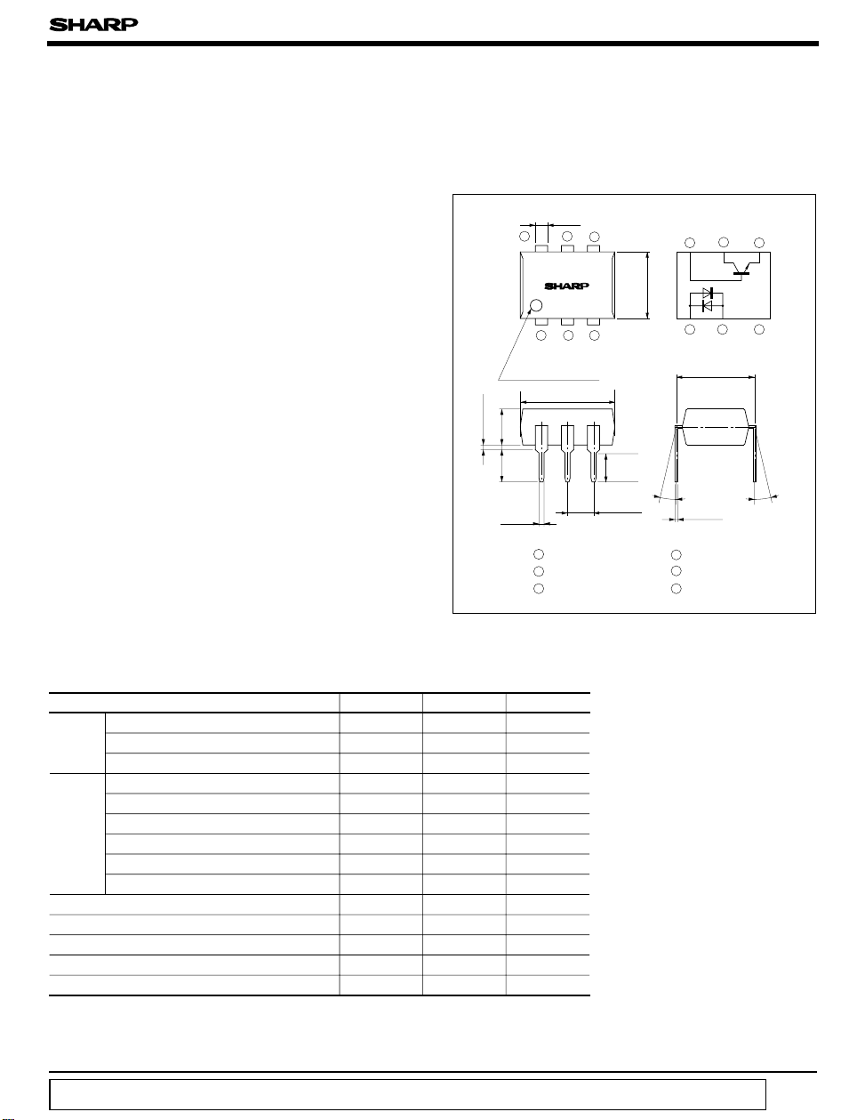
■ Outline Dimensions
± 0.3
)
± 0.5
0.5TYP.
± 0.5
F
FM
CEO
ECO
CBO
EBO
C
C
P
tot
V
iso
T
opr
T
stg
T
sol
± 150 mA
±1 A
35 V
6V
35 V
6V
80 mA
160 mW
320 mW
5 000
- 25 to + 100
- 55 to + 125
260 ˚C
1.2
PC733H
123
Primary side mark
(
Sunken place
9.22
3.5
3.7
± 0.1
0.5
1 Anode, cathode
2 Anode, cathode
3 NC
(
Ta= 25˚C
V
rms
˚C
˚C
± 0.5
± 0.5
± 0.25
diagram
± 0.5
6.5
θ
456
)
3.4
2.54
)
(
Unit : mm
Internal connection
654
± 0.3
7.62
± 0.1
0.26
θ = 0 to 13 ˚
4 Emitter
5 Collector
6 Base
321
)
θ
“ In the absence of confirmation by device specification sheets, SHARP takes no responsibility for any defects that occur in equipment using any of SHARP's devices, shown in catalogs,
data books, etc. Contact SHARP in order to obtain the latest version of the device specification sheets before using any SHARP's device. ”
Page 2
PC733H
■ Electro-optical Characteristics
Parameter Symbol Conditions MIN. TYP. MAX. Unit
Forward voltage V
Input
Peak forward voltage V
Terminal capacitance C
Output Collector dark current I
Current transfer ratio CTR
Collector-emitter saturation voltage
Transfer
characteristics
Isolation resistance R
Floating capacitance C
Cut-off frequency f
Response time
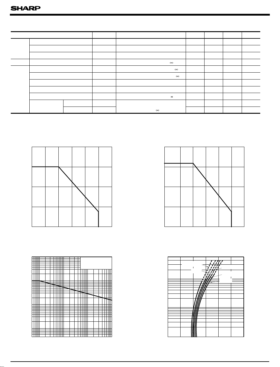
Fig. 1 Forward Current vs.
Ambient Temperature
200
150
)
mA
(
F
100
Rise time
Fall time
V
F
FM
CEO
CE(sat
ISO
c
t
r
f
IF= ±100mA - 1.4 1.7 V
IFM= ±0.5A - - 3.0 V
V= 0, f = 1kHz - 50 400 pF
t
VCE= 20V, IF= 0, RBE=--10-7A
IF= ±100mA, VCE= 2V, RBE=
)
IF= ±100mA, IC= 1mA, RBE=
DC500V, 40 to 60%RH
V= 0, f=1MHz
f
VCE= 5V, IC= 2mA, RL= 100 Ω, RBE= , - 3dB
VCE= 2V, IC= 2mA,
=100Ω, RBE=
R
L
20 - 80 %
- 0.1 0.2 V
5x101010
11
- 0.6 1.0 pF
15 80 - kHz
-418µs
-318µst
Fig. 2 Collector Power Dissipation vs.
Ambient Temperature
200
)
160
mW
150
(
C
100
(
Ta= 25˚C
- Ω
)
Forward current I
0
-25500 25 50 75 100 125
Ambient temperature T
a
(˚C
)
Fig. 3 Peak Forward Current vs. Duty Ratio
10 000
5 000
)
2 000
mA
1 000
(
FM
500
200
100
50
20
Peak forward current I
10
-3
222
5555
10
10
-2
Duty ratio
Pulse width<=100
Ta= 25˚C
-1
10
µ s
1
50
Collector power dissipation P
0
-25
0 125
25 50 75 100
Ambient temperature T
a (˚C
)
Fig. 4 Forward Current vs. Forward Voltage
500
200
)
100
mA
(
50
F
20
10
5
Forward current I
2
1
0
Ta= 75˚C
50˚C
0.5 1.0 1.5 2.0 2.5 3.0
Forward voltage V
25˚C
- 25˚C
(V
F
0˚C
)
Page 3

PC733H
Fig. 5 Current Transfer Ratio vs.
Forward Current
80
70
)
%
(
60
50
=2V
V
CE
R
=
BE
Ta= 25˚C
Fig. 6 Collector Current vs.
Collector-emitter Voltage
)
mA
(
C
50
40
= 150mA
I
F
30
P
100mA
C
(
MAX.
40
30
20
Current transfer ratio CTR
10
0
0.1
0.2
1 2 5 10 20 50 200100
0.5
Forward current I
(mA
F
)
Fig. 7 Relative Current Transfer Ratio vs.
Ambient Temperature
150
)
%
(
100
I
= 100mA
F
R
BE
V
CE
=
=2V
20
50mA
Collector current I
10
0
0
20mA
10mA
246810
Collector-emitter voltage V
Fig. 8 Collector-emitter Saturation Voltage
vs. Ambient Temperature
)
mV
(
)
sat
(
CE
160
140
120
100
IF= 100mA
I
= 1mA
C
R
=
BE
80
50
60
40
Relative current transfer ratio
0
0 25 50 75 100
-25
Ambient temperature T
(˚C)
a
Fig. 9-a Collector Dark Current vs.
Ambient Temperature Ambient Temperature
-5
10
10
)
A
(
10
CEO
10
10
Collector dark current I
10
10
= 20V
V
CE
R
=
BE
-6
-7
-8
-9
-10
-11
-25
25
0
50 75
Ambient temperature Ta(˚C)
100
20
0
Collector-emitter saturation voltage V
- 25 0 25 50 75 100
Ambient temperature T
Fig. 9-b Collector-base Dark Current vs.
-8
10
VCB= 30V
R
=
5
)
A
(
CBO
10
Collector-base dark current I
10
BE
2
-9
10
5
2
-10
5
2
-11
0
25
Ambient temperature Ta (˚C
50 75 100
)
R
=
BE
= 25˚C
T
a
(V)
CE
(˚C)
a
125
)
Page 4

PC733H
Fig.10 Response Time vs. Load Resistance
200
V
=2V
CE
100
= 2mA
I
C
50
20
)
µs
(
10
Response time
5
2
1
=
R
BE
Ta= 25˚C
t
f
t
d
t
r
0.5
0.2
t
s
0.1
0.1 1 100.03 0.2 0.5 2 5
Load resistance R
L
(kΩ)
Test Circuit for Response Time
Input
Output
t
t
d
t
r
Input
V
CC
R
L
R
D
Output
Test Circuit for Frequency Response
V
CC
R
R
D
L
Output
Fig.11 Frequency Response
=5V
V
CE
I
= 2mA
0
)
-5
dB
(
v
-10
-15
Voltage gain A
R
= 10kΩ
L
1kΩ
C
=
R
BE
Ta= 25˚C
100Ω
-20
0.5 1 2 5
10
Frequency f (kHz
2001005020
500
1 000
)
Fig.12 Collector-emitter Saturation Voltage
vs. Forward Current
10
)
V
(
9
)
sat
(
8
CE
7
10%
90%
s
t
f
6
5
4
3
2
1
Collector-emitter saturation voltage V
0
0
IC=1mA
2mA
RBE=
T
= 25˚C
a
3mA
5mA
7mA
10mA
40mA
30mA
20mA
20 40 60 80 100
Forward current I
F
(mA)
9070503010
● Please refer to the chapter “Precautions for Use ”
.
 Loading...