

Page 1
PC512
PC512
European Safety Standard
Approved Long Creepage
Distance Type Photocoupler
■ Features
1. Conform to European Safety Stndards
UL file No. E64380
Approved by VDE (DIN VDE0884 : No. 77296
Approved by BSI
(
BS EN60065 IEC65 Test Leaf lets land 5
BS EN60950 IEC950 EN41003 Test Leaflets land 5
Approved by SEMKO (No. 9303001
Approved by DEMKO (108025
Approved by EI (155031-01
Approved by CSA (CA95323 or CA76261
)
)
)
)
2. Long creepage distance type
(Creepage distance : 11.5mm or more
)
3. Compact
4. High isolation voltage (V
: 5 000V
iso
)
rms
■ Applications
1. Power supplies
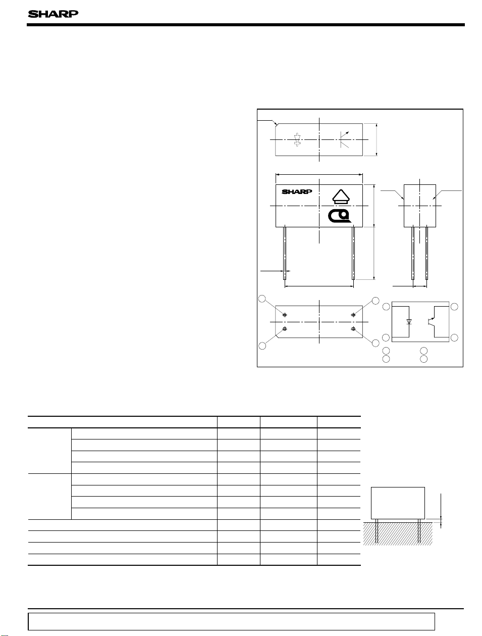
± 0.2
6.0
Marking
face
± 0.2
8.0
)
10.0
(
(
2.54
1
2
1 Anode
2 Cathode
(
Unit : mm
)
3 Collector
4 Emitter
■ Outline Dimensions
C0.7
)
± 0.2
16.2
)
PC512
4 - 0.4
(
12.7
2
1
( )
: Reference dimensions
4
V
D E
)
3
4
Resin
package
4
3
)
■ Absolute Maximum Ratings
(
Ta = 25˚C
)
Parameter Symbol Rating Unit
Forward current
*1
Input
Peak forward current
Reverse voltage V
Power dissipation
Collector-emitter voltage V
Output
Emitter-collector voltage 6 V
Collector current
Collector power dissipation
*2
Isolation voltage
Operating temperature T
Storage temperature
*3
Soldering temperature
*1 Pulse width<=100µs Duty ratio : 0.001
*2 AC for 1minute, 40 to 60%RH
*3 For MAX. 10 seconds at the position of 1mm from the edge of resin package.
“ In the absence of confirmation by device specification sheets, SHARP takes no responsibility for any defects that occur in equipment using any of SHARP's devices, shown in catalogs,
data books, etc. Contact SHARP in order to obtain the latest version of the device specification sheets before using any SHARP's device.”
I
F
I
FM
R
P75mW
CEO
V
ECO
I
C
P
C
V
iso
opr
T
stg
T
sol
50 mA
1A
6V
35 V
20 mA
75 mW
5kV
rms
- 25 to+ 85 ˚C
- 40 to+ 100 ˚C
260 ˚C
Soldering area
1mm
Page 2
PC512
■ Electro-optical Characteristics
Forward voltage
Input
Output
Transfer
characteristics
Peak forward voltage
Reverse current
Terminal capacitance
Collector dark current
Collector-emitter breakdown voltage
Emitter-collector breakdown voltage
Collector current
Collector-emitter saturation voltage
Isolation resistance
Cut-off frequency
Response time
Rise time
Fall time
Symbol Conditions MIN. TYP. MAX. UnitParameter
V
F
V
FM
I
R
C
t
I
CEO
BV
CEO
BV
ECOIE
I
C
V
CE(sat
R
iso
f
c
t
r
t
f
(
IF= 20mA - 1.2 1.4 V
IFM= 0.5A - 3 4 V
VR=3V
V= 0, f= 1kH
Z
VCE= 20V, IF= 0 - - 100 nA
= 0.1mA, IF=0
I
C
=10µA, IF=0 6 - - V
IF= 20mA, VCE=5V 2 - 20 mA
)
= 40mA, IC= 1mA - - 0.4 V
I
F
DC500V, 40 to 60%RH 10
V
= 2V, IC= 2mA
CE
= 100Ω, - 3dB
R
L
VCE= 2V, IC= 2mA
= 100Ω
R
L
--10µA
- 50 250 pF
35 - - V
12
--Ω
12 80 - kH
-320
-430
Ta= 25˚C
µs
µs
)
Z
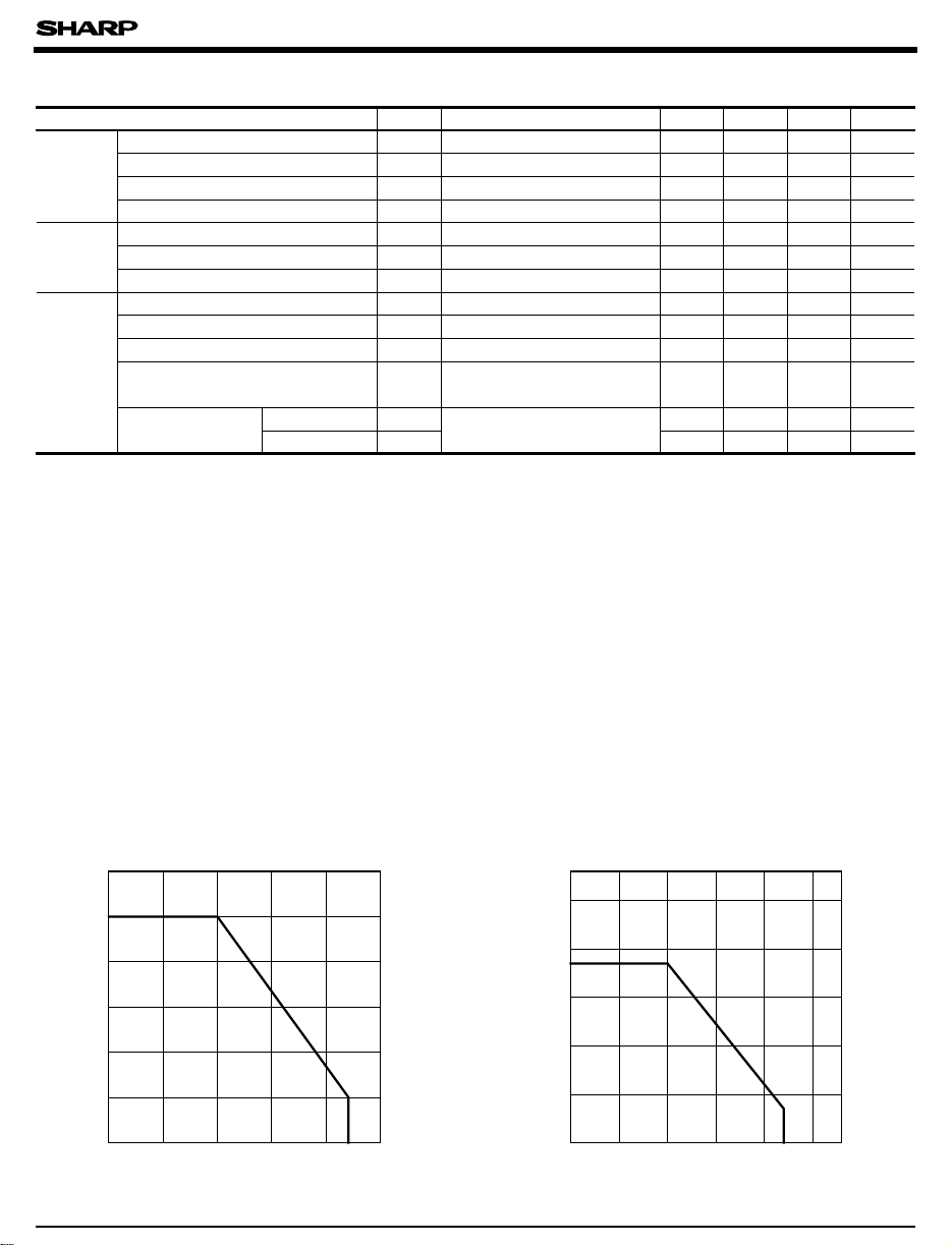
Fig. 1 Forward Current vs. Ambient
Temperature
60
50
)
40
mA
(
F
30
20
Forward current I
10
0
- 25 0 25 50 75 10085
Ambient temperature T
)
(˚C
a
Fig. 2 Collector Power Dissipation vs.
Ambient Temperature
100
)
80
mW
75
(
60
40
20
Collector power dissipation
0
Ambient temperature Ta (˚C
85- 25 0 25 50
75 100
)
Page 3

PC512
Fig. 3 Peak Forward Current vs. Duty Ratio
Pulse width<=100 µ s
Ta= 25˚C
5000
)
mA
(
1000
FM
500
100
50
Peak forward current I
10
-3
10
-2
10
Duty ratio
-1
10
10
Fig. 5 Current Tranfer Ratio vs.
Forward Current
70
60
)
50
%
(
40
30
20
Current tranfer ratio CTR
10
0
0.1 1 10 100
Forward current IF (mA
VCE=5V
= 25˚C
T
a
)
Fig. 4 Forward Current vs. Forward Voltage
100
50
)
20
mA
(
F
10
5
Forward current I
2
0
1
25˚C
50˚C
75˚C
Forward voltage V
0˚C
- 25˚C
)
(V
F
3.02.52.01.51.00.50.0
Fig. 6 Collector Current vs. Collector
-emitter Voltage
T
= 25˚C
20
)
16
mA
(
C
12
8
Collector current I
4
0
0246
Collector-emitter voltage VCE (V
Pc
IF= 30mA
(
max
20mA
a
)
10mA
5mA
810
)
Fig. 7 Relative Current Transfer Ratio vs.
Ambient Temperature
150
)
%
100
(
50
Relative current transfer ratio
0
-25
0 25 50 75 100
Ambient temperature Ta (˚C
IF= 20mA
VCE=5V
)
Fig. 8 Collector-emitter Saturation Voltage vs.
Ambient Temperature
0.16
I
= 40mA
F
I
= 1mA
C
0.14
0.12
0.10
0.08
0.06
)
V
(
)
0.04
sat
(
CE
0.02
Collector-emitter saturation voltage
V
0.00
-25
0 255075100
)
Ambient temperature T
(˚C
a
Page 4

PC512
Fig. 9 Collector Dark Current vs.
Ambient Temperature
-6
10
)
A
10
(
CEO
10
10
Collector dark current I
10
VCE= 20V
5
2
-7
5
2
-8
5
2
-9
5
2
-10
0255075
Ambient temperature T
(˚C)
a
100
Fig.10 Response Time vs. Load Resistance
1000
500
200
100
)
µs
(
Response time
=2V
V
CE
I
= 2mA
C
T
= 25˚C
a
50
20
10
5
2
1
t
r
t
f
t
d
t
s
0.5
0.2
0.1
1010.10.01
Load resistance R kL ( Ω
)
100
Fig.11 Frequency Response Fig.12 Collector-emitter Saturation Voltage
vs. Forward Current
5
0
)
dB
(
-5
V
-10
Voltage gain A
-15
-20
0.1 1 10
RL= 10k Ω
Frequency(kHz
VCE=5V
I
= 2mA
C
= 25˚C
T
a
1kΩ
100
)
100Ω
1000
6
I
4.8
C
3.6
2.4
)
V
(
)
sat
(
1.2
CE
Collector-emitter saturation voltage
V
0
02468
Forward current I
F
T
= 0.5mA
1mA
3mA
5mA
7mA
(mA)
= 25˚C
a
10
Please refer to the chapter “Precautions for Use ”
●
 Loading...