

Page 1
PC417
PC417
Compact, Surface Mount
Ultra-high Speed Response
OPIC Photocoupler
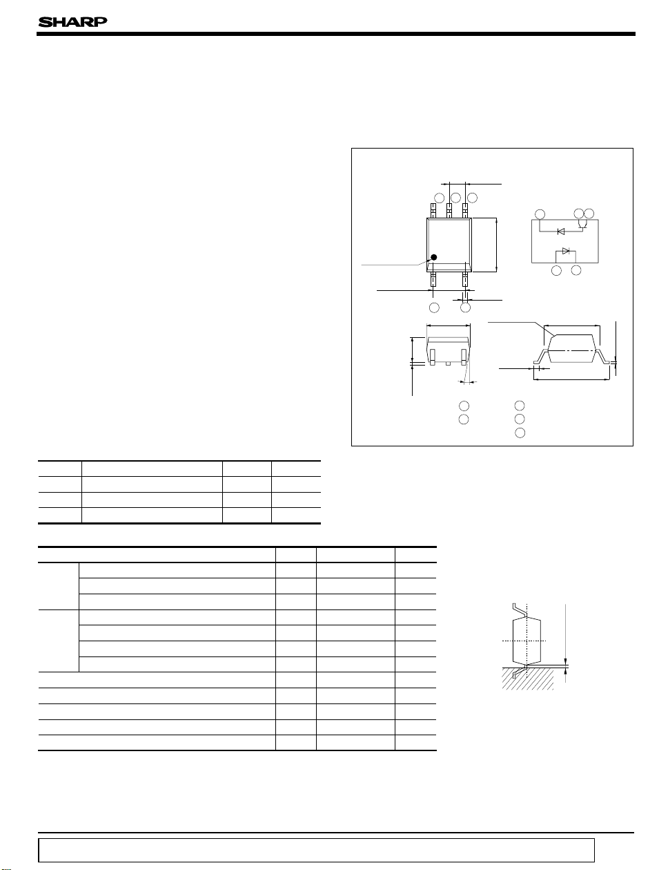
■ Features ■ Outline Dimensions
1. Mini-flat package
2. Ultra-high speed response
(t
PHL
, t
: TYP. 0.3µs at RL= 1.9kΩ
PLH
)
3. Isolation voltage between input and output
)
(V
: 2 500 V
iso rms
4. High instantaneous common mode rejec-
tion voltage (CMH: TYP. 1kV/µs
5. Recognized by UL(No.64380)
■ Applications
)
Anode mark
± 0.25
2.5
13
1. Hybrid substrate which requires high den sity mounting
2. Personal computers, office computers and
peripheral equipment
3. Audio equipment
■ Package Specifications
Model No.
PC417 φ 370mm 12mm
PC417T φ 178mm 12mm
PC417Z --
Package specifications
Taping package(Net:3 000pcs.
Taping package(Net: 750pcs.
Sleeve package(Net: 100pcs.
)
)
)
Diameter of reel
Tape width
* “OPIC ” (Optical IC) is a trademark of the SHARP Corporation.
An OPIC consists of a light-detecting element and signal processing circuit integrated onto a single chip.
■ Absolute Maximum Ratings
Parameter Symbol Rating Unit
*1
Forward current
Input
Reverse voltage V
Power dissipation
*2
Supply voltage
Output
Output voltage
Output current
Power dissipation
Total power dissipation
*3
Isolation voltege
Operating temperature T
Storage temperature T
*4
Soldering temperature
*1 Ta= 0 to+ 70˚C
*2 For 1 minute max.
*3 40 to 60% RH, For AC 1 minute, Apply the specified voltage between the whole of the electrode pins on the input
side and the whole of the electrode pins on the output side.
*4 For 10 seconds.
I
F
R
PmW
V
CC
V
O
I
O
P
O
P
tot
V
iso
opr
stg
T
sol
25
5
45
- 0.5 to + 15
- 0.5 to + 15
8
100
100
2 500
- 40 to + 100
- 40 to + 125
260 ˚C
± 0.2
2.6
± 0.1
0.1
(
Ta= 25˚C
mW
mW
V
)
mA
V
V
V
mA
rms
˚C
˚C
6
PC417
3.6
1.27
45
0.4
± 0.3
6˚
1 Anode
3 Cathode
± 0.25
± 0.2
4.4
± 0.1
C0.4
(
Input Side
+ 0.4
0.5
- 0.2
4 GND
5 V
6 V
Soldering area
(
Unit : mm
internal connection
diagram
4
56
1
3
± 0.3
5.3
)
+ 0.2
7.0
- 0.7
O
CC
0.2mm or more
)
± 0.05
0.2
“ In the absence of confirmation by device specification sheets, SHARP takes no responsibility for any defects that occur in equipment using any of SHARP's devices, shown in catalogs,
data books, etc. Contact SHARP in order to obtain the latest version of the device specification sheets before using any SHARP's device.”
Page 2
PC417
■ Electro-optical Characteristics
Parameter Symbol Conditions MIN. TYP. MAX. Unit
Forward voltage V
Input
Reverse current I
Terminal capacitance C
I
I
I
CCH(1
I
CCH(2
I
V
OH(1
OH(2
OH(3
Output
High level output
current I
High level supply
current
Low level supply
current
Low level output
voltage
Current transfer ratio CTR
Isolation resistance R
Floating capacitance C
*6
Transfer
charac-
teristics
“H→L” propagation delay
time
*6
“L→H” propagation delay
time
*7
Instantaneous common
mode rejection voltage
t
t
CM
“High level output”
*7
Instantaneous common
mode rejection voltage
CM
“Low level output”
*5 Temperature range : Ta= 0 to 70˚C
*6 Test circuit for propagation delay time is shown in the next page.
*7 Test circuit for instantaneous common mode rejection voltage is shown in the next page.
Each characteristics shall be measured under opaque condition.
= 16mA
I
F
F
=5V
V
R
R
= 0, f = 1MH
V
t
F
IF=0, VCC=5.5V
)
=5.5V
V
O
)
=0, V
I
)
I
)
IF=0, V
IF= 0, VCC= 15V, VO= OPEN *5
)
IF=16mA, VCC=15V
CCL
VO=OPEN *5
I
OL
I
I
V
DC500V, 40 to 60%RH
ISO
V=0V, f=1MHz
f
PHL
IF=16mA, VCC=5V
R
PLH
I
V
H
V
I
V
L
V
=15V, V
F
CC
=0, VCC=15V, VO=15V *5
F
=15V, V
CC
=16mA, VCC=4.5V
F
=2.4mA *5
O
=16mA, VCC=4.5V
F
=0.4V,*5
O
=1.9kΩ
L
=0, RL=1.9kΩ
F
=10V
=5V
=10V
=5V
,
P-P
,
P-P
CM
CC
=16mA, RL=1.9kΩ
F
CM
CC
Z
O
O
=15V
=OPEN
(
Ta= 25˚C
- 1.7 1.95 V
--10µA
- 60 250
pF
- 3 500 nA
- - 1.0
--50
- 0.02 1.0
- - 2.0
µA
µA
- 200 - µ A
- - 0.4 V
19 - - %
10
5x10
-
-
11
10
- Ω
0.6 1.0 pF
0.3 0.8
µ s
- 0.3 1.2
- 1 000 - V/ µ s
- - 1 000 - V/ µ s
)
Page 3

*6 Test Circuit for Propagation Delay Time
F
Pulse input
Pulse width
10µs
Duty radio
1/10
F
I
monitor
I
1
3
100Ω
CC
V
=5V
6
L
R
5
4
0.01
µF
C
O
V
L
=15pF
*7 Test Circuit for Instantaneous Common Mode Rejection Voltage
F
I
SW
A
1
B
FF
V
3
+-
CM
V
CC
=5V
V
6
L
R
5
O
V
0.01µF
V
CM
4
CM
F
I
0
O
V
CM
0V
when GLSW is A
H
O
V
IF=0mA
when GLSW is B
L
O
V
F
I
=16mA
PC417
5V
f
90%
0.8V
1.5V
OL
V
t
PLH
10%
90%
r
t
2V
5V
OL
V
1.5V
t
PHL
10V
10%
t
Fig. 1 Forward Current vs.
Ambient Temperature
30
)
20
mA
(
F
10
Forward Current I
0
-40
0 25 50 75 100 125
Ambient temperature Ta (˚C
Fig. 2 Power Dissipation vs.
Ambient Temperature
120
P
100
)
mW
80
(
O
60
45
40
Power dissipation P, P
20
0
-40
0 25 50 75 100 125
)
O
P
Ambient temperature Ta (˚C
)
Page 4

Fig. 3 Forward Current vs. Fig. 4 Output Current vs. Output Voltage
Forward Voltage
100
)
10
mA
(
F
1
Forward current I
0.1
Ta= 0˚C
25˚C
50˚C
70˚C
20
V
18
T
16
)
14
mA
(
12
O
10
8
6
Output current I
4
CC
= 25˚C
a
=5V
Dotted line shows
pulse characteristics
= 25mA
I
F
20mA
15mA
10mA
5mA
PC417
0.01
1.0
1.2 1.4 1.6 1.8 2.0 2.2
Forward voltage VF (V
)
0
022
4 6 8 10 12 14 16 18 20
Output voltage VO (V
)
Fig. 5 Relative Current Transfer Ratio vs. Fig. 6 Relative Current Transfer Ratio vs.
Forward Current
150
)
%
(
100
50
Relative current transfer ratio
0
0.1
1 10 100
Forward current IF (mA
CTR= 100% at
I
= 16mA
F
V
V
T
)
CC
= 0.4V
O
= 25˚C
a
=5V
Ambient Temperature
110
)
100
%
(
90
80
70
Relative current transfer ratio
CTR= 100% at T
60
-60 -40 -20
0 20 40 60 80 100
Ambient temperature Ta (˚C
I
F
V
O
V
CC
= 16mA
= 0.4V
=5V
= 25˚C
a
)
Fig. 7 Propagation Delay Time vs. Fig. 8 High Level Output Current vs.
Ambient Temperature
800
)
ns
(
600
PLH
, t
PHL
400
200
Propagation delay time t
0
- 60 - 20 20 60 10080400-40
Ambient temperature Ta (˚C
I
= 16mA
F
=5V
V
CC
RL= 1.9kΩ
t
PHL
t
PLH
)
Ambient Temperature
-5
10
-6
10
)
A
(
-7
OH
10
-8
10
-9
10
-10
10
High level output current I
-11
10
- 60 - 40 - 20 0 20 100806040
Ambient temperature Ta (˚C
VCC=VO=5V
)
Page 5

Fig. 9 Frequency Response
0
-5
)
-10
dB
(
-15
-20
Voltage gain Av
-25
-30
0.1 0.2 0.5 1 2 5 10
RL= 100Ω
220Ω
470Ω
1kΩ
Frequency f (MHz
)
I
= 16mA
F
T
a
= 25˚C
Test Circuit for Frequency Response
5V
20kΩ
AC
Input
560Ω
100Ω
1.6V DC
0.25V
■ Precautions for Use
(1)
It is recommended that a by-pass capacitor of more than 0.01µF be added between V
GND near the device in order to stabilize power supply line.
(2)
Transistor of detector side in bipolar configuration is apt to be affected by static electricity
for its minute design. When handling them, general counterplan against static electricity
should be taken to avoid breakdown of devices or degradation of characteristics.
(3)
As for other general cautions, refer to the chapter “Precautions for Use ”
P- P
CC
AC
and
PC417
15V
R
L
V
O
 Loading...