

Page 1
PC3Q66Q
PC3Q66Q
Mini-flat Package, High
Collector-Emitter Voltage
Type Half Pitch Photocoupler
■ Features
1. High collector-emitter voltage
(V
CEO
2. Half pitch type (lead pitch : 1.27mm
: 80V
)
)
3. Isolation voltage between input and output
(V
: 2 500V
iso
)
rms
4. Applicable to infrared ray reflow
(230˚C for MAX. 30seconds
)
5. High reliability
■ Applications
1. Programmable controllers
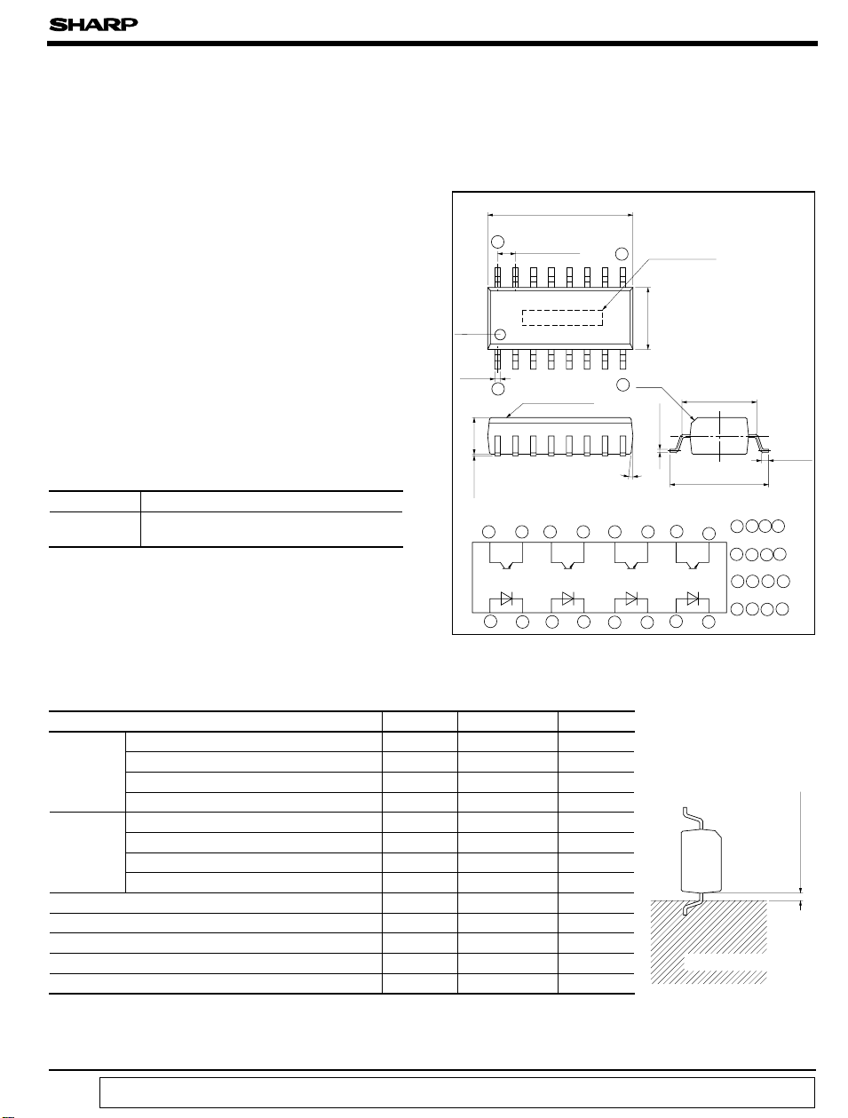
■ Package Specifications
Model No.
PC3Q66Q
Package specifications
Taping reel diameter 330mm (1 000pcs.
10
(
Unit : mm
± 0.3
5.3
+ 0.2
7.0
- 0.7
9
10
1357
Anode
2468
Cathode
11
9
Emitter
12
Collector
■ Outline Dimensions
± 0.3
10.3
16
Primary
side
mark
±0.1
0.4
± 0.2
2.6
± 0.1
0.1
)
16 1515141413 12 11
12345678
± 0.25
1.27
1
Epoxy resin
Internal connection diagram
9
8
Model No.
± 0.2
4.4
C0.4
± 0.05
0.2
6˚
)
+ 0.4
0.5
- 0.2
13
16
■ Absolute Maximum Ratings
(
Ta= 25˚C
)
Parameter Symbol Rating Unit
Forward current
*1
Input
Peak forward current
Reverse voltage V
Power dissipation
Collector-emitter voltage V
Output
Emitter-collector voltage V
Collector current I
Collector power dissipation
Total power dissipation
*2
Isolation voltage
Operating temperature T
Storage temperature
*3
Soldering temperature
*1 Pulse width<=100µs, Duty ratio : 0.001
*2 AC for 1 min., 40 to 60%RH, f= 60Hz
*3 For 10seconds
“ In the absence of confirmation by device specification sheets, SHARP takes no responsibility for any defects that occur in equipment using any of SHARP's devices, shown in catalogs,
data books, etc. Contact SHARP in order to obtain the latest version of the device specification sheets before using any SHARP's device.”
I
F
I
FM
R
P70mW
CEO
ECO
C
P
C
P
tot
V
iso
opr
T
stg
T
sol
50 mA
1A
6V
80 V
6V
50 mA
150 mW
170 mW
2.5 kV
- 30 to + 100 ˚C
- 40 to+ 125 ˚C
260 ˚C
rms
Soldering area
0.2mm or more
Page 2
PC3Q66Q
■Electro-optical Characteristics
Parameter Symbol Conditions MIN. TYP. MAX. Unit
Forward current
Input
Output
Transfer
characteristics
Fig. 1 Forward Current vs.
Ambient Temperature
)
mA
(
F
Forward current I
Reverse current
Terminal capacitance
Collector dark current
Collector-emitter breakdown voltage
Emitter-collector breakdown voltage
Collector current I
Collector-emitter saturation voltage
Isolation resistance
Floating capacitance
Response time
60
50
40
30
20
Rise time t
Fall time t
V
BV
BV
V
I
C
I
CEO
CE(sat
R
C
IF= 20mA - 1.2 1.4 V
F
VR=4V - - 10 µA
R
t
V= 0, f= 1kH
Z
- 30 250 pF
VCE= 20V, IF= 0 - - 100 nA
CEOIC
ECOIE
C
ISO
f
r
f
= 0.1mA, IF= 0 80 - - V
=10µA, IF=0 6 - - V
IF= 1mA, VCE=5V 1 - 4 mA
)
IF= 20mA, IC= 1mA - 0.1 0.2 V
DC500V 40 to 60%RH 5 x 10
V= 0, f= 1 MH
Z
VCE= 2V, IC= 2mA
= 100Ω
R
L
10
11
10
- 0.6 1.0 pF
-6-
-8-
Fig. 2 Diode Power Dissipation vs.
Ambient Temperature
)
100
mW
(
80
70
60
40
Diode power dissipation P
20
(
Ta= 25˚C
- Ω
)
µ s
µ s
0
-30100 25 5055 75 100 125
Ambient temperature Ta (˚C
)
Fig. 3 Collector Power Dissipation vs.
Ambient Temperature
200
)
mW
(
150
C
100
50
Collector power dissipation P
0
-30
0 125
25 50 75 100
Ambient temperature T
)
(˚C
a
0
-30
0 5055 100
Ambient temperature T
Fig. 4 Power Dissipation vs.
Ambient Temperature
300
250
)
mW
(
200
tot
170
150
100
Power dissipation P
50
0
- 30 0 25 50 75 100
Ambient temperature Ta (˚C
)
(˚C
a
)
Page 3

PC3Q66Q
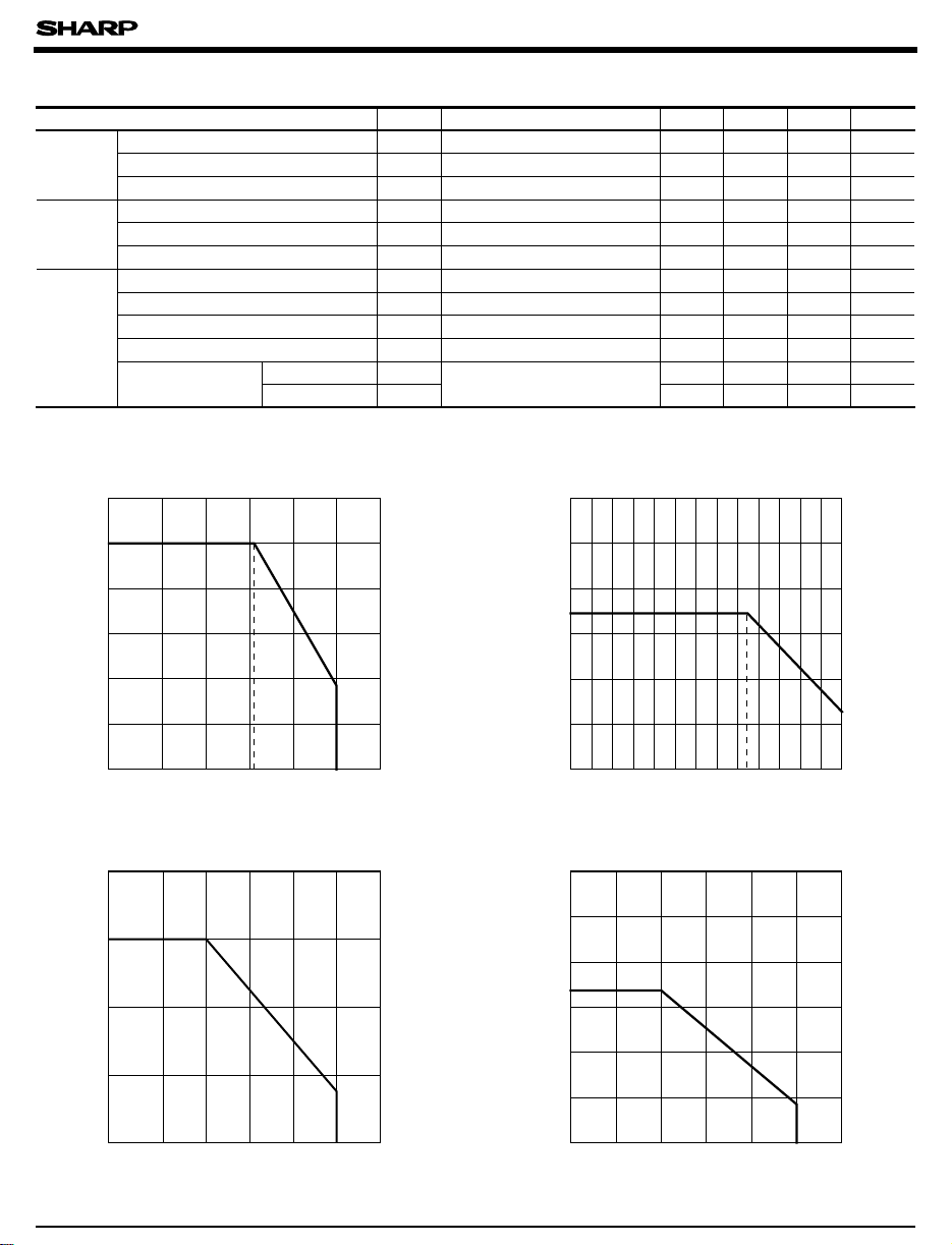
Fig. 5 Peak Forward Current vs. Duty Ratio
10000
5000
)
2000
mA
(
1000
FM
500
200
100
50
Peak forward current I
20
10
5
-3
2
5
10
5
10
-2
2
Duty ratio
Pulse width <=100µ s
Ta= 25˚C
-1
2
5
10
5
1
Fig. 7 Current Tranfer Ratio vs.
Forward Current
500
400
)
%
(
V
T
=5V
CE
= 25˚C
a
300
200
Current tranfer ratio CTR
100
0
1 10 100
Forward current IF (mA
)
Fig. 9 Relative Current Transfer Ratio vs.
Ambient Temperature
150
)
%
(
100
50
Relative current transfer ratio
0
-30
020406080100
Ambient temperature Ta (˚C
I
V
= 1mA
F
CE
)
=5V
Fig. 6 Forward Current vs.
Forward Voltage
100
)
(
mA
F
50
20
10
50˚C
75˚C
25˚C
0˚C
- 25˚C
5
Forward current I
2
1
0.0 0.5 1.0 1.5 2.0 2.5 3.0
Forward voltage V
)
(V
F
Fig. 8 Collector Current vs. Collector
-emitter Voltage
T
= 25˚C
a
)
mA
(
50
Pc (max)
I
= 30mA
F
20mA
40
C
10mA
30
20
5mA
Collector current I
10
0
0246
Collector-emitter voltage VCE (V
1mA
810
)
Fig.10 Collector-emitter Saturation Voltage vs.
Ambient Temperature
0.16
I
= 20mA
F
0.14
I
= 1mA
C
0.12
)
0.10
V
(
)
sat
(
0.08
CE
0.06
Collector-emitter saturation
0.04
voltage V
0.02
0.00
-30
020406080100
)
Ambient temperature T
(˚C
a
Page 4

PC3Q66Q
Fig.11 Collector Dark Current vs.
Ambient Temperature
-5
10
5
-6
10
)
5
A
(
-7
10
CEO
5
-8
10
5
-9
10
5
-10
Collector dark current I
10
5
-11
10
-30
Ambient temperature Ta (˚C
04080
= 20V
V
CE
1006020
)
Fig.13 Collector-emitter Saturation Voltage
vs. Forward Current
I
= 0.5mA
C
Ta= 25˚C
1mA
3mA
5mA
7mA
)
10
V
(
)
sat
(
8
CE
6
4
Fig.12 Response Time vs. Load Resistance
1000
V
=2V
CE
500
= 2mA
I
C
200
= 25˚C
T
a
100
50
)
µ s
20
(
10
5
2
Response time
1
t
r
t
d
0.5
0.2
0.1
0.01 0.1 1 10
Load resistance RL (kΩ
t
f
t
s
)
2
0
Collector-emitter saturation voltage V
02468
Forward current IF (mA
Please refer to the chapter “ Precautions for Use”
●
)
10
 Loading...