

Page 1
PC354NT
PC354NT
Mini-flat Package,
AC Input Type Photocoupler
■ Features
1. AC inputs
2. Opaque type, mini-flat package
PC354NT (1-channel
3. Subminiature type
(The volume is smaller than that of our
)
conventional DIP type by as far as 30 %.
4. Isolation voltage between input and output
PC354NT•••V
: 3 750V
iso
rms
■ Applications
1. Hybrid substrates that require high density
mounting.
2. Programmable controllers
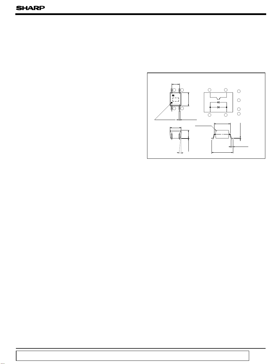
5.3
7.0
± 0.3
+ 0.2
- 0.7
34
(
Unit : mm
1 Anode/
Cathode
2 Anode/
Cathode
3 Emitter
4 Collector
± 0.05
+ 0.4
0.5
- 0.2
■ Outline Dimensions
0.4
± 0.1
Internal connection
diagram
± 0.2
4.4
12
C0.4
Input side
± 0.2
2.6
± 0.1
0.1
± 0.25
2.54
34
354
3.6
21
± 0.3
6˚
)
Primary
side mark
)
0.2
“ In the absence of confirmation by device specification sheets, SHARP takes no responsibility for any defects that occur in equipment using any of SHARP's devices, shown in catalogs,
data books, etc. Contact SHARP in order to obtain the latest version of the device specification sheets before using any SHARP's device. ”
Page 2
PC354NT
■ Absolute Maximum Ratings
Parameter
Forward current
*1
Peak forward current
Input
Power dissipation
Collector-emitter voltage V 35 V
Output
Emitter-collector voltage V 6 V
Collector current I
Collector power dissipation P
Total power dissipation 170 mW
*2
Isolation voltage V
Operating temperature - 30 to + 100 ˚C
Storage temperature - 40 to + 125 ˚C
*3
Soldering temperature 260 ˚C
*1 Pulse width<=100µs, Duty ratio : 0.001
*2 40 to 60%RH, AC for 1 minute
*3 For 10 senconds
Classification of current transfer ratio (CTR
Model No. Rank mark
PC354N1T
PC354NT
❈ Conditions : IF= ± 1mA, VCE= 5V, Ta= 25˚C
A or No mark
CTR (%
A 50 to 150
20 to 400
)
)
■ Electro-optical Characteristics
Parameter Symbol Conditions MIN. TYP. MAX. Unit
Input
Output
Transfercharacteristics
Forward voltage
Terminal capacitance
Collector dark current
Collector-emitter breakdown voltage
Emitter-collector breakdown voltage
Current transfer ratio
Collector-emitter saturation voltage
Isolation resistance
Floating capacitance
Response time
Rise time
Fall time
(
Ta= 25˚C
Symbol Rating Unit
I
F
I
FM
P
CEO
ECO
C
C
P
tot
iso
T
opr
T
stg
T
sol
V
FIF
C
t
I
CEO
BV
CEOIC
BV
ECOIE
CTR I
V
CE(sat
R
ISO
C
f
t
r
t
f
±50 mA
±1 A
70 mW
50 mA
150 mW
3 750
V
= ± 20mA
V= 0, f= 1kHz
V
= 20V, I
CE F
=0 - - A
= 0.1mA, IF=0 35 - V
=10µA, IF=0 6 - - V
= ± 1mA, VCE= 5V 20 - 400 %
F
)
= ± 20mA, I
I
F
= 1mA
C
DC500V, 40 to 60%RH
V= 0, f= 1MHz - 0.6 1.0 pF
VCE= 2V, IC= 2mA
= 100Ω
R
L
)
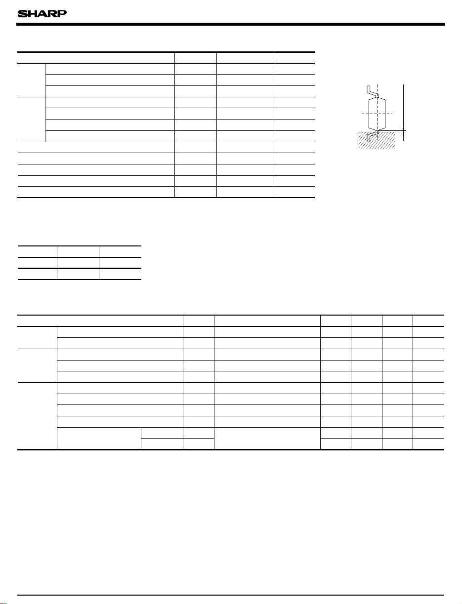
Soldering area
0.2mm or more
rms
(
Ta= 25˚C
- 1.2 1.4 V
- 30 250 pF
-7
10
-
- 0.1 0.2 V
5x101010
11
- Ω
-418µs
-318µs
)
Page 3

PC354NT
Fig. 1 Forward Current vs. Ambient
Temperature
70
60
)
50
mA
(
F
40
30
20
Forward current I
10
0
0 25 50 75 100 125
-30
Ambient temperature Ta (˚C
)
Fig. 3 Collector Power Dissipation vs.
Ambient Temperature
200
)
mW
(
150
C
100
50
Collector power dissipation P
Fig. 2 Diode Power Dissipation vs.
Ambient Temperature
)
100
mW
(
80
70
60
40
Diode power dissipation P
20
0
-30
0 50 55 100
Ambient temperature T
(˚C
a
Fig. 4 Total Power Dissipation vs.
Ambient Temperature
300
)
250
mW
(
tot
200
170
150
100
50
Total power dissipation P
)
0
0 25 50 75 100 125
-30 -30
Ambient temperature T
a
(˚C
)
0
0 50 10025
Ambient temperature T
a
(˚C
)
Fig. 5 Peak Forward Current vs. Duty Ratio Fig. 6 Forward Current vs. Forward Voltage
10000
5000
)
2000
mA
(
1000
FM
500
200
100
50
Peak forward current I
20
10
5
-3
5252525
10
10
Duty ratio
-2
Pulse width <=100 µs
Ta= 25˚C
10
-1
1
500
200
)
100
mA
(
50
F
20
10
5
Forward current I
1
020.5 1.0 1.5 2.0 2.5 3.0 3.5
= 75˚C
T
a
50˚C
Forward voltage VF (V
25˚C
0˚C
- 25˚C
)
Page 4

PC354NT
Fig. 7 Current Transfer Ratio vs.
Forward Current
500
)
%
400
(
300
V
CE =
Ta= 25˚C
5V
Fig. 8 Collector Current vs. Collector-
emitter Voltage
)
(
mA
C
50
40
= 30mA
I
F
(
30
20mA
C
P
MAX.
=
Ta
25˚C
)
10mA
200
Current transfer ratio CTR
100
20
Collector current I
10
5mA
1mA
0
0.1 1 10 100
Forward current I
(mA
F
)
0
010123456789
Collector-emitter voltage VCE (V
)
Fig. 9 Relative Current Transfer Ratio vs. Fig.10 Collector-emitter Saturation Voltage
Ambient Temperature
150
)
%
(
100
50
Relative current transfer ratio
0
30 100020
Ambient temperature Ta (˚C
I
= 5mA
F
V
=5V
CE
40 8060 60 8040
)
vs. Ambient Temperature
0.16
0.14
0.12
0.10
0.08
)
0.06
V
(
)
sat
(
0.04
CE
Collector-emitter saturation voltage
V
0.02
0
200 100-- 30
Ambient temperature Ta (˚C
I
= 20mA
F
= 1mA
I
C
)
Fig.11 Collector Dark Current vs. Fig.12 Response Time vs. Load Resistance
Ambient Temperature
-5
10
5
-6
)
10
A
(
5
-7
CEO
10
5
-8
10
5
-9
10
5
Collector dark current I
-10
10
5
-11
10
-30
Ambient temperature Ta (˚C
V
= 20V
CE
100
806040200
)
500
=2V
V
CE
I
= 2mA
C
200
T
= 25˚C
a
)
100
µs
(
50
20
t
r
t
f
10
5
Response time
t
2
1
d
t
s
0.5
0.2
0.1
0.01
0.1 1 10
Load resistance RL (kΩ
)
50
Page 5

Input
Test Circuit For Response Time
V
CC
Output
Input
Output
R
R
D
L
10%
Fig.13 Collector-emitter Saturation
Voltage vs. Forward Current
5.6
4.2
2.8
= 0.5mA
I
C
Ta= 25˚C
1mA
3mA
5mA
7mA
PC354NT
90%
t
d
t
s
t
t
r
f
■ Temperature Profile of Soldering Reflow
30 seconds
230˚C
200˚C
180˚C
1 minute
25˚C
2 minutes 1.5 minutes 1 minute
Please refer to the chapter “ Precautions for Use ”.
●
)
V
(
1.4
)
sat
(
CE
Collector-emitter saturation voltage
V
0
(1)
One time soldering reflow is recommended
2345678910
01
Forward current I
F
(mA
)
within the condition of temperature and
time profile shown below.
(2)
When using another soldering method such
as infrared ray lamp, the temperature may
rise partially in the mold of the device.
Keep the temperature on the package of
the device within the condition of above
(1)
.
 Loading...