

Page 1
PC353T
PC353T
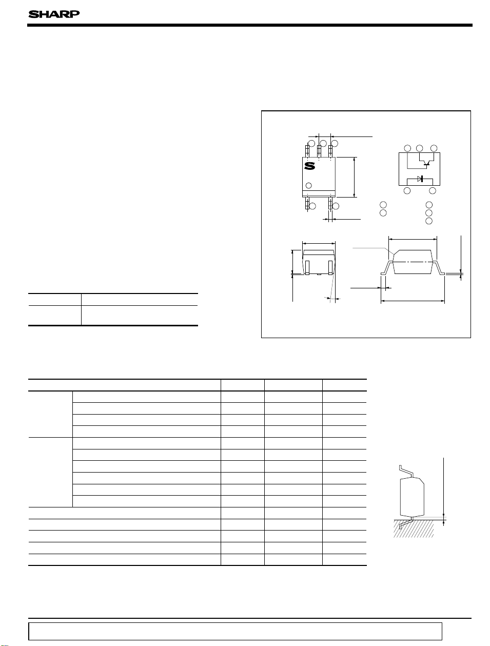
Mini-flat Package
Photocoupler with Base
Terminal
■ Features
1. With base terminal
2. Applicable to infrared ray reflow
(230˚C, MAX. 30 seconds
)
3. High isolation voltage
(V
: 3 750V
iso rms
)
4. Recognized by UL (No. E64380)
5. Mini-flat package
■ Applications
1. Hybrid substrates that reguire high denity
mounting
2. Programmable controllers
■ Package Specifications
Model No. Taping specifications
PC353T
Taping reel diameter
178mm (750pcs.
)
■ Absolute Maximum Ratings
Parameter Symbol Rating Unit
Forward current
*1
Input
Output
Peak forward current
Reverse voltage V
Power dissipation
Collector-emitter voltage V
Emitter-collector voltage V
Collector-base voltage V
Emitter-base voltage V
Collector current I
Collector power dissipation
Total power dissipation
*2
Isolation voltage
Operating temperature T
Storage temperature T
*3
Soldering temperature
■ Outline Dimensions
± 0.25
1.27
654
353
13
3.6
± 0.2
2.6
± 0.1
0.1
(
I
F
I
FM
R
P70mW
CEO
ECO
CBO
EBO
C
P
C
P
tot
V
iso
opr
stg
T
sol
50 mA
1A
6V
80 V
6V
80 V
6V
50 mA
150 mW
170 mW
3.75 kV
- 30 to + 100 ˚C
- 40 to + 125 ˚C
260 ˚C
± 0.2
4.4
± 0.1
0.4
± 0.3
6˚
Ta= 25˚C
rms
C0.4
(
Input side
+ 0.4
0.5
- 0.2
)
(
Internal connection
diagram
65 4
13
1 Anode
3 Cathode
± 0.3
5.3
)
+ 0.2
7.0
- 0.7
Soldering area
Unit : mm
4 Emitter
5 Collector
6 Base
0.2mm or more
)
± 0.05
0.2
*1 Pulse width <=100µs, Duty ratio : 0.001
*2 AC for 1 min., 40 to 60%RH, f= 60H
*3 For 10 seconds
“ In the absence of confirmation by device specification sheets, SHARP takes no responsibility for any defects that occur in equipment using any of SHARP's devices, shown in catalogs,
data books, etc. Contact SHARP in order to obtain the latest version of the device specification sheets before using any SHARP's device. ”
z
Page 2
PC353T
■ Electro-optical Characteristics
Parameter Symbol Conditions MIN. TYP. MAX. Unit
Forward voltage V
Input
Output
Transfer
characteristics
Reverse current I
Terminal capacitance C
Collector dark current
Collector-emitter
breakdown voltage
Emitter-collector I
breakdown voltage
Collector-base
breakdown voltage
Collector current I
Collector-emitter
saturation voltage
Isolation resistance
Floating capacitance C
Response time
Rise time t
Fall time t
V
BV
BV
BV
I
CEO
CE(sat
R
(
Ta= 25˚C
F
R
t
IF= 20mA - 1.2 1.4 V
VR=4V - - 10 µA
V= 0, f = 1kHz
- 30 250 pF
)
VCE= 20V, IF= 0 - - 100 nA
= 0.1mA
I
CEO
ECO
CBO
C
)
ISO
f
r
f
C
=0
I
F
=10µA
E
=0
I
F
= 0.1mA
I
C
=0
I
F
IF= 5mA
=5V
V
CE
= 20mA
I
F
= 1mA
I
C
DC500V
40 to 60%RH
V= 0, f = 1MH
V
= 2V, IC= 2mA
CE
= 100 Ω
R
L
Z
80 - - V
6--V
80 - - V
2.5 - 30 mA
- 0.1 0.2 V
10
11
5x10
10
- Ω
- 0.6 1.0 pF
-418µs
-318µs
Fig. 1 Forward Current vs.
Ambient Temperature
50
)
40
mA
(
F
30
20
Forward current I
10
0
0 25 1007555
-30
Ambient temperature T
Fig. 2 Diode Power Dissipation vs.
Ambient Temperature
100
)
80
mW
(
70
60
40
20
Diode power dissipation P
0
-30
(˚C)
a
Ambient temperature T
55 75 100250
(˚C)
a
Page 3

PC353T
Fig. 3 Collector Power Dissipation vs.
Ambient Temperature
)
200
mW
(
150
100
50
Collector power dissipation Pc
0
-30
0 25 1007550
Ambient temperature Ta (˚C
)
Fig. 5 Peak Forward Current vs. Duty Ratio
10000
)
mA
(
FM
1000
100
Peak forward current I
Pulse width <=100µ s
Ta= 25˚C
Fig. 4 Total Power Dissipation vs.
Ambient Temperature
)
200
mW
(
tot
170
150
100
50
Total power dissipation P
0
-30
50 75 100250
Ambient temperature T
a
(˚C
)
Fig. 6 Forward Current vs. Forward Voltage
500
200
)
100
mA
(
F
50
20
10
Forward current I
Ta= 75˚C
50˚C
5
25˚C
0˚C
- 25˚C
10
10
-3
Duty ratio
-2
10
Forward Current
400
)
%
(
200
Current transfer ratio CTR
0
0 0.5 1.0 5.0 10 50 100
Forward current IF (mA
-1
10
RBE=
= 500kΩ
R
BE
RBE= 100kΩ
)
2
1
1
0 0.5 1.0 1.5 2.0 2.5 3.0
Forward voltage VF (V
)
Fig. 8 Collector Current vs.Fig. 7 Current Transfer Ratio vs.
Collector-emitter Voltage
50
I
= 30mA
)
40
mA
(
C
30
20
Collector current I
10
0
0
Collector-emitter voltage V
I
I
F
I
F
= 20mA
F
I
F
= 5mA
= 1mA
F
= 10mA
105
)
(V
CE
Page 4

PC353T
Fig. 9 Relative Current Transfer Ratio vs.
Ambient Temperature
150
)
%
(
100
50
Relative current transfer ratio
0
- 30 0 40 60 80 100
20
Ambient temperature T
I
F
VCE=5V
(˚C
a
= 5mA
)
Fig.11 Collector Dark Current vs.
Ambient Temperature
-5
10
5
-6
10
)
A
5
(
-7
CEO
10
5
-8
10
5
-9
10
5
Collector dark current I
-10
10
5
-11
10
- 30 0 20 40 60 100
Ambient temperature T
a
V
(˚C
CE
= 20V
80
)
Fig.13 Collector-emitter Saturation Voltage vs.
Forward Current
4.8
)
V
(
)
sat
(
3.6
CE
I
C
1mA
3mA
5mA
7mA
2.4
Ta= 25˚C
= 0.5mA
Fig.10 Collector-emitter Saturation Voltage vs.
Ambient Temperature
0.16
0.14
I
F
I
C
= 20mA
= 1mA
0.12
0.10
0.08
)
V
(
0.06
)
SAT
(
0.04
CE
Collector-emitter saturation voltage
V
0.02
0
-30
0 20406080100
Ambient temperature T
)
(˚C
a
Fig.12 Response Time vs. Load Resistance
500
V
=2A
CE
IC= 2mA
200
T
= 25˚C
a
100
)
50
µs
(
20
10
5
Response Time
2
1
0.5
0.2
0.1
0.01 0.1 1 10
t
f
t
r
t
d
t
s
Load resistance R
(kΩ
L
)
1.2
0
Collector-emitter saturation voltage V
0
3 6 9 12 15
Foward current IF (mA
Please refer to the chapter “Precautions for Use.”
●
)
 Loading...