

Page 1
TECH. CORP.
SPECIFICATIONS
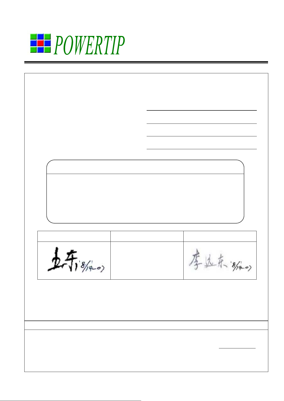
CUSTOMER
SAMPLE CODE (Ver.)
MASS PRODUCTION CODE (Ver.)
DRAWING NO. (Ver.)
:
:
PC1602LRS-HWB-H-Q (VER.A)
:
PC-95005
:
Customer Approved
Approved QC Confirmed Designer
Date:
■
□
Headquarters:
Approval For Specifications Only.
* This specification is subject to change without notice.
Please contact Powertip or it’s representative before designing your product based on this specification.
Approval For Specifications and Sample.
POWERTIP TECH. CORP.
No.8, 6th Road, Taichung Industrial Park,
Taichung, Taiwan
台中市 407 工業區六路 8號
TEL: 886-4-2355-8168
FAX: 886-4-2355-8166
E-mail: sales@powertip.com.tw
Http://www.powertip.com.tw
NO.PT-A-005-7
Page 2
o
RECORDS OF REVISION
Date Ver. Description Page Design by
2006/7/21
2007/8/14
0
PC1602LRS-HWB-H-Q is the ROHS compliant part number based
Powertip's standard PC1602LRS-HWB-H
Update Timing Characteristics and Display Command
A
12,14
Total:24 Page
PC1602LRS-HWB-H-Q Rev.A (DK) Page2
Page 3

Contents
1. SPECIFICATIONS
1.1 Features
1.2 Mechanical Specifications
1.3 Absolute Maximum Ratings
1.4 DC Electrical Characteristics
1.5 Optical Characteristics
1.6 Backlight Characteristics
2. MODULE STRUCTURE
2.1 Counter Drawing
2.2 Interface Pin Description
2.3 Timing Characteristics
2.4 Display Command
2.5 Character Pattern
3. QUALITY ASSURANCE SYSTEM
3.1 Quality Assurance Flow Chart
3.2 Inspection Specification
4. RELIABILITY TEST
4.1 Reliability Test Condition
5. PRECAUTION RELATING PRODUCT HANDLING
5.1 Safety
5.2 Handling
5.3 Storage
5.4 Terms of Warranty
6. PACKING Specification
Note:For detailed information please refer to IC data sheet: ST7066U, ST7065C
PC1602LRS-HWB-H-Q Rev.A (DK) Page3
Page 4
1. SPECIFICATIONS
1.1 Features
Item Standard Value
Display Type
LCD Type STN Gray Transflective Positive Extended Temp.
Driver Condition
Viewing Direction 6 O’clock
Backlight Yellow-Green LED B/L
Weight 34.0g
Interface
ROHS
1.2 Mechanical Specifications
Item Standard Value Unit
Outline Dimension 85.0 (L) * 36.0 (w) * 14.5 (H)(Max) mm
Viewing Area 66.0 (L) *16.0 (w) mm
16 * 2 Characters
LCD Module 1/16 Duty,1/4 Bias
-
THIS PRODUCT CONFORMS THE ROHS OF PTC
Detail information please refer web side :
http://www.powertip.com.tw/news/LatestNews.asp
Active Area 56.21 (L) * 11.5 (w) mm
Dot Size 0.56(L) * 0.66 (w) mm
Dot Pitch 0.60 (L) * 0.70 (w) mm
Note:For detailed information please refer to LCM drawing
1.3 Absolute Maximum Ratings
Item Symbol Condition Min. Max. Unit
Power Supply Voltage VDD
LCD Driver Supply Voltage V
Input Voltage VIN -0.3 VDD+0.3 V
Operating Temperature TOP -20 70
Storage Temperature TST
Storage Humidity HD
PC1602LRS-HWB-H-Q Rev.A (DK) Page4
LCD
Excluded B/L
-
-
Ta<40 ℃
-0.3 7.0 V
VDD-10.0 VDD+0.3 V
℃
-30 80
℃
- 90 %RH
Page 5
1.4 DC Electrical Characteristics
Item Symbol Condition Min. Typ. Max. Unit
V
= 5.0 V ± 0.5V,V
DD
= 0V,Ta = 25℃
SS
Logic Supply Voltage VDD
“H” Input Voltage VIH
“L” Input Voltage VIL
“H” Output Voltage VOH
“L” Output Voltage VOL
Supply Current IDD V
LCM Driver Voltage VOP
Note: *1. THE VOP TEST POINT IS VDD - VO.
1.5 Optical Characteristics
LCD Panel:1/16 Duty,1/4 Bias,V
Item Symbol Conditions Min. Typ. Max. Reference
-
-
-
l
=-0.1mA
OH
lOL=0.1mA
= 5.0 V - 1.5 3.0 mA
DD
4.5 5.0 5.5 V
0.7 VDD - VDD V
-0.3 - 0.6 V
3.9 - V
V
DD
- - 0.4 V
-20℃ - - -
25 *℃ 6.0 6.2 6.4
V
70℃ - - -
= 6.7 V,Ta = 2 5℃
LCD
View Angle θ
Contrast Ratio C
Response Time(rise) tr
Response Time(fall) tf
C>2.0, ∅ = 0°
θ = 5°, ∅ = 0°
θ = 5°, ∅ = 0°
θ = 5°, ∅ = 0°
0° - 40° Notes 1 & 2
5 7 - Note 3
- 150 ms - Note 4
- 300 ms - Note 4
PC1602LRS-HWB-H-Q Rev.A (DK) Page5
Page 6
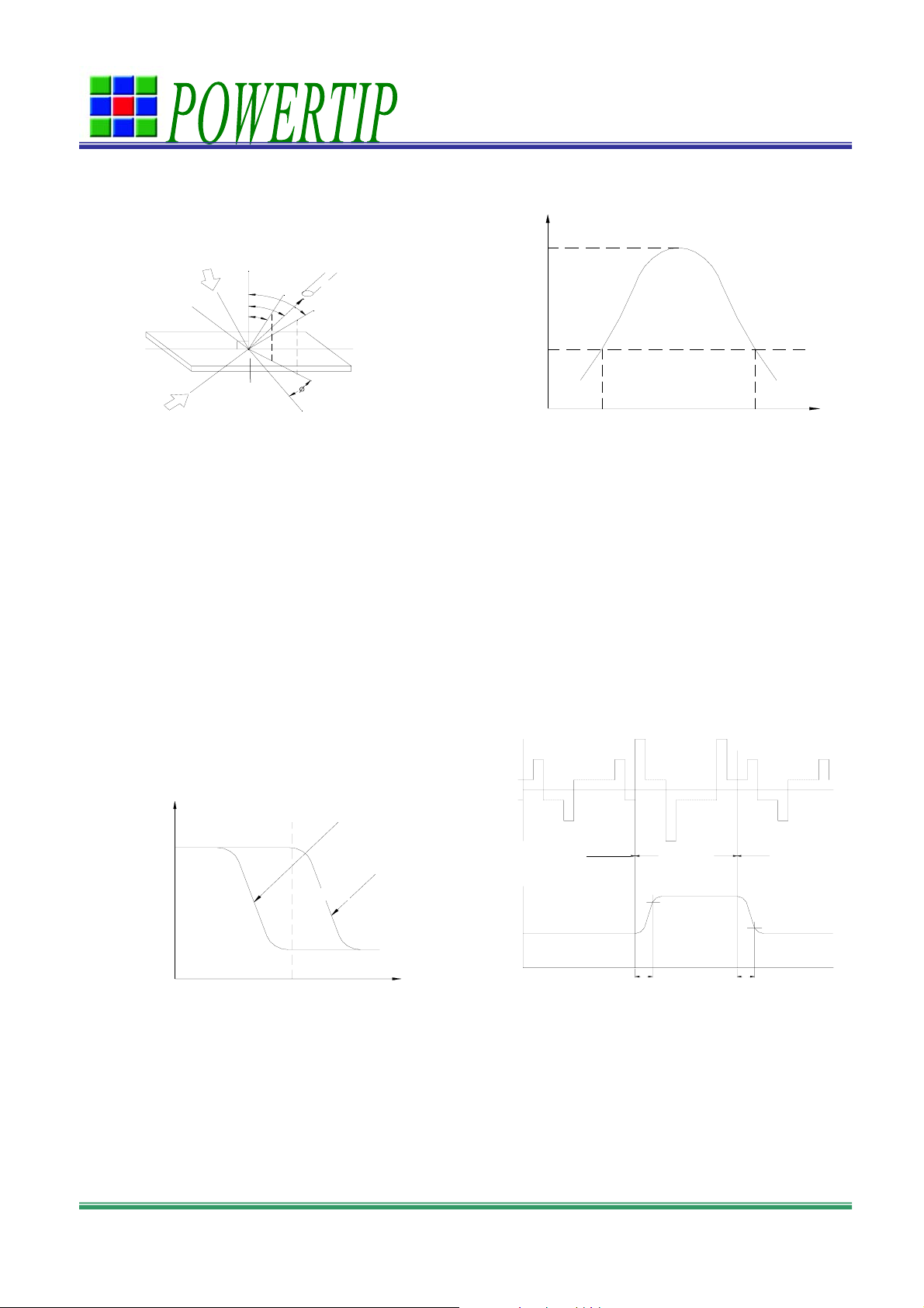
Note 1: Definition of angles θ and ∅ Note 2: Definition of viewing angles θ1 and θ2
Light (when reflected) z (θ=0°)
Sensor
Cmax.
θ
Y’(∅=180°)
LCD panel
X’
Z’
θ1 θ2
Light (when transmitted )
∅
Y(∅=0°)
X(∅=90°)
Contrast
2.0
viewing angle θ (∅ fixed)
Note : Optimum viewing angle with the
°
naked eye and viewing angle θ at
Cmax. Above are not always the same
Note 3: Definition of contrast C Note 4: Definition of response time
Brightness (reflection) of unselected dot (B2)
C = ⎯⎯⎯⎯⎯⎯⎯⎯⎯⎯⎯⎯⎯⎯⎯⎯⎯⎯
Brightness (reflection) of selected dot (B1)
VLCD
Brightness (reflection) of
selected dot
0
-VLCD
Non-selected state
Contrast
Selected state
90%
tr tf
Non-selected state
10%
(%)
Brightness
(reflection) of
unselected dot
Brightness
(reflection)
B2
B1
0 Note: Measured with a transmissive LCD
operating voltage (v) panel which is displayed 1 cm
2
V
t
: Operating voltage f
LCD
: Response time (rise) tf : Response time (fall)
r
: Frame frequency
FRM
Time
PC1602LRS-HWB-H-Q Rev.A (DK) Page6
Page 7

1.6 Backlight Characteristics
LCD Module with LED Backlight
Maximum Ratings
Item Symbol Conditions Min. Max. Unit
Forward Current IF Ta =25℃ - 300 mA
Reverse Voltage VR Ta =25℃ - 8 V
Power Dissipation PO Ta =25℃ - 1.38 W
E
lectrical / Optical Characteristics
Ta =25℃
Item Symbol Conditions Min. Typ. Max. Unit
Forward Voltage VF IF= 120mA - 4.2 4.6 V
Reverse Current IR VR= 8 V - - 0.2 mA
Average Brightness
IV IF=120mA 220 290 - cd/m2
(without LCD)
Wavelength Hue IF=120mA 569 - 576 nm
Color Yellow-Green
PC1602LRS-HWB-H-Q Rev.A (DK) Page7
Page 8
2. MODULE STRUCTURE
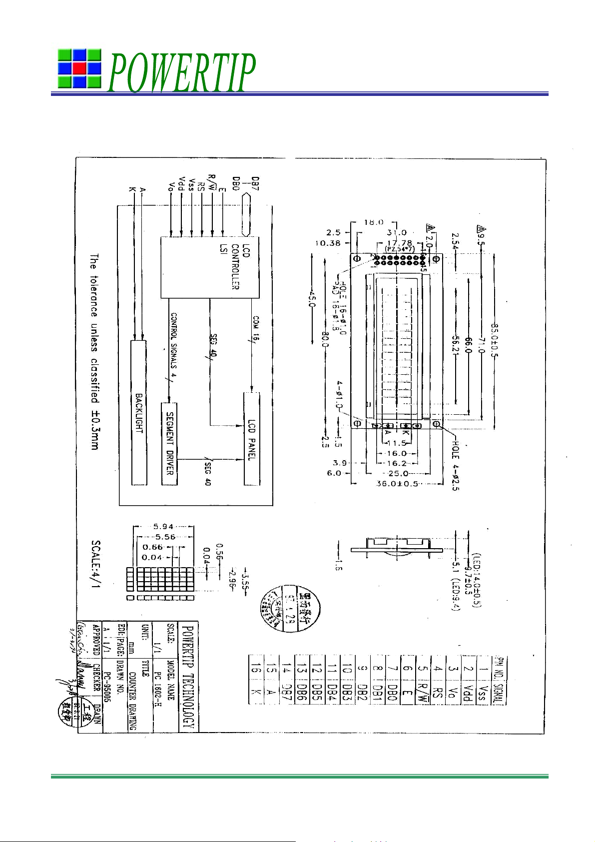
2.1 Counter Drawing
PC1602LRS-HWB-H-Q Rev.A (DK) Page8
Page 9

2.2 Interface Pin Description
Pin No. Symbol Function
1 Vss Signal ground (GND)
2 VDD Power Supply for logic (VDD> Vss)
3 VO Operating Voltage for LCD (variable)
Register selection input
4 RS
5
R/W
6 E Start enable signal to read or write the data
7-10 DB0 ~ DB3
11~14 DB4~DB7
15 A Power supply for LED backlight (+)
16 K Power supply for LED backlight (-)
High = Data register
Low = Instruction register (for write)
Busy flag address counter (for read)
Read/Write signal input is used to select the read/write
mode. High = Read mode, Low = Write mode
Four low order bi-directional three-state data bus lines.
Used
for data transfer between the MPU and the LCD module.
These four are not used during 4-bit operation.
Four high order bi-directional three-state data bus lines.
Used for data transfer between the MPU and the LCD
module.
DB7 can be used as a busy flag.
Contrast Adjust
10~20KΩ
PC1602LRS-HWB-H-Q Rev.A (DK) Page9
VDD
V
O
V
SS
2
LCD MODULE
3
1
15
16
4.2V
Page 10

2.3 Timing Characteristics
• Writing data from MPU to ST7066U
RS
R/W
E
DB0-DB7
VIH1
VIL1
TAS
TR
TPW
TDSW
Valid data
TAH
TAH
TH
z Reading data from ST7066U to MPU
RS
VIH1
VIL1
TAS
R/W
TR
E
TDDR
DB0-DB7
TPW
C
T
TAH
TAH
Valid data
TH
PC1602LRS-HWB-H-Q Rev.A (DK) Page10
TC
Page 11

• Write Mode (Writing data from MPU to ST7066U)
(VDD= +5V+10%,Ta=25°C)
Symbol Characteristics Test Condition Min. Typ. Max. Unit
TC Enable Cycle Time Pin E 1200 - - ns
TPW Enable Pulse Width Pin E 140 - - ns
TR , TF Enable Rise / Fall Time Pin E - - 25 ns
TAS Address Setup Time Pins: RS , RW,E 0 - - ns
TAH Address Hold Time Pins :RS,RW,E 10 - - ns
T
Data Setup Time Pins:DB0~DB7 40 - - ns
DSW
TH Data Hold Time Pins:DB0~DB7 10 - - ns
• Read Mode (Reading data from ST7066U to MPU)
(VDD = +5V+10%,Ta=25°C)
Symbol Characteristics Test Condition Min. Typ. Max. Unit
TC Enable Cycle Time Pin E 1200 - - ns
TPW Enable Pulse Width Pin E 140 - - ns
TR , TF Enable Rise / Fall Time Pin E - - 25 ns
TAS Address Setup Time Pins: RS , RW,E 0 - - ns
TAH Address Hold Time Pins :RS,RW,E 10 - - ns
T
Data Setup Time Pins:DB0~DB7 - - 100 ns
DDR
TH Data Hold Time Pins:DB0~DB7 10 - - ns
PC1602LRS-HWB-H-Q Rev.A (DK) Page11
Page 12

For 4-bit interface date, only four bus lines (DB4 to DB7) are used for transfer.
Example of busy flag check timing sequence
For 8-bit interface date, all eight bus lines (DB0 to DB7) are used .
Example of busy flag check timing sequence
PC1602LRS-HWB-H-Q Rev.A (DK) Page12
Page 13

2.4 Display Command
Description
Instructions
Clear
Display
Return
Home
Entry Mode
Set
Display
Instruction Code Description
DB 7 DB 6DB 5 DB 4 DB 3 DB2DB1 DB
RS R/W
0 0 0 0 0 0 0 0 0 1
0 0 0 0 0 0 0 0 1 ×
0 0 0 0 0 0 0 1 I/D S
Tim e
(270KHz)
0
Write "20H" to DDRAM. and set
DDRAM address to "00H" from
1.52ms
AC.
Set DDRAM address to "00H"
from AC and return cursor to it's
original position if shifted.
1.52ms
The contents of DDRAM are not
changed.
Sets cursor move direction and
specifies display shift. These
37µs
operations are performed during
data write and read .
D=1 : entire display on
ON/OFF 0 0 0 0 0 0 1 D C B
C=1 : cursor on
B=1 : cursor position on
Cursor or
Set cursor moving and display
S/C R/
Display
0 0 0 0 0 1
××
shift control bit, and the direction,
L
Shift
without changing of DDRAM data.
DL: interface data is 8/4 bits
Function
0 0 0 0 1 DL N F × ×
NL: number of line is 2/1
Set
F: font size is 5×11/5×8
A
Set CGRAM
0 0 0 1
Address
Set DDRAM
0 0 1 AC
Address
PC1602LRS-HWB-H-Q Rev.A (DK) Page13
AC 5 AC
AC 5 AC
6
4
4
C
3
A
C
3
C
2
A
C
2
A
AC
1
AC
1
A
Set CGRAM address in address
C
counter.
0
A
Set DDRAM address in address
C
counter.
0
37µs
37µs
37µs
37µs
37µs
Page 14

Read Busy
Flag and
Address
0 1
B
F
A
AC 5 AC
C
6
4
A
C
3
A
C
Whether during internal operation
A
AC
1
2
or not can be known by reading
C
BF. The contents of address
0
0µs
counter can also be read.
Write Data
1 0
to RAM
Read Data
1 1
from RAM
D7 D
D7 D
D5 D4
6
D5 D4
6
D3 D
D3 D
D0Write data into internal RAM
D1
2
(DDRAM/CGRAM).
37µs
D0Read data from internal RAM
D1
2
(DDRAM/CGRAM).
37µs
Note:
Be sure the ST7066U is not in the busy state (BF=0) before sending an instruction from the MPU to the
ST7066.
If an instruction is sent without checking the busy flag , the time between the first instruction and next
instruction will take much longer than the instruction time itself.
Before checking BF, be sure to wait at least 80us.. Do not keep “E” always “High” for checking BF.
Refer to Instruction Table for the list of each instruction execution time .
PC1602LRS-HWB-H-Q Rev.A (DK) Page14
Page 15

2.5 Character Pattern
PC1602LRS-HWB-H-Q Rev.A (DK) Page15
Page 16

3. QUALITY ASSURANCE SYSTEM
3.1 Quality Assurance Flow Chart
Item Customer Sales R&D Q.A Manufacturing
Info. Survey
Marketing
&
Design
Sample
Approval
Request Inquiry Design evaluation
Quote
Contract
Design check
Sample test
Product
control
Purchase
Inventory
control
Pilot Run
&
Mass
Product
Ship Out
Sample approval
Pilot run & Reliability test
Specification preparation
Mass production
Inspection
Shipment
Ship out
PC1602LRS-HWB-H-Q Rev.A (DK) Page16
Page 17

Info. Claim
Failure analysis
Sales
Service
Q.A
Activity
Analysis report
Corrective action
Tracking
1. ISO 9001 Maintenance Activities 2. Process improvement proposal
3. Equipment calibration 4. Education And Training Activities
5. Standardization Management
PC1602LRS-HWB-H-Q Rev.A (DK) Page17
Page 18

3.2 Inspection Specification
◆Inspection Standard : MIL-STD-105E Table Normal Inspection Single Sampling Level Ⅱ .
◆Equipment : Gauge、MIL-STD、Powertip Tester、Sample
◆Defect Level : Major Defect AQL 0.4; Minor Defect AQL 1.5 .
◆OUT Going Defect Level : Sampling .
◆Manner of appearance test :
(1). The test be under 40W×2 fluorescent light ’ and distance of view must be at 30 cm.
(2). The test direction is base on about around 45° of vertical line. (Fig. 1)
(3). Definition of area . (Fig. 2)
◆ Specification:
NO Item Criterion level
1.1 The part number is inconsistent with work order of
Major
01
Product condition
Production.
1.2 Mixed production types. Major
1.3 Assembled in inverse direction. Major
02 Quantity 2.1 The quantity is inconsistent with work order of production. Major
3.1 Product dimension and structure must conform to
03 Outline dimension
Major
Structure diagram.
04
Electrical Testing
4.1 Missing line character、dot and icon.
4.2 No function or no display. Major
4.3 Output data is error. Major
Major
4.4 LCD viewing angle defect. Major
4.5 Current consumption exceeds product specifications. Major
Black or white
5.1 Round type:
5.1.1 display only :
dot、scratch、
05
contamination
‧White and black spots on display ≦ 0.25mm, no more
Minor
than Four white or black spots present.
Round type
‧Densely spaced : NO more than two spots or lines within
3mm
◆Specification :
PC1602LRS-HWB-H-Q Rev.A (DK) Page18
Page 19

NO Item Criterion level
05
Black or white
dot、scratch、
contamination
Round type
Φ=(x+y)/2
5.1.2 Nom-display :
Dimension (diameter : Φ)
Φ≦0.10mm
0.10mm<Φ≦0.20mm
0.20mm<Φ≦0.25mm
5.1.3 Line type:
---
L≦3.0mm 0.03mm<
L≦2.5mm 0.05mm<
Total 4
Dimension (diameter : Φ)
Length width A area B area
w≦0.03mm
Φ≦0.05mm
Φ≦0.075mm
Acceptance(Q’ty)
Accept no dense
3
2
Acceptance (Q’ty)
Accept no
dense
4
Don’t
count
Don’t
count
Don’t
count
Minor
06
07
Polarizer
Bubble
The crack of
glass
Acceptance(Q’ty)
Dimension (diameter : Φ)
● Glass Crack:
7.1 Crack on the circuit of electrode terminal :
Φ≦0.20mm
0.20mm<Φ≦0.50mm
0.50mm<Φ≦1.00mm
Φ>1.00mm
Total quantity 4 Don’t count
X Y Z
A area B area
Accept no dense Don’t count
3 Don’t count
2 Don’t count
0 Don’t count
Minor
Minor
Front
PC1602LRS-HWB-H-Q Rev.A (DK) Page19
Back Neglect
X≦1/5 a Y≦ 1/2 D Z≦ t
Page 20

◆Specification :
NO Item Criterion Level
The crack of
X: The length of
Y: The width of
07
Z: The thickness
of crack
glass
Crack
crack
● Glass Crack:
7.2 General glass crack and corner edge:
7.2.1
X Y Z
Neglect Out A area Neglect
X Y Z
Neglect Out A area Neglect
Minor
D: terminal
length
7.3 Glass remain:
T: The thickness
of glass
A : The length of
glass
X Y
Neglect
PC1602LRS-HWB-H-Q Rev.A (DK) Page20
Minor
≦ 1/3 d
Page 21

◆Specification :
NO Item Criterion Level
The crack of glass
X: The length of
Y: The width of
07
Crack
crack
7.4 Corner crack and medial crack:
Minor
Z: The thickness
of crack
D: terminal length
T: The thickness
A : The length of
08
Backlight
elements
09
General
appearance
of glass
glass
X Y Z
≦1/5a
Crack can’t enter viewing area
≦1/2t
Crack can’t exceed the half of
≦1/5a
width of SP width of SP
1/2t<Z≦2t
8.1 Backlight can’t work normally. Major
8.2 Backlight doesn’t light or color is wrong. Major
8.3 Illumination source flickers when lit. Major
9.1 pin type must match type in specification sheet Major
9.2 No short circuits in components on PCB or FPC Major
9.3Product packaging must the same as specified on
packaging specification sheet.
9.4 The folding and peeled off in polarizer are not
acceptable
Major
Major
9.5 The PCB or FPC between B/L assembled distance
(PCB or FPC) is ≦1.5mm
PC1602LRS-HWB-H-Q Rev.A (DK) Page21
Major
Page 22

4. RELIABILITY TEST
4.1 Reliability T est Condition
NO. TEST ITEM TEST CONDITION
1 High Temperature Storage Test
2 Low Temperature Storage Test
3
4
5
High Humidity Storage
Vibration Test
ESD Test
Keep in 80 ±2℃ 96 hrs
Surrounding temperature, then storage at normal condition 4hrs
Keep in -30 ±2℃ 96 hrs
Surrounding temperature, then storage at normal condition 4hrs
Keep in +60℃/90%RH duration for 96 hrs
Surrounding temperature, then storage at normal condition 4hrs
(Excluding the polarizer)Or
Keep in +40℃/90%RH duration for 96 hrs
Surrounding temperature, then storage at normal condition 4hrs
1. Sine wave 10~55HZ frequency (1 min)
2. The amplitude of vibration :1.5 mm
3. Each direction (XYZ) duration for 2 Hrs
Air Discharge:
Apply 6 KV with 5 times
Discharge foreach polarity +/-
1. Temperature ambinace:15℃~35℃
2. Humidity relative:30%~60%
3. Energy Storage Capacitance(Cs+Cd):150pF±10%
4. Discharge Resistance(Rd):330Ω±10%
5. Discharge, mode of operation:
Single Discharge (time between successive discharges at least 1 s)
Contact Discharge:
Apply 250V with 5 times
discharge foreach polarity +/-
(Tolerance lf the output voltage indication: ±5%)
6
7
8
Temperature Cycling Test
Vibration Test (Packaged)
Drop Test (Packaged)
Surrounding temperature, then storage at normal condition 4hrs
1. Sine wave 10~55HZ frequency (1 min)
2. The amplitude of vibration :1.5 mm
3. Each direction (XYZ) duration for 2 Hrs
-20℃ → 25℃ → 70℃ → 25℃
Packing Weight (Kg) Drop Height (cm)
Drop direction :※3 comer /1 edges /6 sides etch 1times
PC1602LRS-HWB-H-Q Rev.A (DK) Page22
(30mins) (5mins) (30mins) (5mins)
10 Cycle
0 ~ 45.4 122
45.4 ~ 90.8 76
90.8 ~ 454 61
Over 454 46
Page 23

5. PRECAUTION RELATING PRODUCT HANDLING
5.1 SAFETY
5.1.1 If the LCD panel breaks , be careful not to get the liquid crystal to touch your skin.
5.1.2 If the liquid crystal touches your skin or clothes , please wash it off immediately by
using soap and water.
5.2 HANDLING
5.2.1 Avoid any strong mechanical shock which can break the glass.
5.2.2 Avoid static electricity which can damage the CMOS LSI—When working with the
module , be sure to ground your body and any electrical equipment you may be using.
5.2.3 Do not remove the panel or frame from the module.
5.2.4 The polarizing plate of the display is very fragile. So , please handle it very
carefully ,do not touch , push or rub the exposed polarizing with anything harder
than an HB pencil lead (glass , tweezers , etc.)
5.2.5 Do not wipe the polarizing plate with a dry cloth , as it may easily scratch the
surface of plate.
5.2.6 Do not touch the display area with bare hands , this will stain the display area.
5.2.7 Do not use ketonics solvent & aromatic solvent. Use with a soft cloth soaked with
a cleaning naphtha solvent.
5.2.8 To control temperature and time of soldering is 320±10℃and 3-5 sec.
5.2.9 To avoid liquid (include organic solvent) stained on LCM .
5.3 STORAGE
5.3.1 Store the panel or module in a dark place where the temperature is 25℃ ±5℃
and the humidity is below 65% RH.
5.3.2 Do not place the module near organics solvents or corrosive gases.
5.3.3 Do not crush , shake , or jolt the module.
5.4 TERMS OF WARRANTY
5.4.1 Applicable warrant period
The period is within thirteen months since the date of shipping out under normal
using and storage conditions.
5.4.2 Unaccepted responsibility
This product has been manufactured to your company’s specification as a part for
use in your company’s general electronic products. It is guaranteed to perform
according to delivery specifications. For any other use apart from general
electronic equipment , we cannot take responsibility if the product is used in
nuclear power control equipment , aerospace equipment , fire and security
systems or any other applications in which there is a direct risk to human life
and where extremely high levels of reliability are required.
PC1602LRS-HWB-H-Q Rev.A (DK) Page23
Page 24

6. PACKING Specification
PC1602LRS-HWB-H-Q Rev.A (DK) Page24
 Loading...