

Page 1
European Safety Standard
PC123/PC123F
Approved Type Long Creepage
Distance Photocoupler
❈ DIN-VDE0884 approved type (PC123Y/PC123FY) is also available as an option.
PC123/PC123F
■ Features
1. Conform to European Safety Standard
2. Internal isolation distance : 0.4mm or more
3. High collector-emitter voltage
(
V
: 70V
CEO
4. Long creepage distance type
5. Recognized by UL (No. E64380)
Approved by VDE (DIN-VDE83601
)
Approved by BSI
(BS415 No. 7087, BS7002 No. 7409
Approved by SEMCO (No. 9216212
Approved by DEMCO (No. 108954
Approved by NEMKO (No. 199438181
Approved by EI (No. 155030
)
)
)
)
)
Recognized by CSA (No. CA95323)
Creepage distance Space distance
PC123
PC123F 8mm or more 8mm or more
6.4mm or more 6.4mm or more
■ Applications
1. Power supplies
2. OA equipment
(
Ratings Unit
R
C
- 30 to+ 100
- 55 to+ 125
stg
sol
150 mW
200 mW
260 ˚C
Ta= 25˚C
50 mA
1A
6V
70 V
6V
50 mA
5
■ Absolute Maximum Ratings
Parameter
Forward current
*1
Peak forward current
Input
Reverse voltage
Power dissipation
Collector-emitter voltage
Emitter-collector voltage
Output
Collector current I
Collector power dissipation
Total power dissipation
*2
Isolation voltage
Operating temperature T
Storage temperature
*3
Soldering temperature
*1 Pulse width<=100µs, Duty ratio : 0.001
*2 AC for 1 minute, 40 to 60% RH
*3 For 10 seconds
Symbol
I
F
I
FM
V
P70mW
V
CEO
V
ECO
C
P
P
tot
V
iso
opr
T
T
(
4.58
Unit : mm
1 Anode
4
2 Cathode
3 Emitter
3
4 Collector
± 0.3
±0.5
3.4
± 0.1
0.5
± 0.5
3.5
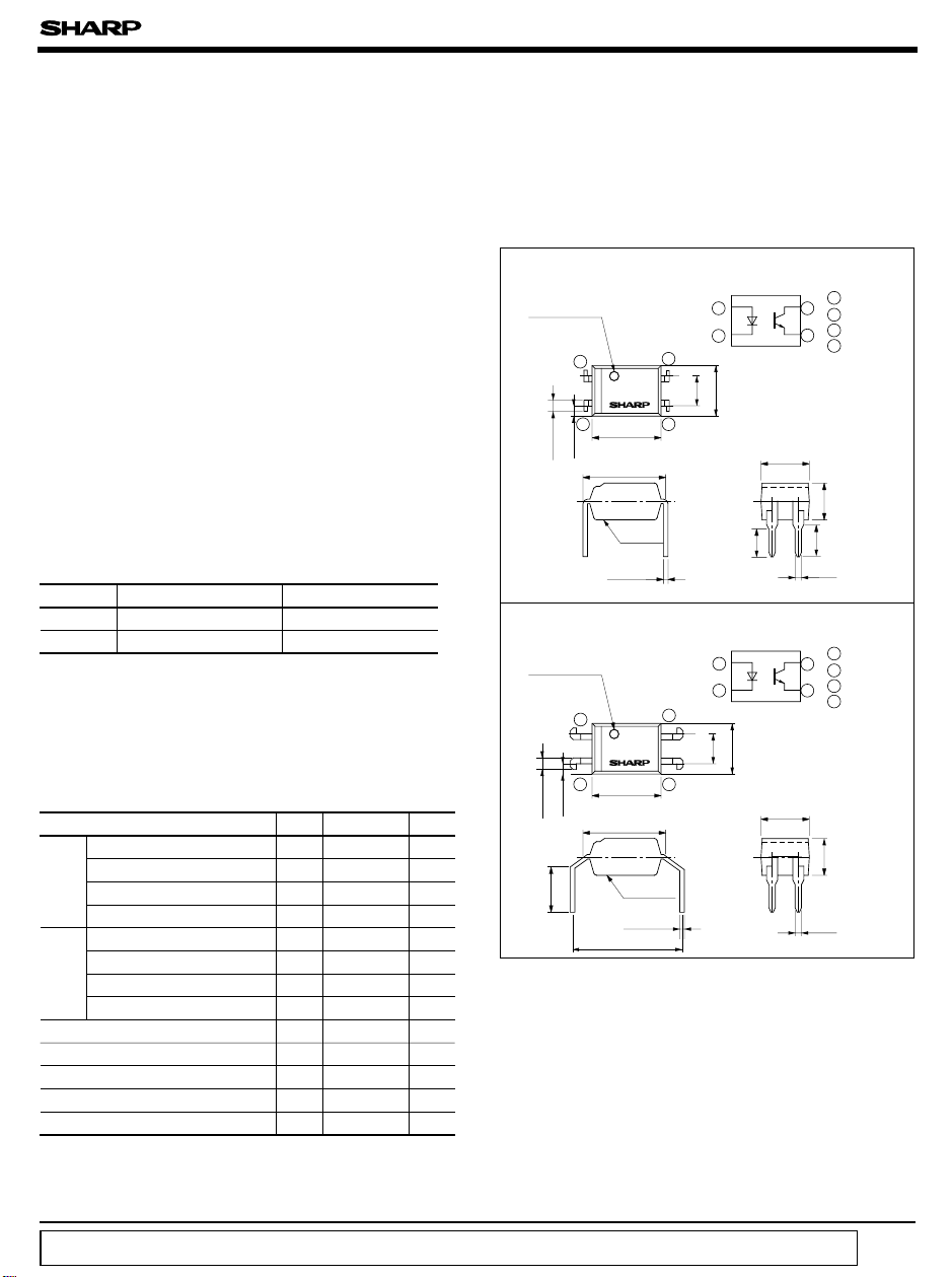
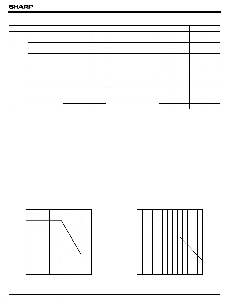
■ Outline Dimensions
PC123
)
Anode mark
1
2
± 0.1
± 0.3
1.0
1.2
PC123
± 0.3
6.5
± 0.3
7.62
Epoxy resin
0.26
4
3
± 0.1
Internal connection diagram
1
2
± 0.25
± 0.3
2.54
4.58
± 0.5
3.05
PC123F
1 Anode
4.58
± 0.3
4
3
± 0.1
0.5
2 Cathode
3 Emitter
4 Collector
± 0.5
3.5
kV
± 0.1
1
2
4
± 0.3
± 0.25
2.54
3
4.58
Anode mark
1
PC123
2
± 0.3
6.5
± 0.1
)
rms
± 0.3
1.0
1.2
MIN.
2.7
10.16
7.62
Epoxy resin
0.26
± 0.5
± 0.3
)
diagramInternal connection
˚C
˚C
“ In the absence of confirmation by device specification sheets, SHARP takes no responsibility for any defects that occur in equipment using any of SHARP's devices, shown in catalogs,
data books, etc. Contact SHARP in order to obtain the latest version of the device specification sheets before using any SHARP's device. ”
Page 2
PC123/PC123F
■ Electro-optical Characteristics
Parameter Symbol Conditions Unit
Forward voltage V
Input
Output
Transfer
characterisitics
Reverse current
Terminal capacitance C
Collector dark current I
Collector-emitter breakdown voltage
Emitter-collector breakdown voltage
Collector current I
Collector-emitter saturation voltage
Isolation resistance 5 x 10
Floating capacitance C
Cut-off frequency
Response time
Rise time t
Fall time t - 3 18
V
I
CEO
BV
BV
CE(sat
R
f
MIN. TYP. MAX.
IF= 20mA - 1.2 1.4 V
F
VR=4V - - 10 µA
R
V= 0, f= 1kHz - 30 250 pF
t
V
= 50V, I
CE F
CEOIC
ECOIE
C
ISO
f
c
r
f
= 0.1mA, IF= 0 70 - - V
=10µA, IF=0 6 - - V
IF= 5mA, VCE= 5V 2.5 - 20 mA
)
IF= 20mA, IC= 1mA - 0.1 0.2 V
DC500V, 40 to 60%RH
V= 0, f= 1MHz - 0.6 1.0 pF
VCE= 5V, IC= 2mA
RL= 100Ω, - 3dB
VCE= 2V, IC= 2mA
= 100Ω
R
L
= 0 - - 100 nA
10
11
10
- 80 - kHz
-418
(
Ta= 25˚C
- Ω
)
µ s
µ s
Fig. 1 Forward Current vs.
Ambient Temperature
60
50
)
mA
(
40
F
30
20
Forward current I
0
-30100 25 50 75 100 125
Ambient temperature Ta (˚C
Fig. 2 Diode Power Dissipation vs.
Ambient Temperature
)
100
mW
(
80
70
60
40
Diode power dissipation P
25
20
0
-30
)
0 50 100
Ambient temperature T
(˚C)
a
Page 3

PC123/PC123F
Fig. 3 Collector Power Dissipation vs.
Ambient Temperature
200
)
mW
(
150
C
100
50
Collector power dissipation P
0
-30
0 125
25 50 75 100
Ambient temperature T
(˚C)
a
Fig. 5 Peak Forward Current vs. Duty Ratio
10000
5000
)
2000
mA
(
1000
FM
500
200
100
50
Peak forward current I
20
10
5
-3
2
5
10
5
10
Duty ratio
-2
2
Pulse width <=100µs
Ta= 25˚C
-1
2
5
10
5
1
Fig. 7 Current Transfer Ratio vs.
Forward Current
300
)
250
%
(
200
150
100
Current transfer ratio CTR
50
0
0.1 1 10 100
Forward current I
F
(mA)
V
T
=5V
CE
= 25˚C
a
Fig. 4 Power Dissipation vs.
Ambient Temperature
250
)
mW
(
200
tot
150
100
Power dissipation P
50
0
0 25 50 75 100 125
-30
Ambient temperature T
(˚C)
a
Fig. 6 Forward Current vs.
Forward Voltage
1000
)
(
mA
F
500
200
100
= 75˚C
T
a
50
50˚C
0˚C
+ 25˚C
- 25˚C
20
10
Forward current I
5
2
1
0 0.5 1.0 1.5 2.0 2.5 3.0
Forward voltage V
(V)
F
Fig. 8 Collector Current vs. Collector-emitter
Voltage
= 25˚C
T
= 5mA
a
(V)
CE
60
54
)
(
mA
C
48
42
(
)
P
MAX.
C
36
30
24
Collector current I
18
12
6
0
= 30mA
F
I
= 20mA
F
I
= 10mA
I
F
I
F
012345678910
Collector-emitter voltage V
Page 4

PC123/PC123F
Fig. 9 Relative Current Transfer Ratio vs.
Ambient Temperature
150
IF= 5mA
=5V
V
)
%
(
CE
100
50
Relative current transfer ratio
0
-30
0 255075100
Ambient temperature T
(˚C)
a
Fig.11 Collector Dark Current vs.
Ambient Temperature
-5
10
5
)
-6
10
A
(
5
CEO
-7
10
5
-8
10
5
-9
10
5
Collector dark current I
-10
10
5
-11
10
- 30 0 20 40 60 80 100
Ambient temperature T
VCE= 50V
(˚C)
a
Fig.10 Collector-emitter Saturation Voltage vs.
Ambient temperature
0.16
)
V
(
)
0.14
sat
(
CE
0.12
0.10
0.08
0.06
0.04
0.02
Collector-emitter saturation voltage V
0.00
- 30 0 20 40 60 80 100
Ambient temperature T
= 20mA
I
F
I
= 1mA
c
(˚C)
a
Fig.12 Response Time vs.
Load Resistance
1000
100
)
µs
(
10
t
d
Response time
1
0.1
0.01 0.1 1 10 100
t
t
r
t
f
s
Load resistance (kΩ
V
=2V
CE
= 2mA
I
C
= 25˚C
T
a
)
Fig.13 Frequency Response
5
0
)
dB
(
-5
-10
Voltage gain Av
-15
-20
0.1 10 100
Please refer to the chapter “Precautions for Use ”
●
1
= 10k Ω
R
L
Frequency (kHz
1kΩ
)
V
I
C
T
CE
= 2mA
= 25˚C
a
=5V
100 Ω
1000
Fig.14 Collector-emitter Saturation Voltage vs.
Forward Currnt
)
V
(
5.0
)
sat
(
4.5
CE
4.0
3.5
I
= 0.5mA
C
1mA
3mA
5mA
7mA
3.0
2.5
2.0
1.5
1.0
0.5
Collector-emitter saturation voltage V
0
02468101214161820
Forward current I
F
(mA)
T
= 25˚C
a
 Loading...