

Page 1
PC 1202-A
PC 1202-A
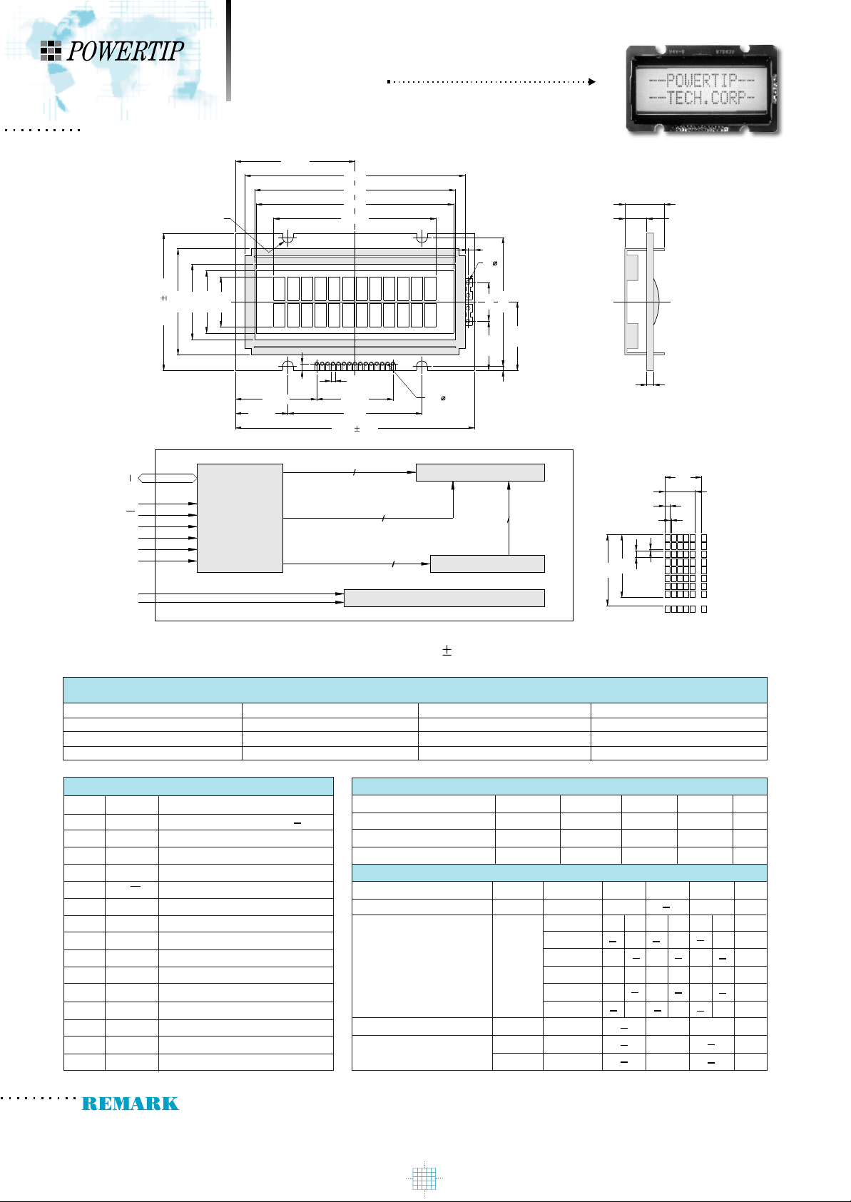
OUTLINE DIMENSION & BLOCK DIAGRAM
27.85
24.7
17.5
11.7
14.5
32.0 0.5
1
(P1.27 x 14)
1.5
18.96
12.25
55.7 0.5
51.3
46.7
46.0
37.854-R1.25
1.0
17.78
31.2
H1
H2
1.5
4- 1.0
K
9.0
30.0
A
16.0
15
15- 0.7
11.5
1.0
1.6
DB7
DB0
R/W
RS
Vss
Vdd
Vo
E
A
K
LCD
CONTROLLER
LSI
The tolerance unless classified 0.3mm
Overall Size
View Area
Dot Size
Dot Pitch
PIN ASSIGNMENT
Pin no. Symbol Function
Power supply(GND) / LED B/L( )
Power supply(+)
Contrast Adjust
Vo
Register select signal
Data read / write
Enable signal
E
Data bus line
Data bus line
Data bus line
Data bus line
Data bus line
Data bus line
Data bus line
Data bus line
Power supply for LED B/L (+)
10
11
12
13
14
15
Vss/K
1
2
Vdd
3
4
RS
5
R/W
6
7
DB0
8
DB1
9
DB2
DB3
DB4
DB5
DB6
DB7
A
COM 16
SEG 40
CONTROL SIGNALS 4
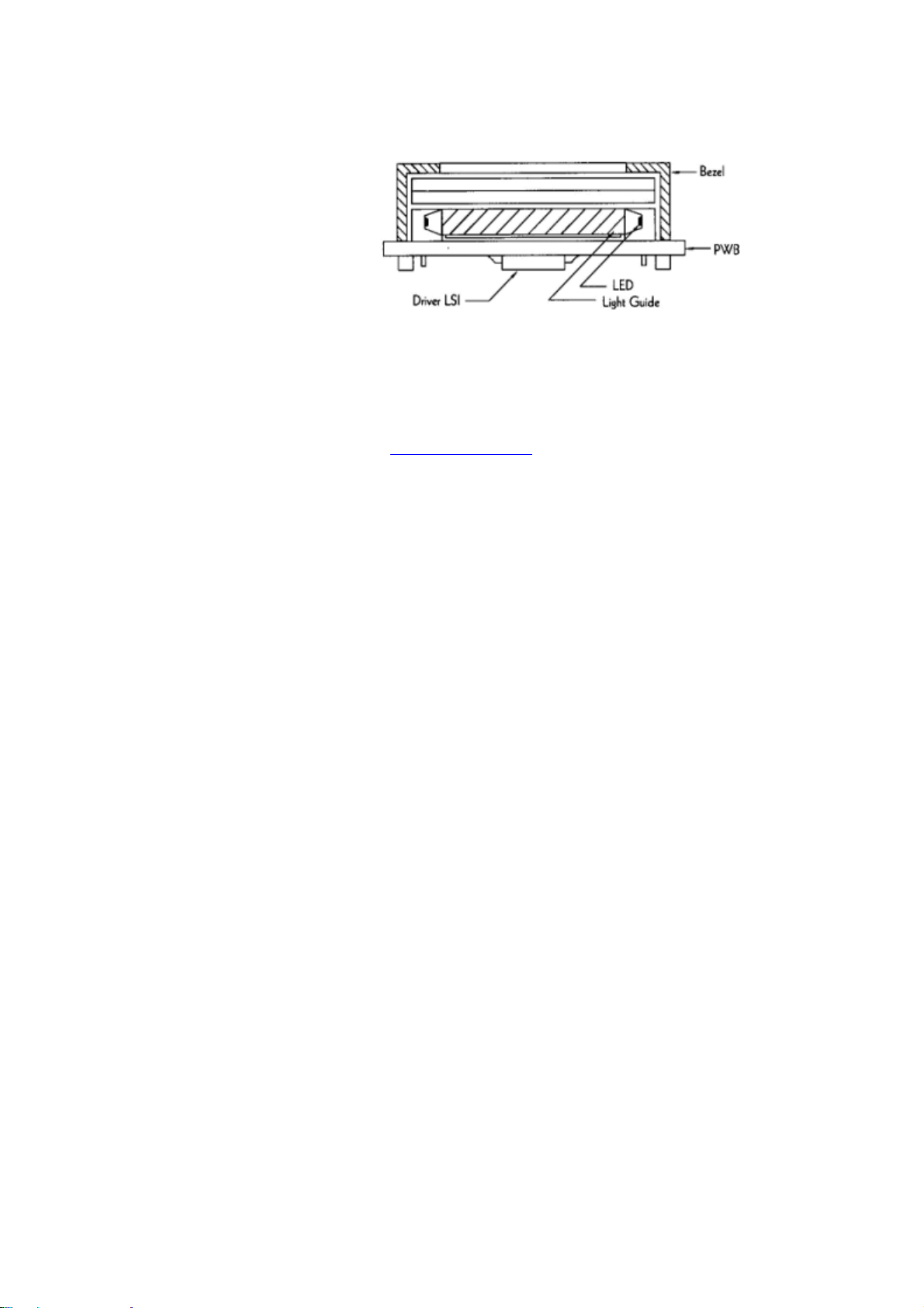
BACKLIGHT
LCD PANEL
SEGMENT DRIVER
MECHANICAL SPECIFICATION
55.7 x 32.0
46.7 x 17.5
W /O B/L
0.45 x 0.60
0.55 x 0.70
ABSOLUTE MAXIMUM RATING
Item
Supply for logic voltage
LCD driving supply voltage
Input voltage
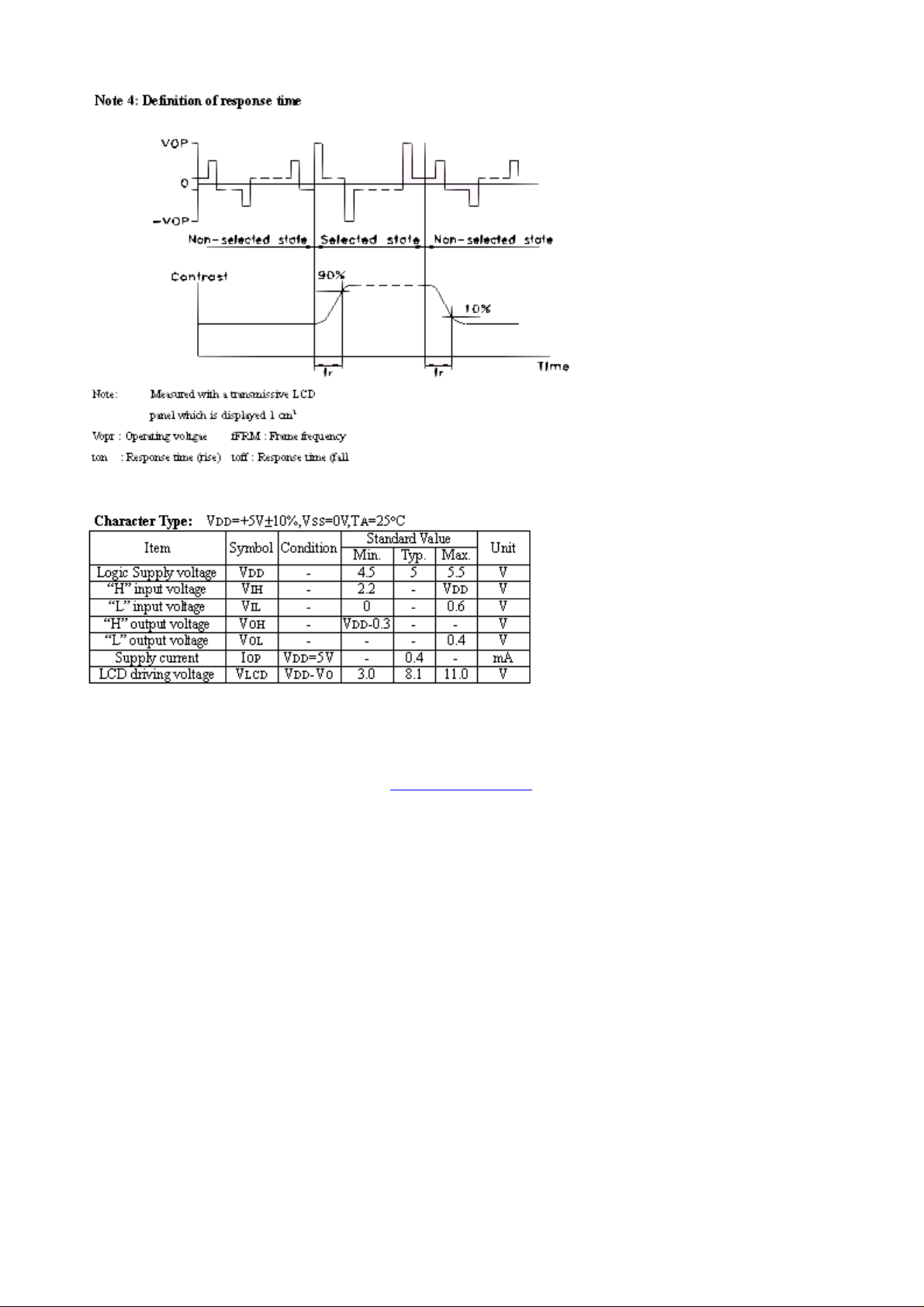
ELECTRICAL CHARACTERISTICS
Item
Power supply voltage
LCD operation voltage
LCM current consumption (No B/L)
Backlight current consumption
SEG 20
Module
EL B/L
LED B/L
Symbol
Vdd-Vss
Vdd-Vee
Vin
Symbol
Vdd-Vs
Vop
Idd
LED/edge VB/L=4.2V
LED/array
6.2
Condition Min.
25oC
25oC
25oC
Condition
25oC
Top
-20oC
0oC
25oC
50oC
70oC
N W
4.5
4.1
3.8
Vdd=5V
VB/L=4.2V
0.6
3.2
0.1
0.1
2.65
0.45
5.5
H2 / H1
5.1 / 9.2
5.1 / 9.2
8.7 / 12.8
Max.
7.5
6.4
1.5
40
80
7
13
Vdd+0.3
Max.
N W
5.1
4.7
4.4
6
2.5
7.9
6.7
6.3
-0.3
-0.3
-0.3
Typical
Min.
2.7 5.5
N W
7.1
4.6
6.1
4.4
4.1
5.7
Units
V
V
V
Units
V
V
V
V
V
V
V
mA
mA
mA
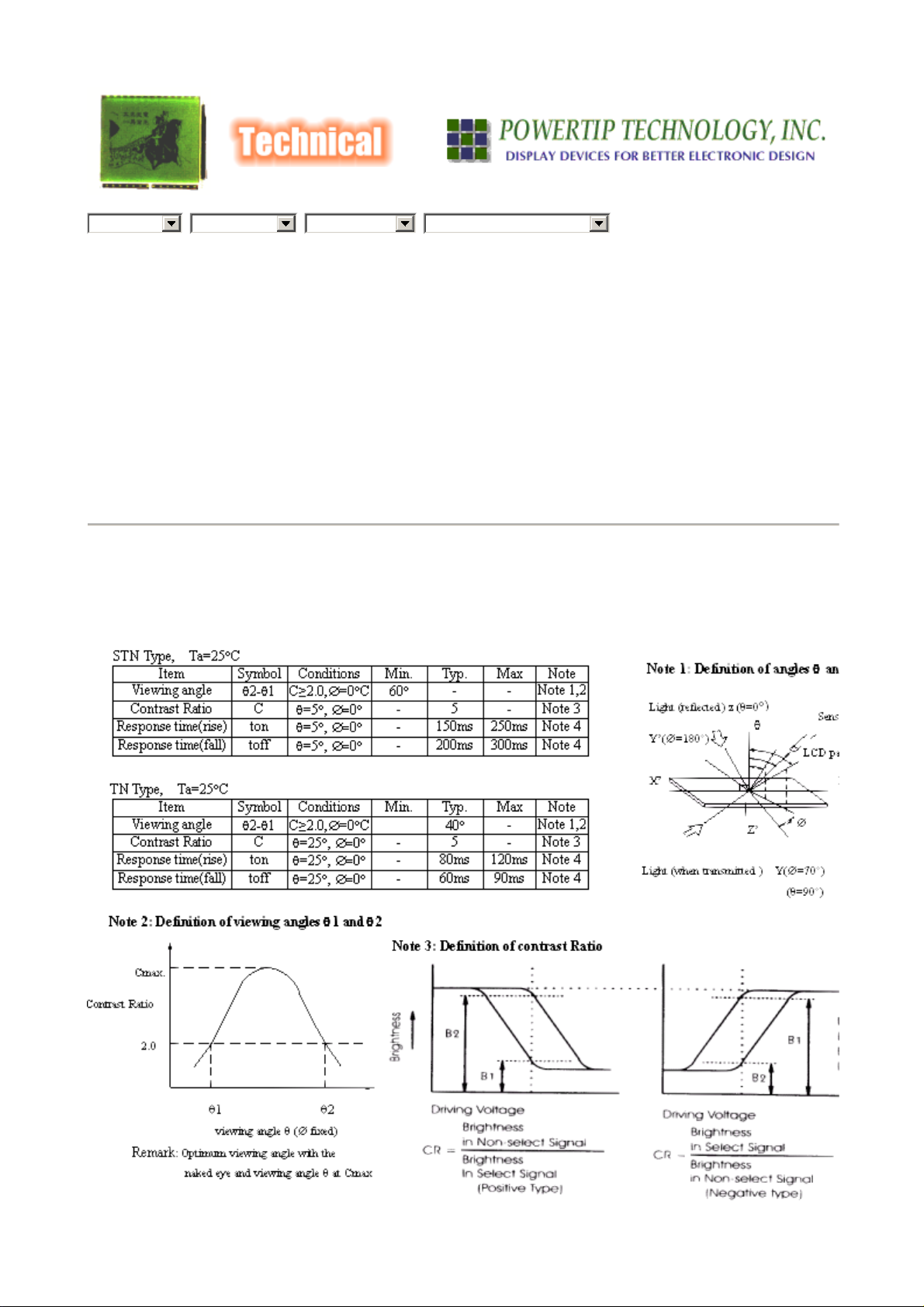
LCD option: STN, TN, FSTN
Backlight Option: LED Backlight feature, other Specs not available on catalog is under request.
Page 2
CODING SYSTEM FOR LCD MODULE
P C 1 6 0 2
1 2 3 4 5 6 7 8 9 10 11
NO Cod e valu e Descr iption Type
1
P Powertip products Brand
C Character
G Graphic
2
S Engineer sample
T Total solution
-
-
-
Module type
08.16.20.24
3
120.122.128
01.02.03.04
4
32.64.128
A Without backlight
B EL backlight, Blue-green
D EL backlight, Yellow-green
E EL backlight, White
F CCFL backlight, White
L LED backlight, Yellow-green
5
M LED backlight, Amber
N LED backlight, Red
O LED backlight, Orange
P LED backlight, Pure-green
...
...
...
...
Column dots (for graphic modules)
Characters per line (for character modules)
Row dots (for graphic modules)
Lines (for character modules)
Characters per
line or row dots
Lines or column
dots
Backlight mode
(Type Color)
+
S LED backlight, Green
U LED backlight, Blue
W LED backlight, White
R
6
Y Straight pin-header
Z Right angle pin-header
None (*1) TN positive, Gray
7
N TN negative, Blue
S STN positive, Gray
Standard (through hole, cable, connector and
etc.)
Connecting type
LCD mode
(Type Color)
+
Page 3
U
STN positive, Y ellow-green
M
STN negative, Blue
7
F
T
0~ Z Series number Model name
8
FSTN positive, White
FSTN negative, Black
manufacturer / character pattern
IC
LCD mode
(Type+Color)
00~ZZ
9
NN
A
D
G
J
B
E
10
H
K
/total solution series number
Without
Reflective /Normal temp. /6:00 direction
controller
Reflective /Normal temp. /12:00 direction
Reflective /Extended temp. /6:00 direction
Reflective /Extended temp. /12:00 direction
Transflective /Noraml temp. /6:00 direction
Transflective /Noraml temp. /12:00 direction
Transflective /Extended temp. /6:00 direction
Transflective /Extended temp. /12:00 direction
Polarizer type/
LCD T emperature
range/
Vi ewin g direction
* 2
C
F
I
L
No code value
Transmissive /Normal temp. /6:00 direction
Transmissive /Normal temp. /12:00 direction
Transmissive /Extended temp. /6:00 direction
Transmissive /Extended temp. /12:00 direction
Standard product
11
01~ZZ Special
(*1) Without code value
(*2)
(*3) Check with our sales for available combinations.
Character Pattern
English / Japanese EA HO/HA/HC SO NO WA AO JA YA
English / Europe EB
English / France EC S3 N3
English / Russia EH SH NH
English / Chinese HH
English / Hebrew S4/S8 N4/N8
Note:
A: APANPEC LSI M: MOTOROLA LSI R: SHARP LSI W: SITRONIX LSI
E: ESPON LSI N: NOVATECH LSI S: SUMSUNG LSI Y : SANYO LSI
H: HITACHI LSI O: OKI LSI T: TOSHIBA LSI
J : JRC LSI P: PHILIPS LSI U: UMC GROUP LSI
code
H2/HB/HC/H
Character
S5/S6 N5/N6/NI WB/W 5 JB
U
Version
Graphic
E4
TA
Page 4
CODING SYSTEM FOR OTHER PRODUCTS
P D
NO CODE VALUE DESCRIPTION TYPE
PD Products
1
2
IN05300,IN05500...
NOTE:The code
value
-
1 2
Powertip design
Product
and
characteristic
length
product
product
of
characteristic
are
unlimited
Types
Page 5
Page 1 of 2Powertip Technology, Inc.
PROFILE
NEWS TECHNICAL PRODUCTS
Typtical/Electrical Characteristics of LCD Modules
z Optical Characteristics Of LCD Modules
z
Electrical Characteristics Of LCD Modules
Optical Characteristics Of LCD Modules
STOCKING
DISTRIBUTOR
SALES
NETWORK
CONTACT
US
11/10/2004http://www.powertipusa.com/char.htm
Page 6
Page 2 of 2Powertip Technology, Inc.
Electrical Characteristics Of LCD Modules
© 2001, All rights reserved.
Powertip Technology, Inc.
18 Technology Drive, STE 161, Irvine, CA 92618
Phone: (949) 585-9888, Fax: (949) 585-9889
sales@powertipusa.com
11/10/2004http://www.powertipusa.com/char.htm
Page 7
Page 1 of 3Powertip Technology, Inc.
PROFILE
STOCKING
NEWS TECHNICAL PRODUCTS
DISTRIBUTOR
Backlight options for LCD modules
z
EL Backlight
z CCFL Backlight
z LED Backlight
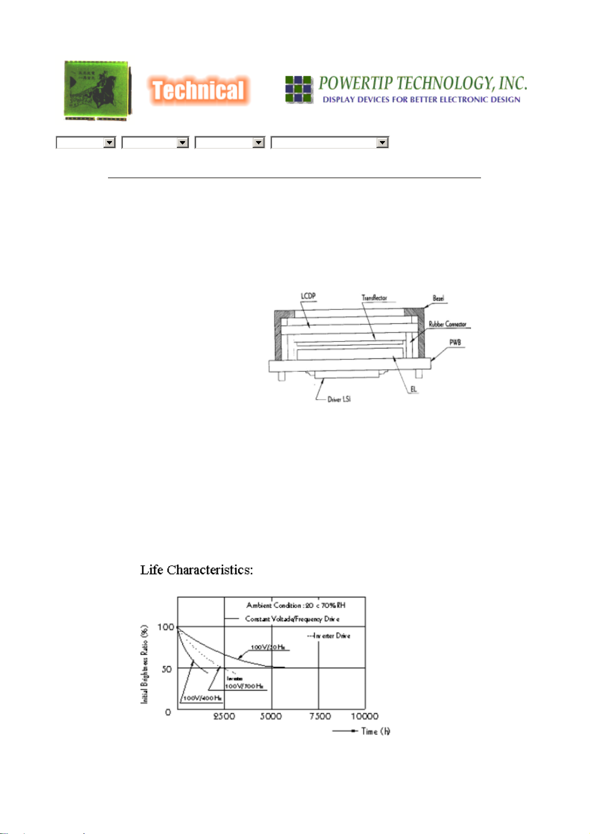
EL Backlight Precautions For Handling LCD Modules
Flat surface light source offers simple and even illumination over large area.
z Max.1.3mm thickness ( Max.
1.5mm for lead portion )
z
Wide driving condition, 601,000Hz at 150V AC Max. With
inverter, step-up voltage from
1.5V battery is available.
z
Emitted colors are blue-green,
yellow-green and white.
z Operating characteristics of
PC2002-A SERIES is 110V,
400Hz, 8mA, ( Ta=20°C, 60%
RHæ)
z
Temperature Range:
{ Operating 0°C~ +50°C
{
Storage -20°C~ +60°C
SALES
NETWORK
CONTACT
US
Inverter for EL Backlight Drive:
z Requires an inverter to operate the EL panel with a battery or DC power supply.
z
Low inverter loss and high light efficiency since it is designed for EL backlight.
z Constant power consumption during operation, given temperature change for extended
hours. This is characterized by the constant sup ply current, which minimizes the
brightness change of the EL panel.
CCFL Backlight( Cold Cathode Fluorescent Lamp )
12/10/2004http://www.powertipusa.com/bl.htm
Page 8
Bright
white
color
of
light
source
offers
clear
and
even
illumination
over
large
viewing
area.
Features:
{
High
Brightness
{ Long life time.
{
Low Power consumption
{ White color emitted
Page 2 of 3Powertip Technology, Inc.
Direct Illumination
{ Suitable for multi-color and / or dot matrix LCDP.
Edge
Illumination
{ Thin
structure
type
of
even
illumination
emits
light
from
tube
like
light source over a large area.
Precaution
{ Inverter for CCFL use output high pressure AC current. Therefore, please pay
attention when you handleinverter and power supply cable of LCD backlight.
LED Backlight
Long life, low power consumption and requires a simple power supply. Available colors
are red, green and orange, available in array type illumination or edge illumination.
Features:
{ Low driving voltage ( DC ) and does not require an inverter.
{
Long life of 100,000 hours ( average )
{ No noise occurrence.
Various colors available in red, green and orange etc. (multi-color by alternative switch is
also available)
{ Operating characteristics of PC2002-A series is 4.2V, 210mA, 250cd/m
Array
Illumination
{ A
grid
array
of
leaÍs
provide
even
illumination.
12/10/2004http://www.powertipusa.com/bl.htm
Page 9
Edge Illumination
{ Combination LED with a light guide offers a thin structure type of illumination.
© 2001, All rights reserved.
18 Technology Drive, STE 161, Irvine, CA 92618
Phone: (949) 585-9888, Fax: (949) 585-9889
Powertip Technology, Inc.
sales@powertipusa.com
Page 3 of 3Powertip Technology, Inc.
12/10/2004http://www.powertipusa.com/bl.htm
Page 10
Page 1 of 3Powertip Technology, Inc.
PROFILE
STOCKING
NEWS TECHNICAL PRODUCTS
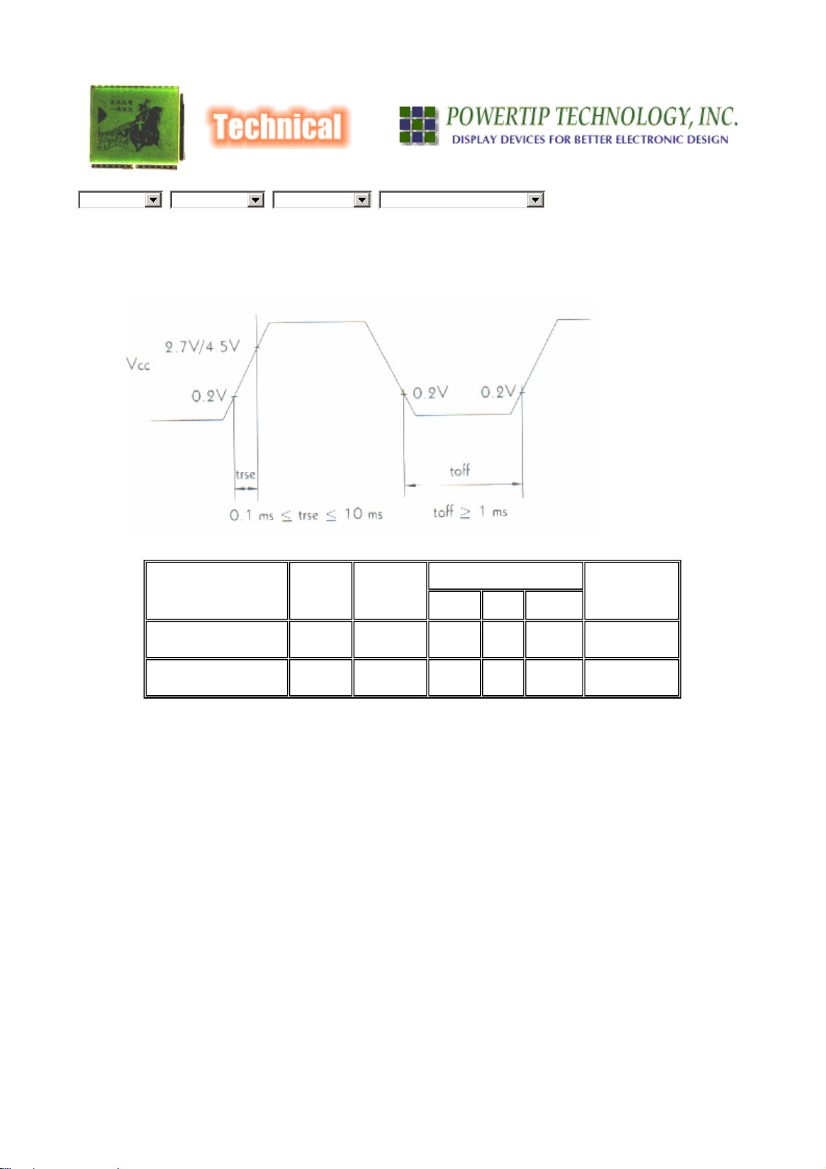
Power Supply Reset
The internal reset circuit will be operating properly when the following power supply conditions are
satisfied. If it is not operating properly, please perform the initial setting along with the instruction.
Item
Measuring
Symbol
Condition
Standard Value
Min. Typ. Max.
DISTRIBUTOR
SALES
NETWORK
Unit
CONTACT
US
Power Supply RISE
Time
Power Supply OFF
Time
Reset function
Initialization made by internal reset circuit
{
The HD44780 automatically initializes (resets) when power is supplied (builtin internal reset
circuit).
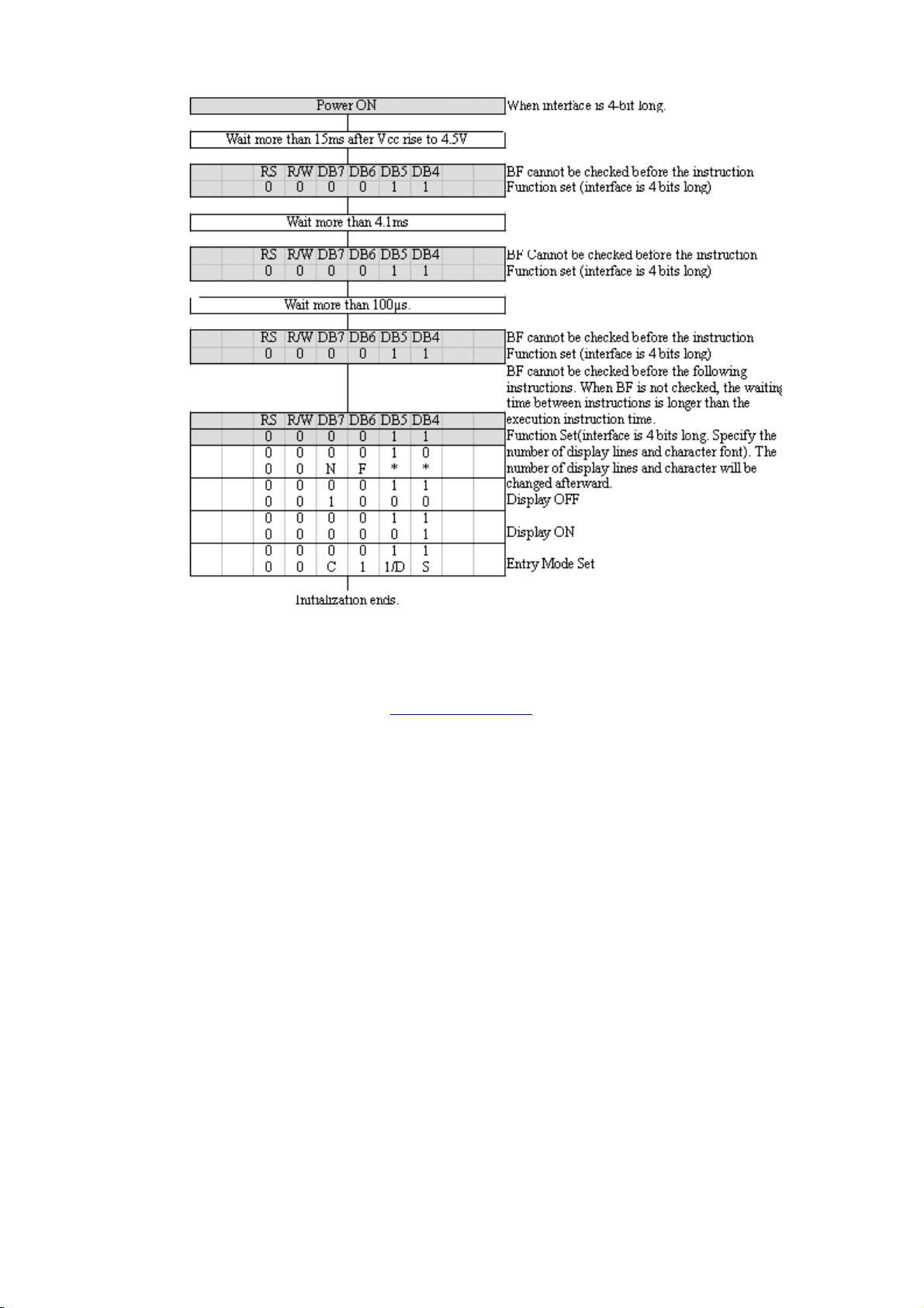
{ The following instructions are executed during initialization.
The busy flag (BF) is kept in busy state until initialization ends. (BF=1) The busy
state is 10ms after Vdd reaches 4.5V.
1. Display clear
2. Function set
DL=1:8 bit long interface data
DL=0:4 bit F=0:5 * 7 dots character font
N=1:2 lines
N=0:1 line
3. Display ON/OFF control
D=0:Display OFF C=0:Cursor OFF
B=0:Blink OFF
4. Entry mode set
1/D= 1:+1(increment) S=0:No shift
trse
toff
-----
-----
0.1 -----
1
-----
10
-----
mS
mS
Note: When the power supply conditions, using internal reset circuit is not satisfied,
the internal reset circuit will not function properly and initialization will not be
performed.Please initialize using the MPU along with the instruction set.
11/10/2004http://www.powertipusa.com/ps.htm
Page 11
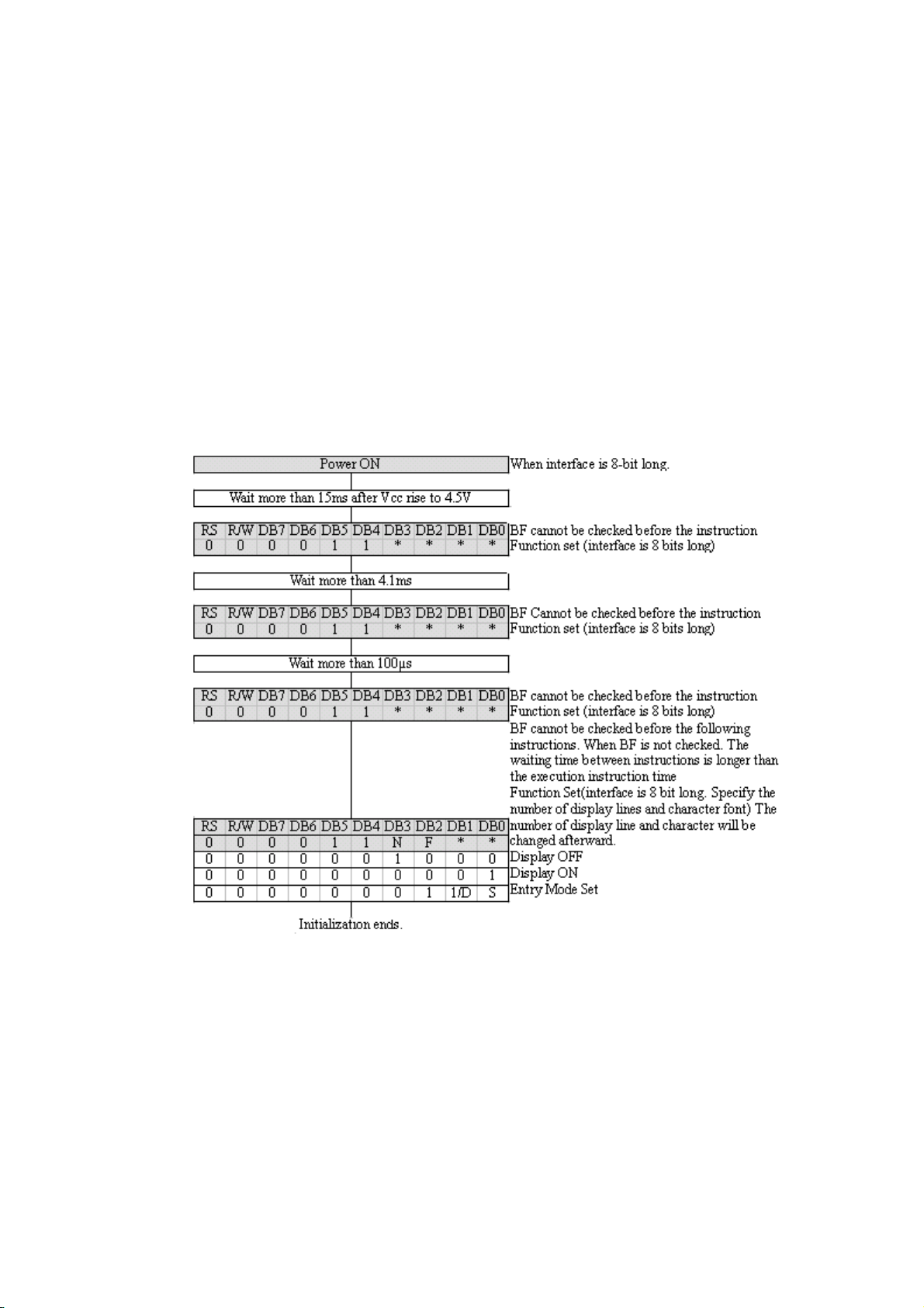
Initialization along with instruction
If power supply conditions are not satisfied, for the proper operation of the internal reset circuit, it
is necessary to initialize using the instructions.
Please use the following procedures.
Page 2 of 3Powertip Technology, Inc.
11/10/2004http://www.powertipusa.com/ps.htm
Page 12
Page 3 of 3Powertip Technology, Inc.
© 2001, All rights reserved.
18 Technology Drive, STE 161, Irvine, CA 92618
Phone: (949) 585-9888, Fax: (949) 585-9889
Powertip Technology, Inc.
sales@powertipusa.com
11/10/2004http://www.powertipusa.com/ps.htm
Page 13
Page 1 of 3Powertip Technology, Inc.
PROFILE
NEWS TECHNICAL PRODUCTS
Interface With MPU
z
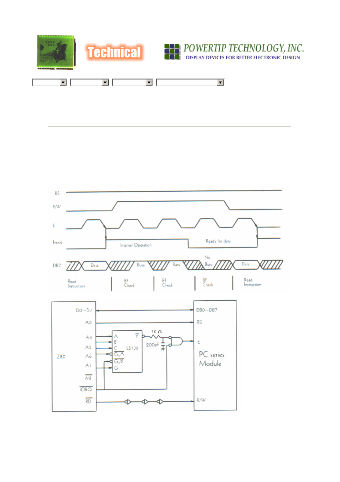
Example of interfacing to an 8-bit MPU(Z80)
z Example of interfacing to a 4-bit MPU
z If interface data is 4-bits long
z If interface data is 8-bits long
Example of interfacing to an 8-bit MPU(Z80)
STOCKING
DISTRIBUTOR
SALES
NETWORK
CONTACT
US
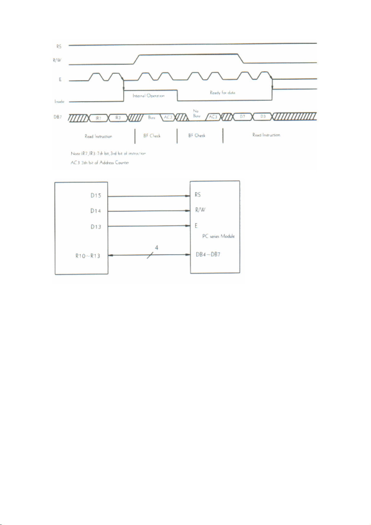
Example of interface to a 4-bit MPU
Interface to a 4-bit MPU can be made through the I/O port of the 4-bit MPU. If there are sufficient I/O ports,
data can be transferred at 8-bit cycles, however, if there are not, data transfer can be accomplished by two
cycles of 4-bit transfers (select interface as 4-bits long). Please take into account that 2 cycles of the BF check
will be necessary and the timing sequence will prove to be complicated.
11/10/2004http://www.powertipusa.com/mpu.htm
Page 14
Page 2 of 3Powertip Technology, Inc.
Features:
1. Interface to an 8-bit or 4-bit MPU is available.
2. 192 types of alphanumerics, symbols and special characters can be displayed with the multi
built-in character generator(ROM).
3. Other preferred characters can be displayed by character generator(RAM)
4. Various instructions may be programmed.
Clear display
Cursor at home
On/Off cursor
Blink character
Shift display
Shift cursor
Read/write display data, etc.
5. Compact and light weight design which can easily be integrated into end products.
6. single power supply +5V drive(except for extended temp. type).
7. Low power consumption.
Interface between data bus line and 4-bit or 8-bit MPU is available.
Data transfer requires two cycles in case of a 4-bit MPU, and once in case of an 8-bit
MPU.
If Interface Data Is 4-bit long
z
Data transfer is accomplished through 4 bus lines from DB4 to DB7.(while the rest of 4 bus lines from
DB0 to DB3 are not used.)
z Data transfer is completed when 4-bits of data is transferred twice.(upper 4-bits of data, then lower 4-
bits of data.)
11/10/2004http://www.powertipusa.com/mpu.htm
Page 15

If Interface Data Is 8-bits Long
z Data transfer is made through all 8 bus lines from DB0 to DB7.
© 2001, All rights reserved.
Powertip Technology, Inc.
18 Technology Drive, STE 161, Irvine, CA 92618
Phone: (949) 585-9888, Fax: (949) 585-9889
sales@powertipusa.com
Page 3 of 3Powertip Technology, Inc.
11/10/2004http://www.powertipusa.com/mpu.htm
Page 16

Page 1 of 2Powertip Technology, Inc.
PROFILE
NEWS TECHNICAL PRODUCTS
STOCKING
DISTRIBUTOR
SALES
NETWORK
CONTACT
US
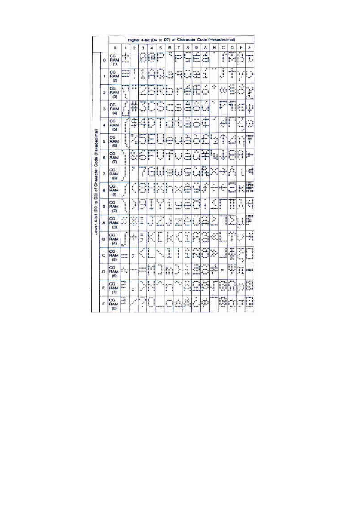
Standard Character Pattern
z
Character Pattern (WB)
z Character Pattern (HC)
z
Character Pattern (NI)
z Character Pattern (JA)
z
Character Pattern (SO,WA)
z Character Pattern
z Character Pattern (N5)
z Character Pattern
z Character Pattern (N4)
z
Character Pattern (TA)
z Character Pattern (NH)
z
Character Pattern (YA)
11/10/2004http://www.powertipusa.com/pat.htm
Page 17
Page 2 of 2Powertip Technology, Inc.
© 2001, All rights reserved.
18 Technology Drive, STE 161, Irvine, CA 92618
Phone: (949) 585-9888, Fax: (949) 585-9889
Powertip Technology, Inc.
sales@powertipusa.com
11/10/2004http://www.powertipusa.com/pat.htm
Page 18
Page 1 of 6Powertip USA
PROFILE
Q & A
NEWS TECHNICAL PRODUCTS
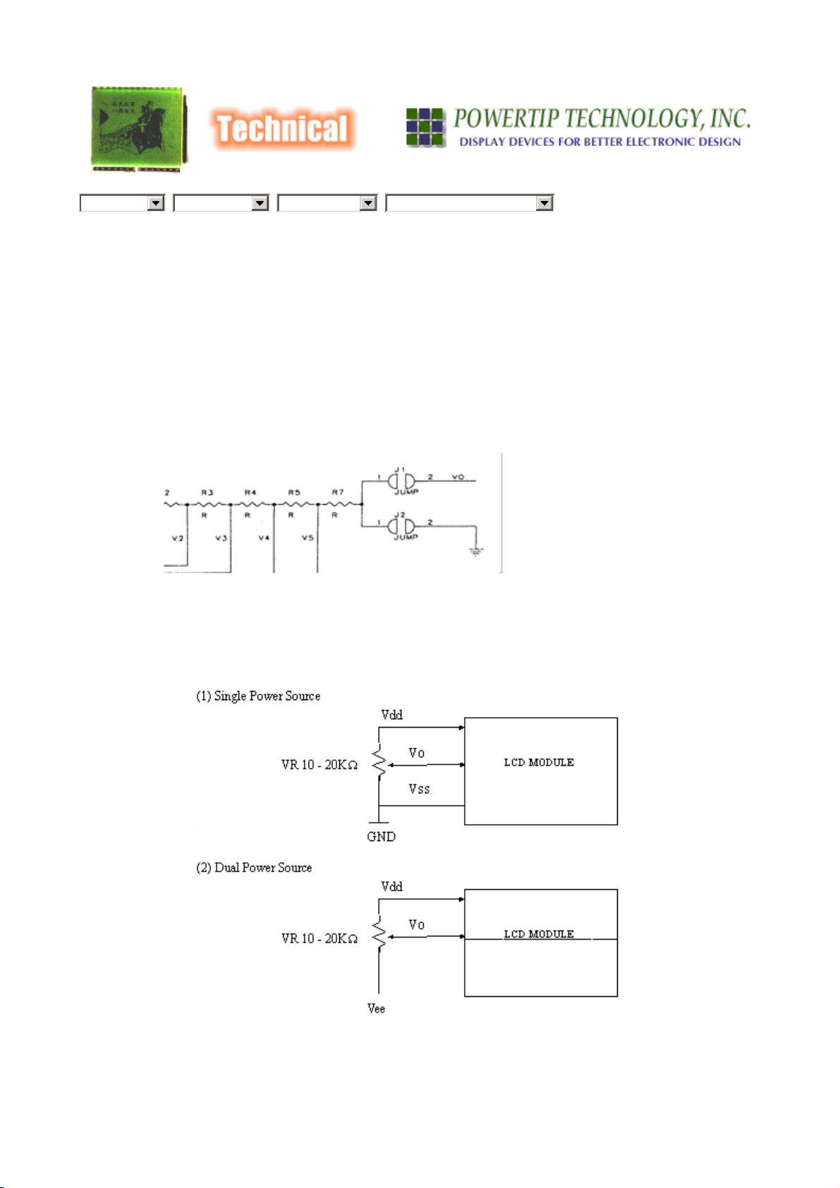
1. Adjusting the contrast of a character LCD module.
There are two means of adjusting the contrast: Please refer to the following drawing:
STOCKING
DISTRIBUTOR
SALES
NETWORK
CONTACT
US
1. Internal: J2 short, add the appropriate resister to R7 for contrast control.
2. External: J1 short, R7=0, By adding a VR the contrast can be controlled externally.
Please note the following diagram:
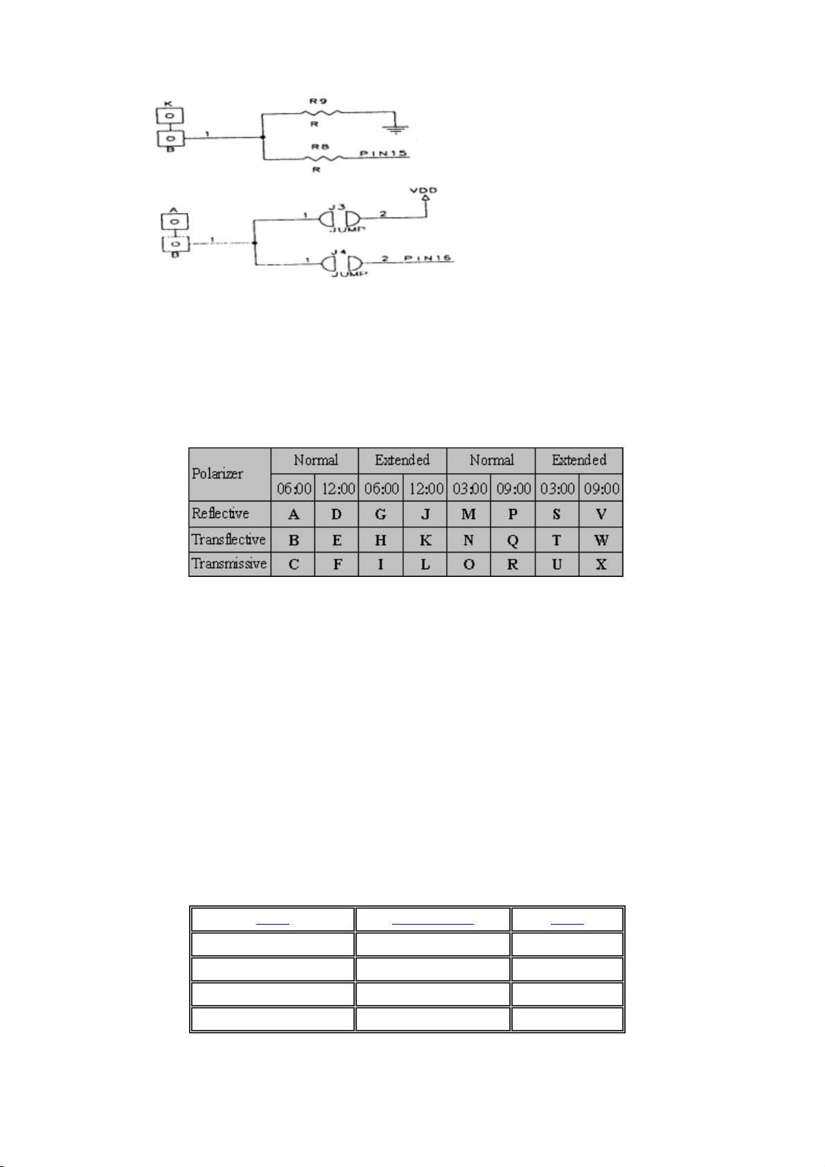
2. Connecting and powering the backlight.
There are two means of connecting and powering the backlight. Please refer to the below
diagrams:
11/10/2004http://www.powertipusa.com/qa.htm
Page 19
Page 2 of 6Powertip USA
1. PINS 1 & 2 (Vdd & Vss): J3 short, by adding a resistor on R9.
2. PINS 15 & 16: J4 short, by adding a resistor on R8.
NOTE: The brightness can be controlled by the value of R8 or R9.
3. Reference table for establishing the relationship between the temperature
range, viewing direction and type of polarizer:
4. Differences between a driver IC, a controller IC and a controller/driver IC:
Driver IC
a "segment" driver. Common drivers output signals to create the rows or number of
lines while the segment drivers output the necessary signals to create the characters
or columns.
Controller IC
stores this data in RAM. This data is then converted into a serial character pattern and
transferred to the LCD driver IC.
Driver/Controller IC
data from the MPU and stores it in RAM. It accepts commands directly from the MPU
for both the common and segment drivers.
: There are two types of driver IC's. One is a "common" driver and the other
: This IC receives data written in ASCII or JIS code from the MPU and
: It is most commonly found in a graphics module. It receives
5. Following is the minimum dot size and pitch on the LCD, the ITO line on
the LCD and the elastomer (zebra) connector:
ITEM
LCD Dots 0.22mm 0.02mm
LCD ITO lines S=0.075, C=0.08mm 0.03mm
Dots or Lines Gaps
Rubber Connectors 0.025mm 0.025mm
Heat Seal 0.09mm 0.09mm
6. Advantages and disadvantages of backlight versions:
11/10/2004http://www.powertipusa.com/qa.htm
Page 20
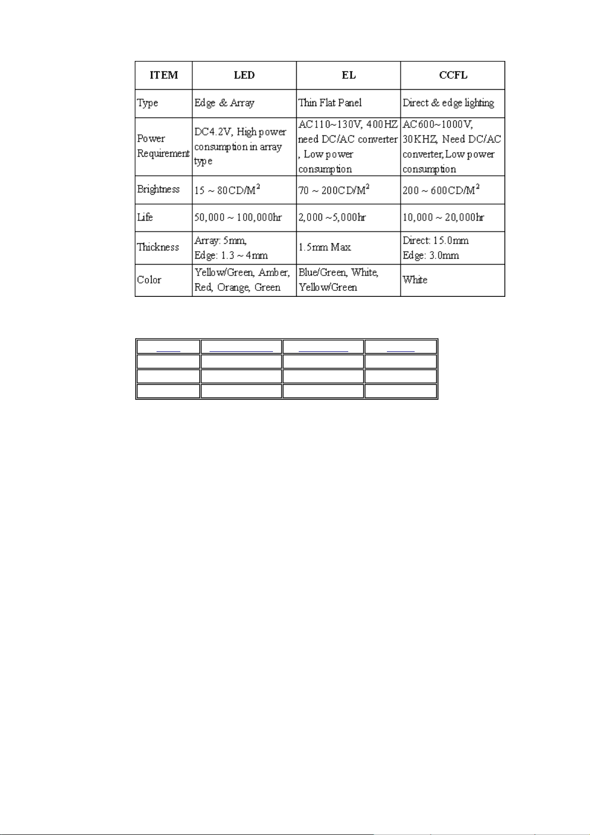
Page 3 of 6Powertip USA
7. Comparison between TN, STN and FSTN technologies:
ITEM Contrast Ratio View Angle COST
TN 3 3 3
STN 2 2 2
FSTN 1 1 1
Remarks: with 1 being the best or most expensive and 3 the worst or least expensive.
8. Differences between reflective, transflective and transmissive displays
Reflective
front of the display. Reflective displays require ambient light for the light source since
there is no backlight.
Transflective
to pass through the back, as well as reflecting light from the front.
Transmissive
laminated to the rear polarizer. A backlight must be used with this type of LCD
configuration. The most common is a transmissive negative image.
9. Considerations for attaining a 3.0 Volt LCD module:
: Such display includes a diffuser. This layer reflects the light that enters the
: As type of backing which is bonded to the rear polarizer. Enables light
: A type of LCD which does not have a reflector or transflector
IC: Choose the ICs that can be driven at 3.3V or less. Below is a list of IC's that can
accomplish this requirement:
Controller:
KS0066U 2.7 ~ 5.5V
KS0070B 2.7 ~ 5.5V
HD44780U 2.7 ~ 5.5V
Driver:
11/10/2004http://www.powertipusa.com/qa.htm
Page 21

KS0065 2.7 ~ 5.5V
KS0063 2.7 ~ 5.5V
SED1181 5.0V min.
LCD panel: The driving voltage for most all LCD panels is above 3.3V. It is necessary
to then add a "negative voltage" IC on the PCB of the module or to the customer's
motherboard to raise the voltage. A couple of NV generators is as follows:
NV IC: SCI7661 3X with temperature compensation.
SCI7660 2X, dice font available (at a much less expensive cost).
If a NV IC must be incorporated onto the module PCB, there is apt to be
two possible considerations:
1. Tooling cost
Page 4 of 6Powertip USA
2. The PCB is too small to accommodate the NV IC. If there is not
sufficient space, a possible solution would be to replace one controller
with a driver, with single controller (such as replacing a KS0066(U) &
KS0065(B) with a KS0070). The per unit cost will be a little greater but it
will save overall space on the PCB and eliminate having to re-tool the
PCB.
Some TAB IC's such as SED1560 series include a power circuit, which
can amplify the input voltage to drive the LCD. In this case it is not
necessary to add a NV IC to raise the voltage.
C. Backlight:
CCFL & EL: These backlight options require an inverter. The inverter
chosen cannot exceed 3.3 Volts.
LED: In an attempt to achieve this 3.3V requirement it is necessary to
use an edge-lit LED. Note this edge-lit LED will still consume a large
current.
10. Reference to Viewing angle:
Viewing Angle is the direction by which the display will look best. This is established
during the manufacturing process and can not be changed by rotating the polarizer.
Viewing direction is specified in terms of a clock position, such as 6:00 & 12:00.
Please refer to the following drawing:
11/10/2004http://www.powertipusa.com/qa.htm
Page 22

Page 5 of 6Powertip USA
11. Clarification to the term "rainbow" effect:
This refers to a red and green circle or rainbow on the LCD glass. The LCD panel
under uneven pressure causes this problem from the bezel. It is very common in LCD
modules and normally it will not affect the performance or the appearance of the
display when operational.
12. Pin assignments for a Character module:
Example of a standard 14-pin character module:
PIN 1: Vss
PIN 2: Vdd
PIN 3: Vo
PIN 4: RS
PIN 5: R/W
PIN 6: Enable
PIN 7 ~ 14: DB0 ~ DB7
13. What is temperature compensation and why is required
A LCD operating voltage varies at different temperatures. The operating voltage must
rise as temperature lowers or the contrast will degrade. Conversely, the operating
temperature must fall as the temperature rises or the contrast will degrade. For this
reason it is often a requirement, with graphics modules, to control the input voltage
accordingly. The temperature compensation circuit is the circuit that controls the input
voltage as the temperature changes. This temperature compensation circuit can be
located on the LCD module or on the customer's motherboard.
14. Troubleshooting a LED backlit module in which the display is turning
dark:
This problem is more than likely caused by the temperature rise from the LED
backlight. In this case the LED backlight has consumed too much of the power. When
the temperature rises, the V
high. The result is a poor contrast and the display becoming too dark. The solution
would be to lower the power consumption of the LED. This can be accomplished by
raising the value of R8 or R9 to reduce the current to the LED backlight.
15. How to control the LED backlight on a 14-pin module:
becomes lower causing the input voltage to be too
LCD
Short J2, the Vdd is controlling the input to the LED backlight. In addition, it is
necessary to place a current limiting resistor to lower the voltage from 5V to 4.2V.
Note: If the LED is drawing too much current, it may cause the Vdd † Vo too low and
the contrast becomes poor. If this should occur increasing the value of R9 should
decrease the current draw to the LED backlight or another approach would be to
increase the voltage input to the LCD by decreasing the value of R7.
16. Examples of the current consumption of an LED backlit, EL backlit and
the LCD for the following modules:
11/10/2004http://www.powertipusa.com/qa.htm
Page 23

Page 6 of 6Powertip USA
Products
PC1602-F 1.3mA 120mA 3.26mA
PC2002-B 1.8mA 200mA 5.3mA
PC2004-A 1.8mA 260mA 7.2mA
PC4004-A 2.2mA 440mA 7.5mA
LCM LED EL
17. Following is the Vop range for a Character and Graphics LCD module:
LCD Type Vop for N.T. Vop for W.T.
Character 4.2 ~ 4.8V 5 ~ 9V
Graphic 5.5 ~ 26V 6 ~ 28V
Note: N.T. = normal temperature
W.T.= wide temperature
© 2001, All rights reserved.
Powertip Technology, Inc.
18 Technology Drive, STE 161, Irvine, CA 92618
Phone: (949) 585-9888, Fax: (949) 585-9889
sales@powertipusa.com
11/10/2004http://www.powertipusa.com/qa.htm
Page 24

ST
Sitronix
Features
!"
5 x 8 and 5 x 11 dot matrix possible
#"
Low power operation support:
#"
-- 2.7 to 5.5V
#"
Wide range of LCD driver power
#"
-- 3.0 to 10V
Correspond to high speed MPU bus
#"
interface
-- 2 MHz (when V
4-bit or 8-bit MPU interface enabled
#"
80 x 8-bit display RAM (80 characters max.)
#"
13,200-bit character generator ROM for a
#"
total of 240 character fonts(5 x 8 dot or 5 x 11
dot)
64 x 8-bit character generator RAM
#"
-- 8 character fonts (5 x 8 dot)
-- 4 character fonts (5 x 11 dot)
16-common x 40-segment liquid crystal
#"
display driver
CC
= 5V)
ST7066U
Dot Matrix LCD Controller/Driver
Programmable duty cycles
#"
-- 1/8 for one line of 5 x 8 dots with cursor
-- 1/11 for one line of 5 x 11 dots & cursor
-- 1/16 for two lines of 5 x 8 dots & cursor
Wide range of instruction functions:
#"
Display clear, cursor home, display on/off,
cursor on/off, display character blink, cursor
shift, display shift
Pin function compatibility with HD44780,
#"
KS0066 and SED1278
Automatic reset circuit that initializes the
#"
controller/driver after power on
Internal oscillator with external resistors
#"
Low power consumption
#"
QFP80 and Bare Chip available
#"
Description
!"
The ST7066U dot-matrix liquid crystal display
controller and driver LSI displays alphanumeric,
Japanese kana characters, and symbols. It can be
configured to drive a dot-matrix liquid crystal display
under the control of a 4- or 8-bit microprocessor.
Since all the functions such as display RAM,
character generator, and liquid crystal driver, required
for driving a dot-matrix liquid crystal display are
internally provided on one chip, a minimal system can
be interfaced with this controller/driver.
The ST7066U has pin function compatibility with the
HD44780, KS0066 and SED1278 that allows the user
to easily replace it with an ST7066U. The ST7066U
character generator ROM is extended to generate
Product Name
ST7066U-0A English / Japan
ST7066U-0B English / European
ST7066U-0E English / European
240 5x8(5x11) dot character fonts for a total of 240
different character fonts. The low power supply (2.7V
to 5.5V) of the ST7066U is suitable for any portable
battery-driven product requiring low power
dissipation.
The ST7066U LCD driver consists of 16 common
signal drivers and 40 segment signal drivers which
can extend display size by cascading segment driver
ST7065 or ST7063. The maximum display size can
be either 80 characters in 1-line display or 40
characters in 2-line display. A single ST7066U can
display up to one 8-character line or two 8-character
lines.
Support Character
V2.0 2001/03/01
1/42
Page 25

ST7066U
Version Date Description
ST7066 Serial Specification Revision History
1. Added 8051 Example Program Code(Page 21,23)
2. Added Annotated Flow Chart :
1.7 2000/10/31
“BF cannot be checked before this instruction”
3. Changed Maximum Ratings
Power Supply Voltage:+5.5V →+7.0V(Page 28)
1.8 2000/11/14 Added QFP Pad Configuration(Page 5)
1. Moved QFP Package Dimensions(Page 39) to Page 5
1.8a 2000/11/30
2. Changed DC Characteristics Ratings(Page 32,33)
2.0 2001/03/01 Transition to ST7066U
V2.0 2001/03/01
2/42
Page 26

ST7066U
!"
Block Diagram
Reset
circuit
OSC1 OSC2
CPG
CL1
CL2
M
Timing
generator
RS
RW
E
DB4 to
DB7
DB0 to
DB3
MPU
interface
Input/
output
buffer
Instruction
register(IR)
Instruction
decoder
Address
Data
register
(DR)
Busy
flag
counter
Display data
RAM
(DDRAM)
80x8 bits
40-bit
shift
register
16-bit
shift
register
40-bit
latch
circuit
Common
signal
driver
Segment
signal
driver
LCD drive
voltage
selector
D
COM1 to
COM16
SEG1 to
SEG40
Character
generator
RAM
(CGRAM)
64 bytes
GND
Vcc
V1 V2 V3 V4 V5
V2.0 2001/03/01
Character
generator
ROM
(CGROM)
13,200 bits
Parallel/serial converter
and
attribute circuit
3/42
Cursor
and
blink
controller
Page 27

ST7066U
!"
Pad Arrangement
SEG23
SEG24
SEG25
SEG26
SEG27
SEG28
SEG29
SEG30
SEG31
SEG32
SEG33
SEG34
SEG35
SEG36
SEG37
SEG38
SEG22
SEG21
SEG20
SEG19
SEG18
SEG17
SEG16
SEG15
SEG14
SEG13
SEG12
SEG11
SEG10
SEG09
SEG08
1 80 79 78 77 76 75 74 73 72 71 70 69 68 67 66 65 64
2
3
ST7066U
4
5
6
7
8
9
(0,0)
10
11
12
13
14
Chip Size : 2300x3000μm
Coordinate : Pad Center
Origin : Chip Center
Min Pad Pitch : 120μm
15
Pad Size : 96x96μm
63
62
61
60
59
58
57
56
55
54
53
52
51
50
SEG39
SEG40
COM16
COM15
COM14
COM13
COM12
COM11
COM10
COM09
COM08
COM07
COM06
COM05
COM04
SEG07
SEG06
SEG05
SEG04
SEG03
SEG02
SEG01
GND
OSC1
16
17
18
19
20
21
22
23
24 25 26 27 28 29 30 31 32 33 3 35 36 37 38 39 40 41
V1
V2
OSC2
V3
Substrate Connect to V
V4
DD
V5
CL1
CL2
Vcc
M
RS
D
.
R/W
E
DB0
DB1
49
48
47
46
45
44
43
42
COM03
COM02
COM01
DB7
DB6
DB5
DB4
DB3
DB2
V2.0 2001/03/01
4/42
Page 28

ST7066U
!"
Package Dimensions
V2.0 2001/03/01
5/42
Page 29

ST7066U
!"
Pad Configuration(80 QFP)
S
S
S
S
S
2
2
2
2
2
3
4
5
6
7
8079787776757473727170696867666
S22
S21
1
2
S
S
S
S
S
S
S
S
S
S
S
2
2
3
3
3
3
3
3
3
3
3
8
9
0
1
2
3
4
5
6
7
8
5
64
63
S39
S40
S20
S19
S18
S17
S16
S15
S14
S13
S12
S11
S10
S09
S08
S07
S06
S05
S04
S03
10
11
12
13
14
15
16
17
18
19
20
3
4
5
6
7
8
9
62
61
60
59
58
57
56
55
54
53
52
51
50
49
48
47
46
45
C16
C15
C14
C13
C12
C11
C10
C09
C08
C07
C06
C05
C04
C03
C02
C01
DB7
DB6
S02
S01
GND
OSC1
V2.0 2001/03/01
21
22
23
24
2526272829303132333435363738394
O
V1V2V3V4V
S
C
2
C
C
V
MD
L
L
5
1
C
2
C
RSR
W
6/42
44
43
42
41
0
D
E
D
B
B
0
1
DB5
DB4
DB3
DB2
Page 30

ST7066U
!"
Pad Location Coordinates
Pad No. Function X Y
1 SEG22 -1040 1400
2 SEG21 -1040 1270
3 SEG20 -1040 1140
4 SEG19 -1040 1020
5 SEG18 -1040 900
6 SEG17 -1040 780
7 SEG16 -1040 660
8 SEG15 -1040 540
9 SEG14 -1040 420
10 SEG13 -1040 300
11 SEG12 -1040 180
12 SEG11 -1040 60
13 SEG10 -1040 -60
14 SEG9 -1040 -180
15 SEG8 -1040 -300
16 SEG7 -1040 -420
17 SEG6 -1040 -540
18 SEG5 -1040 -660
19 SEG4 -1040 -780
20 SEG3 -1040 -900
21 SEG2 -1040 -1020
22 SEG1 -1040 -1140
23 GND -1040 -1270
24 OSC1 -1040 -1400
25 OSC2 -910 -1400
26 V1 -780 -1400
27 V2 -660 -1400
28 V3 -540 -1400
29 V4 -420 -1400
30 V5 -300 -1400
31 CL1 -180 -1400
32 CL2 -60 -1400
33 Vcc 60 -1400
34 M 180 -1400
35 D 300 -1400
36 RS 420 -1400
37 RW 540 -1400
38 E 660 -1400
39 DB0 780 -1400
40 DB1 910 -1400
Pad No. Function X Y
41 DB2 1040 -1400
42 DB3 1040 -1270
43 DB4 1040 -1140
44 DB5 1040 -1020
45 DB6 1040 -900
46 DB7 1040 -780
47 COM1 1040 -660
48 COM2 1040 -540
49 COM3 1040 -420
50 COM4 1040 -300
51 COM5 1040 -180
52 COM6 1040 -60
53 COM7 1040 60
54 COM8 1040 180
55 COM9 1040 300
56 COM10 1040 420
57 COM11 1040 540
58 COM12 1040 660
59 COM13 1040 780
60 COM14 1040 900
61 COM15 1040 1020
62 COM16 1040 1140
63 SEG40 1040 1270
64 SEG39 1040 1400
65 SEG38 910 1400
66 SEG37 780 1400
67 SEG36 660 1400
68 SEG35 540 1400
69 SEG34 420 1400
70 SEG33 300 1400
71 SEG32 180 1400
72 SEG31 60 1400
73 SEG30 -60 1400
74 SEG29 -180 1400
75 SEG28 -300 1400
76 SEG27 -420 1400
77 SEG26 -540 1400
78 SEG25 -660 1400
79 SEG24 -780 1400
80 SEG23 -910 1400
V2.0 2001/03/01
7/42
Page 31

ST7066U
!"
Pin Function
Name Number I/O Interfaced with Function
Select registers.
RS 1 I MPU
R/W 1 I MPU
E 1 I MPU Starts data read/write.
DB4 to DB7 4 I/O MPU
DB0 to DB3 4 I/O MPU
CL1 1 O Extension driver
CL2 1 O Extension driver Clock to shift serial data D
M
D 1 O Extension driver
COM1 to
COM16
SEG1 to
SEG40
V1 to V5 5 - Power supply
CC
V
, GND 2 - Power supply V
OSC1, OSC2 2
1 O Extension driver
16
40 O LCD
O
LCD
Oscillation
resistor clock
Note:
1. Vcc>=V1>=V2>=V3>=V4>=V5 must be maintained
2. Two clock options:
R=91KΩ(Vcc=5V)
R=75KΩ(Vcc=3V)
0: Instruction register (for write) Busy flag:
address counter (for read)
1: Data register (for write and read)
Select read or write.
0: Write
1: Read
Four high order bi-directional tristate data bus
pins. Used for data transfer and receive
between the MPU and the ST7066U. DB7 can
be used as a busy flag.
Four low order bi-directional tristate data bus
pins. Used for data transfer and receive
between the MPU and the ST7066U.
These pins are not used during 4-bit operation.
Clock to latch serial data D sent to the
extension driver
Switch signal for converting the liquid crystal
drive waveform to AC
Character pattern data corresponding to each
segment signal
Common signals that are not used are changed
to non-selection waveform. COM9 to COM16
are non-selection waveforms at 1/8 duty factor
and COM12 to COM16 are non-selection
waveforms at 1/11 duty factor.
Segment signals
Power supply for LCD drive
CC
V
- V5 = 10 V (Max)
CC
: 2.7V to 5.5V, GND: 0V
When crystal oscillation is performed, a resistor
must be connected externally. When the pin
input is an external clock, it must be input to OSC1.
OSC1
V2.0 2001/03/01
OSC2
R
Clock
input
OSC1
8/42
OSC2
Page 32

ST7066U
!"
Function Description
System Interface
#"
This chip has all two kinds of interface type with MPU : 4-bit bus and 8-bit bus. 4-bit bus or 8-bit bus is selected
by DL bit in the instruction register.
During read or write operation, two 8-bit registers are used. One is data register (DR), the other is instruction
register(IR).
The data register(DR) is used as temporary data storage place for being written into or read from
DDRAM/CGRAM, target RAM is selected by RAM address setting instruction. Each internal operation, reading
from or writing into RAM, is done automatically. So to speak, after MPU reads DR data, the data in the next
DDRAM/CGRAM address is transferred into DR automatically. Also after MPU writes data to DR, the data in DR
is transferred into DDRAM/CGRAM automatically.
The Instruction register(IR) is used only to store instruction code transferred from MPU. MPU cannot use it to
read instruction data.
To select register, use RS input pin in 4-bit/8-bit bus mode.
RS R/W Operation
Busy Flag (BF)
#"
When BF = "High”, it indicates that the internal operation is being processed. So during this time the next
instruction cannot be accepted. BF can be read, when RS = Low and R/W = High (Read Instruction Operation),
through DB7 port. Before executing the next instruction, be sure that BF is not High.
Address Counter (AC)
#"
Address Counter(AC) stores DDRAM/CGRAM address, transferred from IR.
After writing into (reading from) DDRAM/CGRAM, AC is automatically increased (decreased) by 1.
When RS = "Low" and R/W = "High", AC can be read through DB0 ~ DB6 ports.
L L
L H Read Busy Flag(DB7) and address counter (DB0 ~ DB6)
H L Data Write operation (MPU writes data into DR)
H H Data Read operation (MPU reads data from DR)
Instruction Write operation (MPU writes Instruction code
into IR)
Table 1. Various kinds of operations according to RS and R/W bits.
V2.0 2001/03/01
9/42
Page 33

ST7066U
Display Data RAM (DDRAM)
#"
Display data RAM (DDRAM) stores display data represented in 8-bit character codes. Its extended capacity is 80
x 8 bits, or 80 characters. The area in display data RAM (DDRAM) that is not used for display can be used as
general data RAM. See Figure 1 for the relationships between DDRAM addresses and positions on the liquid
crystal d isplay.
DD
The DDRAM address (A
1-line display (N = 0) (Figure 2)
$"
When there are fewer than 80 display characters, the display begins at the head position. For
example, if using only the ST7066U, 8 characters are displayed. See Figure 3.
When the display shift operation is performed, the DDRAM address shifts. See Figure 3.
) is set in the address counter (AC) as hexadecimal.
AC
DDRAM Address
High Order
bits
AC6 AC5 AC4 AC3 AC2 AC1 AC0
Low Order
bits
Figure 1 DDRAM Address
Display
Position
(Digit)
1 2 3 4 5 6
00 01 02 03 04 05
Figure 2 1-Line Display
Display
Position
DDRAM
Address
For
Shift Left
1 2 3 4 5 6
00 01 02 03 04 05 06 07
01 02 03 04 05 06 07
Example: DDRAM Address 4F
1 0 0 1 1 1 1
………………..
78
4D 4E 4F
80
79
8
7
08
For
Shift Right
Figure 3 1-Line by 8-Character Display Example
00 01 02 03 04 05 06
4F
2-line display (N = 1) (Figure 4)
$"
Case 1: When the number of display characters is less than 40 ×
that the first line end address and th
ST7066U is used, 8 characters ×
V2.0 2001/03/01
e second line start address are not consecutive. F or
2 lines are displayed.
10/42
2 lines, the two lines are
See Figure 5.
displayed from the head. Note
example, when just the
Page 34

ST7066U
When display shift operation is performed, the DDRAM address shifts. See Figure 5.
Display
Position
DDRAM
Address
(hexadecimal)
Display
Position
Address
Shift Left
Shift Right
1 2 3 4 5 6
00 01 02 03 04 05
40 41 42 43 44 45
Figure 4 2-Line Display
1 2 3 4 5 6
DDRAM
For
For
00 01 02 03 04 05 06 07
40 41 42 43 44 45 46 47
01 02 03 04 05 06 07
41 42 43 44 45 46 47
00 01 02 03 04 05 06
27
40 41 42 43 44 45 46
67
………………..
………………..
38
25 26 27
65 66 67
40
39
8
7
08
48
Figure 5 2-Line by 8-Character Display Example
Case 2: For a 16-character × 2-line display, the ST7066U can be extended using one 40-output
extension driver. See Figure 6.
When display shift operation is performed, the DDRAM address shifts. See Figure 6.
Display
Position
DDRAM
Address
For
Shift
Left
For
Shift
Right
1 2 3 4 5 6
00 01 02 03 04 05 06 07
40 41 42 43 44 45 46 47
01 02 03 04 05 06 07
41 42 43 44 45 46 47
00 01 02 03 04 05 06
27
40 41 42 43 44 45 46
67
8
7
9 10 11 12 13 14
08 09 0A 0B 0C 0D 0E 0F
48 49 4A 4B 4C 4D 4E 4F
08
09 0A 0B 0C 0D 0E 0F
48
49 4A 4B 4C 4D 4E 4F
08 09 0A 0B 0C 0D 0E
07
48 49 4A 4B 4C 4D 4E
47
Figure 6 2-Line by 16-Character Display Example
15
16
10
50
V2.0 2001/03/01
11/42
Page 35

ST7066U
Character Generator ROM (CGROM)
#"
The character generator ROM generates 5 x 8 dot or 5 x 11 dot character patterns from 8-bit character codes. It
can generate 240 5 x 8 dot character patterns. User-defined character patterns are also available by
mask-programmed ROM.
Character Generator RAM (CGRAM)
#"
In the character generator RAM, the user can rewrite character patterns by program. For 5 x 8 dots, eight
character patterns can be written, and for 5 x 11 dots, four character patterns can be written.
Write into DDRAM the character codes at the addresses shown as the left column of Table 4 to show the
character patterns stored in CGRAM.
See Table 5 for the relationship between CGRAM addresses and data and display patterns. Areas that are not
used for display can be used as general data RAM.
Timing Generation Circuit
#"
The timing generation circuit generates timing signals for the operation of internal circuits such as
DDRAM, CGROM and CGRAM. RAM read timing for display and internal operation timing by MPU
access are generated separately to avoid interfering with each other. Therefore, when writing data to
DDRAM, for example, there will be no undesirable interference, such as flickering, in areas other than
the display area.
LCD Driver Circuit
#"
LCD Driver circuit has 16 com mon and 40 segment signals for LCD driving. Data from CG RAM/CGROM is
transferred to 40 bit segm ent latch serially, and then it is stored to 40 bit shift latch. When each common is
selected by 16 bit common register, segment data also output through segment driver from 40 bit segment latch.
In case of 1-line display mode, COM1 ~ COM8 have 1/8 duty or COM1 ~ COM11 have 1/11duty , and in 2-line
mode, COM1 ~ COM16 have 1/16 duty ratio.
Cursor/Blink Control Circuit
#"
It can generate the cursor or blink in the cursor/blink control circuit. The cursor or the blink appears in the digit at
the display data RAM address set in the address counter.
V2.0 2001/03/01
12/42
Page 36

ST7066U
Table 4 Correspondence between Character Codes and Character Patterns (ROM Code: 0A)
V2.0 2001/03/01
13/42
Page 37

ST7066U
Table 4(Cont.) (ROM Code: 0B)
V2.0 2001/03/01
14/42
Page 38

ST7066U
Table 4(Cont.) (ROM Code: 0E)
V2.0 2001/03/01
15/42
Page 39

ST7066U
Character Code
(DDRAM Data)
b7 b6 b5 b4 b3 b2 b1 b0 b5 b4 b3 b2 b1 b0 b7 b6 b5 b4 b3 b2 b1 b0
0 0 0 0 0 0 1 1 1 1 1
0 0 0 0 0 1 0 0 1 0 0
0 0 0 0 1 0 0 0 1 0 0
0 0 0 0 -
0 0 0 0 -
Table 5 Relationship between CGRAM Addresses, Character Codes (DDRAM) and Character
Notes:
1. Character code bits 0 to 2 correspond to CGRAM address bits 3 to 5 (3 bits: 8 types).
2. CGRAM address bits 0 to 2 designate the character pattern line position. The 8th line is the
cursor position and its display is formed by a logical OR with the cursor. Maintain the 8th line data, corresponding
to the cursor display position, at 0 as the cursor display. If the 8th line data is 1, 1 bits will light up the 8th line
regardless of the cursor presence.
3. Character pattern row positions correspond to CGRAM data bits 0 to 4 (bit 4 being at the left).
4. As shown Table 5, CGRAM character patterns are selected when character code bits 4 to 7 are
all 0. However, since character code bit 3 has no effect, the R display example above can be selected by either
character code 00H or 08H.
5. 1 for CGRAM data corresponds to display selection and 0 to non-selection.
“-“: Indicates no effect.
0 0 0 0 1 1 0 0 1 0 0
0 0 0 1 0 0 0 0 1 0 0
0 0 0 1 0 1 0 0 1 0 0
0 0 0 1 1 0 0 0 1 0 0
0 0 0
0 0 1 0 0 0 1 1 1 1 0
0 0 1 0 0 1 1 0 0 0 1
0 0 1 0 1 0 1 0 0 0 1
0 0 1 0 1 1 1 1 1 1 0
0 0 1 1 0 0 1 0 1 0 0
0 0 1 1 0 1 1 0 0 1 0
0 0 1 1 1 0 1 0 0 0 1
0 0 1
CGRAM
Address
0 0 0
1 1 1
0 0 1
1 1 1
patterns (CGRAM Data)
Character Patterns
(CGRAM Data)
- - -
0 0 0 0 0
- - -
0 0 0 0 0
V2.0 2001/03/01
16/42
Page 40

ST7066U
!"
Instructions
There are four categories of instructions that:
Designate ST7066U functions, such as display format, data length, etc.
#"
Set internal RAM addresses
#"
Perform data transfer with internal RAM
#"
Others
#"
Instruction Table:
Instruction
Clear
Display
Return
Home
Entry Mode
Set
Display
ON/OFF
Cursor or
Display
Shift
Instruction Code
RS R/W DB7 DB6 DB5 DB4 DB3 DB2 DB1 DB0
0 0 0 0 0 0 0 0 0 1
0 0 0 0 0 0 0 0 1 x
0 0 0 0 0 0 0 1 I/D S
0 0 0 0 0 0 1 D C B
0 0 0 0 0 1 S/C R/L x x
Write "20H" to DDRAM. and
set DDRAM address to
"00H" from AC
Set DDRAM address to
"00H" from AC and return
cursor to its original position
if shifted. The contents of
DDRAM are not changed.
Sets cursor move direction
and specifies display shift.
These operations are
performed during data write
and read.
D=1:entire display on
C=1:cursor on
B=1:cursor position on
Set cursor moving and
display shift control bit, and
the direction, without
changing DDRAM data.
Description
Description
Time
(270KHz)
1.52 ms
1.52 ms
37 us
37 us
37 us
Function
Set
Set CGRAM
address
Set DDRAM
address
0 0 0 0 1 DL N F x x
0 0 0 1 AC5 AC4 AC3 AC2 AC1 AC0
0 0 1 AC6 AC5 AC4 AC3 AC2 AC1 AC0
Read Busy
flag and
0 1 BF AC6 AC5 AC4 AC3 AC2 AC1 AC0
address
Write data
to RAM
Read data
from RAM
Note:
Be sure the ST7066U is not in the busy state (BF = 0) before sending an instruction from the MPU to the
ST7066U. If an instruction is sent without checking the busy flag, the time between the first instruction and next
instruction will take much longer than the instruction time itself. Refer to Instruction Table for the list of each
instruction execution time.
1 0 D7 D6 D5 D4 D3 D2 D1 D0
1 1 D7 D6 D5 D4 D3 D2 D1 D0
DL:interface data is 8/4 bits
N:number of line is 2/1
F:font size is 5x11/5x8
Set CGRAM address in
address counter
Set DDRAM address in
address counter
Whether during internal
operation or not can be
known by reading BF. The
contents of address counter
can also be read.
Write data into internal
RAM
(DDRAM/CGRAM)
Read data from internal
RAM
(DDRAM/CGRAM)
37 us
37 us
37 us
0 us
37 us
37 us
V2.0 2001/03/01
17/42
Page 41

ST7066U
!"
Instruction Description
Clear Display
####""""
Code
RS
RW
DB7
DB6
DB5
0
0
0
0
DB4
0
0
DB2
DB3
0
0
Clear all the display data by writing "20H" (space code) to all DDRAM address, and set DDRAM address to
"00H" into AC (address counter). Return cursor to the original status, namely, bring the cursor to the left edge
DB0
DB1
0
1
on first line of the display. Make entry mode increment (I/D = "1").
Return Home
####""""
Code
RS
RW
DB7
DB6
DB5
0
0
0
0
DB4
0
0
DB2
DB3
0
0
DB0
DB1
1
x
Return Home is cursor return home instruction. Set DDRAM address to "00H" into the address counter.
Return cursor to its original site and return display to its original status, if shifted. Contents of DDRAM does
not change.
Entry Mode Set
####""""
Set the moving direction of cursor and display.
I/D : Increment / decrement of DDRAM address (cursor or blink)
$"
Code
RS
RW
DB7
DB6
DB5
0
0
0
0
DB4
0
0
DB2
DB3
0
1
DB0
DB1
I/D
S
When I/D = "High", cursor/blink moves to right and DDRAM address is increased by 1.
When I/D = "Low", cursor/blink moves to left and DDRAM address is decreased by 1.
* CGRAM operates the same as DDRAM, when read from or write to CGRAM.
S: Shift of entire display
$"
When DDRAM read (CGRAM read/write) operation or S = "Low", shift of entire display is not performed. If
S = "High" and DDRAM write operation, shift of entire display is performed according to I/D value (I/D =
"1" : shift left, I/D = "0" : shift right).
S I/D Description
H H Shift the display to the left
H L Shift the display to the right
V2.0 2001/03/01
18/42
Page 42

ST7066U
Display ON/OFF
####""""
Code
RS
RW
DB7
DB6
DB5
0
0
0
0
DB4
0
0
DB2
DB3
1
D
DB0
DB1
C
B
Control display/cursor/blink ON/OFF 1 bit register.
D : Display ON/OFF control bit
$"
When D = "High", entire display is turned on.
When D = "Low", display is turned off, but display data is remained in DDRAM.
C : Cursor ON/OFF control bit
$"
When C = "High", cursor is turned on.
When C = "Low", cursor is disappeared in current display, but I/D register remains its data.
B : Cursor Blink ON/OFF control bit
$"
When B = "High", cursor blink is on, that performs alternate between all the high data and display
character at the cursor position.
When B = "Low", blink is off.
Cursor or Display Shift
####""""
Code
RS
RW
DB7
DB6
DB5
0
0
0
0
DB4
0
1
DB2
DB3
S/C
R/L
DB1
x
DB0
x
Without writing or reading of display data, shift right/left cursor pos ition or dis play. This ins tr uct ion is us ed to
correct or search display data. During 2-line mode display, cursor moves to the 2nd line after 40th digit of 1st
line. Note that display shift is performed simultaneously in all the line. When displayed data is shifted
repeatedly, each line shifted individually. When display shift is performed, the contents of address counter are
not changed.
S/C R/L Description AC Value
L L Shift cursor to the left AC=AC-1
L H Shift cursor to the right AC=AC+1
H L Shift display to the left. Cursor follows the display shift AC=AC
H H Shift display to the right. Cursor follows the display shift AC=AC
Function Set
####""""
RS
RW
DB7
DB6
DB5
Code
0
0
0
0
DB4
1
DL
DB2
DB3
N
F
DB0
DB1
x
x
V2.0 2001/03/01
19/42
Page 43

ST7066U
DL : Interface data length control bit
$"
When DL = "High", it means 8-bit bus mode with MPU.
When DL = "Low", it means 4-bit bus mode with MPU. So to speak, DL is a signal to select
8-bit or 4-bit bus mode.
When 4-bit bus mode, it needs to transfer 4-bit data by two times.
N : Display line number control bit
$"
When N = "Low", it means 1-line display mode.
When N = "High", 2-line display mode is set.
F : Display font type control bit
$"
When F = "Low", it means 5 x 8 dots format display mode
When F = "High", 5 x11 dots format display mode.
N F No. of Display Lines Character Font Duty Factor
L L 1 5x8 1/8
L H 1 5x11 1/11
H x 2 5x8 1/16
Set CGRAM Address
####""""
RS RW DB7 DB6 DB5 DB4
Code
0 0 0 1 AC5 AC4 AC3 AC2
DB3
AC1 AC0
DB0
DB1
DB2
Set CGRAM address to AC.
This instruction makes CGRAM data available from MPU.
Set DDRAM Address
####""""
RS RW DB7 DB6 DB5 DB4
Code
0 0 1 AC6 AC5 AC4 AC3 AC2
DB3
DB1
DB2
AC1 AC0
DB0
Set DDRAM address to AC.
This instruction makes DDRAM data available from MPU.
When 1-line display mode (N = 0), DDRAM address is from "00H" to "4FH".
In 2-line display mode (N = 1), DDRAM address in the 1st line is from "00H" to "27H", and
DDRAM address in the 2nd line is from "40H" to "67H".
V2.0 2001/03/01
20/42
Page 44

ST7066U
Read Busy Flag and Address
####""""
RS RW DB7 DB6 DB5 DB4
DB3
DB0
DB1
DB2
Code
0 1 BF AC6 AC5 AC4 AC3 AC2
AC1 AC0
When BF = “High”, indicates that the internal operation is being processed.So during this time the next
instruction cannot be accepted.
The address Counter (AC) stores DDRAM/CGRAM addresses, transferred from IR.
After writing into (reading from) DDRAM/CGRAM, AC is automatically increased (decreased) by 1.
Write Data to CGRAM or DDRAM
####""""
Code
RS
RW
DB7
DB6
DB5
1
0
D7
D6
DB4
D5
D4
DB2
DB3
D3
D2
DB0
DB1
D1
D0
Write binary 8-bit data to DDRAM/CGRAM.
The selection of RAM from DDRAM, CGRAM, is set by the previous address set instruction
: DDRAM address set, CGRAM address set. RAM set instruction can also determine the AC
direction to RAM.
After write operation, the address is automatically increased/decreased by 1, according to
the entry mode.
Read Data from CGRAM or DDRAM
####""""
Code
RS
RW
DB7
DB6
DB5
1
1
D7
D6
DB4
D5
D4
DB2
DB3
D3
D2
DB0
DB1
D1
D0
Read binary 8-bit data from DDRAM/CGRAM.
The selection of RAM is set by the previous address set instruction. If address s et instru ction of RAM is not
performed before this instruction, the data that read first is invalid, because the direction of AC is not
determined. If you read RAM data several times without RAM address set instruction before read operation,
you can get correct RAM data from the second, but the first data would be incorrect, because there is no time
margin to transfer RAM data.
In case of DDRAM read operation, cursor shift instruction plays the same role as DDRAM address
set instruction : it also transf er RAM data to output data register. After read oper ation address counter is
automatically increased/decreased by 1 according to the entry mode. Af ter CGRAM r ead oper ation, display
shift may not be executed correctly.
* In case of RAM write operation, after this AC is inc reas ed/dec reas ed by 1 like read operation. In this time,
AC indicates the next address position, but you can read only the previous data by read instruction.
V2.0 2001/03/01
21/42
Page 45

ST7066U
!"
Reset Function
Initializing by Internal Reset Circuit
An internal reset circuit automatically initializes the ST7066U when the power is turned on. The
following instructions are executed during the initialization. The busy flag (BF) is kept in the busy state
until the initialization ends (BF = 1). The busy state lasts for 40 ms after VCC rises to 4.5 V.
1. Display clear
2. Function set:
DL = 1; 8-bit interface data
N = 0; 1-line display
F = 0; 5x8 dot character font
3. Display on/off control:
D = 0; Display off
C = 0; Cursor off
B = 0; Blinking off
4. Entry mode set:
I/D = 1; Increment by 1
S = 0; No shift
Note:
If the electrical characteristics conditions listed under the table Power Supply Conditions Using
Internal Reset Circuit are not met, the internal reset circuit will not operate normally and will fail
to initialize the ST7066U. For such a case, initialization must be performed by the MPU as
explain by the following figure.
V2.0 2001/03/01
22/42
Page 46

ST7066U
!"
Initializing by Instruction
8-bit Interface (fosc=270KHz)
####""""
RS R/W DB7 DB6 DB5 DB4 DB3 DB2 DB1 DB0
0 0 0 0 1 1 N F X X
RS R/W DB7 DB6 DB5 DB4 DB3 DB2 DB1 DB0
0 0 0 0 1 1 N F X X
Display ON/OFF control
RS R/W DB7 DB6 DB5 DB4 DB3 DB2 DB1 DB0
0 0 0 0 0 0 1 D C B
RS R/W DB7 DB6 DB5 DB4 DB3 DB2 DB1 DB0
0 0 0 0 0 0 0 0 0 1
RS R/W DB7 DB6 DB5 DB4 DB3 DB2 DB1 DB0
0 0 0 0 0 0 0 1 I/D S
POWER ON
Wait time >40mS
After Vcc >4.5V
Function set
Wait time >37uS
Function set
Wait time >37uS
Wait time >37uS
Display clear
Wait time >1.52mS
Entry mode set
BF cannot be
checked before
BF cannot be
checked before
Initialization end
V2.0 2001/03/01
23/42
Page 47

ST7066U
Initial Program Code Example For 8051 MPU(8 Bit Interface):
$"
;--------------------------------------------------------------------------------INITIAL_START:
CALL DELAY40mS
MOV A,#38H ;FUNCTION SET
CALL WRINS_NOCHK ;8 bit,N=1,5*7dot
CALL DELAY37uS
MOV A,#38H ;FUNCTION SET
CALL WRINS_NOCHK ;8 bit,N=1,5*7dot
CALL DELAY37uS
MOV A,#0FH ;DISPLAY ON
CALL WRINS_CHK
CALL DELAY37uS
MOV A,#01H ;CLEAR DISPLAY
CALL WRINS_CHK
CALL DELAY1.52mS
MOV A,#06H ;ENTRY MODE SET
CALL WRINS_CHK ;CURSOR MOVES TO RIGHT
CALL DELAY37uS
;--------------------------------------------------------------------------------MAIN_START:
XXXX
XXXX
XXXX
XXXX
.
.
.
.
;---------------------------------------------------------------------------------
WRINS_CHK:
CALL CHK_BUSY
WRINS_NOCHK:
CLR RS ;EX:Port 3.0
CLR RW ;EX:Port 3.1
SETB E ;EX:Port 3.2
MOV P1,A ;EX:Port 1=Data Bus
CLR E
MOV P1,#FFH ;For Check Busy Flag
RET
;---------------------------------------------------------------------------------
CHK_BUSY: ;Check Busy Flag
CLR RS
SETB RW
SETB E
JB P1.7,$
CLR E
RET
V2.0 2001/03/01
24/42
Page 48

ST7066U
4-bit Interface (fosc=270KHz)
####""""
RS R/W DB7 DB6 DB5 DB4 DB3 DB2 DB1 DB0
0 0 0 0 1 1 X X X X
RS R/W DB7 DB6 DB5 DB4 DB3 DB2 DB1 DB0
0 0 0 0 1 0 X X X X
0 0 N F X X X X X X
RS R/W DB7 DB6 DB5 DB4 DB3 DB2 DB1 DB0
0 0 0 0 1 0 X X X X
0 0 N F X X X X X X
Display ON/OFF control
RS R/W DB7 DB6 DB5 DB4 DB3 DB2 DB1 DB0
0 0 0 0 0 0 X X X X
0 0 1 D C B X X X X
RS R/W DB7 DB6 DB5 DB4 DB3 DB2 DB1 DB0
0 0 0 0 0 0 X X X X
0 0 0 0 0 1 X X X X
RS R/W DB7 DB6 DB5 DB4 DB3 DB2 DB1 DB0
0 0 0 0 0 0 X X X X
0 0 0 1 I/D S X X X X
POWER ON
Wait time >40mS
After Vcc >4.5V
Function set
Wait time >37uS
Function set
Wait time >37uS
Function set
Wait time >37uS
Wait time >37uS
Display clear
Wait time >1.52mS
Entry mode set
Initialization end
BF cannot be
checked before
BF cannot be
checked before
BF cannot be
checked before
V2.0 2001/03/01
25/42
Page 49

ST7066U
Initial Program Code Example For 8051 MPU(4 Bit Interface):
$"
;------------------------------------------------------------------INITIAL_START:
CALL DELAY40mS
MOV A,#38H ;FUNCTION SET
CALL WRINS_ONCE ;8 bit,N=1,5*7dot
CALL DELAY37uS
MOV A,#28H ;FUNCTION SET
CALL WRINS_NOCHK ;4 bit,N=1,5*7dot
CALL DELAY37uS
MOV A,#28H ;FUNCTION SET
CALL WRINS_NOCHK ;4 bit,N=1,5*7dot
CALL DELAY37uS
MOV A,#0FH ;DISPLAY ON
CALL WRINS_CHK
CALL DELAY37uS
MOV A,#01H ;CLEAR DISPLAY
CALL WRINS_CHK
CALL DELAY1.52mS
MOV A,#06H ;ENTRY MODE SET
CALL WRINS_CHK
CALL DELAY37uS
;------------------------------------------------------------------MAIN_START:
XXXX
XXXX
XXXX
XXXX
.
.
.
.
.
.
.
.
.
.
.
.
;-------------------------------------------------------------------
WRINS_CHK:
WRINS_NOCHK:
WRINS_ONCE:
;-------------------------------------------------------------------
CHK_BUSY: ;Check Busy Flag
$1
CALL CHK_BUSY
PUSH A
ANL A,#F0H
CLR RS ;EX:Port 3.0
CLR RW ;EX:Port 3.1
SETB E ;EX:Port 3.2
MOV P1,A ;EX:Port1=Data Bus
CLR E
POP A
SWAP A
ANL A,#F0H
CLR RS
CLR RW
SETB E
MOV P1,A
CLR E
MOV P1,#FFH ;For Check Bus Flag
RET
PUSH A
MOV P1,#FFH
CLR RS
SETB RW
SETB E
MOV A,P1
CLR E
MOV P1,#FFH
CLR RS
SETB RW
SETB E
NOP
CLR E
JB A.7,$1
POP A
RET
V2.0 2001/03/01
26/42
Page 50

ST7066U
!"
Interfacing to the MPU
The ST7066U can send data in either two 4-bit operations or one 8-bit operation, thus allowing interfacing with 4or 8-bit MPU.
For 4-bit interface data, only four bus lines (DB4 to DB7) are used for transfer.
#"
are disabled. The data transfer between the ST7066U and the MPU is completed after the 4-bit data has
been transferred twice. As for the order of data transfer, the four high order bits (for 8-bit operation, DB4 to
DB7) are transferred before the four low order bits (for 8-bit operation, DB0 to DB3). The busy flag must be
checked (one instruct ion) after the 4-bit data has been trans ferred twice. Two m ore 4-bit oper ations then
transfer the busy flag and address counter data.
Example of busy flag check timing sequence
$"
RS
Bus lines DB0 to DB3
R/W
E
Internal
operation
DB7
Intel 8051 interface
$"
Functioning
IR7 IR3 AC3
Busy flag check Busy flag check Instruction writeInstruction write
P1.0 to P1.3
P3.0
P3.1
P3.2
Intel 8051 Serial ST7066U
4
COM1 to COM16
DB4 to DB7
RS
R/W
E
SEG1 to SEG40
Not
AC3 IR3IR7
Busy
16
40
V2.0 2001/03/01
27/42
Page 51

ST7066U
For 8-bit interface data, all eight bus lines (DB0 to DB7) are used.
#"
Example of busy flag check timing sequence
$"
RS
R/W
E
Internal
operation
DB7
Intel 8051 interface
$"
Functioning
Data Not BusyBusyBusy Data
Busy flag check Busy flag check Busy flag check Instruction writeInstruction write
P1.0 to P1.7
P3.0
P3.1
P3.2
Intel 8051 Serial ST7066U
8
COM1 to COM16
DB0 to DB7
RS
R/W
E
SEG1 to SEG40
16
40
V2.0 2001/03/01
28/42
Page 52

ST7066U
!"
Supply Voltage for LCD Drive
There are different voltages that supply to ST7066U’s pin (V1 - V5) to obtain LCD drive waveform. The relations
of the bias, duty factor and supply voltages are shown as below:
Duty Factor
Supply Voltage
V1 Vcc - 1/4V
V2 Vcc - 1/2V
V3 Vcc - 1/2V
V4 Vcc - 3/4V
V5 Vcc - V
1/8, 1/11 1/16
Bias
1/4 1/5
LCD
Vcc - 1/5V
LCD
Vcc - 2/5V
LCD
Vcc - 3/5V
LCD
Vcc - 4/5V
LCD
Vcc- V
LCD
LCD
LCD
LCD
LCD
CC
V
V1
V2
V3
V4
V5
1/4 bias
(1/8, 1/11 duty cycle)
VCC(+5V)
R
R
R
R
VR
-5V
VCC(+5V)
CC
V
V1
LCD
V
1/5 bias
(1/16 duty cycle)
V2
V3
V4
V5
-5V
R
R
R
R
VR
LCD
V
V2.0 2001/03/01
29/42
Page 53

ST7066U
!"
Timing Characteristics
Writing data from MPU to ST7066U
#"
VIH1
RS
RW
E
VIL1
t
AS
t
AH
t
PW
t
t
r
DSW
t
AH
t
f
t
H
DB0-DB7
Reading data from ST7066U to MPU
#"
VIH1
RS
RW
E
DB0-DB7
VIL1
Valid data
t
C
t
AS
t
PW
t
DDR
t
r
Valid data
t
C
t
AH
t
AH
t
f
t
H
V2.0 2001/03/01
30/42
Page 54

ST7066U
Interface Timing with External Driver
#"
VOH2
CL1
CL2
D
M
t
ct
t
CWH
t
CST
VOL2
t
CWH
t
CWL
t
ct
t
DH
t
SU
t
DM
V2.0 2001/03/01
31/42
Page 55

ST7066U
!"
AC Characteristics
(TA = 25℃, VCC = 2.7V)
Symbol Characteristics Test Condition Min. Typ. Max. Unit
f
OSC Frequency R = 75KΩ 190 270 350 KHz
OSC
fEX External Frequency - 125 270 410 KHz
Duty Cycle - 45 50 55 %
TR,TF Rise/Fall Time - - - 0.2 µs
TC Enable Cycle Time Pin E 1200 - - ns
TPW Enable Pulse Width Pin E 460 - - ns
TR,TF Enable Rise/Fall Time Pin E - - 25 ns
Internal Clock Operation
External Clock Operation
Write Mode (Writing data from MPU to ST7066U)
TAS Address Setup Time Pins: RS,RW,E 0 - - ns
TAH Address Hold Time Pins: RS,RW,E 10 - - ns
T
Data Setup Time Pins: DB0 - DB7 80 - - ns
DSW
TH Data Hold Time Pins: DB0 - DB7 10 - - ns
Read Mode (Reading Data from ST7066U to MPU)
TC Enable Cycle Time Pin E 1200 - - ns
TPW Enable Pulse Width Pin E 480 - - ns
TR,TF Enable Rise/Fall Time Pin E - - 25 ns
TAS Address Setup Time Pins: RS,RW,E 0 - - ns
TAH Address Hold Time Pins: RS,RW,E 10 - - ns
T
Data Setup Time Pins: DB0 - DB7 - - 320 ns
DDR
TH Data Hold Time Pins: DB0 - DB7 10 - - ns
Interface Mode with LCD Driver(ST7065)
T
Clock Pulse with High Pins: CL1, CL2 800 - - ns
CWH
T
Clock Pulse with Low Pins: CL1, CL2 800 - - ns
CWL
T
Clock Setup Time Pins: CL1, CL2 500 - - ns
CST
TSU Data Setup Time Pin: D 300 - - ns
TDH Data Hold Time Pin: D 300 - - ns
TDM M Delay Time Pin: M 0 - 2000 ns
V2.0 2001/03/01
32/42
Page 56

ST7066U
!"
AC Characteristics
(TA = 25℃, VCC = 5V)
Symbol Characteristics Test Condition Min. Typ. Max. Unit
f
OSC Frequency R = 91KΩ 190 270 350 KHz
OSC
fEX External Frequency - 125 270 410 KHz
Duty Cycle - 45 50 55 %
TR,TF Rise/Fall Time - - - 0.2 µs
TC Enable Cycle Time Pin E 1200 - - ns
TPW Enable Pulse Width Pin E 140 - - ns
TR,TF Enable Rise/Fall Time Pin E - - 25 ns
Internal Clock Operation
External Clock Operation
Write Mode (Writing data from MPU to ST7066U)
TAS Address Setup Time Pins: RS,RW,E 0 - - ns
TAH Address Hold Time Pins: RS,RW,E 10 - - ns
T
Data Setup Time Pins: DB0 - DB7 40 - - ns
DSW
TH Data Hold Time Pins: DB0 - DB7 10 - - ns
Read Mode (Reading Data from ST7066U to MPU)
TC Enable Cycle Time Pin E 1200 - - ns
TPW Enable Pulse Width Pin E 140 - - ns
TR,TF Enable Rise/Fall Time Pin E - - 25 ns
TAS Address Setup Time Pins: RS,RW,E 0 - - ns
TAH Address Hold Time Pins: RS,RW,E 10 - - ns
T
Data Setup Time Pins: DB0 - DB7 - - 100 ns
DDR
TH Data Hold Time Pins: DB0 - DB7 10 - - ns
Interface Mode with LCD Driver(ST7065)
T
Clock Pulse with High Pins: CL1, CL2 800 - - ns
CWH
T
Clock Pulse with Low Pins: CL1, CL2 800 - - ns
CWL
T
Clock Setup Time Pins: CL1, CL2 500 - - ns
CST
TSU Data Setup Time Pin: D 300 - - ns
TDH Data Hold Time Pin: D 300 - - ns
TDM M Delay Time Pin: M 0 - 2000 ns
V2.0 2001/03/01
33/42
Page 57

ST7066U
!"
Absolute Maximum Ratings
Characteristics Symbol Value
Power Supply Voltage VCC -0.3 to +7.0
LCD Driver Voltage V
Input Voltage VIN -0.3 to VCC+0.3
Operating Temperature TA -40oC to + 90oC
V
LCD
CC
-10.0 to VCC+0.3
Storage Temperature T
!"
DC Characteristics
( TA = 25℃ , VCC = 2.7 V – 4.5 V )
Symbol Characteristics Test Condition Min. Typ. Max. Unit
VCC Operating Voltage - 2.7 - 4.5 V
V
LCD Voltage VCC-V5 3.0 - 10.0 V
LCD
ICC Power Supply Current
V
IH1
V
IL1
V
IH2
V
IL2
Input High Voltage
(Except OSC1)
Input Low Voltage
(Except OSC1)
Input High Voltage
(OSC1)
Input Low Voltage
(OSC1)
= 270KHz
f
OSC
V
CC
-55oC to + 125oC
STO
=3.0V
- 0.1 0.25 mA
- 0.7Vcc - VCC V
- - 0.3 - 0.6 V
- 0.7Vcc - VCC V
- - - 0.2Vcc V
V
V
V
V
R
R
I
LEAK
I
OH1
OL1
OH2
OL2
COM
SEG
PUP
Output High Voltage
(DB0 - DB7)
Output Low Voltage
(DB0 - DB7)
Output High Voltage
(Except DB0 - DB7)
Output Low Voltage
(Except DB0 - DB7)
Common Resistance V
Segment Resistance V
Input Leakage
Current
IOH = -0.1mA
I
= 0.1mA - - 0.2Vcc V
OL
I
= -0.04mA 0.8VCC - VCC V
OH
IOL = 0.04mA - - 0.2VCC V
= 4V, Id = 0.05mA - 2 20 KΩ
LCD
= 4V, Id = 0.05mA - 2 30 KΩ
LCD
VIN = 0V to VCC -1 - 1 µA
Pull Up MOS Current VCC = 3V -10 -50 -120
0.75
Vcc
- - V
µ
A
V2.0 2001/03/01
34/42
Page 58

ST7066U
!"
DC Characteristics
( TA = 25℃, VCC = 4.5 V - 5.5 V )
Symbol Characteristics Test Condition Min. Typ. Max. Unit
VCC Operating Voltage - 4.5 - 5.5 V
V
LCD Voltage VCC-V5 3.0 - 10.0 V
LCD
ICC Power Supply Current
V
IH1
V
IL1
V
IH2
V
IL2
V
OH1
Input High Voltage
(Except OSC1)
Input Low Voltage
(Except OSC1)
Input High Voltage
(OSC1)
Input Low Voltage
(OSC1)
Output High Voltage
(DB0 - DB7)
= 270KHz
f
OSC
V
=5.0V
CC
- 0.2 0.5 mA
- 0.7Vcc - VCC V
- -0.3 - 0.6 V
- VCC-1 - VCC V
- - - 1.0 V
IOH = -0.1mA 3.9 - VCC V
V
V
V
R
R
I
I
OL1
OH2
OL2
COM
SEG
LEAK
PUP
Output Low Voltage
(DB0 - DB7)
Output High Voltage
(Except DB0 - DB7)
Output Low Voltage
(Except DB0 - DB7)
Common Resistance V
Segment Resistance V
Input Leakage
Current
I
= 0.1mA - - 0.4 V
OL
I
= -0.04mA 0.9VCC - VCC V
OH
IOL = 0.04mA - - 0.1VCC V
= 4V, Id = 0.05mA - 2 20 KΩ
LCD
= 4V, Id = 0.05mA - 2 30 KΩ
LCD
VIN = 0V to VCC -1 - 1 µA
Pull Up MOS Current VCC = 5V -50 -110 -180
µ
A
V2.0 2001/03/01
35/42
Page 59

ST7066U
!"
LCD Frame Frequency
Assume the oscillation frequency is 270KHZ, 1 clock cycle time = 3.7us, 1/16 duty; 1/5 bias,1 frame
#"
= 3.7us x 200 x 16 = 11840us=11.8ms(84.7Hz)
200 clocks
1 2 3 4 16 1 2 3 4 16 1 2 3 4 16
Vcc
V1
V2
COM1
COM2
V3
V4
V5
Vcc
V1
V2
V3
V4
V5
COM16
SEGx off
SEGx on
Vcc
V1
V2
V3
V4
V5
Vcc
V1
V2
V3
V4
V5
Vcc
V1
V2
V3
V4
V5
1 frame
V2.0 2001/03/01
36/42
Page 60

ST7066U
Assume the oscillation frequency is 270KHZ, 1 clock cycle time = 3.7us, 1/11 duty; 1/4 bias,1 frame
#"
= 3.7us x 400 x 11 = 16280us=16.3ms (61.3Hz)
400 clocks
1 2 3 4 11 1 2 3 4 11 1 2 3 4 11
Vcc
V1
COM1
COM2
COM11
V2
V3
V4
V5
Vcc
V1
V2
V3
V4
V5
Vcc
V1
V2
V3
V4
V5
Vcc
V1
SEGx off
SEGx on
V2.0 2001/03/01
V2
V3
V4
V5
Vcc
V1
V2
V3
V4
V5
1 frame
37/42
Page 61

ST7066U
Assume the oscillation frequency is 270KHZ, 1 clock cycle time = 3.7us, 1/8 duty; 1/4 bias,1 frame =
#"
3.7us x 400 x 8 = 11840us=11.8ms (84.7Hz)
400 clocks
1 2 3 4 8 1 2 3 4 8 1 2 3 4 8
Vcc
V1
COM1
COM2
COM8
V2
V3
V4
V5
Vcc
V1
V2
V3
V4
V5
Vcc
V1
V2
V3
V4
V5
Vcc
V1
SEGx off
SEGx on
V2.0 2001/03/01
V2
V3
V4
V5
Vcc
V1
V2
V3
V4
V5
1 frame
38/42
Page 62

ST7066U
!"
I/O Pad Configuration
CC
V
PMOS
PMOS
CC
V
CC
V
PMOS
NMOS
Input PAD:E(No Pull up)
V
CC
PMOS
NMOS
Output PAD:CL1,CL2,M,D
CC
V
PMOS
NMOS
Input PAD:RS,R/W(With Pull up)
V
CC
CC
V
CC
V
Enable
PMOS
PMOS
NMOS
NMOS
I/O PAD:DB0-DB7
Data
V2.0 2001/03/01
39/42
Page 63

ST7066U
!"
LCD and ST7066U Connection
1. 5x8 dots, 8 characters x 1 line (1/4 bias, 1/8 duty)
COM1
.
.
.
.
.
.
.
.
COM8
SEG1
ST7066U
SEG40
.
.
.
.
.
LCD Panel: 8 Characters
x 1 line
2. 5x11 dots, 8 characters x 1 line (1/4 bias, 1/11 duty)
COM1
.
.
.
.
.
.
.
.
.
ST7066U
.
.
COM11
SEG1
.
.
.
.
.
.
.
.
.
.
SEG40
LCD Panel: 8 Characters
x 1 line
V2.0 2001/03/01
40/42
Page 64

ST7066U
3. 5x8 dots, 8 characters x 2 line (1/5 bias, 1/16 duty)
ST7066U
COM1
.
.
.
.
.
.
.
.
COM8
COM9
.
.
.
.
.
.
.
.
COM16
SEG1
.
.
.
.
.
.
.
.
.
.
SEG40
LCD Panel: 8 Characters
x 2 line
4. 5x8 dots, 16 characters x 1 line (1/5 bias, 1/16 duty)
COM1
.
.
.
.
.
.
.
.
COM8
SEG1
ST7066U
.
.
.
.
.
.
SEG40
COM9
.
.
.
.
.
.
.
.
COM16
LCD Panel: 16
Characters x 1 line
V2.0 2001/03/01
41/42
Page 65

ST7066U
!"
Application Circuit
To MPU
DB0-DB7
V5V4V3V2V1
Regsister Regsister Regsister Regsister Regsister VR
ST7066U
Seg 1-40Com 1-16
GND
CL2
VCC
V1 V2 V3 V4 V5 V6 V1 V2 V3 V4 V5 V6
VEE
VSS
M
SHL2
SHL1
ST7065 ST7065
CL2
CL1
FCS
DR1
VDD
DL2
DL1
DR2
Seg 1-40 Seg 1-40
Dot Matrix LCD Panel
CL1
M
Note:
VR=10K~30Kohm
Regsister=2.2K~10K ohm
-V or GNDVcc(+5V)
VEE
VSS
M
SHL2
CL2
SHL1
FCS
VDD
DL1
DR1
DR2
DL2
CL1
V2.0 2001/03/01
42/42
 Loading...