

Page 1
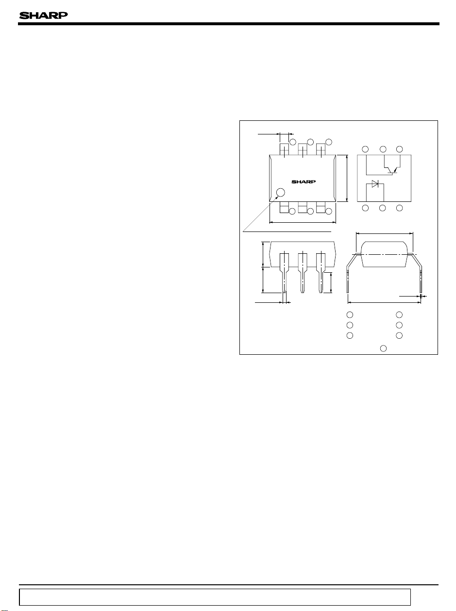
PC110L/PC111L/PC112L/PC113L
PC110L/PC111L
PC112L/PC113L
❈ Lead forming type
❈ DIN-VDE0884 approved type is also available as an option.
(
I type) and taping reel type
■ Features
1. Long creepage distance type (Creepage
distance : 8mm or more
2. Internal insulation distance : 0.5mm or
more
3. Recognized by UL(No. E64380)
Approved by VDE (DIN-VDE0884 No. 77292
Approved by BSI (BS415 : 6690, BS7002 : 7421
Approved by SEMKO
Approved by DEMKO (No. 37150
4. High collector-emitter voltage
(V
5. High isolation voltage between input and
output (V
6. Dual-in-line package
*1 Allows pin-to-pin distance minus PWB land
space to be 8mm or more.
: 70V): PC112L/PC113L
CEO
: 5 000V
iso
(
P type) are also available.
)
*1
(
PC110L ::No. 8705118
(
PC110LI / PC111LI / PC112LI / PC113LI , PC110LP0 / PC111LP0 / PC112LP0 / PC113LP0)
PC111L : No. 8705119
PC112L : No. 8705120
PC113L : No. 8705121
)
)
rms
Long Creepage
Distance Type Photocoupler
❈
Internal
connection
diagram
6
(
Unit : mm
4
5
■ Outline Dimensions
± 0.3
1.2
654
PC110
)
± 0.5
6.5
)
Anode mark (Sunken place
)
± 0.5
3.5
± 0.5
3.6
0.5
❈ PC111, PC113 have no base terminals.(6 : NC
9.22
± 0.1
)
321
± 0.5
123
± 0.3
7.62
± 0.3
3.2
1 Anode
2 Cathode
3 NC 6 Base
10.16
± 0.5
0.26
4 Emitter
5 Collector
)
)
±0.1
■ Applications
1. Switching power supplies
2. Home appliances and OA equipment for
export to Europe
3. System appliances, measuring instruments
“ In the absence of confirmation by device specification sheets, SHARP takes no responsibility for any defects that occur in equipment using any of SHARP's devices, shown in catalogs,
data books, etc. Contact SHARP in order to obtain the latest version of the device specification sheets before using any SHARP's device.”
Page 2
PC110L/PC111L/PC112L/PC113L
■ Absolute Maximum Ratings
Forward current
*2
Input
Peak forward current
Reverse Voltage V
Power dissipation P 70 mW
Collector-emitter
voltage
Emitter-collector voltage V
*3
Collector-base
Output
voltage
*3
Emitter-base voltage
Collector current I
Collector power
dissipation
Total power
dissipation
*4
Isolation voltage
Operating temperature T
Storage temperature T
*5
Soldering temperature
*2 Pulse width<=100µs, Duty ratio: 0.001
*3 Applies only to
*4 40 to 60%RH, AC for 1 minute
*5 For 10 seconds
PC110L, PC112L.
Parameter Symbol Rating Unit
PC110L/PC111L
PC112L/PC113L 70
PC110L
PC112L 70
PC110L/PC112L V
PC110L/PC111L
PC112L/PC113L 160
PC110L/PC111L
PC112L/PC113L 200
■ Electro-optical Characteristics
Parameter Symbol Conditions MIN. TYP. MAX. Unit
Input
Output
Transfer
characteristics
Forward voltage V
Reverse current I
Terminal capacitance C
Collector dark current I
Collector-emitter
PC110L/PC111L
brakedown voltage
Emitter-collector breakdown voltage
Collector-base
breakdown voltage
Current
transfer ratio
PC110L
PC112L 70 - -
PC110L
PC111L
PC112L/PC113L
Collector-emitter saturation voltage
Isolation resistance R
Floating resistance
Cut-off frequency
Rise time
Fall time
Response time
PC110L/PC111L
PC112L/PC113L
PC110L/PC111L
PC112L/PC113L
BV
BV
BV
CTR
V
(
Ta= 25˚C
I
F
I
FM
R
V
CEO
ECO
V
CBO
EBO
C
P
C
P
tot
V
iso
opr
stg
T
sol
= 20mA - 1.2 1.4 V
FIF
VR=4V - - 10 µA
R
V= 0,f= 1kHz - 30 250 pF
t
VCE= 20V, I
CEO
= 0.1mA, IF=0
CEOIC
=10µA, IF=0 6 - - V
ECOIE
= 0.1mA, IF=0
CBOIC
IF= 5mA, VCE= 5V, RBE=
I
= 10mA, VCE= 5V, RBE=
F
)
IF= 20mA, IC= 1mA, RBE=
CE(sat
DC500V, 40 to 60%RH
ISO
V= 0, f= 1MHz - 0.6 1.0 pF
C
f
f
VCE= 5V, IC= 2mA, RL= 100 Ω, - 3dB
C
t
r
V
= 2V, IC= 2mA
CE
R
= 100Ω
L
t
f
50 mA
1A
6V
35
6V
35
6V
50 mA
150
170
5 000
- 30 to + 100 ˚C
- 55 to + 125 ˚C
260 ˚C
= 0, R
F
=
BE
35 - 70 - -PC112L/PC113L
35 - -
50
50
40
5x10101x10
)
V
V
mW
mW
Vrms
--10-7A
-
100 400
0.1
-
11
- 0.2 V
- 80 - kHz
-418
-415
-318
-315
(
Ta= 25˚C
400
320
- Ω
)
V
V
%
µs
µs
PC110L/PC111L PC112L/PC113L
)
Model No.
PC110L1/PC111L1
PC110L2/PC111L2
PC110L5/PC111L5
PC110L/PC111L
CTR(%
50 to 125
100 to 250
50 to 250
50 to 400
Model No.
PC112L1/PC113L1
PC112L2/PC113L2
PC112L5/PC113L5
PC112L/PC113L
CTR(%
40 to 120
80 to 200
40 to 200
40 to 320
)
Page 3

PC110L/PC111L/PC112L/PC113L
Fig. 1 Forward Current vs. Ambient
Temperature
60
50
)
mA
(
F
40
30
20
Forward current I
0
-30100 25 50 75 100 125
)
Ambient temperature T
a
(˚C
Fig. 3 Collector Power Dissipation vs.
Ambient Temperature
200
160
150
100
PC112L
PC113L
PC110L
PC111L
50
)
mW
(
C
Collector power dissipation P
Fig. 2 Diode Power Dissipation vs.
Ambient Temperature
120
)
100
mW
(
80
70
60
40
Diode power dissipation P
20
0
- 30 12525 750
50
Ambient temperature Ta (˚C
100
)
Fig. 4 Power Dissipation vs. Ambient
Temperature
250
)
mW
(
Power dissipation P
PC112L
PC113L
200
tot
170
PC110L
150
PC111L
100
50
-3000 125
25 50 75 100
Ambient temperature T
a
(˚C
)
Fig. 5 Peak Forward Current vs. Duty Ratio
10000
5000
)
2000
mA
(
1000
FM
500
200
100
50
Peak forward current I
20
10
5
-3
5
2
10
-2 -1
5
10
Duty ratio
2
Pulse width <=100µs
Ta= 25˚C
5
2
10 1
5
0
- 30 0 25 50 75 100
Ambient temperature T
a
(˚C
)
Fig. 6 Forward Current vs. Forward Voltage
500
200
)
100
mA
(
50
F
20
10
Forward current I
T
= 75˚C
a
50˚C
5
1
020.5 1.0 1.5 2.0 2.5 3.0 3.5
Forward voltage V
25˚C
0˚C
- 25˚C
(V
F
)
Page 4

PC110L/PC111L/PC112L/PC113L
Fig. 7-a Current Transfer Ratio vs. Forward
Current
200
180
)
160
%
(
140
120
100
80
60
Current transfer ratio CTR
40
20
500kΩ
0
0.1 10 100
(
PC110L, PC111L
(
*Applies only to R
=
R
BE
100kΩ
1
Forward current IF (mA
VCE=5V
T
)
BE
= 25˚C
a
*
)
)
=
Fig. 7-b Current Transfer Ratio vs. Forward
Current
100
)
80
%
(
60
40
Current transfer ratio CTR
20
RBE=
500kΩ
0
0.1 10 100
(
PC112L, PC113L
(
*Applies only to R
100kΩ
1
Forward current I
F
(mA
V
T
BE
CE
= 25˚C
a
)
=
=5V
*
)
)
Fig. 8-a Collector Current vs. Collector- Fig. 8-b Collector Current vs. Collector-
emitter Voltage
60
50
)
mA
(
40
C
30
20
Collector current I
10
0
IF= 30mA
20mA
0
123456789
Collector-emitter voltage V
(
PC110L, PC111L
R
=
BE
T
= 25˚C
a
(
)
MAX.
P
C
10mA
5mA
)
(V
CE
)
emitter Voltage
30
25
)
20
mA
(
C
15
10
Collector current I
5
0
0
IF= 30mA
246810
Collector-emitter voltage V
(
PC112L, PC113L
R
=
BE
T
= 25˚C
a
Pc ( MAX.)
20mA
10mA
5mA
)
(V
CE
)
Fig. 9-a Relative Current Transfer Ratio vs. Fig. 9-b Relative Current Transfer Ratio vs.
Ambient Temperature
150
)
%
(
100
(
PC110L,PC111L
I
F
V
R
)(
= 5mA
=5V
CE
=
BE
Ambient Temperature
150
)
%
(
100
PC112L, PC113L
I
= 10mA
F
V
CE
R
BE
=5V
=
)
50
Relative current transfer ratio
0
- 30 0 40 60 80 100
20
Ambient temperature T Ambient temperature T
a
(˚C
50
Relative current transfer ratio
0
)
- 30 0 40 60 80 100
20
a
(˚C
)
Page 5

PC110L/PC111L/PC112L/PC113L
Fig.10-a Collector-emitter Saturation
Voltage vs. Ambient Temperature
0.16
0.14
0.12
0.10
0.08
0.06
)
sat
(
0.04
CE
V
Collector-emitter saturation voltage
0.02
0
-30
(
PC110L, PC111L
IF= 20mA
I
C
R
0 20406080100
Ambient temperature Ta (˚C
= 1mA
BE
)
)
=
Fig.11-a Collector Dark Current vs.
Ambient Temperature
-5
10
5
)
A
(
-6
10
5
CBO
,I
-7
10
CEO
5
-8
10
5
-9
10
5
-10
10
Collector dark current I
5
-11
10
- 30 0 20 40 60 100
(
PC110L, PC111L
I
CEO
V
= 20V
CE
= 30V
V
CB
Ambient temperature T
)(
= RBE=
R
BE
I
CBO
80
)
(˚C
a
Fig.12-a Response Time vs. Load Resistance
(
500
VCE=2V
I
C
200
R
100
T
50
)
µ s
(
20
10
5
2
Response time
1
= 2mA
=
BE
= 25˚C
a
PC110L, PC111L
t
f
t
r
t
d
t
s
0.5
0.2
0.1
0.01 0.1 1 10
Load resistance RL (kΩ
t
r
)
)(
t
f
50
Fig.10-b Collector-emitter Saturation
Voltage vs. Ambient Temperature
0.16
0.14
0.12
0.10
0.08
0.06
)
sat
(
0.04
CE
V
Collector-emitter saturation voltage
0.02
0
-30
(
PC112L, PC113L
I
I
R
0 20406080100
Ambient temperature Ta (˚C
= 20mA
F
= 1mA
C
BE
)
)
=
Fig.11-b Collector Dark Current vs.
Ambient Temperature
-5
10
5
)
A
(
-6
10
CBO
5
,I
-7
10
CEO
5
-8
10
5
-9
10
5
-10
10
Collector dark current I
5
-11
10
- 30 0 20 40 60 100
PC112L, PC113L
I
CEO
= 20V
V
CE
= 30V
V
CB
Ambient temperature T
a
I
(˚C
CBO
)
80
)
Fig.12-b Response Time vs. Load Resistance
500
VCE=2V
I
C
200
R
BE
100
T
a
50
)
µ s
(
20
10
5
2
Response time
1
0.5
= 2mA
=
= 25˚C
PC112L, PC113L
t
f
t
r
t
d
t
s
0.2
0.1
0.01 0.1 1 10
Load resistance RL (kΩ
t
r
t
f
)
)
50
Page 6

PC110L/PC111L/PC112L/PC113L
Test Circuit for Response Time
V
CC
Input
R
D
PC111L and PC113L PC111L and PC113L
R
L
Output
Input
Output
10%
t
t
d
t
r
90%
s
t
r
Test Circuit for Frequency Response
V
CC
R
D
R
L
have no base terminal. have no base terminal.
Fig.13-a Frequency Response Fig.13-b Frequency Response
0
)
dB
(
V
-5
-10
Voltage gain A
-15
RL= 10kΩ
(
PC110L, PC111L
100 Ω
1kΩ
V
I
R
T
CE
= 2mA
C
BE
= 25˚C
a
=5V
=
)
0
)
dB
(
V
-5
-10
Voltage gain A
-15
R
L= 10k Ω
(
PC112L, PC113L
1kΩ
Output
V
CE
I
= 2mA
C
R
BE
T
= 25˚C
a
100Ω
)
=5V
=
-20
0.2
0.5 1 2 5 10 20 50
Frequency f (kHz
100 200 500 1000
)
-20
0.2
0.5 1 2 5 10 20 50
Frequency f (kHz
100 200 500 1000
)
Fig.14-a Collector-emitter Saturation Voltage Fig.14-b Collector-emitter Saturation Voltage
vs. Forward Current
6
5
4
3
2
)
V
(
)
sat
(
1
CE
Collector-emitter saturation voltage
V
0
0
246810
●
Please refer to the chapter “ Precautions for Use”
(
PC110L, PC111L
I
= 0.5mA
C
1mA
3mA
5mA
7mA
Forward current I
F
)
Ta= 25˚C
12 14
(mA)
vs. Forward Current
6
I
5
1mA
4
3
)
2
V
(
)
sat
(
1
CE
Collector-emitter saturation voltage
V
0
0
246810
(
= 0.5mA
C
3mA
Forward current I
PC112L, PC113L
5mA
F
7mA
(mA)
T
= 25˚C
a
12 14
)
 Loading...