

Page 1

PC104-73DL1
LVDT/RVDT OUTPUT, PROGRAMMABLE
16 BIT RESOLUTION; WRAP-AROUND SELF TEST
ON-BOARD PROGRAMMABLE EXCITATION SUPPLY (OPTIONAL)
FEATURES:
• 16 bit resolution
• Continuous background bit testing and Excitation loss detection
• Transformer isolated
• No adjustments or trimming required
• Part number, S/N, Date code, & Rev. in permanent memory
DESCRIPTION:
This PC104 compliant stackthrough module offers (1) three-wire transformer isolated
“PROGRAMMABLE” LVDT/RVDT outputs with wrap-around self test and optional excitation supply.
Instead of buying cards that are set for specific outputs, the uniqueness of this design makes it
possible to buy our generic card that can be programmed and reprogrammed in the field for any
excitation and signal voltage between 2.0 and 28 volts. One transformer isolated excitation is supplied
for the A, B output pair. User selects the desired A+B voltage. After this is done, the card will
automatically set the correct B voltage for any programmed A voltage. Use of a ratiometric design
eliminates errors caused by excitation voltage variations. The outputs are stable with temperature and
switching spikes are not noticeable. To simplify logistics, Part number, S/N, Date code, & Rev. are located in
permanent memory locations.
Automatic background bit testing where the output of each channel is compared against the commanded input
to a testing accuracy of 0.1% FS and each Signal and Excitation is monitored. Any failure triggers a flag. The
testing is totally transparent to the user, requires no external programming, has no effect on the standard
operation of this card and can be enabled or disabled via the bus. The results are available in status registers.
Principal of Operation (LVDT): Typically the primary is excited by an ac source, causing a magnetic flux to be
generated within the transducer. Voltages are induced in the two secondaries, with the magnitude varying with
the position of the core. Usually, the secondaries are connected in series opposition, causing a net output
voltage of zero when the core is at the electrical center. When the core is displaced in either direction from
center the voltage increases linearly either in phase or out of phase with the excitation depending on the
direction.
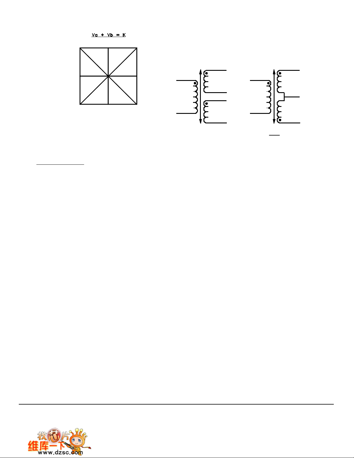
Interfacing LVDT to Converter
Two common connection methods are:
1. Primary as reference (Two-wire system)
2. Derived reference (Three/four-wire LVDT)
Two-wire system: This method of connection converts the widest range of LVDT sensors and. is the most
sensitive to excitation voltage variations, temperature and phase shift effects.
Three/four-wire LVDT: The LVDT is again excited from the primary side, but the converter reference is the
sum of A + B that has constant amplitude for changing core displacement This system is insensitive to
temperature effects, phase shifts and oscillator instability and solves the identity (A-B)/(A+B)
Apex Signal, A Division of NAI, Inc.
Bohemia, NY 11716 USA Model PC104-73DL1 Specifications PC104-73DL1 Rev D
www.naii.com Code: 0VGU1 Sheet 1 of 4
Page 2
(USUAL LVDT CONFIGURATION)
10.0 V
(IN-PHASE)
POSITION
Vb
5.0 V
Va
0.0 V
0% 50%
Va+Vb=10V
Va-Vb=-10V
Va=0V
Vb=10V
EXAMPLE USES A 10.0 Vrms OUTPUT
Va+Vb=10V
Va-Vb=0V
Va=5V
Vb=5V
100%
Va+Vb=10V
Va-Vb=10V
Va=10V
Vb=0V
EXCITATION
4 WIRE
3 WIRE
A
B
EXCITATION
A
B
A-B
A+B
SPECIFICATIONS:
Resolution: 16 bits (.001526% FS)
Linearity: 1 mV + .05% reading
Offset: 1 mV
Output Format: 3-wire or 4-wire. Transformer isolated.
Output Voltage: 2.0 to 28 Vrms ± 1% at no load, programmable with TR.
Transformer isolated. Output voltage will vary directly with excitation.
Load: With output voltages from 2.0 to 7.0 Vrms: 2.5 kΩ min.
With output voltages from 7.1 to 20.0 Vrms: 10 kΩ min.
With output voltages from 10.1 to 28.0 Vrms: 15 kΩ min. Short circuit protected.
Regulation: 1% max.
Excitation: 2.0-28 Vrms, programmable, 0.1 V resolution. Transformer isolated. (250 Mw)
Frequency: 360 Hz to 10 Khz, broadband.
Phase Shift (input to output): 0.1° max.
Excitation Z in: 50 KΩ min.
Power: +5 VDC ±5% at 0.35 A
±12 VDC ±5% at 0.5 A
Temperature: -40°C to +80 °C
Storage temperature: -55°C to +105°C.
Size: 3.6 x 3.8 x 0.6
Weight: 12 oz.
Output voltage: Output A= REF*TR* (POSITION / 65536)
Output B= REF*TR* 1- (POSITION / 65536)
Transformation Ratio (TR): [(Output A + Output B) / REF) * 65536
Apex Signal, A Division of NAI, Inc.
Bohemia, NY 11716 USA Model PC104-73DL1 Specifications PC104-73DL1 Rev D
www.naii.com Code: 0VGU1 Sheet 2 of 4
Page 3

PROGRAMMING INSTRUCTIONS:
00
Position Lo read/write
07
Freq. Out Hi write/read
0D
Model Number Hi read
15
Rev level Hi read
01
Position Hi read/write
08
Excitation. Lo write/read
10
Serial Number Lo read
16
Status, Signal read
02
Wrap-around Lo read/write
09
Excitation Hi write/read
11
Serial Number Lo read
18
Status, Excitation read
03
Wrap-around Hi read/write
0A
TR Lo write/read
12
Date Code Lo read
04
Status, Accuracy read
0B
TR Hi write/read
13
Date Code Hi read
06
Freq. Out Lo write/read
0C
Model Number Lo read
14
Rev level Lo read
Examples of voltage programming
256
128643216842128.1 Vrms entered as 281
100011001
7.0 Vrms entered as 70
001000110
I/O CONFIGURATION:
This card requires 32 consecutive addresses in the I/O address space on a 32 byte boundary. The base address is switch
settable in the 000-3E0 hex (0 to 992) address range.
ADDRESS= BASE + OFFSET
BASE A9 A8 A7 A6 A5 OFFSET A4 A3 A2 A1 A0 Decimal equiv.
SW5 ∗
SW4 ∗
SW3 ∗ 128
SW2 ∗
SW1 ∗
∗ “1” = Off “0” = On
32
64
256
512
NOTE: Base addresses to avoid:
320-32F Hard Disk 3B0-3BF Monochrome Display 3F8-3FF Asynch Comm I/O
378-37F Parallel Printer Port 3F0-3F7 Floppy Disk
Offset
Hi byte Lo byte
D15 D14 D13 D12 D11 D10 D9 D8 D7 D6 D5 D4 D3 D2 D1 D0
Data, max. 1 1 1 1 1 1 1 1 1 1 1 1 1 1 1 1
Data, 1/2 scale, max. 1 1 0 0 0 0 0 0 0 0 0 0 0 0 0 0
Data, zero 1 0 0 0 0 0 0 0 0 0 0 0 0 0 0 0
Data, 1/2 scale, min. 0 1 0 0 0 0 0 0 0 0 0 0 0 0 0 0
Data, min. 0 0 0 0 0 0 0 0 0 0 0 0 0 0 0 0
Status, Signal X X X X X X X X X X X X X X B A
Status, Excitation X X X X X X X X X X X X X X X D
Status, Test X X X X X X X X X X X X X X X D
Codes are in 2's complement.
Apex Signal, A Division of NAI, Inc.
Bohemia, NY 11716 USA Model PC104-73DL1 Specifications PC104-73DL1 Rev D
www.naii.com Code: 0VGU1 Sheet 3 of 4
Page 4

PROGRAMMING INSTRUCTIONS:
•••
•
•••
•
Power ON: sets all outputs to zero, optional excitation supply to 360 Hz and no output.
Wrap around: Can be read at any time and indicates the actual output. Read the Hi byte first. Hi byte read holds Lo byte
until read.
Optional Excitation Supply: For frequency, write a 16 bit word (Ex: 400 Hz = 110010000) to 06h/07h. For voltage,
write a 16 bit word (Ex: 26.1 Vrms =100000101) with Lsb=0.1 Vrms, to 08h/09h. It is recommended that user program the
required frequency before setting the output voltage.
To read status: Read 18h for excitation, 16h for Signal, 04h for accuracy. Test: “1” Accuracy OK; “0” failed; Status: “1”
Exc. On, Signal On. “0” Exc. and/or Signal loss.
CONNECTOR: Samtec TSW-104-25-T-D-R-A Mate: IDC 4x2 .1” Pin numbers
Pin Lo Hi Exc. Hi (In) Exc. Lo (In) Exc. Hi Out) Exc. Lo (Out) 7 5 3 1
Ch.A 1 4 7 8 5 6
Ch.B 3 2
8 6 4 2
Facing pins
PART NUMBER DESIGNATION
73DL1- 1 X X X X
Options
0 = none
9 = custom (see separate spec)
Reference Supply
R = On-board
BUS
1 = 8-bit ISA bus
2 = 16-bit ISA bus
Environmental
C = No conformal coating
K = Removable conformal coating
L = Permanent conformal coating
Total number Channels
Apex Signal, A Division of NAI, Inc.
Bohemia, NY 11716 USA Model PC104-73DL1 Specifications PC104-73DL1 Rev D
www.naii.com Code: 0VGU1 Sheet 4 of 4
 Loading...