

Page 1
PBL 388 12
1
October 1999
PBL 388 12
Voice-switch circuit for
Handsfree speakerphone TAM
Description
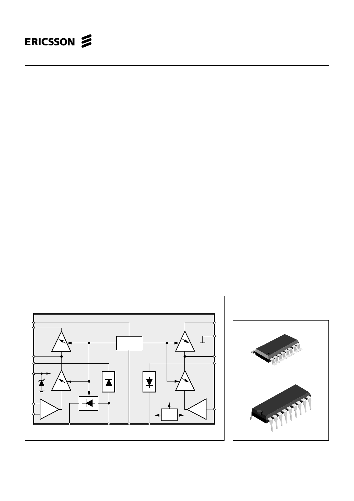
The PBL 388 12 contains all the necessary circuitry , amplifiers, detectors, comparators
and control functions to implement a high performance, voice-switched, ”hands-free ”
function in an answering machine. The gain dynamics (attenuation between channels)
is settable (25dB or 50dB) via CTR pin that also control two mute levels. A background
noise detector in the transmitting channel reduces the influence of continuous noise signals.
The PBL 388 12 is designed for answering machines that are either powered from the
telephone line or from a mains powered dc. supply.
Filtering of both the audio and control signals in both transmitter and receiver channels
possible.
An external loudspeaker amplifier has to be used, normally the same as used for the
answering machine.
Control
F2
F3
F6
F5
F1
PBL 388 12
F4
4
2
3
879
10
14
12
1
5
16
+
+
–
+
11
13
Ref.
6
15
PBL388 12
16-pin SO
Figure 1. Block diagram. ( SO - package )
18-pin DIP
PBL388 12
Key Features
• Settable gain dynamics (25 or 50
dB).
• Low power consumption, totally
1.0mA at 3.3V typical.
• Background noise compensation in
the transmitting channel with hold
function.
• Exellent noise performance.
• Both channel input amplifiers have
balanced inputs.
• Minimum of external components
needed for function.
• 16-pin SO and 18-pin DIP
encapsulation.
All figures in this paper refer to 16-pin SO package.
Page 2
PBL 388 12
2
Maximum Ratings
Parameter Symbol Min Max Unit
Speech switch supply current I
D
10 mA
Voltage pin 1-14 -0,5 Vpin
15
+0.5 V
Operating temperature T
Amb
-20 +70 °C
Storage temperature T
Stg
-55 +125 °C
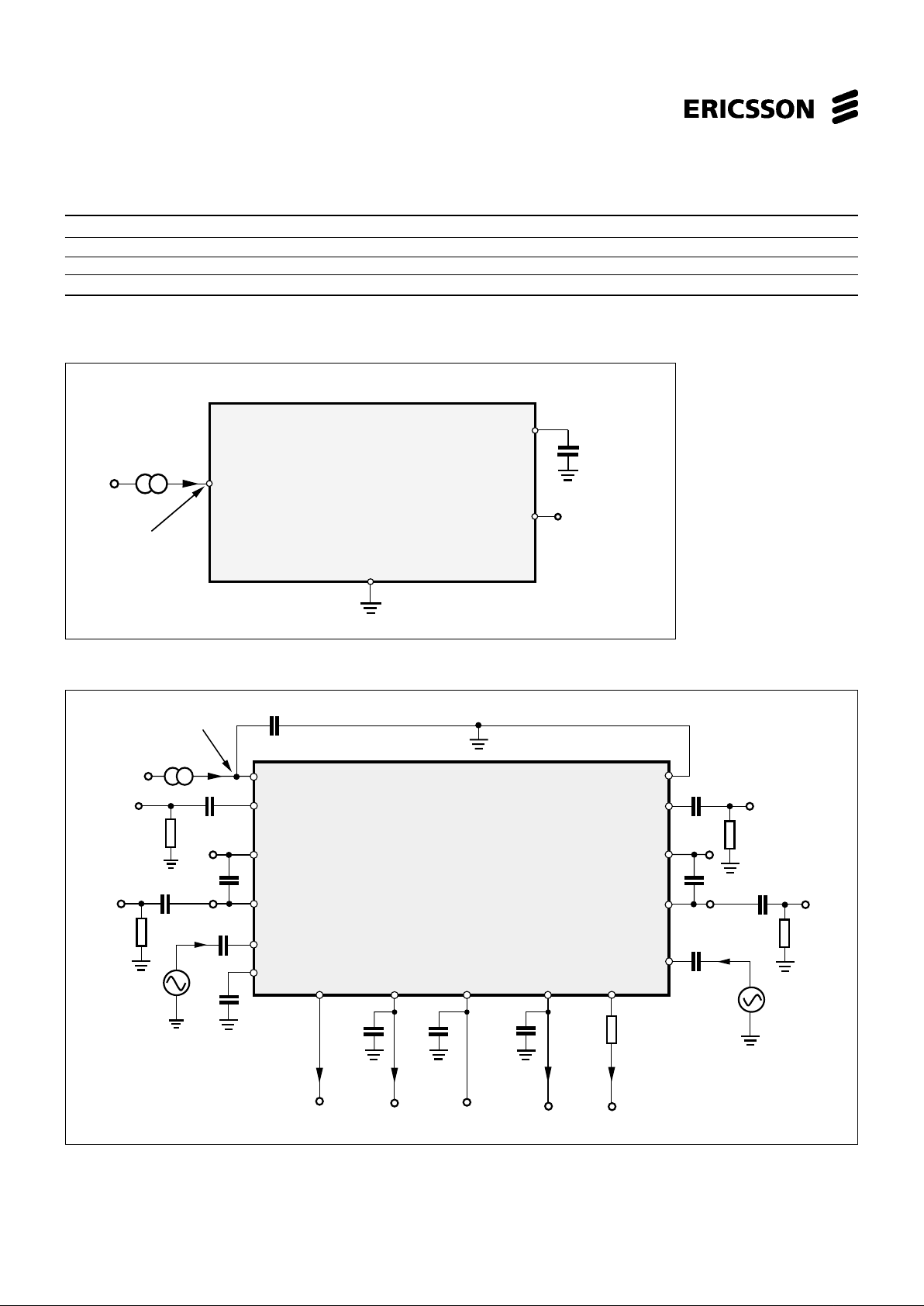
Figure 3. T est circuit. Reference figure No. 3.
Figure 2. Isolation and measurement of V
Ref
. Reference figure No.2.
CTR
V
V
CMP
V
TxDet
V
Rxout
CMP CTR
GND
79
10
1
16
8
Det
N
Tx
Detout
5
Tx
out
Rx
Detout
3
1 µF
Rxin
I
V
Rxin
+
NDet
R
CTR
C
TxDet
I
TxDet
0,1µF
C
RxDet
V
RxDet
I
CTR
V
NDet
RxDet
I
PBL 388 12
12
Rx
out
R
Rxout
10 µF
+
2
4
6
F2
out
14
100µF/16V
V
+
15
V
+
+
+
Tx
Detin
-Tx
in
+Tx
in
in
-Rx
11
Rx
Detin
13
F5
out
10 µF
+
F5
out
R
F5
out
C
Rx
V
Txout
+
10 µF
Txout
R
+
D
I
I
Txin
V
Txin
4.7 µF
+
1 µF
+
10 µF
+
F2
out
R
F2
out
C
Tx
+
V
+
GND
V
Ref
+
PBL 388 12
V
+
D
I
RxDetin
RxDetout 10
15
16
11
100nF
Page 3

PBL 388 12
3
Electrical Characteristics
f = 1 kHz, T = 25°C, R
CTR
=0, C
TxDet
= 0, R
Txout
= ∞, R
Rxout
= ∞, R
F2out
= ∞, R
F5out
= ∞, RTx= 0, RRx= 0, C
RxDet
= 0 and
I
D
=1.0mA unless otherwise noted.
Ref.
Parameter fig. Condition Min. T yp. Max. Unit.
Speech control section
T erminal voltage, V
+
3ID = 1.0mA 3.3 V
Internal reference voltage, V
Ref
2 1.96 V
Frequency response for all amplifiers 3 200 - 3400 Hz, Relative 1 kHz -1 1 dB
Transmit gain, 20 •
10
log(V
Txout
/V
Txin
)3V
CMP
= V
Ref
- 0.1 V 41.5 44 dB
V
CMP
= V
Ref
+ 0.1 V -6 -3.5 dB
V
CMP
= V
Ref
- 0.1 V R
CTR
=100k, V
CTR
=V+ 41.5 44 dB
V
CMP
= V
Ref
+ 0.1 V R
CTR
=100k, V
CTR
=V+ 19 21.5 dB
Receive gain, 20 •
10
log(V
Rxout
/V
Rxin
)3V
CMP
= V
Ref
+ 0.1 V 26.5 29 dB
V
CMP
= V
Ref
- 0.1 V -21 -18.5 dB
V
CMP
= V
Ref
+ 0.1 V R
CTR
=100k, V
CTR
=V+ 26.5 29 dB
V
CMP
= V
Ref
- 0.1 V R
CTR
=100k, V
CTR
=V+ 4 6.5 dB
Max transmit detector gain, 3 V
TxDet
< 200 mVp , CTx = 100nF
20 •
10
log(V
Txdet
/V
Txin
)V
CMP
= V
Ref
- 0.1 V 67.5 dB
V
CMP
= V
Ref
+ 0.1 V 37 42.5 dB
Max receive detector gain, 3 V
RxDet
< 200 mVp , CTx = 100nF
20 •
10
log(V
Rxdet
/V
Rxin
)V
CMP
= V
Ref
+0.1 V 53 dB
V
CMP
= V
Ref
- 0.1 V 22.5 28 dB
Background noise rectifier gain, (note 1) 3 V
CMP
= V
Ref
- 0.1 V , C
Txdet
=1µF 6.0 dB
V
CMP
= V
Ref
+ 0.1 V , C
Txdet
=1µF Hold
+ Tx
In
input impedance 3 80 100 120 kΩ
- Tx
In
input impedance 3 2.4 3.0 3.6 kΩ
- Rx
In
input impedance 3 16 20 24 kΩ
Tx
Out
ac, load impedance 3 10 kΩ
Rx
Out
ac, load impedance 3 10 kΩ
F2
Out
ac, load impedance 3 10 kΩ
F5
Out
ac, load impedance 3 10 kΩ
Transmitter channel output swing, v
TxOut
3 2% distortion,R
Txout=RRxout
=25k Ω 500 mV
p
Receiver channel output swing, v
RxOut
3 2% distortion,R
Txout=RRxout
=25k Ω 500 mV
p
Transmitter output noise, v
TxOut
3V
CMP
= V
Ref
- 0.1 V , v
TxIn
= 0 V -75 dB
psof
Receiver output noise, v
RxOut
3V
CMP
= V
Ref
+ 0.1 V , v
RxIn
= 0 V -75 dB
A
Tx
Det
sink current, I
TxDetOut
3V
TxDetIn
= V
Ref
+ 0.1 V -6.0 -2.5 mA
Rx
Det
source current, I
RxDetOut
3V
RxIn
= V
Ref
- 0.1 V 2.5 6.0 mA
Tx
Det
source current, I
TxDet
3V
CMP
= V
Ref
- 0.1 V 30 µA
Rx
Det
sink current, I
RxDetOut
3V
RxDetIn
= V
Ref
+ 0.1 V -30 µA
Tx
Det
swing relative to V
Ref
, V
TxDetOut
3V
TxDetIn
= V
Ref
+ 0.1 V (note 2) -0.7 V
Rx
Det
swing relative to V
Ref
, V
RxDetOut
3V
RxDetIn
= V
Ref
- 0.1 V (note 2) +0.7 V
N
Det
sink current (fast charge), I
NDet
3V
TxDetIn
= V
Ref
- 0.1 V -4.5 -1.5 mA
V
CMP
= V
Ref
- 0.1 V
N
Det
source current, I
NDet
3V
TxDetIn
= V
Ref
+ 0.1 V 3 5 7 µA
V
CMP
= V
Ref
+ 0.1 V
Page 4

PBL 388 12
4
Ref.
Parameter fig. Conditions Min. Typ. Max. Unit.
N
Det
leakage current (hold), I
NDet
3V
TxDetIn
= V
Ref
- 0.1 V , -100 nA
V
CMP
= V
Ref
+ 0.1 V ,
N
Det
swing relative to V
Ref
, V
NDet
3V
CMP
= V
Ref
- 0.1 V, -0.45 V
V
TxDetIn
= V
Ref
+ 0.1 V
CMP (comparator) sensitivity, 3 Tx mode = max Tx gain, 50 100 mV
transmit (Tx) mode to receive 13 Rx mode = max Rx gain
(Rx) mode or vice versa
CTR voltage for 25 dB dynamics, V
CTR
3V
CMP
= V
Ref
± 0.35 V , R
CTR
=100kΩ V
+
V
CTR voltage for mute, I
CTR
3V
CMP
= V
Ref
± 0.35 V µA
CTR voltage for disable, V
CTR
3 0.55 V
Notes:
V
NDet
- V
Ref
1. 20 •
10
log ( )
V
TxDet
- V
TxDetO
V
NDet
= voltage at noise detector output
V
Ref
= reference voltage (about 1.9 V) see figure 2.
V
TxDet
= Voltage at transmit detector output.
V
TxDetO
= voltage at transmit detector output at the point
when the voltage at the noise detector starts
moving when a signal at transmit channel input is
gradually increased (threshold, typical value 30 mV)
2. Depends on V
+
. Channels are tracking.
Page 5

PBL 388 12
5
Figure 4. Pin configuration.
Pin Descriptions:
Refer to figure 4. (16-pin SO and 18-pin DIP package)
16-pin SO
SO DIP Symbol Description
1 16 CTR Control input for gain dynamics
(25 or 50dB), mute and disable.
2 17 -Txin Transmitter channel negative input.
Input impedance 3 kohm.
3 18 +Txin Transmitter channel positive input.
Input impedance 100 kohm.
4 1 F2out Output of the second amplifier in the
transmitter channel.
5 2 Txout Transmitter channel output. Min. ac
load impedance 10 kohm.
6 3 TxDetin Input of the transmitter channel signal
detector. Input impedance 13 kohm.
7 4 TxDetout Output of the transmitter channel signal
detector. Goes nagative referred to the
internal ref. voltage of app. 2V when a
transmitter signal is present.
8 5 NDet Background noise detector output.
Goes positive referred to the internal ref.
voltage of app. 2V when a backgrounud
noise signal is present
SO DIP Symbol Description
9 6 CMP Comparator input..
Summing point to the different
detector outputs.
10 7 RxDetout Output of the receiver channel signal
detector. Goes positive referred to the
internal ref. voltage of app. 2V when a
receiver signal is present
11 8 RxDetin Input of the receiver channel signal
detector. Input impedance 13 kohm.
12 9 Rxout Receiver channel output. Min. ac load
impedance 10 kohm.
13 10 F5out Output of the second amplifier in the
receiver channel.
11 +Rxin Receiver channel positive input. Input
impedance 140 kohm.
14 12 -Rxin Receiver channel negative input. Input
impedance 20 kohm.
15 13 V+ Supply of the speech switching
circuitry . Ashunt regulator, voltage
apprx. 3.3V at 1.0mA.
16 14 GND System ground.
15 NC Not connected.
18-pin DIP
Pin Pin Pin Pin
F2out
Txout
TxDetin
TxDetout
N Det
CMP
RxDetout
Rx Detin
CTR
NC
GND
+V
-Rxin
+Rxin
1
2
3
4
5
6
7
8
16
15
14
13
12
11
F5out
9 10
+Txin
-Txin
18
17
Rxout
1
2
3
4
5
6
7
8
16
15
14
13
-Txin
CTR
NDet
F2out
+V
RxDetout
+Txin
TxDetin
-Rxin
Rxout
CMP
9
12
10
11
F5out
GND
TxDetout
RxDetin
Txout
Page 6

PBL 388 12
6
Figure 6. Receiver and transmitter channel input arrangement.
Figure 5. Passive networks setting the speech control function.
Functional Description
Speech control section
Transmitter and Receiver
Channels
The transmitter and receiver channels
consist of three amplifying stages each,
F1, F2, F3 and F4, F5, F6. The inputs of
the amplifiers must be ac. coupled
because they are dc. vise at the internal
reference voltage (≈2V) level. F1 and F4
are fixed gain amplifiers of 30,5 dB and
15.5 dB respectively, while the rest of them
are of controlled gain type.The gain of F2,
F3 as well as F5 and F6 is controlled by
comparators. The comparator receives its
information partly from the summing point
of the transmitter, receiver and background noise detectors at CMP input and
partly through the control input, CTR,
which controls the gain dynamics (25 or
50 dB). Amplifiers F2 and F3 have the
maximum gain when the transmitter
channel is fully open, consequently the
amplifiers F5 and F6 will have minimum
gain and vice versa. See figure 5 and figure
11.
The positive input on transmitter and the
negative input on receiver channel has a
rather high input impedance. It renders a
good gain precision and noise
performance when used with low signal
source impedance. The differential input
of the transmitter channel can be used to
suppress unwanted signals in the
microphone supply, see figure 7. Also see
application 1.
Signal Detectors and
Comparator
The signal detectors sense and rectify
the receiver and microphone signals to
opposite polarities referenced to the
internal reference voltage of approx. 2V .
The voltage at RxDet will go positive and
at TxDet negative in the presence of a
signal at the respective channel input. In
the idle (no signal) state, the voltages at
RxDet ,TxDet and CMP are equal to the
internal reference voltage. Signal at Txin
will result in an decreasing level at
TxDetout and hence also at CMP input.
R5
C3 C1 C2
C4
F2
F3
F1
PBL 388 12
1
5
15
4
2
3
87
9
10
+
-
+
CTR
CMP
V
+
N
Det
R
xout
R
xin
T
xDet
R
xDet
-T
xin
+
T
xin
T
xout
12
14
F6
F5
Control
F4
+
Ref.
13
11
6
GND
16
+
+
F
1
F
4
2
3
14
F
5
++
F
2
V
Rxin
V
Txin
100k3k100k
120k
120k
20k
Tx
Ref.
I
~
16
3k
PBL388 12
~
Rx
Page 7

PBL 388 12
7
Figure 7. Transmitter channel input
amplifier used to suppress ripple in the
mic. supply. (CMRR).
R1 = R2
≈
3k
R3 = R4
≈
100k
R5 = R6
C1 = C2
Figure 8. T ransmitter and receiver
channel rectifier characteristics.
Figure 10. Transmitter and receiver
channel output dynamics.
Figure 9. Relationship in timing between
the voltage levels at Tx
In
, Tx
Det
and N
Det
0.5 1.0
1.5
V
Rx in
10
V
TxDet
≈ 2V
V
ref
-600
-400
-200
+600
+200
+400
V
ref
2.5
5.0
7.5
V
Tx in
RxDet
V
m
V
p
Txin
TxDetout
N
Det
F
1
2
3
-
+
F
2
R4
R2
R3
Ref.
R1
R6
R5
C2
C1
C3 C4
R7
16
Mic.
+
V+ (V)
V
(mV)
Txout
2.4 2.6
2.8 3.0 3.2
3.4
100
200
300
400
500
≈
2.4 2.6
2.8 3.0 3.2
3.4
V+ (V)
100
200
300
400
500
V
R
(mV)
xout
≈
Page 8

PBL 388 12
8
Figure 13. Control modes as function of voltage applied to gain dynamics control
input CTR; I
D
=1mA.
Figure 11. Transmit and receive gain as a function of V
CMP
and V
CTR
.
Figure 12. Timing of the transmitter and receiver channels at the CMP-input.
the transmitter channel and decrease it in
the receiver channel. Signal at Rxin will
do vice versa. The voltages RxDetout and
TxDetout control thus the gain setting in
respective channel through the
comparators using the CMP input as a
summing point with an input current of
less than 1µA. The attack and decay times
for the signals RxDetout and TxDetout are
controlled by individual external RCnetworks. The attack time in the receiver
channel is set by C2 together with C1 and
either by the maximum current capability
of the detector output or it with R2 added.
The transmitter channel works likewise.
See fig. 7.
The decay time in the receiver and transmitter channels is set by C2 and C3
respectively. The resistor in the time constant is formed by an internal 200kΩ resistor
in parallel with the external resistors R3
and R4 respectively. The influence of
eventual R1 and R2 can be omitted.
The text above describes the case when
only one channel is open at a time and
there is a distinctive pause between signals at receiver and transmitter channel
inputs so the circuit will have time to reach
its idle state. See fig.14 A) to E). If one of
the channels gets an input signal
immediately after the signal has
disappeared from the other channel input
the effective decay time, as the CMP input sees it, will be shorter than in the first
case. See fig.14 F) to G). The capacitor
C4 at CMP - input sets the speed of the
gain change in the transmitter and receiver channels. The capacitors C2 and C3
should be dimensioned for a charging time
of 0.5 - 10mS and for a discharge time of
150 - 300 mS. The question of switching
times being a highly subjective proposition, is in large dependent of the language
being spoken in the system, caused by
the varying sound pressure picture of the
different languagues. A hysteresis effect
is achieved in the switching since the level
detectors sense the signals after F2 and
F5 respectively (F2 and F5 are affected
by the gain setting). For example: If the
transmitter channel is open (maximum
gain), a smaller signal at Txin is enough
to keep the channel open than would
benecessary to open it when the receiver
channel is open. The output swing of the
level detectors is matched for variations in
the supply voltage. The detectors have
Transmit
gain =
Receive
gain =
dB
dB
40
30
20
10
0
-40-60 -20 0
20 40 60
V -V
CMP
REF
____
30
20
10
0
-10
-20
mV
---------
V
CTR
REF
= V
VCTR=V+
VCTR=open
VCTR=V+
VCTR=open
1
23
0
Total mute
Mode
V
CTR
(V)
V
ref
DTMFMute
50 dB speech
control
25 dB speech
control
Full transmit level
Full recieve level
Rxdet
Txdet
CMP
B
D
E
F
G
C
A
Page 9

PBL 388 12
9
a logarithmic rectifier characteristic
whereby gain and sensitivity is high at
small signals. There is a break point in the
curve at a level of ± 200mV from the
internal reference voltage app. 2V, where
the sensitivity for increasing input signals
decreases with factor of 10, increasing the
detectors dynamic range. See fig.10.
Background Noise Detector
The general function of the background
noise detector in the transmittng channel
is to create a positive signal ( in respect to
the referrence) so that, when coupled to
the summing point at the CMP input, will
counteract the signal from the transmitter
level detector representing the actual
sound pressure level at the microphone.
This counteracts the noise from
influencing the switching characteristics.
The input signal to the backround noise
level detector is taken from the output of
the transmitter detector , a voltage
representing the envelope of the amplified
microphone signal. The detector inverts
and amplifies this signal 2 x (transmitting
mode) and has on it´s output a RC network
consisting of an internal resistor of 100k
and an external capacitor C4. The voltage
across C4 is connected to the CMP input
(summing point) via a resistor R5. The
resistor R6 is important in order to keep
the charging current of C4 within safe limits
in regard of high charge peaks that could
be audible in the system.. The extent to
which the NDet output will influence the
potential at CMP input is set by the gain of
the detector, the maximum swing and R5.
If a continuous input signal is received from
the microphone ( > 10sec.) the voltage
across C4 is pulled negative (relative to
the reference) with a time constant set by
C4 to e.g. 5 sec.. A continuous input signal is thus treated as noise. Since the output of the noise detector is going negative
it thereby counteracts the signal from the
transmitter detector and thus helping the
receiver detector signal to maintain a set
relation to the transmitter detector signal.
If the transmitter input signal contains
breaks like breath pauses the voltage at
TxDetout decreases. If the voltage across
C3 gets less than the inverted voltage
across C4 divided by the detector gain a
rapid charge of C4 towards reference will
follow (all levels referred to the reference).
If the breaks are frequent as in speech the
background detector will not influence the
switching characteristic of the system. See
fig. 11. There is a threshold of approx.
50mV at TxDetout to prevent the activation
of background noise detection in noiseless
environment. In the receiver mode some
of the loudspeaker output signal will be
sensed by the microphone. In order not to
treat this input signal as noise, the noise
detector goes into a hold state and
”remembers” the level from the previous
transmitting mode periode.
CTR Input
For full speech control (50dB attenuation
between the channels) this input can be
left unconnected. To set the function to
25dB attenuation the input has to be higher
than 600mV below V+. See figure 13. To
set the circuit into a mute state (results in,
redeced gain in receiver channel for the
DTMF confidence tone in the loudspeaker
and closed transmitter channel) a voltage
below Vref has to be connected to the input. By lowering the voltage at the input
below 0.9V a condition will emerge where
both receiver and transmitter channels are
closed. See fig. 11 and 15.
Control
F2
F3
F5
F4
F1
PBL 388 12
Power amplifier
input
P1
C
12
16
14
C
C
R
8
7
9
10
CMP
R5
C2
C1
C3
C4
+
Transmitter
channel output
R
C
CTR
1
5
15
+
6
4
2
3
+L
R
+
C
R
C
R
C
C
C
+
GND
Receiver
input
Rx
in
N
Det
Tx
Det
Rx
Det
R
Rx
out
+
Tx
out
Tx
in
+
Mic.
F6
Tx
in
13
11
Ref.
+
+
Figure 14. Speech switching arrangement.
Page 10

PBL 388 12
10
Ericsson Components AB
S-164 81 Kista-Stockholm, Sweden
Telephone: (08) 757 50 00
Specifications subject to change without
notice.
1522-PBL 388 12/1 Uen Rev.A
October 1999
© Ericsson Components AB,
Information given in this data sheet is believed to be
accurate and reliable. However no responsibility is
assumed for the consequences of its use nor for any
infringement of patents or other rights of third parties
which may result from its use. No license is granted
by implication or otherwise under any patent or patent
rights of Ericsson Components AB. These products
are sold only according to Ericsson Components AB'
general conditions of sale, unless otherwise confirmed
in writing.
Ordering Information
Package Temp. Range Part No.
Plastic SO -20 to 70°C PBL 388 12/1SO
Plastic SO -20 to 70°C PBL 388 12/1SO:T (Tape and Reel)
Plastic DIP -20 to 70°C PBL 388 12
+
15
+V
I
D=1mA
PBL
388 12
The circuit has a buit in shunt voltage
generator. It needs a minimum 1 mA
current for its function. The voltage at this
current will be 3.3V. If the voltage +V is not
constant care must be taken so that the I
D
will not exeed 10 mA.
Figure 15. Circuit supply function.
 Loading...