

Page 1
Description
The PBL 386 61/2 Subscriber Line Interface Circuit (SLIC) is a 90 V bipolar integrated
circuit for use in Central Office, MUX and other telecommunications equipment. The
PBL 386 61/2 has been optimized for low total line interface cost and a high degree of
flexibility in different applications.
The PBL 386 61/2 emulates a transformer equivalent dc-feed, programmable
between 2x25 Ω and 2x900 Ω, with short loop current limiting adjustable to max
65 mA.
A second lower battery voltage may be connected to the device to reduce short
loop power dissipation. The SLIC automatically switches between the two battery
supply voltages without need for external components or external control.
The SLIC incorporates loop current and ring trip detection functions. The
PBL 386 61/2 is compatible with loop start signalling.
Two- to four-wire and four- to two-wire voice frequency (vf) signal conversion is
accomplished by the SLIC in conjunction with either a conventional CODEC/filter or
with a programmable CODEC/filter, e.g. SLAC, SiCoFi, Combo II. The programmable
line terminating impedance could be complex or real to fit every market.
Longitudinal line voltages are suppressed by a feedback loop in the SLIC and the
longitudinal balance specifications meet Bellcore TR909 requirements.
The PBL 386 61/2 package is 28-pin PLCC.
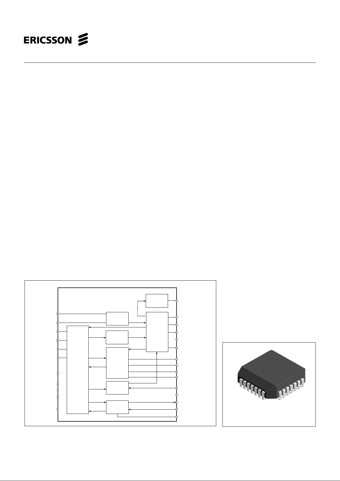
Figure 1. Block diagram.
February 2000
PBL 386 61/2
Subscriber Line
Interface Circuit
28-pin plastic PLCC
VF Signal
Transmission
Off-hook
Detector
Line Feed
Controller
and
Longitudinal
Signal
Suppression
Ring Trip
Two-wire
Interface
Input
Decoder and
Control
C1
C2
DET
REF
LP
VTX
RSN
DT
DR
TIPX
HP
RINGX
VCC
VEE
VBAT2
VBAT
AGND
C3
BGND
Comparator
Ground Key
Detector
Ring Relay
Driver
RRLY
PLD
PLC
PSGTS
AOV
VEE
PBL
386 61/2
Preliminary
Key Features
• Selectable overhead voltage principle
– All adaptive: The overhead voltage
follows 0.6 V
Peak
< signals < 6.2 V
Peak
.
– Semi adaptive: The overhead voltage
follows 3.1 V
Peak
< signals < 6.2 V
Peak
.
• Metering 2.2 V
rms
.
• High and low battery with automatic
switching
• Battery supply as low as -10 V
• Only +5 V in addition to GND
and battery (VEE optional)
• 39 mW on-hook power dissipation in
active state
• Long loop battery feed tracks V
Bat
for
maximum line voltage
• 44 V open loop voltage @ -48 V battery
feed
• Constant loop voltage for line
leakage <5 mA
• On-hook transmission
• Full longitudinal current capability
during on-hook
• Programmable loop & ring-trip detector
threshold
• Analog temperature guard
1
Page 2

PBL 386 61/2
2
Preliminary
Maximum Ratings
Parameter Symbol Min Max Unit
Temperature, Humidity
Storage temperature range T
Stg
-55 +150 °C
Operating temperature range T
Amb
-40 +110 °C
Operating junction temperature range, Note 1 T
J
-40 +140 °C
Power supply, 0°C ≤ T
Amb
≤ +70°C
V
CC
with respect to AGND V
CC
-0.4 6.5 V
V
EE
with respect to AGND V
EE
V
Bat
0.4 V
V
Bat
with respect to BGND, continuous V
Bat
-75 0.4 V
V
Bat
with respect to BGND, 10 ms V
Bat
-80 0.4 V
V
Bat2
with respect to A/BGND V
Bat2
V
Bat2
0.4 V
Power dissipation
Continuous power dissipation at T
Amb
≤ +70 °CP
D
1.5 W
Ground
Voltage between AGND and BGND V
G
-5 VCC V
Relay Driver
Ring relay supply voltage BGND +13 V
Ring relay current 75 mA
Ring trip comparator
Input voltage V
DT
, V
DR
V
Bat
V
CC
V
Input current I
DT
, I
DR
-5 5 mA
Digital inputs, outputs (C1, C2, DET)
Input voltage V
ID
-0.4 V
CC
V
Output voltage (DET not active) V
OD
-0.4 V
CC
V
Output current (DET) I
OD
30 mA
TIPX and RINGX terminals, 0°C < T
Amb
< +70°C, V
Bat
= -50 V
TIPX or RINGX current I
TIPX
, I
RINGX
-110 +110 mA
TIPX or RINGX voltage, continuous (referenced to AGND), Note 2 V
TA
, V
RA
V
Bat
2V
TIPX or RINGX, pulse < 10 ms, t
Rep
> 10 s, Note 2 VTA, V
RA
V
Bat
- 20 5 V
TIPX or RINGX, pulse < 1 µs, t
Rep
> 10 s, Note 2 VTA, V
RA
V
Bat
- 40 10 V
TIP or RING, pulse < 250 ns, t
Rep
> 10 s, Note 3 VTA, V
RA
V
Bat
- 70 15 V
Recommended Operating Condition
Parameter Symbol Min Max Unit
Ambient temperature T
Amb
0 +70 °C
Maximum supplied V
CC
with respect to AGND V
CC
4.75 5.25 V
V
EE
with respect to AGND V
EE
V
Bat
-4.75 V
V
Bat
with respect to BGND V
Bat
-58 -10 V
V
Bat2
with respect to BGND V
Bat2
V
Bat
-10 V
Notes
1. The circuit includes thermal protection. Operation above max. junction temperature may degrade device reliability.
2. A diode in series with the VBat input increases the permitted continuous voltage and pulse < 10 ms to -85 V. A pulse
≤1µs is increased to the greater of |-70V| and |VBat -40V|.
3. R
F1
and RF2 ≥20 Ω are also required. Pulse is supplied to TIP and RING outside RF1 and RF2.
Page 3
PBL 386 61/2
3
Preliminary
Electrical Characteristics
0 °C ≤ T
Amb
≤ +70 °C, VCC = +5V ±5 %, VEE = -5V ± 5%, V
Bat
= -58V to -40V, RLC=18.7kΩ, IL = 27 mA, ZL = 600 Ω, RF1, RF2 = 0 Ω,
R
Ref
= 15kΩ, CHP = 68nF, CLP=0.33 µF, RT = 120 kΩ, RSG = 24 kΩ, RRX = 120 kΩ, AOV and V
Bat2
pin not connected, unless
otherwise specified. Current definition: current is positive if flowing into a pin.
Ref
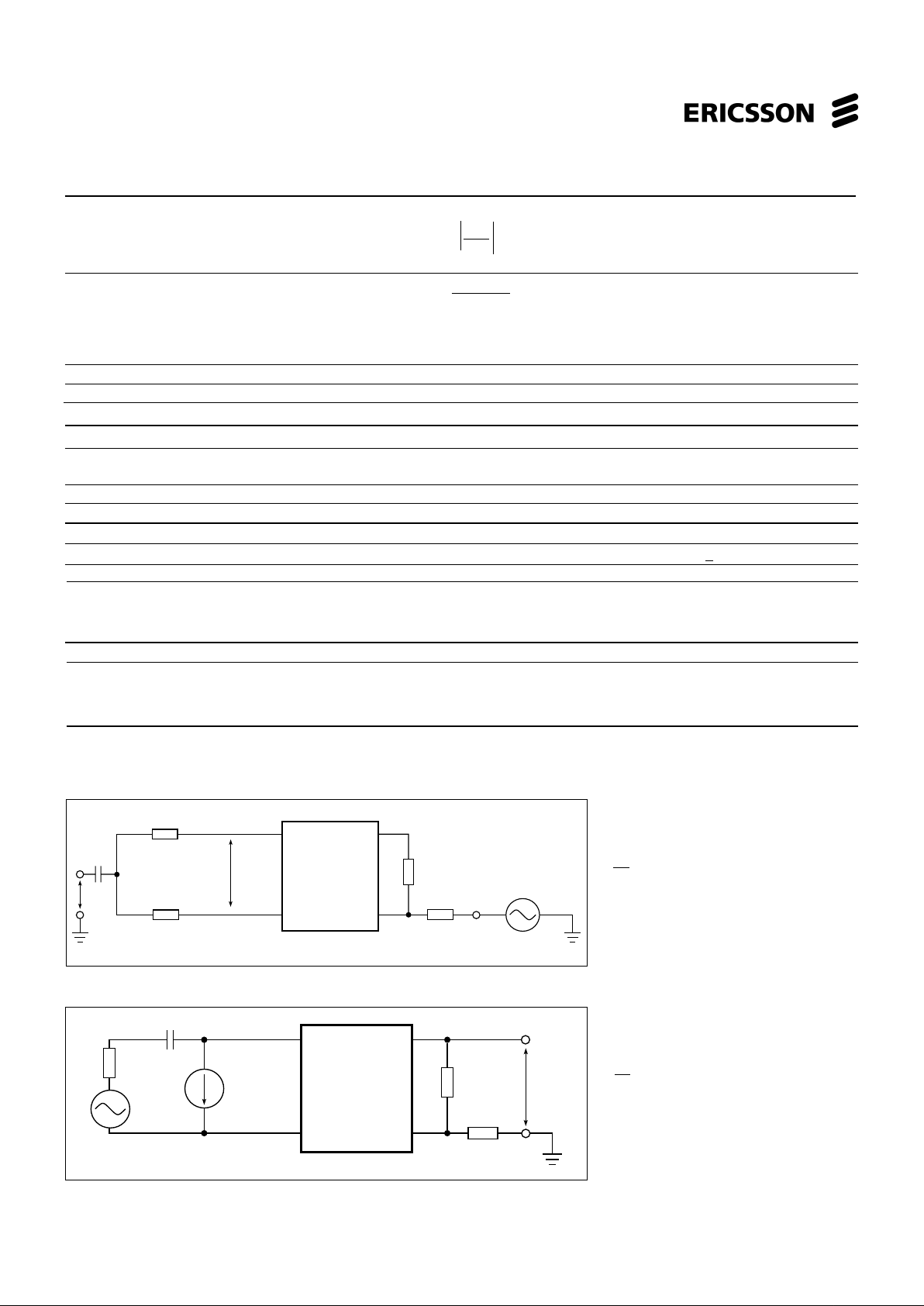
Parameter fig Conditions Min Typ Max Unit
Two-wire port
Overload level, V
TRO ,ILDC
> 10 mA 2 Active state
1% THD, Note 1 3.1 V
Peak
On-Hook, I
LDC
≤ 5 mA 1.4 V
Peak
Input impedance, Z
TR
Note 2 ZT/200
Longitudinal impedance, Z
LoT
, Z
LoR
0 < f < 100 Hz 20 35 Ω/wire
Longitudinal current limit, I
LoT
, I
LoR
active state 28 mA
rms
/wire
Longitudinal to metallic balance, B
LM
IEEE standard 455-1985, ZTRX = 736 Ω, active state
0.2 kHz < f < 1.0 kHz 55 dB
1.0 kHz < f < 3.4 kHz 55 dB
Longitudinal to metallic balance, B
LME
3 active state
E
Lo
B
LME
= 20 • Log 0.2 kHz ≤ f ≤ 1.0 kHz 55 dB
V
TR
1.0 kHz < f < 3.4 kHz 55 dB
Longitudinal to four-wire balance, B
LFE
3 active state
E
Lo
B
LFE
= 20 • Log 0.2 kHz ≤ f ≤ 1.0 kHz 61 dB
V
TX
1.0 kHz < f < 3.4 kHz 61 dB
Metallic to longitudinal balance, B
MLE
4 active state
VTR
0.2 kHz < f < 3.4kHz 40 dB
B
MLE
= 20 • Log
V
Lo
Figure 2. Overload level, V
TRO
, two-wire
port
1
<< RL, RL= 600 Ω
ωC
RT = 120 kΩ, RRX = 120 kΩ
PBL 386 61/2
TIPX
RINGX
RSN
VTX
R
T
R
RX
E
RX
R
L
V
TRO
I
LDC
C
PBL 386 61/2
TIPX
RINGX RSN
VTX
R
T
R
RX
V
TX
R
LT
C
V
TR
R
LR
E
Lo
Figure 3. Longitudinal to metallic (B
LME
)
and Longitudinal to four-wire (B
LFE
)
balance
1
<< 150 Ω, R
LR
= RLT = RL /2= 300Ω
ωC
RT = 120 kΩ, RRX = 120 kΩ
Page 4
PBL 386 61/2
4
Preliminary
Parameter fig Conditions Min Typ Max Unit
Four-wire to longitudinal balance, B
FLE
4 active state
E
RX
B
FLE
= 20 • Log
V
Lo
0.2 kHz < f < 3.4 kHz 40 dB
Two-wire return loss, r |Z
TR
+ ZL|
r = 20 • Log
|Z
TR
- ZL|
0.2 kHz < f < 0.5 kHz 25 dB
0.5 kHz < f < 1.0 kHz 27 dB
1.0 kHz < f < 3.4 kHz, Note 3 23 dB
TIPX idle voltage, V
Ti
active, IL = 0 - 1.5 V
RINGX idle voltage, V
Ri
active, IL = 0 V
Bat+
2.7 V
V
TR
active, IL = 0 V
Bat
+4.2 V
Four-wire transmit port (VTX)
Overload level, I
LDC
≥ 10 mA 5 Load impedance > 20 kΩ, 1.55 V
Peak
On hook I
LDC
≤ 5 mA 1% THD, Note 4 0.7 V
Peak
Output offset voltage, ∆V
TX
-60 60 mV
Output impedance, z
TX
0.2 kHz < f < 3.4 kHz 5 20 Ω
Four-wire receive port (RSN)
Receive summing node (RSN) dc voltage I
RSN
= 0 mA GND +25 mV
Receive summing node (RSN) impedance 0.2 kHz < f < 3.4 kHz 10 50 Ω
Receive summing node (RSN) 0.3 kHz < f < 3.4 kHz
current (I
RSN
) to metallic loop current (IL) 400 ratio
gain,α
RSN
Frequency response
Two-wire to four-wire, g
2-4
6 relative to 0 dBm, 1.0 kHz. ERX = 0 V
0.3 kHz < f < 3.4 kHz -0.15 0.15 dB
f = 8.0 kHz, 12 kHz, 16 kHz -0.5 -0.1 0 dB
Figure 4. Metallic to longitudinal and
four-wire to longitudinal balance
1
<< 150 Ω, R
LT
= RLR = RL /2 =300Ω
ωC
RT = 120 kΩ, RRX = 120 kΩ
Figure 5. Overload level, V
TXO
, four-wire
transmit port
1
<< R
L
, RL = 600 Ω
ωC
R
T
= 120 kΩ, RRX = 120 kΩ
Ref
PBL 386 61/2
TIPX
RINGX RSN
VTX
R
T
R
RX
E
RX
R
LT
C
V
TR
R
LR
V
Lo
PBL 386 61/2
TIPX
RINGX RSN
VTX
R
T
R
RX
R
L
I
LDC
C
E
L
V
TXO
Page 5

PBL 386 61/2
5
Preliminary
Four-wire to two-wire, g
4-2
6 relative to 0 dBm, 1.0 kHz. EL = 0 V
0.3 kHz < f < 3.4 kHz -0.15 0.15 dB
f = 8 kHz, 12 kHz, -1.0 -0.2 0 dB
16 kHz -1.0 -0.3 0 dB
Four-wire to four-wire, g
4-4
6 relative to 0 dBm, 1.0 kHz. EL = 0 V
0.3 kHz < f < 3.4 kHz -0.15 0.15 dB
Insertion loss
Two-wire to four-wire, G
2-4
6 0 dBm, 1.0 kHz, Note 5
V
TX
G
2-4
= 20 • Log ,ERX = 0
V
TR
-6.22 -6.02 -5.82 dB
Four-wire to two-wire, G
4-2
6 0 dBm, 1.0 kHz, Notes 5, 6
V
TR
G
4-2
= 20 • Log ,EL = 0
E
RX
-0.2 0.2 dB
Gain tracking
Two-wire to four-wire R
LDC
≤ 2kΩ 6 Ref. -10 dBm, 1.0 kHz, Note 7
-40 dBm to +3 dBm -0.1 0.1 dB
-55 dBm to -40 dBm -0.2 0.2 dB
Four-wire to two-wire R
LDC
≤ 2kΩ 6 Ref. -10 dBm, 1.0 kHz, Note 7
-40 dBm to +3 dBm -0.1 0.1 dB
-55 dBm to -40 dBm -0.2 0.2 dB
Noise
Idle channel noise at two-wire C-message weighting 7 12 dBrnC
(TIPX-RINGX) Psophometrical weighting -85 -78 dBmp
Note 8
Harmonic distortion
Two-wire to four-wire 6 0 dBm, 1.0 kHz test signal -50 dB
Four-wire to two-wire 0.3 kHz < f < 3.4 kHz -50 dB
Battery feed characteristics
Constant loop current, I
LConst
12 I
LProg
=
500
R
LC
18 < I
LProg
< 65 mA 0.92 I
LProgILProg
1.08 I
LProg
mA
Ref
Parameter fig Conditions Min Typ Max Unit
Figure 6.
Frequency response, insertion loss,
gain tracking.
1
<< R
L
, RL = 600 Ω
ωC
RT = 120 kΩ, RRX = 120 kΩ
PBL 386 61/2
TIPX
RINGX RSN
VTX
R
T
R
RX
E
RX
R
L
V
TR
I
LDC
C
E
L
V
TX
Page 6

PBL 386 61/2
6
Preliminary
Loop current detector
Programmable threshold, I
DET
I
LTh
=
500 0.9•I
LThILTh
1.1•I
LTh
mA
R
LD
Ring trip comparator
Offset voltage, ∆V
DTDR
Source resistance, RS = 0 Ω -20 0 20 mV
Input bias current, I
B
IB = (IDT + IDR)/2 -50 -20 200 nA
Input common mode range, V
DT
, V
DR
V
Bat
+1 -1 V
Ring relay driver
Saturation voltage, V
OL
IOL = 50 mA 0.5 V
Off state leakage current, I
Lk
V
OH
= 12 V 100 µA
Digital inputs (C1, C2, C3)
Input low voltage, V
IL
0 0.5 V
Input high voltage, V
IH
2.5 V
CC
V
Input low current, I
IL
VIL = 0.5 -200 µA
Input high current, I
IH
VIH = 2.5 V 200 µA
Detector output (DET)
Output low current, I
OL
VOL < 0.6V 0.5 1 mA
Internal pull-up resistor 10 kΩ
Power dissipation (V
Bat
= -48V, V
Bat2
= -32V)
P
1
Open circuit state, C1, C2, C3 = 0, 0, 0 14 mW
P
2
@ VEE = -5V Active state, C1, C2, C3 = 0, 1, 0 39 mW
P
3
@ VEE = -48V Longitudinal current = 0 mA, IL = 0 mA 44 mW
P
4
@ VEE = -5V RL = 300Ω (off-hook) 710 mW
P
5
@ VEE = -5V RL = 800Ω (off-hook) 340 mW
Power supply currents (V
Bat
= -48V)
V
CC
current, I
CC
Open circuit state 0.8 mA
V
EE
current, I
EE
C1, C2, C3 = 0, 0, 0 -0.1 mA
V
Bat
current, I
Bat
-0.2 mA
V
CC
current, I
CC
Active state 2.0 mA
V
EE
current, I
EE
C1, C2, C3 = 0, 1, 0 0.1 mA
V
Bat
current, I
Bat
On-hook, Long Current = 0 mA, IL = 0 mA -0.7 mA
Power supply rejection ratios
V
CC
to 2- or 4-wire port Active State 28.5 35 dB
V
EE
to 2- or 4-wire port C1, C2, C3 = 0, 1, 0 28.5 55 dB
V
Bat
to 2- or 4-wire port 50 Hz < f< 3400 Hz, Vn = 100mV 28.5 40 dB
V
Bat2
to 2- or 4-wire port 28.5 60 dB
Temperature guard
Junction threshold temperature, T
JG
140 °C
Parameter fig Conditions Min Typ Max Unit
Ref
Page 7

PBL 386 61/2
7
Preliminary
Notes
1. The overload level is automatically expanded when the
signal level > 3.1 V
Peak
and is specified at the two-wire port
with the signal source at the four-wire receive port.
2. The two-wire impedance is programmable by selection of
external component values according to:
Z
TR
= ZT/|G
2-4S αRSN
| where:
ZTR= impedance between the TIPX and RINGX
terminals
ZT= programming network between the VTX and RSN
terminals
G
2-4S
= transmit gain, nominally = -0.5
α
RSN
= receive current gain, nominally = 400 (current
defined as positive flowing into the receivesumming node, RSN, and when flowing from tip to ring).
3. Higher return loss values can be achieved by adding a
reactive component to R
T
, the two-wire terminating
impedance programming resistance, e.g. by dividing R
T
into two equal halves and connecting a capacitor from the
common point to ground.
4. The overload level is automatically expanded as needed up
to 3.1 V
Peak
when the signal level >1.55 V
Peak
and is
specified at the four-wire transmit port, V
TX
, with the signal
source at the two-wire port. Note that the gain from the
two-wire port to the four-wire transmit port is G
2-4S
= -0.5.
5. Secondary protection resistors R
F
impact the insertion loss
as explained in the text, section Transmission. The
specified insertion loss is for R
F
= 0.
6. The specified insertion loss tolerance does not include
errors caused by external components.
7. The level is specified at the four-wire receive port and
referenced to a 600 Ω programmed two-wire impedance
level.
8. The two-wire idle noise is specified with the four-wire
receive port grounded (ERX = 0; see figure 6).
The four-wire idle noise at VTX is the two-wire value -6 dB
and is specified with the two-wire port terminated in 600 Ω
(R
L
). The noise specification is referenced to a 600 Ω
programmed two-wire impedance level at VTX. The fourwire receive port is grounded (E
RX
= 0).
Page 8

PBL 386 61/2
8
Preliminary
Pin Description
Refer to figure 7.
PLCC Symbol Description
1 VBAT Battery supply voltage. Negative with respect to BGND.
2 VBAT2 An optional second battery voltage, connected in series with a diode, or an external powerhandling resistor
connects to this pin.
3 AOV Adaptive Overhead Voltage. If the pin is left open then the overhead voltage is set internally to 3.1 V
Peak
in
off-hook and 1.4 V
Peak
in on-hook. The overhead voltage will adapt to signals > 3.1 V
Peak
. If the pin is
connected to AGND then no internal overhead voltage is set. The overhead voltage adapts to 0.6 V
Peak
<
signals < 6.2 V
Peak
.
4 PSG Programmable Saturation Guard. The resistive part of the DC feed characteristic is programmed by a
resistor connected from this pin to VBAT.
5 LP Low Pass saturation guard filter capacitor connected here to filter out noise and improve PSRR. Other end
of C
LP
connects to VBAT.
6 DT Input to the ring trip comparator. With DR more positive than DT the detector output, DET, is at logic level
low, indicating off-hook condition. The ring trip network connects to this input.
7 DR Input to the ring trip comparator. With DR more positive than DT the detector output, DET, is at logic level
low, indicating off-hook condition. The ring trip network connects to this input.
8 VEE -5V to VBAT power supply.
9 REF A 15 kΩ resistor should be connected between this pin and AGND.
10 NU Not Used. Must be left open.
11 PLC Prog. Line Current, the constant current part of the DC feed characteristic is programmed by a resistor
connected from this pin to AGND.
12 PLD Programmable Loop Detector threshold. The loop detection threshold is programmed by a resistor
connected from this pin to AGND.
13 VCC +5 V power supply.
14 NU Not Used. Pin must be connected to AGND.
15 C2 C1 and C2 are digital inputs Controlling the SLIC operating states. Refer to
16 C1 section operating states for details.
17 NC No Connect. Must be left open.
18 DET Detector output. Active low when indicating loop or ring trip detection, active high when indicating ground
key detection
19 RSN Receive Summing Node. 400 times the current flowing into this pin equals the metallic (transversal) current
flowing from RINGX to TIPX. Programming networks for two-wire impedance and receive gain connect to
the receive summing node.
20 AGND Analog Ground, should be tied together with BGND.
21 VTX Transmit vf output. The ac voltage difference between TIPX and RINGX, the ac metallic voltage, is
reproduced as an unbalanced GND referenced signal at VTX with a gain of -0.5. The two-wire impedance
programming network connects between VTX and RSN.
22 RRLY Ring Relay driver output.
23 TS Tip Sense should be connected to TIPX.
24 NC No Connect. Must be left open.
25 HP High Pass connection for ac/dc separation capacitor C
HP
. Other end of CHP connects to RINGX (pin 26).
26 RINGX The TIPX and RINGX pins connect to the tip and ring leads of the two-wire interface via overvoltage
protection components and ring relay (and optional test relay).
27 BGND Battery Ground, should be tied together with AGND.
28 TIPX The TIPX and RINGX pins connect to the tip and ring leads of the two-wire interface via overvoltage
protection components and ring relay (and optional test relay).
}
Page 9

PBL 386 61/2
9
Preliminary
SLIC Operating States
Figure 7. Pin configuration 28 pin PLCC package, top view.
State C3 C2 C1 SLIC operating state Active detector
0 0 0 0 Open circuit Detector is set high
1 0 0 1 Ringing state Ring trip detector (active low)
2 0 1 0 Active state Loop detector (active low)
3 0 1 1 Not applicable 4 1 0 0 Not applicable 5 1 0 1 Not applicable 6 1 1 0 Not applicable 7 1 1 1 Not applicable -
Table 1. SLIC operating states.
* Pins must be left open.
LP
DR
VEE
REF
PLC
HP
NC*
TS
RRLY
VTX
AGND
RSN
PSG
AOV
VBAT2
VBAT
TIPX
BGND
RINGX
VCC
NU
C2
C1
NC*
5
6
7
8
9
10
11
25
24
23
22
21
20
19
4
3
2
1
28
27
26
12
13
14
15
16
17
18DET
PLD
NU
DT
Page 10

PBL 386 61/2
10
Preliminary
Figure 9. Simplified ac transmission circuit.
Functional Description and Applications
Information Transmission
PBL 386 61/2
+
-
+
-
VTX
RSN
I
L
/α
TIPX
RINGX
+
-
E
L
+
-
TIP
RING
R
F
R
F
Z
TR
Z
T
V
TX
V
RX
Z
RX
I
L
I
L
R
HP
+
-
Z
L
V
TR
G
RSN
2-4S
General
A simplified ac model of the transmission
circuits is shown in figure 9. Circuit analysis
yields:
V
TR
=
V
TX
- I
L
• 2R
F
(1)
G
2-4S
VTX + VRX = I
L
(2)
Z
T
ZRX α
RSN
VTR = IL • ZL - E
L
(3)
where:
V
TX
is a ground referenced version
of the ac metallic voltage
between the TIPX and RINGX
terminals.
VTRis the ac metallic voltage
between tip and ring.
ELis the line open circuit ac metallic
voltage.
ILis the ac metallic current.
RFis a fuse resistor.
G
2-4S
is the SLIC two-wire to four-
wire gain (transmit direction) with
a nominal value of -0.5.
ZLis the line impedance.
ZTdetermines the SLIC TIPX to
RINGX impedance for signal in
the 0 - 20kHz frequency range.
ZRXcontrols four- to two-wire gain.
V
RX
is the analogue ground referenced
receive signal.
α
RSN
is the receive summing node
current to metallic loop current
gain. The nominal value of
α
RSN
= 400
Two-Wire Impedance
To calculate ZTR, the impedance presented
to the two-wire line by the SLIC including
the fuse resistor RF, let VRX = 0.
From (1) and (2):
Z
TR
=
Z
T
- 2R
F
α
RSN
• G
2-4S
Thus with ZTR, G
2-4S
, α
RSN
, and RF known:
Z
T
= α
RSN
• G
2-4S
• (2RF - |ZTR|)
Two-Wire to Four-Wire Gain
From (1) and (2) with VRX = 0:
G
2-4
=
VTX = ZT/α
RSN
VTR ZT
- 2R
F
α
RSN
• G
2-4S
Four-Wire to Two-Wire Gain
From (1), (2) and (3) with EL = 0:
G
4-2
=
VTX = ZT • Z
L
VTR ZRX ZT
- G
2-4S
• ( ZL + 2RF)
α
RSN
In applications where
2RF - ZT/(α
RSN
• G
2-4S
) is chosen to be
equal to ZL, the expression for G
4-2
simpli-
fies to:
G
4-2
= -
ZT • 1
ZRX 2 • G
2-4S
Four-Wire to Four-Wire Gain
From (1), (2) and (3) with EL = 0:
G
4-4
=
V
TX
= ZT • G
2-4S
• ( ZL + 2RF)
VRX ZRX ZT
- G
2-4S
• ( ZL + 2RF)
α
RSN
Page 11

PBL 386 61/2
11
Preliminary
Figure 10. Hybrid function.
V
T
Combination
CODEC/Filter
R
TX
R
FB
Z
B
Z
RX
Z
T
VTX
RSN
V
RX
PBL
386 61/2
Hybrid Function
The hybrid function can easily be implemented utilizing the uncommitted amplifier
in conventional CODEC/filter combinations.
Please, refer to figure 10. Via impedance
Z
B
a current proportional to VRX is injected
into the summing node of the combination
CODEC/filter amplifier. As can be seen
from the expression for the four-wire to
four-wire gain a voltage proportional to V
RX
is returned to VTX. This voltage is converted
by RTX to a current flowing into the same
summing node. These currents can be
made to cancel by letting:
VTX + VRX
= 0 (E
L
= 0)
R
TX
Z
B
The four-wire to four-wire gain, G
4-4
, includes the required phase shift and thus
the balance network ZB can be calculated
from:
Z
B
= - RTX •
VRX
=
V
TX
ZT
- G
2-4S
• ( ZL + 2RF)
- R
TX
•
ZRX
•
α
RSN
ZT G
2-4S
• ( ZL + 2RF)
When choosing RTX, make sure the
output load of the VTX terminal (R
TX
//R
T
in figure 12) is > 20 kΩ.
If calculation of the Z
B
formula above
yields a balance network containing an
inductor, an alternate method is recommended. Contact Ericsson Microelectronics for assistance.
The PBL 386 61/2 SLIC may also be
used together with programmable CODEC/
filters. The programmable CODEC/filter
allows for system controller adjustment of
hybrid balance to accommodate different
line impedances without change of hardware. In addition, the transmit and receive
gain may be adjusted. Please, refer to the
programmable CODEC/filter data sheets
for design information.
Longitudinal Impedance
A feed back loop counteracts longitudinal
voltages at the two-wire port by injecting
longitudinal currents in opposing phase.
Thus longitudinal disturbances will appear as longitudinal currents and the TIPX
and RINGX terminals will experience very
small longitudinal voltage excursions, leaving metallic voltages well within the SLIC
common mode range.
The SLIC longitudinal impedance per wire,
Z
LoT
and Z
LoR
, appears as typically 20 Ω to
longitudinal disturbances. It should be noted that longitudinal currents may exceed
the dc loop current without disturbing the vf
transmission.
Capacitors CTC and C
RC
If RFI filtering is needed, the capacitors
designated CTC and CRC in figure 12, connected between TIPX and ground as well
as between RINGX and ground, may be
mounted.
CTC and CRC work as RFI filters in conjunction with suitable series impedances
(i.e. resistances, inductances). Resistors
R
F1
and RF2 may be sufficient, but series
inductances can be added to form a second order filter. Current-compensated inductors are suitable since they suppress
common-mode signals with minimum influence on return loss. Recommended values
for CTC and CRC are below 1 nF. Lower
values impose smaller degradation on return loss and longitudinal balance, but also
attenuate radio frequencies to a smaller
extent. The influence on the impedance
loop must also be taken into consideration
when programming the CODEC. CTC and
CRC contribute to a metallic impedance of
1/(π
•f•C
TC
) = 1/(π•f•CRC), a TIPX to ground
impedance of 1/(2
•π•f•C
TC
) and a RINGX to
ground impedance of 1/(2•π•f•CRC).
AC - DC Separation Capacitor, C
HP
The high pass filter capacitor connected
between terminals HP and RINGX provides the separation of the ac and dc
signals. CHP positions the low end frequency response break point of the ac loop in the
SLIC. Refer to table 1 for recommended
value of CHP.
Example: A CHP value of 68 nF will
position the low end frequency response
3dB break point of the ac loop at 13 Hz (f
3dB
)
according to f
3dB
= 1/(2•π•R
HP•CHP
) where
RHP = 180 kΩ.
Page 12

PBL 386 61/2
12
Preliminary
Figure 11. The AOV funktion when the AOV-pin is left open. (Observe, burst
undersampled).
High-Pass Transmit Filter
When CODEC/filter with a singel 5 V power
supply is used, it is necessary to separate
the different signal reference voltages between the SLIC and the CODEC/filter. In
the transmit direction this can be done by
connecting a capacitor between the VTX
output of the SLIC and the CODEC/filter
input. This capacitor will also form, together with RTX and/or the input impedance of
the CODEC/filter, a high-pass RC filter. It is
recommended to position the 3 dB break
point of this filter between 30 and 80 Hz to
get a fast enough response for the dc steps
that may occur with DTMF signaling.
Capacitor C
LP
The capacitor CLP, which connects between
the terminals LP and VBAT, positions the
high end frequency break point of the low
pass filter in the dc loop in the SLIC. C
LP
together with CHP and ZT (see section TwoWire Impedance) forms the total two wire
output impedance of the SLIC. The choice
of these programming components influence the power supply rejection ratio
(PSRR) from VBAT to the two wire side in
the low frequency range.
R
Feed
R
SG
C
LP
C
HP
[Ω][kΩ] [nF] [nF]
2•25 4.02 330 68
2•50 23.7 330 68
2•200 147 100 33
2•400 301 47 33
2•800 619 22 33
Table 1. RSG, CLP and CHP values for
different feeding characteristics.
Table 1 suggest values of CLP and CHP for
different feeding characteristics.
For values outside table 1, please contact Ericsson Microelectronics for assistance.
Adaptive Overhead Voltage, AOV
The Adaptive Overhead Voltage feature
minimises the power dissipation and at the
same time provides a flexible solution for
differing system requirements and possible future changes concerning voice, metering and other signal levels. This is done
by using an overhead voltage which automatically adapts to the signal level (voice +
metering). With the AOV-pin left open, the
PBL 386 61/2 will behave as a SLIC with
fixed overhead voltage for signals in the 0
- 20kHz frequency range and with an ampli-
tude less than 3.1V
Peak
11
. For signal ampli-
tudes between 3.1V
Peak
and 6.2V
Peak
, the
AOV-function will expand the overhead
voltage making it possible for the signal, Vt,
to propagate through the SLIC without distortion (see figure 11). The expansion of
the overhead voltage occurs instantaneously. When the signal amplitude decreases, the overhead voltage returns to its initial
value with a time constant of approximately
one second.
If the AOV-pin is connected to AGND, the
overhead voltage will automatically be adjusted for signal levels between 0.6 V
Peak
and 6.2 V
Peak
.
AOV In the Constant Current Region
When the overhead voltage is automatically increased, the apparent battery (V
App
,
reference F in figure 13), will be reduced by
the signal amplitude minus 3.1 V
Peak
(11)
, (Vt
- 3.1
(11)
).
In the constant current region this change
will not affect the line current as long as
VTR < V
App
- (I
LConst
• R
Feed
) - (Vt-3.1
(11)
),
(references A-C in figure 13).
AOV In the Resistive Loop Feed Region
The saturation guard will be activated when
the SLIC is working in the resistive loop
feed region, i.e.
V
TR
> V
App
- (I
LConst
• R
Feed
) - (Vt - 3.1
(11)
)
(references D in figure 13).
If the signal amplitude is greater than
3.1V
Peak
11
the line current, IL, will be re-
duced corresponding to the formula
∆I
L
= | (Vt - 3.1
(11)
)/(RL + R
Feed
) |.
This reduction of line current will introduce a transversal signal into the two-wire
which under some circumstances may be
audible (e g when sending metering signals > 3.1 V
Peak
without any speech signal
burying the transversal signal generated
from the linecurrent reduction).
The sum of all signals should not exceed
6.2 V
Peak
.
Line Feed
If VTR < V
App
- (I
LConst
• R
Feed
), the PBL 386 61/
2 SLIC will emulate constant current feed
(references A-C in figure 13).
For VTR > V
App
- (I
LConst
• R
Feed
) the PBL 386
61/2 SLIC will emulate resistive loop feed
programmable between 2•25 Ω12 and 2•900
Ω (references D in figure 13). The current
limitation region is adjustable between
0 mA and 65 mA13.
When the line current is approaching
open loop conditions, the overhead voltage is reduced. To ensure maximum open
loop voltage, even with telephone line leakage, this occurs at a line current of approximately 5 mA (references E in figure 13).
After the overhead voltage reduction, the
line voltage is kept nearly constant with a
steep slope corresponding to 2 • 25 Ω(ref-
erence G in figure 13).
The open loop voltage, V
TRMax
, measured
between the TIPX and RINGX terminals is
tracking the battery voltage V
Bat
(referenc-
es H in figure 13). V
TRMax
is programmable
by connecting the AOV-pin to AGND or by
Page 13

PBL 386 61/2
13
Preliminary
leaving the AOV-pin open.
V
TRMax
is defined as the battery voltage on
the VBat terminal minus the Battery Over
Head voltage, V
BOH
, according to the equa-
tion
V
TRMax
(at IL = 0 mA) = |V
Bat
| - V
BOH
Refer to table 2 for typical V
BOH
values.
V
BOH
(typ) [V]
AOV-PIN NC 4.2
AOV-PIN to AGND 3.2
Table 2. The battery overhead voltages
at open loop conditions.
Resistive Loop Feed Region
The resistive loop feed (reference D in
figure 13) is programmed by connecting a
resistor R
SG
, between terminals PSG and
VBAT according to the equation
R
Feed
=
R
SG
+ 40 + 2R
F
400
Constant Current Region
The current limit (reference C in figure 13)
is adjusted by connecting a resistor, R
LC
,
between terminal PLC and ground according to the equation:
RLC =
500
14
I
LProg
Battery Switch (VBAT2)
To reduce short loop power dissipation, a
second lower battery voltage may be connected to the device through an external
diode at terminal VBAT2. The SLIC automatically switches between the two battery
supply voltages without need for external
control. The silent battery switching occurs
when the line voltage passes the value
|V
Bat2
| - 40•IL - 6
15
Connect the terminal VBAT2 to the sec-
ond power supply via the diode DB2 in figure
12.
An optional diode DBB connected between
terminal VBAT and the VB2 power supply,
see figure 12, will make sure that the SLIC
continues to work on the second battery
even if the first battery voltage disappears.
If the V
B2
voltage is not available, an
optional external power management resistor, R
PM
, may be connected between the
VBAT2-pin and the VBAT-pin to move power dissipation outside the chip.
Calculation of the external power management resistor to locate the maximum
power dissipation outside the SLIC is according to:
RPM =
|V
Bat
| - 3
I
LProg
Metering Applications
It is very easy to use PBL 386 61/2 in
metering applications; simply connect a
suitable resistor (RM) in series with a capacitor (CM) between pin RSN and the
metering source. Capacitor C
M
decouples
all DC-voltages that may be superimposed
on the metering signal. Choose 1/(2πRMCM)
≥ 5kHz to suppress low frequency disturbances from the metering puls generator.
The metering signal gain can be calculated
from the equation:
G
4-2Metering
=
V
TR
=
V
Meter
Z
T • ZLM
ZM ZT
- G
2-4S
• (ZLM + 2RF)
α
RSN
where
V
Meter
is the voltage of the signal at the
metering generator,
Z
LM
is the line impedance seen by the
12 or 16 kHz metering signal,
G
2-4S
is the transmit gain through the SLIC,
i e -0.5.
In metering applications with resistive
line feeding characteristic and very strict
requirements (as mentioned earlier in chapter “AOV in resistive loop feed region“), the
metering signal level should not exceed 2.2
V
RMS
16
, since a reduction of the line current
will generate a transversal, and sometimes
audible, signal (which is not the case in the
constant current region).
Analog Temperature Guard
The widely varying environmental conditions in which SLICs operate may lead to
the chip temperature limitations being exceeded. The PBL 386 61/2 SLIC reduces
the dc line current and the longitudinal
current limit when the chip temperature
reaches approximately 145°C and increases it again automatically when the temperature drops.
The detector output, DET, is forced to a
logic low level when the temperature guard
is active.
Loop Monitoring Functions
The loop current and ring trip detectors
report their status through a common output, DET. The status of the detector pin,
DET, is selected via the two bit control
interface C1 and C2. Please refer to section Control Inputs for a description of the
control interface.
Loop Current Detector
The loop current detector indicates that the
telephone is off hook and that DC current is
flowing in the loop by putting the output pin
DET, to a logic low level when selected.
The loop current detector threshold value,
I
LTh
, where the loop current detector chang-
es state, is programmable with the R
LD
resistor. RLD connects between pin PLD
and ground and is calculated according to:
RLD =
500
I
LTh
The current detector is internally filtered
and is not influenced by the ac signal at the
two wire side.
Ring Trip Detector
Ring trip detection is accomplished by connecting an external network to a comparator in the SLIC with inputs DT and DR. The
ringing source can be balanced or unbalanced e g superimposed on the battery
voltage or ground. The unbalanced ringing
source may be applied to either the ring
lead or the tip lead with return via the other
wire. A ring relay driven by the SLIC ring
relay driver connects the ringing source to
Page 14

PBL 386 61/2
14
Preliminary
RESISTORS: (Values according to IEC-63 E96
series)
R
SG
= 23.7 kΩ 1% 1/10 W
R
LD
= 49.9 kΩ 1% 1/10 W
R
LC
= 18.7 kΩ 1% 1/10 W
R
REF
= 15 kΩ 1% 1/10 W
R
T
= 105 kΩ 1% 1/10 W
R
TX
= 32.4kΩ 1% 1/10 W
R
B
= 57.6kΩ 1% 1/10 W
R
RX
= 105kΩ 1% 1/10 W
R
FB
Depending on CODEC / filter
R
1
= 604 kΩ 1% 1/10 W
R
2
= 604 kΩ 1% 1/10 W
R
3
= 249 kΩ 1% 1/10 W
R
4
= 280 kΩ 1% 1/10 W
R
RT
= 332 Ω 5% 2 W
R
RF
= 332 Ω 5% 2 W
RF1, R
F2
= Line resistor, 40 Ω 1%
CAPACITORS:(Values according to IEC-63 E6
series)
C
B
= 100 nF 100 V 20%
C
B2
= 150 nF 100 V 20%
C
VCC
= 100 nF 10 V 20%
C
VEE
= 100 nF 10 V* 20%
C
TC
= optional
C
RC
= optional
C
HP
= 68 nF 100 V 20%
C
LP
= 330 nF 100 V 20%
C
GG
= 220 nF 100 V 20%
C
1
= 330 nF 63 V 10%
C
2
= 330 nF 63 V 10%
*100V if VEE pin connected to VBAT, VBAT2
DIODES:
Figure 12. Single-channel subscriber line interface with PBL 386 61/2 and combination CODEC/filter
D
B
= 1N4448
D
B2
= 1N4448
D
BB
= 1N4448 (optional)
OVP:
Secondary protection (eg Power Innovations TISP
PBL1 or PBL2). The ground terminals of the
secondary protection should be connected to the
common ground on the Printed Board Assembly
with a track as short and wide as possible,
preferably a groundplane.
C
VCC
CODEC/
Filter
SYSTEM CONTROL
INTERFACE
D
B2
C
RC
C
LP
C
HP
TIP
RING
OVP
+12 V /+5V
C
1
R
4
E
RG
R
RT
R
T
KR
VB
VB2
VCC
VCC
C
GG
C
2
R
3
C
TC
D
B
VEE
VEE
BGND
TIPX
VBAT
VBAT2
C1
C2
C3
VCC
AOV
PSG
LP
DR
PLD
PLC
NC
REF
TS
NC
HP
RINGX
AGND
RSN
DET
NC
RRLY VTX
DT VEE
R
FB
R
RX
R
B
R
LD
R
LC
R
REF
R
F1
R
F2
R
1
R
2
R
SG
D
BB
C
B2
PBL 386 61/2
VB
R
TX
VBAT<VEE<-5 V
out
-
+
out
C
VEE
R
RF
+5 V
C
B
tip and ring.
The ring trip function is based on a polarity change at the comparator input when
the line goes off-hook. In the on-hook state
no dc current flows through the loop and
the voltage at comparator input DT is more
positive than the voltage at input DR. When
the line goes off-hook, while the ring relay
is energized, dc current flows and the comparator input voltage reverses polarity.
Figure 12 gives an example of a ring trip
detection network. This network is applicable, when the ring voltage superimposed
on the battery voltage is injected on the ring
lead of the two-wire port. The dc voltage
across sense resistor RRT is monitored by
the ring trip comparator input DT and DR
via the filter network R1, R2, R3, R4, C1 and
C2. DT is more positive than DR, with the
line on-hook (no dc current). The DET
output will report logic level high, i.e. the
detector is not tripped. When the line goes
off-hook, while ringing, a dc current will flow
through the loop including sense resistor
RRT and will cause the input DT to become
more negative than input DR. This changes the output on the DET pin to logic level
low, i.e. tripped detector condition. The
system controller (or line card processor)
responds by de-energizing the ring relay
via the SLIC, i.e. ring trip.
Complete filtering of the 20 Hz ac component at terminals DT and DR is not necessary. A toggling DET output can be examined by a software routine to determine the
duty cycle. Off-hook condition is indicated
when the DET output is at logic level low for
more than half the time.
Page 15

PBL 386 61/2
15
Preliminary
Detector Output (DET)
The PBL 386 61/2 SLIC incorporates a
detector output driver designed as open
collector (npn) with a current sinking capability of min 3 mA, and a 5 kΩ pull-up
resistor. The emitter of the drive transistor
is connected to AGND. A LED can be
connected in series with a resistor (≈1 kΩ)
at the DET output to visualize, for example
loop status.
Relay driver
The PBL 386 61/2 SLIC incorporates a ring
relay driver designed as open collector
(npn) with a current sinking capability of 50
mA.The emitter of the drive transistor is
connected to BGND. The relay driver has
an internal zener diode clamp to protect the
SLIC from inductive kick-back voltages. No
external clamp is needed.
Control Inputs
The PBL 386 61/2 SLIC has two digital
control inputs, C1 and C2.
A decoder in the SLIC interprets the control input condition and sets up the commanded operating state.
C1 and C2 are internal pull-up inputs.
Open Circuit State
In the Open Circuit State the TIPX and
RINGX line drive amplifiers as well as other
circuit blocks are powered down. This causes the SLIC to present a high impedance to
the line. Power dissipation is at a minimum
and no detectors are active.
Ringing State
In the ringing state the SLIC will behave as
in the active state with the exception
that the ring relay driver and the ring trip
detector are activated. The ring trip detector will indicate off hook with a logic low
level at the detector output.
Active State
TIPX is the terminal closest to ground and
sources loop current while RINGX is the
more negative terminal and sinks loop current. The loop current or the ground key
detector is activated. The loop current detector indicates off hook with a logic low
level and the ground key detector indicates
active ground key with a logic high level
present at the detector output.
Overvoltage Protection
PBL 386 61/2 must be protected against
overvoltages on the telephone line. The
overvoltages could be caused for instance
by lightning, ac power contact and induction. Refer to Maximum Ratings, TIPX and
RINGX terminals, for maximum continuous and transient voltages.
Secondary Protection
The circuit shown in figure 12 utilizes series
resistors together with a programmable
overvoltage protector (e g Power Innovations TISP PBL1 or PBL2), serving as a
secondary protection.
The TISP PBLx is a dual forward-conducting buffered p-gate overvoltage protector. The protector gate references the
protection (clamping) voltage to negative
supply voltage (i.e. the battery voltage, VB).
As the protection voltage will track the
negative supply voltage the overvoltage
stress on the SLIC is minimised.
Positive overvoltages are clamped to
ground by a diode. Negative overvoltages
are initially clamped close to the SLIC negative supply rail voltage and the protector
will crowbar into a low voltage on-state
condition, by firing an internal thyristor.
A gate decoupling capacitor, C
GG
, is needed to carry enough charge to supply a high
enough current to quickly turn on the thyristor in the protector. CGG should be placed
close to the overvoltage protection device.
Without the capacitor even the low inductance in the track to the VB supply will limit
the current and delay the activation of the
thyristor clamp.
The programmed line current, I
LProg
, must
be less than 55 mA when using the TISP
PBL1 to ensure that the TISP holding current is not exceeded. For higher programmed line currents, the TISP PBL2 is
recommended.
The fuse resistors R
F
serve the dual purposes of being non- destructive energy
dissipators, when transients are clamped
and of being fuses, when the line is exposed to a power cross.
Note that it is always important to use
resistors not sensitive to temperature in
series with PTC´s since the PTC acts as a
capacitance for transients. Otherwise the
SLIC is not protected properly.
Page 16

PBL 386 61/2
16
Preliminary
Figure 13. Battery feed characteristics (without the protection resistors on the line).
A: IL (@ VTR = 0) = I
LConst ILConst
(typ) = I
LProg
=
500
R
LC
(14)
B, C: IL = I
LConst
VTR = V
BatVirt
- R
Feed
• (I
LProg
- 5•10-3)
D: R
Feed
=
R
SG
+ 40
400
E: IL ≈ 5 mA
F: Apparent battery V
App
(@IL = 0) = V
BatVirt
+ 5•10
-3
• R
Feed
G: R
FeedG
= 2 • 25 Ω
H: V
TRMax
= |V
Bat
| - V
BOH
J: Virtual battery V
BatVirt
(@ IL = 5 mA) = |V
Bat
| - 6.8
(17)
C
D
B
E
G
F
F
J
H
C
D
A
VTR [V]
I
L
[mA]
DC characteristics
B
Power-up Sequence
No special power-up sequence is necessary except that ground has to be present
before all other power supply voltages.
The digital inputs C1 and C2 are internal
pull-up terminals.
Printed Circuit Board Layout
Care in Printed Circuit Board (PCB) layout
is essential for proper function;
The components connecting to the RSN
input should be placed in close proximity to
that pin, such that no interference is injected into the RSN pin. Ground plane surrounding the RSN pin is advisable.
Analog ground (AGND) should be con-
nected to battery ground (BGND) on the
PCB in one point.
R
LC
and R
REF
should be connected to
AGND with short leads. Pin LP, pin PSG
and pin AOV are sensitive to leakage currents. Pin AOV should be surrounded by a
guardring connected to AGND.
RSG and CLP connections to VBAT should
be short and very close to each other.
CB and CB2 must be connected with short
wide leads.
Page 17

PBL 386 61/2
17
Preliminary
Notes
Note 11
.
3.1 V
Peak
if AOV-pin is left open and 0.6 V
Peak
if AOV-pin is connected to AGND.
Note 12
.
R
Feed
lower than 2x50Ω will reduce noise
and PSRR performance in resistive loop
region (reference D in figure 13). Better
PSRR performance can be achieved by
increasing CLP and CHP.
Note 13.
If the momentary value of the current in
TIPX-pin or RINGX-pin exceeds 85mA
harmonic distortion specification can be
derated.
Note 14.
The accurate equation for RLC is:
R
LC
=
500 - 10.4
• In (I
LProg
• 32)
I
LProg
I
LProg
Note 15.
6.0V when AOV-pin is not connected, 3.9V
when AOV-pin is connected to AGND.
Note 16.
2.2V
RMS
if AOV-pin is left open and 0.4V
RMS
if AOV-pin is connected to AGND.
Note 17.
6.8V when AOV-pin is left open, 4.2V when
AOV-pin is connected to AGND.
Page 18

PBL 386 61/2
18
Preliminary
Information given in this data sheet is believed to be
accurate and reliable. However no responsibility is
assumed for the consequences of its use nor for any
infringement of patents or other rights of third parties
which may result from its use. No license is granted by
implication or otherwise under any patent or patent
rights of Ericsson Microelectronics AB. These products
are sold only according to Ericsson Microelectronics
general conditions of sale, unless otherwise confirmed
in writing.
Specifications subject to change without
notice.
1522-PBL 386 61/2 Uen Rev.2A
© Ericsson Microelectronics AB, 2000
This product is an original Ericsson product
protected by US, European and other
patents.
Ericsson Microelectronics AB
SE-164 81 Kista-Stockholm, Sweden
Telephone: +46 8 757 50 00
Ordering Information
Package Temp. Range Part No.
28pin PLCC Tube 0 °C - + 70 °C PBL 386 61/2QNS
28pin PLCC Tape & Reel 0 °C - + 70 °C PBL 386 61/2QNT
 Loading...