

Page 1
April 1996
PBL 3852
PBL 3852
Universal Transmission Circuit
Description
The PBL 3852 is an universal transmission circuit in bipolar technology that performs
all the speech and line interface functions required to implement an electronic
telephone set suitable for the majority of existing telephone network requirements.
Easy adaptation of the DC-mask to different line feed systems. A summing point
for auxiliary signals to be transmitted like DTMF and hands-free audio signal. The
PBL 3852 has a low current consumption that enables the circuit to work with
reduced performance down to 2.1 volts (4.8 mA) across the circuit. The low current
consumption for a speech circuit is essential in telephone line powered handsfree
designs required to work at long line lengths. The PBL 3852 is especially suitable to
be used with Ericsson handsfree circuits like PBL 3786, PBL 3786/2, PBL 3881 and
PBL 3880 thanks to a specific interfacing arrangement.
The transmitting and receiving gains can be regulated in order to compensate for
the attenuation of the signals due to increasing attenuation with increasing line length.
It is also possible to limit high transmitting signal levels (soft clipping) thus preventing
excessive distortion caused by signal clipping. The gain regulation is set with discrete
external components.
The circuit is easily adapted to different markets by setting the application dependent parameters individually in certain order, this preventing the interaction between
the same. PBL 3852 has up to four different power supplies to feed microphones,
auxiliary circuits and functions.
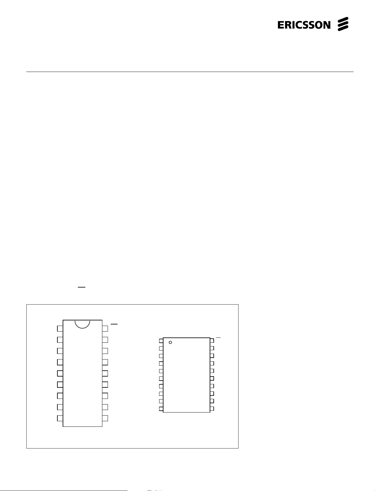
All pin numbers in this paper refer to DIP package.
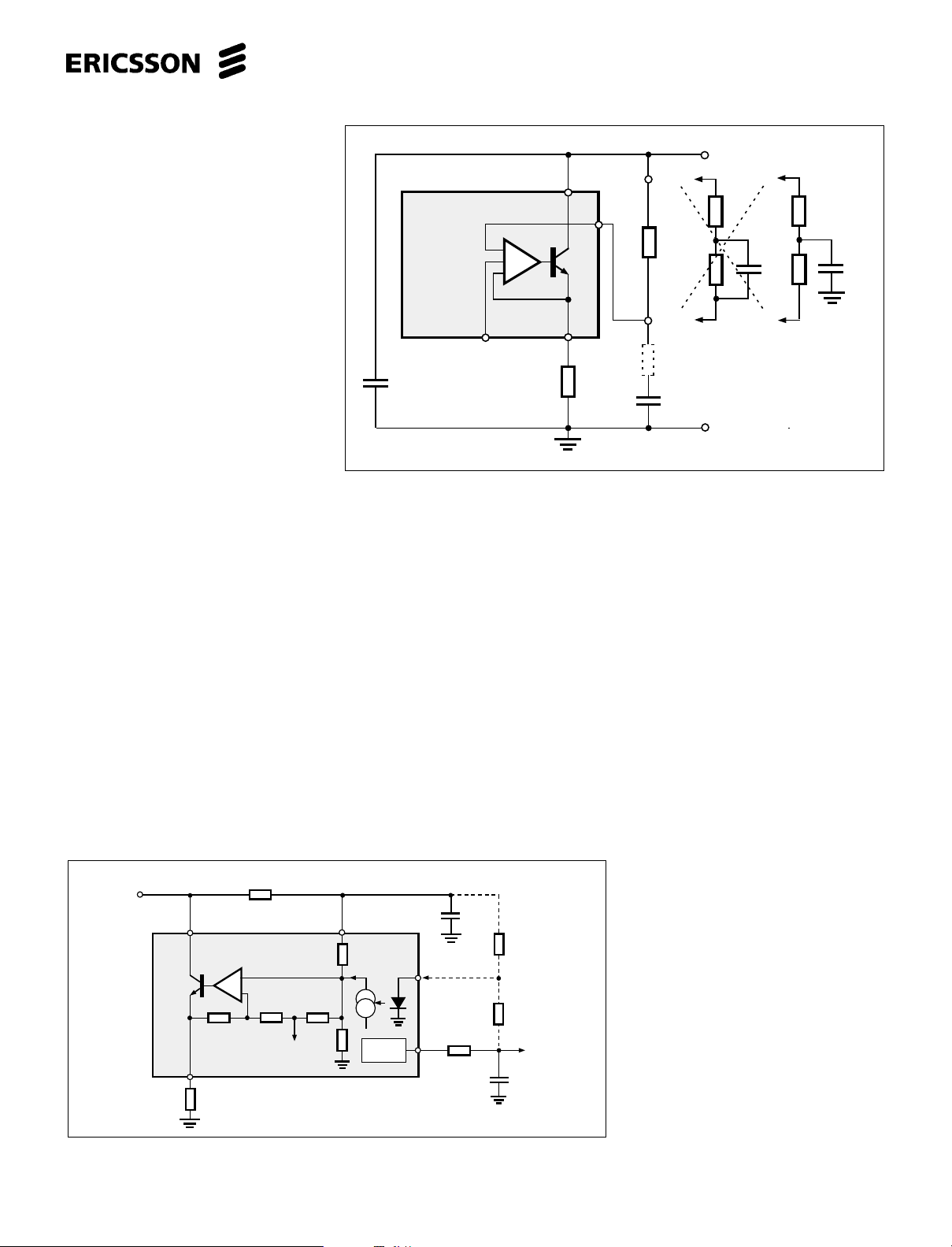
(+Line)
Power
down
6
13
+
12
DC
Ref.
supply
18 9 8
DC1 DC2
5
1
17
-
+
DC
supply
3
11
+
+
27
PBL 3852
A.
Ref.
15
10
B.
+
+
16
14
4 +
+
Telephone
line
Key Features
• Generates its own supply from the
telephone line
• Adaptive to all types of telephone line
feeding systems (i.e. 48V 2x200Ω,
60V 2x 600Ω, 48V 2x800Ω)
• Operates down to 2.1V (excl. polarity
bridge)
• Adjustable DC-characteristic to the line
• Few inexpensive external components
to function
• Easy adaptation for various market
needs
• Dialler interface with DC-supply, mute,
power -down and DTMF-input
• Confidence tone in the receiver at
DTMF-dialling
• ”Soft clipping” that prevents distortion
at high transmit signal levels
• Balanced microphone input for dynamic, and electret microphones
• Balanced receiver output for dynamic
and magnetic receiver elements
• Transmitter and receiver gain regulation for automatic loop loss compensation (disabled in mute mode)
• Four separate DC supplies for different
requirements
• High gain of the receiverfacilitates
volume control function
• Microphone cut-off function possible
by a switch
• All gain and frequency setting networks
in Rx, Tx and side tone are referred to
ground
• Excellent RFI performance
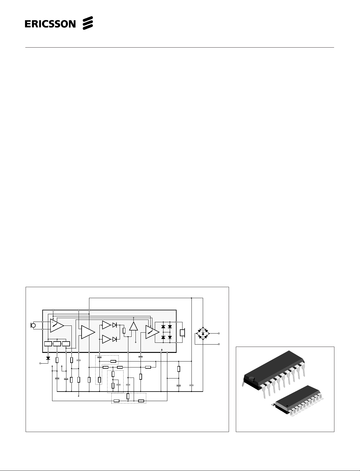
PBL3852
DTMF
A. Dynamic limiter
B. Sidetone network
C. Gain regulation with line length
Figure 1. Functional diagram.
C.
(-Line)
PBL3852
18-pin plastic DIP 20-pin plastic SO
1
Page 2
PBL 3852
Maximum Ratings
Parameter Symbol Min Max Unit
Line voltage, T
Line current, continuous DIP I
Line current, continuous SO package I
Operating temperature range T
Storage temperature range T
Input level (all inputs) 0+C V
R
feed
+
E= 48.5V
= 2 s V
p
MUTE
R = 0-4KΩ
L
0 ohm when artificial
line is used
5H+5H
= 400Ω+400Ω
C = 1µF when artificial line is used
470µF when no artificial line
+
C
V
600Ω
2
V
1
ARTIFICIAL
LINE
I
L
V
V
DC2
L
V
M
+ LINE
I
DC2
I
DC1
V
DC1
PBL 3852
with external
components
See fig. 4
MIC
REC
V
4
- LINE
L
L
L
Amb
Stg
Z
= 150Ω
Mic
V
3
Z
= 150Ω
Rec
022 V
0 130 mA
0 100 mA
-40 +75 °C
-55 +125 °C
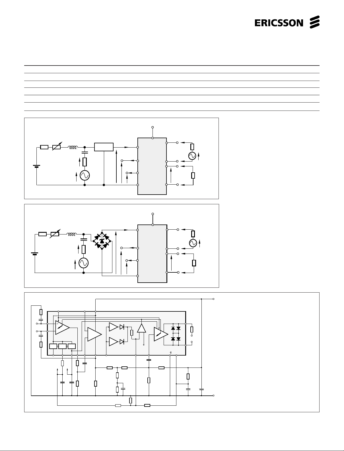
Figure 2. Test set up without rectifier
bridge.
MUTE
V
M
R
+
E = 48.5V
= 400Ω+400Ω
feed
R = 0-4KΩ
L
5H+5H
V
V
1
1µF
2
Uz= 15-16V
+
600Ω
I
L
+ LINE
PBL 3854
with external
components
See fig. 4
MIC
REC
V
4
V
L
I
DC2
V
DC2
I
DC1
V
DC1
Z
= 150Ω
Mic
V
3
Z
= 150Ω
Rec
- LINE
Figure 3. Test set up with rectifier bridge.
REC
+
R24
C10
(+Line)
(-Line)
R22
C12
MIC
C13
R23
Mute
6
13
+
12
DC
Ref.
supply
18 9 8
R3
DC1 DC2
+
C2
C3
supply
DC
R4
+
5
3
11
R5 R7
1
27
C4
PBL 3852
R9 R11
R12
R13
R14
R15
17
-
+
+
Ref.
15
10
C8
R18
R17
C6
R16
16
14
4 +
R19
+C
C9
Figure 4. Reference figure with line length regulation. (Application for dynamic microphone)
R1 = - C1 = R2 = - C2 = 47µF
R3 = 100Ω C3 = 47µF
R4 = 7.5k C4 = 68nF
R5 = 33k C5 = R6 = - C6 = 100nF
R7 = 75Ω C7 = R8 = - C8 = 47nF
R9 = 620Ω C9 = 47µF
R10 = - C10 = 15nF
R11 = 6.2k C11 = R12 = 130Ω C12 = 0.15µF
R13 = 2.4k C13 = 0.15µF
R14 = 27k
R15 = 18k
R16 = 120k
R17 = 18k
R18 = 62k
R19 = 910Ω
R20 = R21 = R22 = 10k
R23 = 10k
R24 = 150Ω
2
Page 3
Electrical Characteristics
At T
= + 25° C. No cable and no line rectifier unless otherwise specified.
Amb
PBL 3852
Parameter fig. Conditions Min Typ Max Unit
Line voltage, V
note 1 2 IL = 15 mA 3.3 3.7 4.1 V
L
Transmitting gain, note 1 20 •
Transmitting range of 2 1 kHz, R
regulation
note 1
Ref.
2I
2R
2R
2R
= 100 mA 11 13 15 V
L
10
log (V2 / V3); 1 kHz
= 0 414345dB
L
= 400Ω 43.5 45.5 47.5 dB
L
= 900Ω - 2200Ω 46 48 50 dB
L
= 0 to 900 ohm 3 5 7 dB
L
Transmitting frequency 2 200 Hz to 3.4 kHz relative to 1 kHz -1 1 dB
response
Receiving gain, note 1 20 •
2R
2R
2R
Receiving range of regulation 2 1 kHz, R
10
log (V4 / V1); 1 kHz
= 0Ω -13 -11 -9 dB
L
= 400Ω -10.5 -8.5 -6.5 dB
L
= 900Ω - 2200Ω -8 -6 -4 dB
L
= 0 to 900Ω 357dB
L
Receiving frequency response 2 200 Hz to 3.4 kHz relative to 1kHz -1 1 dB
Microphone input impedance 2 1 kHz, 1.7 kΩ
pin 12 (14),13 (15)
Transmitter input impedance 2 1 kHz 17 kΩ
pin 3
Transmitter dynamic output 2 200 Hz - 3.4 kHz 1.5 V
≤ 2% distortion, IL = 20 - 100 mA
Transmitter max. output 2 200 Hz - 3.4 kHz 3 V
IL = 0 - 100 mA, V3 = 0 - 1 V
Receiver output impedance 2 1 kHz, R
= 0Ω, note 4 32(+150) Ω
L
Receiver dynamic output 2 200 Hz - 3.4 kHz 0.5 V
≤ 2% distortion, IL = 20 - 100 mA
Receiver max. output 3 Measured with line rectifier 0.9 V
200 Hz - 3.4 kHz, IL = 0 - 100 mA
V
= 0 - 50 V
Transmitter output noise 2 Psoph-weighting, Rel 1 V
Receiver output noise 2 A-weighting, Rel 1V
1
rms
, RL = 0 -75 dB
rms
, with cable -80 dB
0 - 5 km, ø = 0.5 mm note 3
0 - 3 km, ø = 0.4 mm
Mute input current 2 20 µA
DC1-supply voltage 2 I
DC2-supply voltaget (clamp) 2 I
= (20 - 100) mA note 2 1.75 2.0 2.25 V
L
I
= 1 mA
DC1
= 20-100 mA see text, I
L
= 1.9 mA note 2 3.4 3.7 4.0 V
DC2
at zero signal in the receiver amplifier
p
p
p
p
Psoph
A
Notes
1. Adjustable to both higher and lower values with external components.
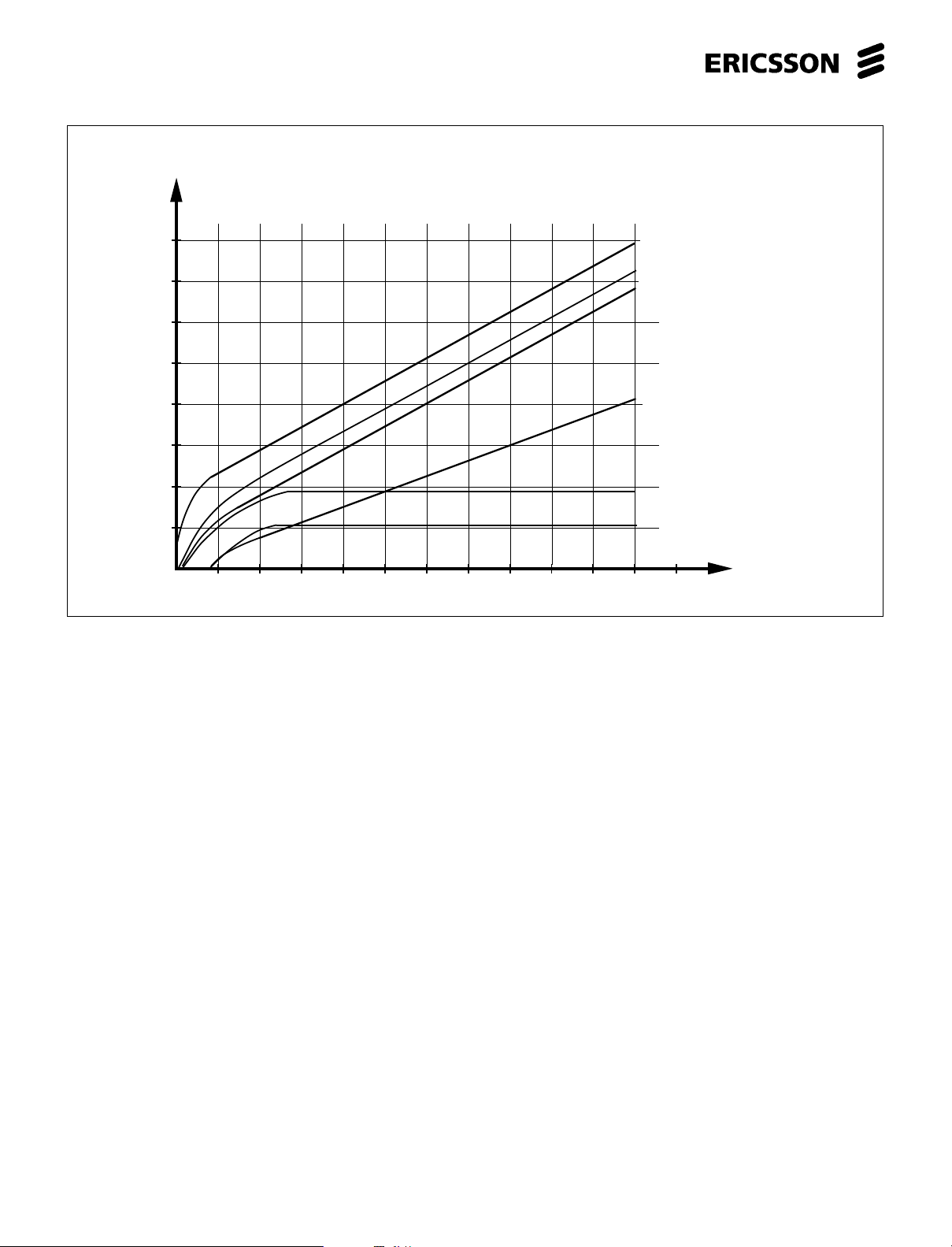
2. Lowest line current dependent of the set DC-characteristic. See page 14, fig 8.
3. Psofometric weighting will give (6-7) dB lower value. (-dB)
4. 150 ohm resistor in test set up.
3
Page 4
PBL 3852
Pin Description
DIP SO Symbol Description
1 1 +L Positive line terminal
2 2 TO Slope setting for DC characteristic and sidetone balancing signal output
3 3 TI Transmitter amplifier input
4 4 +C Internal power supply
5 5 DCC Line voltage DC level adjustment input
6 6 MUTE Transmitter and receiver amplifier mute input
7 7 RCT Dynamic limiter ”soft clipping” input
8 8 DC2 DC supply 2 output, typically 3.7 V
9 9 DC1 DC supply 1 output, typically 2.1 V
10 NC Not connected
11 NC Not connected
10 12 GR The output of the rectifier to the dynamic limiter and gain regulation input
11 13 MO Microphone amplifier output
12 14 MI1 Microphone amplifier non-inverting input
13 15 MI2 Microphone amplifier inverting input
14 16 -L Negative line terminal
15 17 RI Receiver amplifier input
16 18 RO1 Receiver amplifier inverting output
17 19 RO2 Receiver amplifier non-inverting output
18 20 PD Power down input
+L
1
TO
2
TI
3
+C
4
DCC
5
6
Mute
7
RCT
8
DC2
DC1 GR
9 10
18
17
16
15
14
13
12
11
PD
RO2
RO1
RI
-L
MI 2
MI 1
MO
TO
+C
DCC
Mute
RCT
DC2
DC1
+L
NC
1
2
3
TI
4
5
6
7
8
9
10
20
PD
19
RO2
18
RO1
17
RI
16
-L
15
MI 2
14
MI 1
13
MO
12
GR
11
NC
DIP SO
Figure 5. Pin configuration.
4
Page 5
Functional Description
Design procedure
1. Set the circuit impedance to the line,
either 600Ω or complex. (R19 and C9).
C9 should be big enough to give low
impedance compared with R19 in the
telephone speech frequency band.
Too large C9 will make the start-up
slow.
2. Set the DC-characteristic that is
required in the PTT specification or in
case of a system telephone in the PBX
specification (R7). There are also
internal circuit dependent requirements
like supply voltages etc.
3. Set the attac point where the line length
regulation is supposed to cut in
(R14,R15 and R16). Note that in some
countries the line length regulation is
not allowed. In most cases the
end result is better and more readily
achieved by using the line length
regulation (line loss compensation)
than without.
4. Set the transmitter gain, regulation and
frequency response. See text for the
dynamic limiting feature.
5. Set the receiver gain and frequency
response. See text how to limit the
max. swing to the earphone.
6. Adjust the side tone balancing network.
7. Set the RFI suppression components
in case necessary. In two piece
telephones the often ”helically” wound
cord acts as an aerial where especially
the microphone input with its high gain
and input impedance is the more
sensitive.
+Line
1
2
R7
Figure 7. System of DC-Characteristic.
R19
PBL 3852
+
-
Ref=1.16V
PBL 3852
1
4
3
C10
2
R7
Figure 6. AC-impedance.
Impedance to the line
The AC- impedance to the line is set by
C10, R19 and C9. Fig. 6. The circuits
relatively high (≈ 20k with R7 = 75Ω)
parallel impedance will influence it to
some extent. At low frequencies the
influence of the C9 can not be neglected.
Series resistance of the C9 that is
dependent on temperature and quality will
cause that some of the line signal will
enter pin 4 and generate a closed loop in
the transmitter amplifier that will create an
active impedance thus lowering the
impedance to the line. The impedance at
high frequencies is set by C10 that also
acts as a RFI suppressor.
In many specifications the impedance
towards the line is specified as a complex
network. See fig. 6. In case a) the error
+
C9
4
- I pin5
DCsupply
5
I pin5
9
R3
+
R20
R21
DC1
C2
PBL 3852
+Line
a) b) c)
R19
Rs
≈1Ω
+
signal entering pin 4 is set by the ratio
≈Rs/R19 (909Ω), where in case b) the
ratio at high frequency will be Rs/220Ω
because the 820Ω resistor is bypassed by
a capacitor. To help up this situation the
complex network capacitor is connected
directly to ground, case c) making the
ratio Rs/220Ω+820Ω and thus lessening
the error signal. Conclusion: Use case c)
when complex impedance is specified.
DC - characteristic
The DC - characteristic that a telephone
set has to fulfill is mainly given by the
network administrator.Following parameters are useful to know when the DC
behaviour of the telephone is to be set:
• The voltage of the feeding system
• The line feeding resistance 2 x.... ohms
• The maximum current from the line at
zero line length
• The min. current at which the telephone
has to work (basic function)
• The lowest and highest voltage
permissible across the telephone set.
• The highest voltage that the telephone
may have at different line currents is
normally set by the network owners
specification. The lowest voltage for the
telephone is normally set by the
different voltages that are needed for
the different parts of the telephone. For
ex. for transmitter output amplifier,
receiver output amplifier, dialler,
speech switching and loudspeaker
amplifier in a handsfree telephone etc.
Example:
The complex network
220Ω + 820Ω//115nF
C9
-Line
5
Page 6
PBL 3852
V
16
14
12
10
8
6
4
2
20 40 60 80 100 120
Figure 8. DC-Characteristics. (R7 = 75 Ω)
V
circ
. =
I
PIN
4
⋅
R
19
+k1⋅
Vref+R
a
=
I
pin
5
⋅5.5⋅10
3
if function DC−control at pin5is used
()
7
⋅
V telephone line
V line
V pin 4
V pin 2
V pin 8
V pin 9
I
L
mA
I
line
+
k
2
⋅
V
pin
2
+
a
k
1
⋅
V
ref
= 1.1
V
k
2
⋅
V
pin
2
= 0.5⋅
I
PIN
4 ≈
1
mA
The R7 will set the slope of the DC-char.
and the rest of the level is set by some
constants in the circuits as shown in the
equation. The slope of the DC-char. will
also influence the line length regulation
(when used) and thus the gain of both
transmitter and receiver. R7 acts also as
current protection for the circuit, must be
considered when low values are to be
used. The level of DC-characteristic can
be adjusted up at input pin 5 (some
100mV´s). The R21 adjusts a fix amount
where R20 couples the adjusted value to
line current. See fig. 32.
Microphone amplifier
The microphone amplifier in the PBL
3852 is divided into two stages. The first
stage is a true differential amplifier
providing high CMRR (-55 to -65 dB
R
7
⋅
I
line
typical) with voltage gain of 19 dB. This
stage is followed by a gain regulated
amplifier with a regulation range from 6.5
dB to 14.5 dB, see fig. 15. The input of
the microphone amplifier can be used for
electret, magnetic or dynamic transducers
see fig. 9. The PBL 3852 has basically a
higher gain regulation range (8 dB) than
the more or less standard 6 dB´s for gain
regulation with line length, this in order to
be able to be used in applications where
”softclipping” is required. In case lower
regulation range is necessary, it is
possible with some additional
components.
See reference figs. 4, 10c, 10f, 32 and
33. For an electret microphone the
circuitry will be simple, see fig. 10f. A
resistor is added from the microphone
amplifier output, pin 11, to the positive
termination of the microphone and further
via a capacitor to the - input at pin 13.
The DC supply resistors for the
microphone should be round 200Ω (in
order not to overdrive the microphone
amplifier) and the feedback resistor (17k)
is of that magnitude that it either
influences the CMRR balance at the
input or destroys the send mute by
bypassing signal round the microphone
amplifier in mute state. For a dynamic
microphone some more components are
necessary, see fig. 10c. In order not to
influence the send mute the feedback
signal is taken from transmitter output at
pin 2 and because this signal is in
opposite phase with the signal at pin 11,
it is taken to the other input at pin 12. Also
in order not to influence the DC-balance
of the microphone amplifier a capacitor
has to be included in the feedback path
and to maintain the CMRR of the
6
Page 7
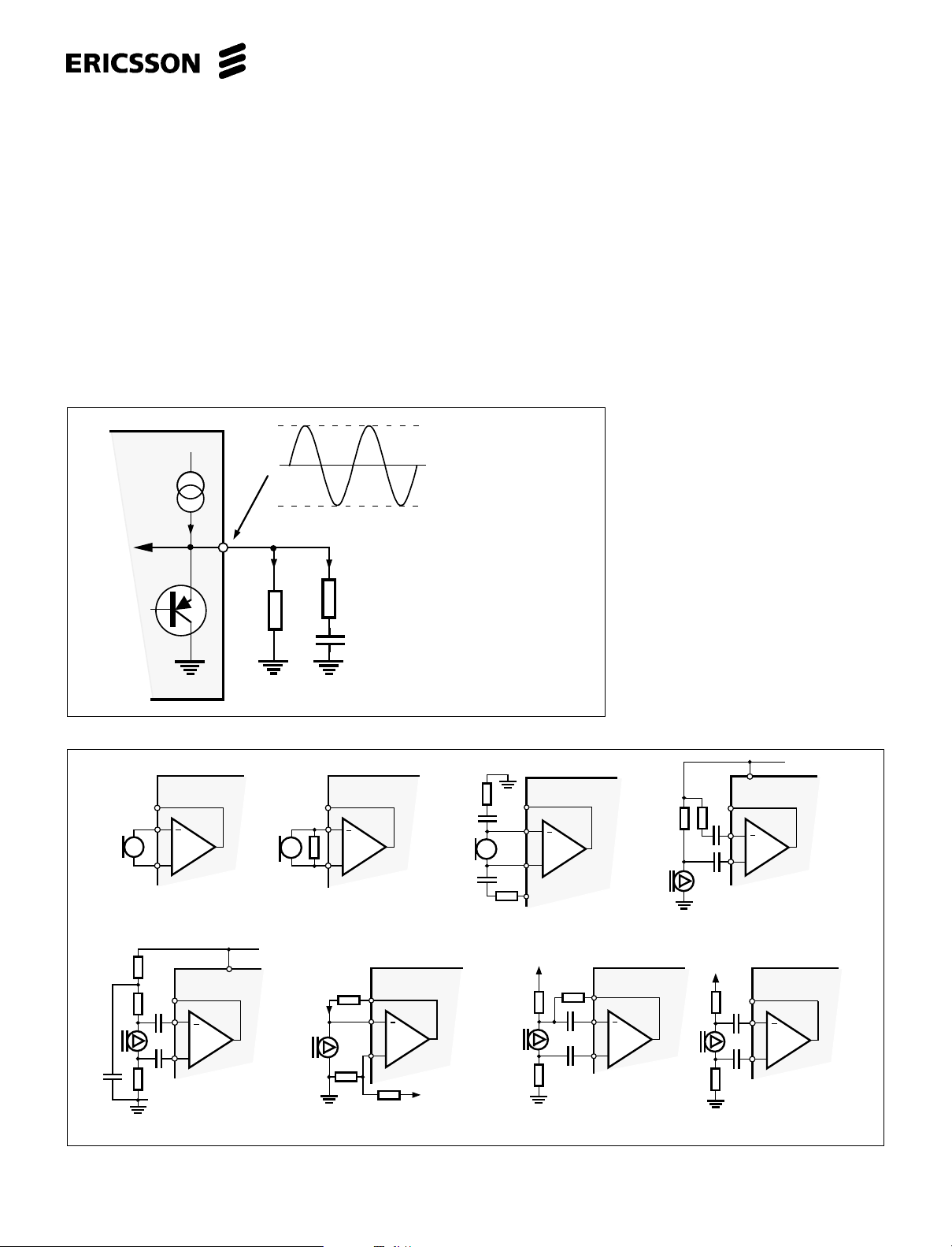
PBL 3852
microphone amplifier a similar RC
combination ought to be connected from
the other input, pin 13, to ground.
An electret microphone with a built in
FET amplifier is to be seen from outside
as a high impedance constant current
generator and is normally specified with a
load resistance of ≈ 2k. This is to be
considered as max. value and by using it
will render the max. gain from the microphone. This level of input signal that is
unnecessary high will result in clipping in
the microphone amplifier and in mute
condition permeate through the input to
Strong
cc gen.
11
DCload
ACload
the circuits reference and this way to all
functions, resulting among other things in
a bad mute. Hence it is better regarding
noise perfomance and mute to rather use
the gain of the microphone amplifier than
the gain of the microphone itself (in case
of electret) flat out. A more suitable level
of gain from the microphone is achieved
by using a load resistance of 200 - 470Ω.
Gain setting to the line is done at the
input of the transmitter.
It is possible to use the microphone
amplifier as a limiter ( added to the limiter
in the transmitter output stage ) of the
DC ( ref. ≈ 1.16V )
ref. minus a diode ≈ 0.5V
DC-load = R4+R5
DTMF
) //Z
AC-load = R4+R5// (R6+Z
Z
DTMF
= DTMF generator impedance
TI
transmitted signal (See fig. 9). The
positive output swing is then limited by the
peak output current of the microphone
amplifier. The negative swing is limited by
the saturation voltage of the output
amplifier. The output of the amplifier is
DC-vice at internal reference level
(1.16V). The lowest negative level for the
signal is reference minus one diode and
sat. transistor drop (1.16-0.6-0.1 = 0.46V).
The correct clipping level is found by
determining the composite AC- and DCload that gives a maximum symmetrical
unclipped signal at the output. This signal
is then fed into the transmitter amplifier at
a level that renders a symmetrical signal
clipping on the line. (adjust with ratio R4,
R5) The total transmitter gain when an
electret microphone is used can then be
adjusted with the load resistor of the
electret microphones buffer amplifier.
Figure 9. Microphone amplifier output clipping.
(a)
R
C
+
PBL 3852
11
13
M
12
+
Dynamic
microphone
M
+
4
PBL 3852
(h)
11
13
12
Balanced electret microphone.
An additional RC filterlink is
recommended if pin 4 is used
as a supply.
(b)
11
13
12
+
Magnetic
microphone
(g)
Im
Rx
Mic. ampl. supplies the mic.
current Im, set by Rx and Ry.
Figure 10. Microphone solutions.
PBL 3852
M
11
13
12
PBL 3852
M
+
Unbalanced electret
microphone
Ry
DC1
(c)
PBL 3852
11
13
M
12
+
For dynamic mic.with
2
reduced gain
regulation
DC1
(f)
Balanced electret
microphone with reduced
gain regulation
PBL 3852
(d)
4
11
13
M
12
+
Unbalanced electret
mic. with balanced
signal, DC-supply from
pin 4.
DC1
PBL 3852
11
13
M
12
+
(e)
PBL 3852
11
13
M
12
+
Balanced electret
microphone
7
Page 8
PBL 3852
(a),(c), (d)
(b),(e)
(f)
big C
A
small C
A
Transmitter amplifier
The transmitter amplifier in PBL 3852
consists of three stages. The first stage is
an amplitude limiter for the input signal at
TI, in order to prevent the transmitted
signal to exceed a certain set level and
cause distortion. The second stage
amplifies further the signal from the first
and adds it to a DC level from an internal
DC-regulation loop in order to give the
required DC characteristic to the
telephone set. The output for this stage is
TO. The third stage is a current generator
that presents a high impedance towards
the line and has its gain from TO to +L.
The gain of this amplifier is ZL/R7 where
ZL is the impedance across the telephone line. Hence, the absolute maxi-
11 3
R
A
(a)
C
A
11
(b)
R
A
C
mum signal amplitude that can be
transmitted to the line undistorted is
dependent of R7.(amplitude limiting) The
figure 20 shows the range for the
amplitude limiter dependent of the
operating point on the DC characteristic.
The transmitter gain and frequency
response are set by the RC-network
between the pins MO and TI (See fig. 11).
The capacitor for cutting the high
frequency end is best to be placed directly
at the microphone where it will also act as
a RFI suppressor. The input signal source
impedance to the transmitter amplifier
input TI should be reasonably low in order
to keep the gain spread down, saying that
R4//R5//R6 (see fig. 32) must be at least a
factor of 5 lower than the ZTin. Observe
that the capacitor C9 should have a
3
A
11
3
(c)
R
A
C
A
reasonably good temperature behaviour
in order to keep the impedance rather
constant. The V+C´s influence on the
transmitter DC-characteristic is shown in
the fig. 8 therefore the transmitter gain
would change if the transmitted signal
gives reason to an ac-voltage leak signal
across C9, this being a feedback point. If
the transmitter has an unacceptable low
sving to the line at low line currents
<≈10mA the first should be to examine if
the circuits DC- characteristic can be
adjusted upwards and first secondly make
use of the linear PD.
no attn.
11
(d)
C
C
R
A
C
A
R
B
attn.without dc.
C
no attn.
3
11
B
3
(e)
R
A
C
A
R
C
B
B
attenuation
R
B
attenuation
11
(f)
C
C
R
A
C
A
R
C
B
B
attn.without dc.
3
Figure 11. Different possible types of networks between microphone amplifier and transmitter.
Receiver amplifier
The receiver amplifier consists of three
stages, the first stage being an input
buffer that renders the input a high
impedance. The second stage is a gain
(a)
+
17
-
Rx
+
16
(b)
≈150Ω
150Ω
regulated differential amplifier and the
third stage a balanced power amplifier.
The power amplifier has a differential
output that does not need a series
capacitor with the load. The receiver
(c)
17
-
+
Rx
+
16
(d)
17
-
+
+
Rx
+
16
Z
amplifier uses at max. swing (4-6) mA
peak. This current is drawn from DC2
that can supply 2 mA continuous
current, the C3 helping to supply the
peaks, this applies for speech signals
only. Continuous sinusoidal signals at
this level will load the DC2 down. If a
distortion appears in the earphone
amplifier output at high signal levels,
high line currents, low ohmic earphone
load or at low frequencies, the most
probable fault is that the filtering
capacitor of the earphone amplifier
supply C3 is too small. At low line
Figure 12. Receiver arrangements.
8
currents (normal case, IL < 10 mA)
Page 9

PBL 3852
when the current and the voltage are not
enough for full signal swing in the
receiver amplifier, a sort of ”soft clipping”
is activated and lowers the gain so that
no distortion will appear. A capacitor is
needed at the output with low ohmic DC
loads (some of the earphones have
extremely low DC resistance) because
even a small DC offset at the output will
cause a great current drain from DC2
continuously. This capacitor is also
needed if DC2 is used as a back up
supply for some memories and the
isolation is not done with a diode. The
gain and frequency response is set at
the input RI with a RC-network. The
receiver gain can be regulated. The
range of regulation from the input to the
output is 5.8 dB (23.7 to 29.5dB). As
Line length regulation
Line length regulation is used to
compensate the gain loss in both transmitter and receiver due to increasing
attenuation at increasing line length.
Setting the parameters for line
length regulation (See fig.13)
The dotted line from dB axis to km axis
indicates the attenuation versus line
length that originates from the impedance
in the increasing length of the specific
cable used.It is generally desired that
there is a gain regulation that
compensates for this attenuation. The
regulation should operate across a line
length that comprises most of the
subscribers. This will give the value for
the line length P and is in most cases
given by the network owner in their
specification about the telephones
acoustical behaviour. The amount of
regulation is given by the portion of
attenuation q. The slope of attenuation
change within this area is given by q/P
mentioned before the output amplitude
can be limited by a resistor in series with
the pin 8. An other method is to connect a
series resistor with the earphone itself. In
case of no signal at the input of the
receiver, very little current is drawn from
DC2. The same is valid at mute
condition, understood that no DC current
is drawn to somewhere else, as for
example to a low ohmic DC load at
earphone amplifier output. The receiver,
contrary to most of our previous speech
circuit families, can be loaded single
ended resulting an undistorted signal. The
load should be 10x the standard (150Ω)
load of the amplifier with a capacitor in
series, without a capacitor somewhat
higher, depending on the required signal
swing. The receiver has, as a principal
(dB/km). The approximate centre point of
the gain regulated line length portion is
P/2. The line length above point P is not
regulated in any sense and therefore
followes the attenuation due to the
increase in impedance at increasing line
length.
To set the gain regulation:
1). Determine from the acoustics spec.
diagram, that is given by the network
owner, where the line length P is and
what q value has to be used (a value dB/
km = q/P) and adjust the microphone
amplifier gain regulation accordingly with
a feed back resistor between pins 11 and
13. The q value is a gain, the microphone amplifier regulation has to be set
to.The receiver gain is fixed. (normally the
transmitter and receiver regulation gains
are set to the same value, it is only in the
case of ”soft clipping” the transmitter
regulation is bigger)
2). The values of R14, 15 and 16 are
dependent of telephone station feeding
system (2 x AΩ , bat. V), line type (cable
protection, two series diodes anti parallel
across its output to limit the signal to the
earphone and thus preventing an
acoustical shock. A resistor in series with
the output can very well be used to
increase the protection level. Note, that
the noise in the receiver is allways
transmitter noise that has been more or
less well balanced out in the side tone
network.
Figure 12 b) shows a 150Ω resistor in
series with a 150Ω earphone load. This is
to minimize distortion and to decrease the
DC-load rather than using a capacitor but
it will give less swing with low line
currents, IL< 15mA.
Ω/km) and DC - characteristic of the
telephone set (see fig. 14). Therefore
calculate or measure the voltage at pin
+C at 0 and P km. (the DC - characteristic
ought to have been set at this stage) The
voltage drop a) in the graph is across the
discrete components like the polarity
guard bridge, protection components and
series transistor for LD - dialling. The
voltage drop b) is across R19 or in case
of comlex line impedance the drop across
the network. (I
current taken from pin +C ) x R19.
Condition: The network with R14, 15, and
16 should not be too low ohmic because
it would load the +C unnecessary,
increasing the DC mask. (<100µA) The
network should not be too high ohmic
either thus influencing the precision of
the current into the GR input. (≈20µA)
The GR input current<1µA.
3). Set the gains for transmitter and
receiver.
+ eventual additional
pin+C
DC1
V
GR =
1
R
14
+C
+
R
14
+
16
R
1
1
+
15
R
16
R
at 0 km : 1.237 =
To calculate R14 and R16 for ex. choose R15 = 18k.
≈ 2
R
14
1
+
R
14
0km
+C
+
R
16
1
+
R
R
15
at Pkm :1.085 =
1
16
≈ 2
R
14
1
+
R
14
Pkm
+C
+
R
16
1
1
+
R
R
15
16
9
Page 10

PBL 3852
This axis is the total gain, microphone-telephone-line-telephone station.
dB
This axis is the regulating gain of the speech circuit.
dB
b
dB
c
The point where the
regulation cuts in
can be varied.
The slope is = q/P
a
The slope of regulation can be
altered in order to compensate
the gain from 0 - P
q
a=under comp.
Amount of regulation
b=opt.comp.
c=ower comp.
approx. center
of the regulation
P/2
Regulation area
0
Figure 13. Line length regulation.
In case no regulation is desired the gain
can be locked either into low or high gain
mode. For high gain mode remove
resistors R14 and R16. For low gain
mode remove resistors R14 and R15.
The gain is set on
non regulated value
of the line
Line attenuation
Area of operation,
given by the network
specification
P
It is possible to combine dynamic
limiting and line length regulation in the
same design as shown in fig. 32. In case
no regulation but high gain is required ,
the pin GR is connected to ground via a
Line
km
resistor and if low gain is required it is
connected via a resistor to a level that
is higher than the internal reference of
1.16V. In both cases the current
through the resistor should be ≈ 20 µA
in order to ensure a good precision.
V
B (V)
Battery voltage of the system
A=1/2 battery feeding resistance
C=cable Ω/km
Is set by 2 A + C P
a
b
There must be DC "room" here at the longest specified line
for the supply of the circuit and auxiliary functions.
Figure 14. The DC-characteristic of a telephone.
10
Is set by 2 A
The slope gives regulation
precision
0P
V Line
V across circ.
V+C
(Current)
(Line resist.)
Line length km
Page 11

PBL 3852
(dB)
∆ Transmitter gain
0
-1
-2
-3
-4
-5
-6
Full regulation
-7
-8
1.00 1.05 1.10 1.15
at P km
Same amount of
regulation as in the
receiver
1.20
1.25
at 0 km
DC pin GR
(V)
Figure 15. Transmitter line length regulation. How to determine the voltage at pin GR for a certain line length 0-P at a certain
regulation of gain.
(dB)
∆ Receiver gain
0
-1
-2
-3
-4
-5
-6
DC pin GR
1.00 1.05 1.10 1.15
Figure 16. Receiver line length regulation.
1.20
1.25
(V)
11
Page 12

PBL 3852
Dynamic limiter
The dynamic limiter consists of a full wave rectifier that senses the signal amplitude on the line and produces a control signal that
reduces the gain of the transmitter and the receiver when the signal on the line reaches a certain set level. The reason to this is to
reduce distortion at high signal levels (See fig. 15, 16, 17, 18 and 34).
The attac point for the dynamic limiter is set by the voltage divider R8, R10 and the internal resistor of 30k (peak signal) the lower
frequency limit is set by the input capacitor C5 to pin 7 (RTC). The diodes Da and Db that make the function logarihtmic have a 0.6V
voltage drop on this signal which is then added to the reference ≈0.855V. The signal will be further rectified with a ratio 1:1, attenuated
(can be neglected) in the filter at pin GR and forvarded to the gain regulation.
At a enough high signal in, the voltage at pin GR is set by:
R
8
//30
V
pinGR
≈
V
2
peak
⋅
R
10
+
The time constant ”up” is set by the internal ≈ 2.2k and C7, where the time constant ”down” is R14 parallel with R15 and C7. The
DC-voltage at pin GR with no input signal is set by the resistor divider R14 and R15 at a level just below where regulation starts see
fig. 16. It is possible by adjusting this DC-level down to make the time constant ”up” longer. With no AC signal in, or a very small and
no resistors R14,R15 the rectifier output is at reference in level (0.855V). At no AC signal in the voltage at pin GR is set up by:
R
V
pinGR
=
V
DC
1⋅
R
15
14
+
R
15
R
8
//30
k
− 0.6 + 0.855
k
If gain regulation with line length is used together with softclipping the time constant ”down” will be influenced by the parallel value of
R14,R15, and R16. The DC-level at pin GR without AC signal will be set by these three resistors.
V
2
Vp
2.25
2
1.75
1.5
1.25
1
0.75
0.5
0.25
Figure 17. Dynamic limiter.
12
12
Vin +10dB +15dB +20dB
3
45
6789
10 11
12
13
14
mVp
V
3
Page 13

PBL 3852
Figure 18. The dynamic limiter function
16
14
Line
R10
R8
V
C5
RTC
Da
7
Db
Int. ref.0.855V
30k
Rectifier output
In ref.=0.855V
Signal at GR without C7
To gain regulation
Ref.
(1.16V)
2.2k
0V
10
C7
GR
R14
+
R15
Amplitude limiter
V
L
DC 1
Figure 19. Transmitter output signal
.
See fig. 22 for data.
limiter
Power down and input PD
During pulse dialling or register recall
(time controlled line break) the telephone
line is interrupted, hence the transmission and peripheral circuits are not
supplied during the breaks from the
line.The circuit has therefore an internal
power-down function that automatically
shuts down the current consuming parts
when the line voltage drops under a
certain level. This function reduces the
internal current consumption I+C
to≈120µA that in its turn minimizes the
charge up time of the capacitor C9 when
the line feed returns. The timing and pulse
shape at LD - dialling is improved. In
some cases the parameters around LD -
12
10
8
6
4
2
20 40 60 80 100 120
dialling can be improved by switching the
voltage at this input. Most of the modern
processors used for LD-dialling do also
supply a ”window” signal for the duration
of the LD-digit stream. This signal can be
used for the PD input. An improvement of
receiver and transmitter output swing at
very low line currents (IL<10mA) can be
achieved by controlling this PD input with
two resistors and a diode, maybe a
capacitor C1 is necessary, see fig. 21.
The circuit can be made to work down at
1.8V line voltage and 2.8mA line current.
Great care has to be taken to secure
against a possible latchup.
The PD input should not be held ”down”
at hook-on or at start to hook-off this
Amplitude limiter
IR+
S
7
V
(1x diode
V
Tsat
1x Vce)
Tline4Vp-p
I
L
mA
restricting the internal reference voltage
buid up and the circuit to ”wake up”. (It is
good practice to isolate the input with a
diode according to fig. 21, an open
collector drain can also be used). If the
adjusting feature with the two resistors is
used, it does not endanger the ”waking
up” process because the line voltage via
R19 will lift the level at PD input over the
critical reference voltage level of 1.16V. In
case this input is not used it should be left
”open”.
13
Page 14

PBL 3852
+
Figure 20. Power down input.
Figure 21. Mute input.
PBL
3852
2
14
39Ω
Digital control
PBL
3852
I
Mute
6
Mute
14
V
Mute
PBL
PD
18
I
or
PD
-LTO
in
I
Mute
MO
V
Mute
-L
in
PBL
3852
11
14
-L
Microphone mute only
14
-L
3852
> Ref. (1.16V)+diode
Linear control. Is effective only at line
currents <10mA. (also dependent of
DC-characteristic)
PBL
3852
11
MO
100
C
Ω
18
PD
PBL
3852
Rx
15
Muting
C8
points
Receiver mute only.
C1
R1
>Ref.
R2
17
16
Mute function
The circuit has a mute function at pin 6.
By sourcing current into this pin will cut off
the gain in the microphone amplifier
(attenuation min. 60dB) and decrease the
gain in the receiver amplifier to reach the
confidence tone level at DTMF-dialling.
The receiver mute is ≈-40dB down from
the unmuted value to satisfy those who
keep the handset close to the ear at
dialling. For users who keep the handset
from the ear the confidence tone level is
too low. To alter the level, a signal can be
taken from DTMF generator output to
receiver input before the capacitor C8.
The added impedance to this point will
hardly disturbe the signal condition in
active speech mode. The microphone
amplifier only, can be muted by draining
current from the output pin MO. See fig.
21. In case it is required to mute the
receiver only, it can be done by shorting
the receiver input to ground before or
after the input capacitor. Shorting the
input pin to ground (does not have to be
absolute ground) actuates a mute by
driving the amplifier into saturation thus
blocking the signal path and rendering a
mute with high attenuation but will cause
a DC-level shift at output which in its turn
will cause a ”click ” in the earphone. This
can be softened with a slower mute signal
flank. If the second approach, grounding
before the input capacitor is chosen, the
grounding has to be low ohmic in order to
render a high attenuating mute.
DTMF (Dual tone multi frequency) input
The DTMF signal is added between the
microphone and transmitter amplifiers, an
input that can be seen as a summing
point for signals to be transmitted to the
line. See fig. 32. Dialling connected like
this will render a confidence tone in the
receiver at mute condition.
Start up circuit
The circuit contains a start up device
which function is to fast charge the
capacitor C9 when the circuit goes into
hook- off condition. The fast charge circuit
is a thyristor function between pins 1 and
4 that will stop conducting when the
current drain at pin 4 is lower than ≈ 700
µA + the internal current consumption.
( about 1 mA) This circuit can not
retrigger before the voltage level at C9
DC-control DCC input
The circuit has a DC- control input that
can adjust the DC-characteristic. When
a current is sourced into this pin the line
voltage will increase for a given line
current. This will enable an increased
negative swing for both the transmitter
and receiver at low line currents. If this
function is used together with LD - dialling
care must be taken that the DC-level of
the pulses is according to the
specification. The two adjustment paths
shown in the fig. 33 will have following
functions: Using R20 will alter the
adjustment with changing line current
where by using the path with R21 renders
a fix adjustment. If the input is not used it
can be left open or grounded to pin 14.
Power supplies DC1, DC2,
V+C and VPh (see fig. 22)
The PBL 3852 generates its own DC
supply V+C dependent of line current with
an internal shunt regulator. This regulator
senses the line voltage VL via R19 and
line current via R7 in order to set the
correct V
the required DC characteristic for a given
so the circuit can generate
+C
14
Page 15

PBL 3852
line resistance R
data of the exchange. A decoupling
capacitor is needed between pins +C and
-L. The V+C supply changes its voltage
linearly with the line current. It can be
used to feed an electret microphone.
Caution must be taken though not to drain
too much current out of this output
because it will affect the internal quick
start circuit by locking itself into active
state. (max. permissible current drain
600µA)
Care has to be taken when desiding the
resistance value of R19. All resistances
that are applied from +Line to ground
(-Line) will be in parallel, forming the real
impedance towards the line. This will
sometimes result in, that the ohmic value
of R19 is increased in order to comply to
the impedance specification towards the
line. The speech circuit sinks ≈ 1mA into
the pin 4, which means that the working
voltage for the speech function +V will
decrease with the increasing R19, thus
starving in the end the circuit of its
working voltage. This dependency is often
falsely taken as a sign of that the circuit
does not work down to the low line current
specified, but in fact it is the working
voltage at pin 4 that has became too low.
It is obvious that this problem is also
connected into what kind of DC-
and the line feeding
Line
characteristic is set (see fig. 22). in series with the output to isolate a DC
The circuit has further two temperature
and line current compensated DC
supplies DC1 and DC2. DC1 is a high
precision voltage supply for supplying
microphones, opto couplers etc. it is also
suitable as a voltage reference. Typical
voltage 2.1V down to line voltage of 4.1V,
in case the line voltage is lower than 4.1V
calculate; actual line voltage minus 1.9V.
In order to prevent noise entering the
line, a resistor is recommended in series
with this output.
DC2 is a voltage clamped current
source that is suitable to be used in
supplying diallers and micro processors
but also parts of circuitry that need supply
in hook on condition. The typical voltage
is 3.7V down to line voltage of 4.75V If the
line voltage is lower than 4.75V calculate;
actual line voltage minus 1.25V. The
current supply to a memory retention
capacitor is easiest isolated with a diode,
the capacitor preferably a low voltage
drop type, and in hook on condition it has
to have charge path from an uninterrupted
point on the + line. If a diode is not used
for isolation care must be taken that no
current can be taken out of the reservoir
capacitor at or after ”hook-on”. It must be
secured that the receiver can not get any
input signal and that there is a capacitor
load. It is possible to feed an external
shunt regulator directly from the DC2
output for lower voltage than the clamp
level. The line voltage can for a short
period of time go below the voltage at
this output without affecting the line
characteristics, this because the circuit
tries to keep the current taken from the
line constant at all times. The receiver
has its current supply (pt. a in fig. 22)
from the DC2 supply. A series resistor at
the output will limit the peak current
which is one way to limit the possibility
for an acoustic shock at the earphone.
The handsfree circuits ( PBL 3786,
3786/2 and 3880) speech switching
function can be supplied directly from this
output.
The fourth DC-supply VPh has an
advantage that it does not influence the
circuits DC characteristics even at high
current drain. The supply has a floating
ground reference and is used to supply
the power amplifier of a handsfree
telephone. (PBL 3786, 3786/2 and 3880)
These circuits have a current controlled
charging of the supply capacitor and the
control signal is taken across the
resistorR7.
In case a monitor amplifier is required
where the ground reference is hardly
necessary, it can be supplied from VPh .
I
L
V
L
R
L
V
+C
R
feed
+
V
E
Figure 22. DC-supplies.
+Line
DCC
R
19
+
C
+
4
a
DC2
+
C
9
PBL 3852
I
ClampClamp
+
8
+
C
3
+
-
DC1
Ref
V
+
Lim
9
DC1DC2
TI
R
3
+
C
2
5
I/U
+
-
14
3
+L
1
I
T
V
T
R
Ph
I
Ph
T
V
+
Ph
C
Ph
-Line
ƒ
2
-L
TO
I
S
R
7
15
Page 16

PBL 3852
R
18
〉〉
Z
line
//
R
19
R
9
〉〉
R
7
Z
bal
=
R
12
,
R13and C
6
PBL 3852
Rx
8
DC2
+
C3
Figure 23. DC-2 supply of peripheral circuits and memory retention.
14
-L
HANDSFREE
PBL 3786
PBL 3786/2
PBL 3880
PBL 3881
V+
+
DIALLER
V+
MEMORY
GND
Uninterrupted
+
Line
D2
(Shottky)
V+
+
Large electrolytic
or "Gold cap".
Current
thief
GNDGND
Side tone suppression (see fig. 24, 26)
The side tone suppression is achieved by adding two signals V+L and VTO in opposite phase at input RI. Because of the complex
line impedance Zline, VTO must be compensated by Zbal in order to get the correct level and phase for the signal to be summed.
Maximum compensation is achieved when following conditions are fulfilled:
drops below 2V or the line voltage below
R
7
R
This gives Z
R
to be:
bal
11
=
9
R
Z
line
//
18
R
Z
bal
=
19
R7R
R9R
1
R
1
+
9
R
18
11
Z
line
11
1
//
1
+
Z
bal
1
R
1
−
19
R
1
−
9
R
11
C10 is omitted in the equation
Following should be noted at designing the side tone network:
The impedance of the side tone network in parallel with the R7 should not be too low. This does influence the transmitter gain
and frequency response. (Z
R11 should not be low compared with Zbal this will influence the receiver frequency response. (R11 >> Zbal)
The side tone network impedance, parallel with the receiver input impedance Zin, should not be too high compared with Zin this
influencing the spread in the receiver gain. ( Zin >> side tone network impedance, R18//R17// (R11+R9//Zbal ))
Maximum compensation without any assumption is obtained when following condition is fulfilled:
R
7
R
7
+
R
In practice Zline varies with the line type, length and the feeding system parameters. Therefore Zbal should be chosen to give a
satisfactory side tone suppression at an average line length.
An other method is to make R18 complex. See fig.25. This will be advantageous in case the R7 is low ohmic (10-39Ω) because
this coupling will give +6 dB more signal for the side tone balancing. Warning! At low values of R7 the circuit will have an insufficient overcurrent protection. A over voltage protection with lower limiting level has to be used across the circuit. It also will make
it possible to implement a better working volume control for the earphone. There will be some disadvantages as: More difficult to
trim and it needs closer tolerance components.
16
9
=
R
+ Rg >> R7)
bal
Z
11
Z
line
line
//
//
R
R
19
19
+
R
1
18
R
1
+
R
+
11
Z
9
1
bal
R
7
/
R
9
−
R
7
+
R
9
Page 17

I
L
V
+L
R
18
R
R
V
TO
Z
R
7
119
R
bal
Z
17
bal
= R12, R13 and C
RI
Figure 24. Sidetone balance.
PBL 3852
PBL 3852
2
R7
R11
R17
R
Z
19
line
Z
in
6
Figure 25. Side tone network with complex R18.
C8
15
*
C
R18
Z
bal.
* To give receiver flat
frequency response
+Line
What is balancing the side
tone ?
To understand that balancing the side
tone is needed to lower the amplitude
that reaches ones own ear of the signal
that is transmitted from ones own
microphone to the line and that enters
the receiver quite normally from the line.
That in presence of a strong side tone
signal one is disturbed by it and
instinctively lowers ones voice level, but
again if the balance is too good (seldom
the case) the earphone will feel ”dead”.
In practical terms, what is expected, is
the same amplitude of ones own voice in
the ear as without the hand- set. The
need to lower the side tone level where
no balancing has been done is in the
order of one power of ten (20 dB).
To understand the principle both
theoretically and practically. See text.
Be sure to understand the balance that
is influenced by outer factors like, the
impedance of the line and the signal that
enters the ear acoustically directly from
the mouth through the handset. The
signal that enters the microphone from
the earphone acoustically will also
influence the return loss.
To understand the signal treatment
that is at hand. In other words that the
side tone network can be trimmed to
form a veritable ”distortion analyser”, so
that all the distortion that is present from
the microphone even if it is small, will be
the only signal entering the earphone.
This will sound very bad. It is better to
induce some of the fundamental
frequency back by making the balance
less perfect at that frequency. This is
valid for a network that is trimmed to only
one frequency. It is to strive to trim the
network such that it will at all line
combinations attenuate the harmonics
the same as the fundamental frequency.
To understand that if one of the two
signals entering the balancing system
from either direction, direct from
microphone or via the line, is clipped will
result in a very distorted signal entering
the receiver amplifier and thus the
earphone. Further, to remember that side
tone is a small signal that is the difference
of two large signals and that the distortion
The AC-signal at point c is now 1/10 of
the signal on the line because it was
further divided by two from point b.
(R9≈Zbal).
Hence 10 x R11 ≈R18 to satisfy the
balancing criteria.
R17 is to set the receiver gain. (can be a
volume control potentiometer)
can be up to ten times the fundamental
frequency.
Note #1 These values ensure that the
frequency behaviour of the transmitter is
A short guidance for understanding the side tone
principle (see fig. 26)
Assume the line impedance to be 600Ω.
Z1 = Line impedance
Z2 = The telephone set impedance 600Ω
Z1//Z2 = 300Ω
R7 will have a certain value 39 - 100Ω to
give the telephone a specified DC-
not influenced. With the ratio 1/10 the
influence is 1 dB, and with t ratio 1/20 it´s
0.5 dB.
Note #2 If the R9 is made low ohmic
compared with Zbal, it will load the latter
and result in a bad side tone perfomance,
again if the R9 is made high ohmic
compared with Zbal a low signal to
balance the side tone will result and make
the balancing difficult.
characteristic.
Assuming this DC-characteristic will
require R7 = 60Ω Hence it will be 1/5 of
the Z1//Z2.
This will also give 1/5 of the AC-signal
that is on the line across R7.
Note that the signals at points a and b are
180 degrees off phase.
10 x R7 ≈ R9 + Zbal note #1
R9 ≈ Zbal note #2
a
1
PBL 3852
Tx Rx
b
R7
2
R9 R11
R12
15
c
Zbal
R13C6
Making any of the impedances
unnecessary high will make the circuit
sensitive to RFI. All values given here are
approximate and serve as starting entities
only. The final trimming of side tone
network is a cut and try proposition
because a part of the balance lies in the
accoustical path between the microphone
and earphone.
17
16
R18
R17
Figure 26. The side tone suppression principle.
Telephone
set side
Z2
Line side
Z1
17
Page 18

PBL 3852
PBL3852
+
- Line
16
17
Rx
-
+
10-100Ω
<47n
<47n
14
10-100Ω
15
Short about Radio Frequency
Interference RFI.
HF suppression at the microphone
input
The HF-signal at the microphone input
can be seen composed as of two
components. One component being the
differential (between pins 12and 13) and
the second related to ground at pin 14. Of
these two, the first is the most serious,
entering the amplifier directly being
amplified and detected. The second
10n
Mic.
100Ω
100Ω
10n
10n
1n
1n
10n
10n
11
*
13
M
12
+
*
14
PBL3852
Line
component is less serious because it
affecting both inputs alike and most of it
will be balanced out of the amplifier.
There might be the case where the HFsignal will have such an amplitude that
the amplifier can not balance it out. Then
components must be filtered with
capacitors and maybe resistors. It is
extremely important that everything that is
done at the input is in balance, otherways
the problem might get worse instead of
better. The extreme balance requirement
goes all the way to the PCB-layout. Small
<20n
Mic.
<20n
11
13
12
14
M
+
PBL3852
Line
1n
unbalance signals can be corrected with
capacitors marked with *) this requiring
high precision components. See fig 28.
The solution shown is rather expensive
but with precision components it renders
good filtering at the input. If the main
problem is the signal between the inputs,
try to increase the 1nF capacitor but
make the others procentually smaller in
order to maintain the frequency re-
sponse. A more simple solution, that is
sufficient in most of the cases is also
shown in fig. 27.
+
11-15k
10n
1n
10n
200470Ω
Mic.
200470Ω
+
11
13
1µ
1µ
M
12
+
+
PBL3852
14
Line
Dynamic microphone
Figure 27. RFI elimination at microphone amplifier input .
HF-suppression at the receiver output
The problem here is of the same kind as
at the microphone amplifier input but will
be easier to solve because of the much
lower impedance and level of gain. The
solution is shown in the fig. 28. No
capacitors should be connected directly
from pins17 or 18 to ground because of
the low outputimpedance, series
resistance of at least 10Ω must be used if
there is a tendency to self oscillation.
Other paths for the HF-signal to enter
the audible system
To find out if the problem originates in the
DTMF-generator disconnect the generator
and short the mute input to -line, pin 14. If
the problem is small try to connect a
capacitor from mute input to -line pin 14.
Modern CMOS circuits are more sensitive
to RFI because of their high impedance at
the input pins, especially the keyboard
inputs to the DTMF-generator. These
inputs are not possible to filter with large
capacitors because of the keyboard
scanning pulses (1µs) that will be loaded
18
down. To shield the keyboard will some
times help. The polarity guard bridge can
also act as a rectifier and demodulator, of
the HF-signals. Connect 1nF capacitors
across each diode in the bridge. There is
a capacitor across the line C10, this is for
RFI suppression but also to stabilise the
whole system.
The cappacitor C10 shoud be connected
like in figure 30. The frequencies at which
the RFI comes through are in the region
of 10-1000MHz. The resistance of the
C10 will be somewhere 0.01-10Ω hence
even the shortest lenght of connector on
the PCB board or wire wil be in the same
region of resistance and thus of greatest
of importance. These actions described
above should, when applied correctly,
take care of the RFI coming in from the
telephone line. The second way for the
RFI to enter the system is to penetrate the
PCB board capacitively. The test methode
is to place a metal sheet under the
telephone set to be tested and inject the
sheet with RF signal. The most
Dynamic microphone (simplified)
Electret microphone
used and effective counter measure to
this kind of RFI penetration is to shield
the telephone set, at least the bottom
of it, that is closest to the main PCB
board by metal foil or by spraying the
plastic casing with metallic matter. See
figure 29. This methode does not
necessarily count out the RFI
components that are recommended
earlier.
Figure 28. RFI elimination at receiver
amplifier output.
Page 19

PBL 3852
Radio interference originating from mobile phones
The problem with direct radiated RFI has
accentuated lately because of the
growing numbers of mobile and
especially pocket telephones. Thus it is
today rather common that a RF transmitter with output power of several watts in
form of a mobile telephone is placed quite
close to an analog telephone. There is a
simultaneous even bigger problem
coming from these portable phones of
digital time-multiplex type like the GSM.
The GSM signal consists of 900 MHz
carrier that is transmitted in short signal
bursts 1/8 of time and with a repetition
frequency of slightly higher than 200 Hz.
This signal will be directly radiated to all
parts in a conventional telephone set. All
unlinear elements as most of the
semiconductors will envelope detect this
signal and thus feed the 200 Hz signal
with harmonics into all points of the
telephone. The methode to counteract
this problem is the same as before with a
difference that it has to be done with
much more precision. The principle is to
attenuate the HF signal to a level where
the detected 200 Hz signal is below a
disturbing level especially at high
sensitive points like at the microphone
input.
Following aspects ought to be thought of:
SIOV
Line
in
Metallic shield, sprayed or foil
RF radiating measuring sheet.
5 - 10Ω
Figure 29. Measuring RFI.
capacitors are placed directly
between the actual points and not
via tracks on the board (See fig. 31).
7). Balanced points like a differential
microphone input may have to be
decoupled differentially between
the inputs and ”common mode” to
common ground each input
separately.
8). A virtual ground may have to be
created into which all outgoing
cables are decoupled in order to
bypass the RF- signal. See fig. 31.
9). Think that even overvoltage and
overcurrent protectors can be
acting as HF detectors.
10). Shields that are connected to the
internal ground can be of help.
11). Control that no already detected
signals from for ex. dialler enter the
speech circuit via the mute
function.
V and I protection
C10
RF-gen.
The
electronic
circuitry
Plastic
enclosure
12). Try to reach a high packing density
on the PC-board.
13). Connect components as close to
the IC as possible. Connect
especially decoupling capacitors
close to the ground pin of the IC.
The terminal circuits from Ericsson
Components are manufactured in IC
processes with large internal capacitors
on the chip to counteract RFI disturbanses in every possible way.
The simplest method to test the
susceptibility of an apparatus to RFI is to
take a portable phone of an actual type
and move it transmitting acros the phone,
cables and handset. Measure the signal
at earphone output aswell as on the line.
Finally; to design an ordinary analog
telephone is not a low frequency but a
high frequency task.
1). Do not make any points in the
circuitry more high impedive than
necessary.
2). Keep all cables, wires and tracks
on PC-board as short as possible.
3). Decouple all sensitive points to an
internal ground with capacitors
especially the microphone amplifier
input.
4). To include series elements like
resistors and inductors in all long
wires or cables that could act as
aerials. For ex. microphone cable,
earphone cable, cable to the
telephone network, mute wire and
cable to the keypad.
5). Comprehend that it is a question of
a HF- design,so that all used
decoupling components are well
suited to the frequencies at hand.
(up to several GHz).
6). HF- design includes also that tracks
on the PC-board act as inductors
and therefore it is the more
important that the decoupling
Not like
this
Like this
Figure 30. RFI elimination at PCB layout level.
Microphone
Earphone
Line
Resistor
or
Virtual ground
inductors
Figure 31. RFI elimination in the wiring.
Common gnd. of the
telephone
19
Page 20

PBL 3852
R25
R24
C13
13
12
C12
Ref.
18 9 8
R23
D1
Power
down
Mute
6
+
DC1
DC
supply
C2
+
R3
DC2
DC
supply
C3
R21
DC-control
11
R4
R5 R6
+
DTMF input
5
3
C4
R20
1
27
R7 R8
PBL 3852
C5
(+Line)
17
R18
_
+
R22
16
14
4 +
R19
+
C9
C10
(-Line)
+
Ref.
10
R10
R12
R13
R14
R11
C6
C7
R15
R9
15
C8
R17
+
R16
Component list for application with standard line length regulation, 2x400Ω line feed and soft clipping.
R1 = - C1 = R2 = - C2 = 47µF
R3 = 100Ω C3 = 47µF
R4 = 9.1k C4 = 150nF
R5 = 33k C5 = 47nF
R6 = DTMF level adj. C6 = 100nF
R7 = 75Ω C7 = 2.2µF
R8 = 6.8k C8 = 47nF
R9 = 620Ω C9 = 47µF
R10 = 6.2k C10 = 15nF
R11 = 6.2k C11 = R12 = 130Ω C12 = 1µF
R13 = 2.4k C13 = 1µF
R14 = 470k
R15 =330k
R16 =2.4M
R17 =13k
R18 = 62k
R19 = 910Ω
R20 = R21 = R22 = 150Ω Without softclipping: Remove following components C5, C7, R8 and R10 17k
R23 = 17k Sweden: Alter following values R14 = 33k, R15 = 20k, R16 = 90k, R21= 130k
R24 = 200Ω
R25 = 200Ω
Figure 32. Application with standard line length regulation, 2x400Ω line feed and soft clipping.
20
Page 21

PBL 3852
Mute
6
13
+
12
DC
Ref.
supply
18 9 8
DC1
Power
down
+
DC2
DC
supply
11
+
DC-control
5
3
DTMF
1
27
PBL 3852
10
Ref.
15
(+Line)
17
+
+
16
14
4 +
+
(-Line)
Component list for application with line length regulation, 2x200Ω line feed.
R1 = - C1 = R2 = - C2 = 47µF
R3 = 100Ω C3 = 47µF
R4 = 15k C4 = 220nF
R5 = 15k C5 = R6 = DTMF level adj. C6 = 100nF
R7 = 47Ω C7 = R8 = - C8 = 47nF
R9 = 620Ω C9 = 47µF
R10 = - C10 = 15nF
R11 = 3.9k C11 = R12 = 130Ω C12 = 1µF
R13 = 2.4k C13 = 1µF
R14 = 24k
R15 = 18k
R16 = 180k
R17 = 13k
R18 = 62k
R19 = 910Ω
R20 = R21 = 62k
R22 = 68Ω
R23 = 17k
R24 = 200Ω
R25 = 200Ω
Figure 33. Application with line length regulation, 2x200
Ω
line feed.
21
Page 22

PBL 3852
R24
R25
C13
C12
13
12
Power
down
Mute
6
+
DC
Ref.
supply
18 9 8
R3D1R4
DC1 DC2
C2
+
R21
DC
supply
C3
11
+
DC-control
5
3
C4
R5 R6
DTMF
1
27
R7 R8
PBL 3852
C5
(+Line)
17
+
+
Ref.
R14
C7
R15
15
C8
R18
R17
10
R10
R12
R13
R11
C6
+
R9
14
4 +
R22
16
R19
+
C9 C10
(-Line)
Component list for application with soft clipping.
R1 = - C1 = R2 = - C2 = 47µF
R3 = 100Ω C3 = 47µF
R4 = 24k C4 = 150nF
R5 = 10k C5 = 47nF
R6 = DTMF level adj. C6 = 100nF
R7 = 39Ω C7 = 2.2µF
R8 = 30k C8 = 47nF
R9 = 620Ω C9 = 47µF
R10 = 24k C10 = 15nF
R11 = 3.3k C11 = R12 = 130Ω C12 = 1µF
R13 = 2.4Ω C13 = 1µF
R14 = 360k
R15 = 360k
R16 = R17 = 13k
R18 = 62k
R19 = 910Ω
R20 = R21 = 15k
R22 = 30Ω
R23 = R24 = 200Ω
R25 = 200Ω
Figure 34. Application with softclipping.
22
Page 23

PBL 3852
18-pin dual in-line package
inches mm
Min. Max Min Max
A 0.015 0.39
B 0.005 0.13
C 0.014 0.022 0.36 0.56
D 0.100 Typ. 2.54 Typ.
E 0.210 5.33
J
I
E
K
F 0.115 0.160 2.93 4.06
G 0.300 0.325 7.62 8.25
H 0.008 0.015 0.20 0.38
I 0.845 0.925 21.47 23.49
J 0.240 0.280 6.10 7.11
K 0.115 0.195 2.92 4.95
L 0.430 10.92
M 0.045 0.070 1.15 1.77
G
A
F
B
D
D
C
B
M
20-pin small outline package
0-15 deg.
H
inches mm
Min. Max Min Max
A 0.093 0.104 2.35 2.65
B 0.013 0.020 0.33 0.51
C 0.009 0.013 0.23 0.32
F
E
D 0.050 Typ. 1.27 Typ.
E 0.291 0.299 7.40 7.60
F 0.394 0.419 10.00 10.65
G 0.300 0.325 0.40 8.25
H 0.496 0.512 12.60 13.00
I 0.010 0.029 0.25 0.75
K 0.004 0.012 0.10 0.30
α 0-8°.
H
45 deg.
A
K
C
α
G
23
Page 24

PBL 3852
Information given in this data sheet is believed to be
accurate and reliable. However no responsibility is
assumed for the consequences of its use nor for any
infringement of patents or other rights of third parties
which may result from its use. No license is granted
by implication or otherwise under any patent or patent
rights of Ericsson Components. These products are
sold only according to Ericsson Components' general
conditions of sale, unless otherwise confirmed in
writing.
Specifications subject to change without
notice.
IC4 (94020) B-Ue
© Ericsson Components AB 1996
Ericsson Components AB
S-164 81 Kista-Stockholm, Sweden
Telephone: (08) 757 50 00
24
 Loading...