

Page 1
CALIFORNIA MICRO DEVICES
P/Active™ IEEE 1284 ECP/EPP Termination Network
PACS1284
Features
• Single chip IEEE 1284 parallel port termination
• 28 pin QSOP package, smallest physical solution
• 17 terminating lines in a single package
• In system ESD protection to 8KV, HBM
• In system ESD protection to 4KV per IEC1000-4-2
• Protects downstream devices to 30V
Product Description
California Micro Devices’ PACS1284 Parallel Port
Termination Network provides a complete integrated
solution for the entire IEEE 1284 interface in a single
QSOP package.
Advanced, enhanced high-speed parallel ports, conforming to the IEEE 1284 standard, are used to provide
communications with external devices such as tape
back-up drives, ZIP drives, printers, parallel port SCSI
adapters, external LAN adapters, scanners, video
capture, and other PC peripherals. These advanced
ports support bi-directional transfers to 2MB/sec. To
effectively support these higher transfer data rates, the
IEEE 1284 standard recommends a combined termination, pull-up filter network between the driver/receiver
and the cable at both ends of the parallel port interface.
In addition, government EMC compatibility requirements
impose strict filtering on the parallel port. California
Micro Devices’ PACS1284
Network addresses all of these requirements by provid-
Parallel Port Termination
Applications
• ECP/EPP Parallel Port termination
• PC Peripherals
• Notebook and Desktop computers
• Engineering Workstations and Servers
ing a seventeen line, IEEE 1284 compliant network in a
thin film integrated circuit. The device provides a complete parallel port termination solution for space critical
applications by integrating a total of 43 discrete components. In addition, all I/O pins are ESD protected for
contact discharges up to 4KV per the Human Body
Model. However, the output pins of the device which
have the highest probability of exposure to ESD pulses
are protected to 8KV, HBM, thereby providing the
necessary robustness for the port’s application environment.
California Micro Devices’ P/Active technology provides
high reliability and low cost through manufacturing
efficiency. The resistors and capacitors are fabricated
using proprietary state-of-the-art thin film technology.
California Micro Devices’ solution is silicon-based and
has the same reliability characteristics as today’s
integrated circuits.
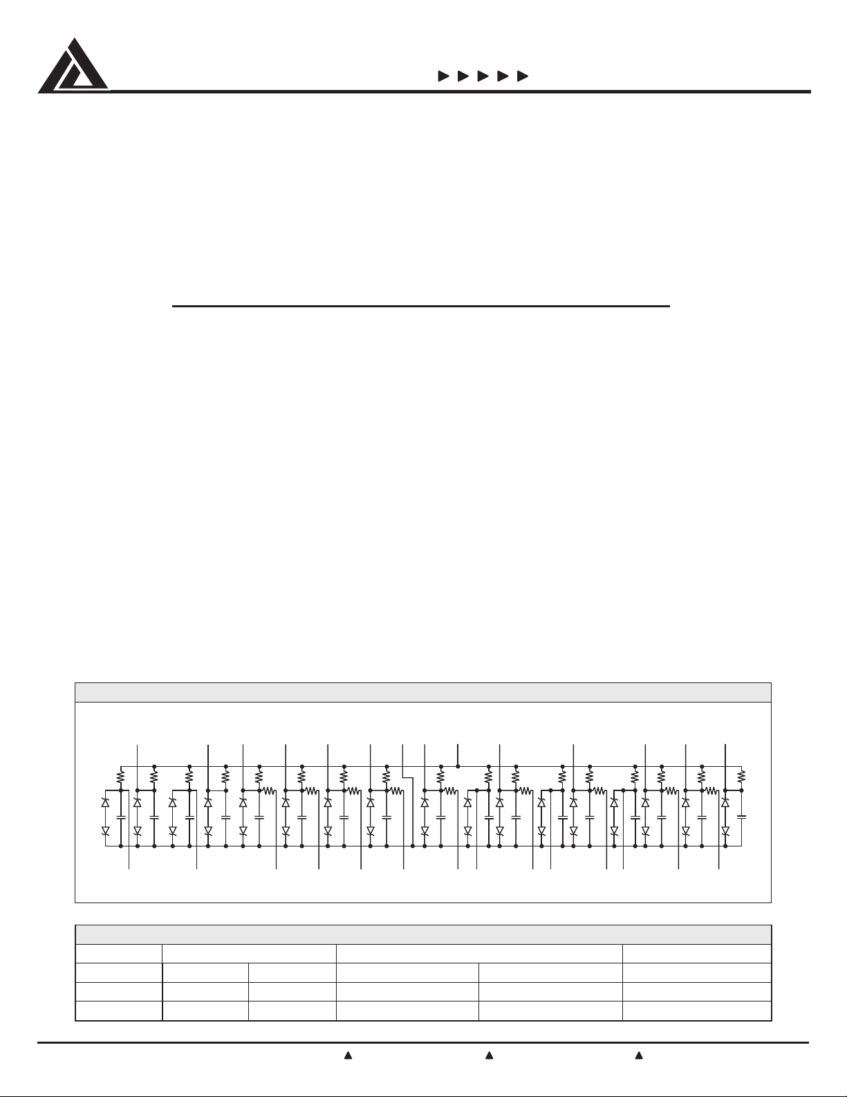
28
CC
1
27
26
R1R1R1R1
2
egakcaPrebmuNtraPgniredrO
edoCCRsniPelytSsebuTleeR&epaTgnikraMtraP
2082POSQT/Q20-4821SCAPR/Q20-4821SCAPQ204821SCAP
4082POSQT/Q40-4821SCAPR/Q40-4821SCAPQ404821SCAP
© 2000 California Micro Devices Corp. All rights reserved.
8/25/2000
215 Topaz Street, Milpitas, California 95035 Tel: (408) 263-3214 Fax: (408) 263-7846 www.calmicro.com
SCHEMATIC CONFIGURATION
21
V
CC
20
R1
R2
C
19
R1R1
R2
CCC
C
7
8
9
10
R1
R1
R2
C
C
11
12
1718
R1
R1
R2
C
C
13
16
15
R1
R1
R2
C
C
14
GND
22
25
R1
R2
C
3
24
R1
R2
C
4
23
R1
R1
R2
C
R2
C
5
6
NOITAMROFNIGNIREDROTRAPDRADNATS
C1420800
1
Page 2
CALIFORNIA MICRO DEVICES
PACS1284
SNOITACIFICEPSDRADNATS
)R(ecnareloTetulosbA%01±
)C(ecnareloTetulosbA%02±
egnaRerutarepmeTgnitarepOC°07otC°0
V
CC
rotsiseR/gnitaRrewoPWm001
tnerruCegakaeLmumixaM
Vta(
)xaM52@Aµ1C°
CC
:egatloVpmalClangiS
pmalCevitisoP
pmalCevitageN
erutarepmeTegarotSC°051otC°56–
gnitaRrewoPegakcaPxaM,W00.1
* Guaranteed by design
Note 1: Human Body Model per MIL-STD-883, Method 3015
C
ESD Contact Discharge from I/O pins 1, 2, 8, 10, 12, 15, 16, 17, 18, 19, 21, 23 through 28 to ground (pin22), one at a time.
Discharge
= 100pF, R
= 1.5 KΩ, pin 20 @ 5V and pin 22 @ ground.
Discharge
xaMV6
V6>
V6–<
*noitcetorPDSEniMxaM
)2etoN(MBH,noitcetorPmetsySnI VK8– VK8
SEULAVDRADNATS
(1R Ω)(2R Ω))fP(cedoCCR
K2.23302220
K7.43308140
SNOITACIFICEPSDSE
)1etoN(5103dohteM,ledoMydoBnamuH,O/IynataegatloVegrahcsiDkaeP VK4– VK4
)2,1etoN(2leveL,2-4-0001CEI,noitcetorPmetsySnI VK4– VK4
)2,1etoN(MBH,sesluPDSEVK8@egatloVpmalClennahC V03– V03
Note 2: Pin 22 grounded, pin 20 to V
pins 1, 2, 8, 10, 12, 15, 16, 17, 18, 19, 21, 23 through 28, one at a time.
Note 3: Standard IEC 1000-4-2 with C
, all other pins are open. ESD contact discharge between ground and
CC
Discharge
= 150pF, R
= 330Ω, pin 20 @ 5V and pin 22 @ ground.
Discharge
©2000 California Micro Devices Corp. All rights reserved.
2
215 Topaz Street, Milpitas, California 95035 Tel: (408) 263-3214 Fax: (408) 263-7846 www.calmicro.com
8/25/2000
Page 3

CALIFORNIA MICRO DEVICES
PACS1284
Application Information
The IEEE 1284 specification requires both termination and EMI filtering on a total of 17 signal lines. Control and
Status lines (8 in total) only require a pull-up resistor and a filter capacitor. The Data lines and Strobe also require a
series termination resistor in addition to the pull resistors and filter capacitors. See Table 1 and Schematic Diagram.
emaNlangiS
noitanimreTseireS
8ataD-1ataDseY
ebortSseY
tinIderiuqeRtoN
TXdeeFotuAderiuqeRtoN
nitceleSderiuqeRtoN
kcAderiuqeRtoN
ysuBderiuqeRtoN
ytpmErepaPderiuqeRtoN
tceleSderiuqeRtoN
tluaFderiuqeRtoN
Table 1.
IEEE 1284 defines three interface connectors:
• 1284-A is a 25-pin DB series connector which is the defacto PC standard for the host connection.
• 1284-B is a 36-pin, 0.085 inch centerline connector used on the peripheral device.
• 1284-C is a new 36-pin, 0.050 inch centerline connector which can be used for both host and peripheral.
Figure 1 shows a possible hook-up between the 1284-A connector on a PC motherboard and the PACS1284, illustrating how the pin configuration of the PACS1284 allows for easy interconnects between the two. The dotted I/O signals
of the PACS1284 will typically be connected to a Super I/O chip on the motherboard.
Figure 2 shows a possible hook-up between the 1284-B connector on a peripheral and the PACS1284.
Figure 3 shows a possible hook-up between the 1284-C connector and the PACS1284.
1284-A Connector
Host
14
1
SUPER 1284
1
Figure 1. Figure 2. Figure 3.
Sample Hook-ups of IEEE 1284 Connectors and PACS1284.
© 2000 California Micro Devices Corp. All rights reserved.
8/25/2000
215 Topaz Street, Milpitas, California 95035 Tel: (408) 263-3214 Fax: (408) 263-7846 www.calmicro.com
1284-B Connector
Peripheral
25
13
= FLOW
THROUGH
SIGNALS
19
1
SUPER 1284
1
36
18
= GND
=V
CC
(connector and PACS1284 not drawn to scale)
1284-C Connector
Host/Peripheral
20
19
2
1
SUPER 1284
1
36
18
3
Page 4

CALIFORNIA MICRO DEVICES
Table 2 defines the signals for the three connectors.
niP
rebmuN
1EBORTSEBORTSYSUB
21ataD1ataDtceleS
32ataD2ataDKCA
43ataD3ataDTLUAF
54ataD4ataDrorrEP
65ataD5ataD1ataD
76ataD6ataD2ataD
87ataD7ataD3ataD
98ataD8ataD4ataD
01KCAKCA5ataD
11YSUBYSUB6ataD
21rorrEProrrEP7ataD
31tceleStceleS8ataD
41DFOTUADFOTUATINI
51TLUAFdenifeDtoNEBORTS
61TINIdnuorGcigoLnitceleS
71nitceleSdnuorGsissahCDFOTUA
81dnuorGhgiHcigoLlarehpirePhgiHcigoLtsoH
91dnuorGdnuorGdnuorG
02dnuorGdnuorGdnuorG
12dnuorGdnuorGdnuorG
22dnuorGdnuorGdnuorG
32dnuorGdnuorGdnuorG
42dnuorGdnuorGdnuorG
52dnuorGdnuorGdnuorG
62dnuorGdnuorG
72dnuorGdnuorG
82dnuorGdnuorG
92dnuorGdnuorG
03dnuorGdnuorG
13TINIdnuorG
23TLULAFdnuorG
33denifeDtoNdnuorG
43denifeDtoNdnuorG
53denifeDtoNdnuorG
63nitceleShgiHcigoLlarehpireP
A-4821
PACS1284
stuoniProtcennoC4821EEEI
B-4821
busDnip-52
pmahCnip-63
CB-4821
ytisnedhgihnip-63
Table 2
When connecting a 1284-A host to a 1284-B peripheral the “Peripheral Logic High” signal is not used. Similarly, when
a 1284-A host is connected to a 1284-C peripheral the “Peripheral Logic High” and “Host Logic High” are not used.
These two signals are optionally used to detect a “Power Off” or “Cable Disconnect” state for host and peripheral
respectively.
©2000 California Micro Devices Corp. All rights reserved.
4
215 Topaz Street, Milpitas, California 95035 Tel: (408) 263-3214 Fax: (408) 263-7846 www.calmicro.com
8/25/2000
Page 5

CALIFORNIA MICRO DEVICES
PACS1284
Figure 4 shows typical Insertion Loss graphs for the PACS1284 for Data and Strobe signals. The curves are dependent on the physical location of the filter elements with respect to the ground and V
terminals of the device. These
CC
graphs are measured in a 50 Ohm environment. The signal is introduced at the series resistor input and the output is
measured at the corresponding filter capacitor. The graphs labeled A,B, and C are measured between 14 (input) and
16 (output), pin 3 (input) and 26 (output), and pin 6 (input) and 23 (output), respectively. The A graph depicts “worst
case” filter performance, while C represents a “best case” situation. Graphs of all other filter elements will fall in
between these two.
Sin dB
12
0
-10
A
-20
B
-30
-40
-50
300 450
C
600 750 900 1050 1200
(FREQUENCY, MHz)
Figure 4.
Typical Filter Insertion Loss for PACS1284 (S
Filter insertion loss is measured using Hewlett Packard HP 8753C Analyzer
in dB, TA = 25O C)
12
© 2000 California Micro Devices Corp. All rights reserved.
8/25/2000
215 Topaz Street, Milpitas, California 95035 Tel: (408) 263-3214 Fax: (408) 263-7846 www.calmicro.com
5
 Loading...