

Page 1
CALIFORNIA MICRO DEVICES
SNOITACIFICEPSDRADNATS
retemaraP.niM.pyT.xaM
egatloVylppuSgnitarepOV(
P
V-
N
)V5.5
@tnerruCylppuSV
P
V-
N
V5.5= Aµ02
I,egatloVdrawroFedoiD
F
C°52=T,Am02=V56.0V59.0
C°52=T,Am1@egatlovnwodkaerbesreverpmalcreneZ V6.6
noitcetorPDSE
metsys-ni,tupnIlennahCynataegatloVegrahcsiDkaeP
)2etoN(
000 5103dohteM,ledoMydoBnamuH
)4,3etoN(
±
VK51
000 2-4-00016CEIrepegrahcsiDtcatnoC
)5etoN(
±
VK8
C°52=T,MBHDSEVK51@egatloVpmalClennahC
)4,3setoN(
000stneisnartevitisoP
000stneisnartevitageN
V
P
+V0.31
V
N
-V0.31
C°52=T,tnerruCegakaeLlennahC Aµ1.0±Aµ0.1±
)zHM1@derusaeM(ecnaticapaCtupnIlennahC
V
P
V,V5=
N
,V0=V
TUPNI
V5.2=
)4etoN(
Fp3Fp6
gnitaRrewoPegakcaP
000egakcaPCIOS
000egakcaPPOSM
Wm053
Wm002
PAC DN016
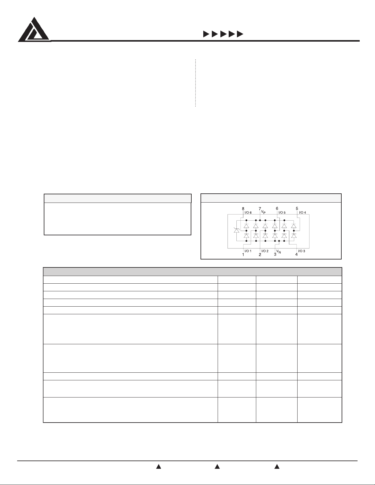
6 CHANNEL ESD PROTECTION ARRAY WITH ZENER SUPPLY CLAMP
Features
Six channels of ESD protection
Integral Zener diode clamp to suppress
supply rail transient
15KV ESD protection (HBM)
8KV contact, 15KV air ESD protection
per IEC 61000-4-2
Low loading capacitance, 3pF typ
Miniature 8-pin MSOP or SOIC package
Product Description
The PAC DN016 is a diode array designed to provide 6 channels of ESD protection for electronic components or sub-
systems. Each channel consists of a pair of diodes which steers the ESD current pulse either to the positive (V
negative (V
) supply. In addition, there is an integral Zener diode between V
N
disturbance due to these ESD current pulses. The PAC DN016 will protect against ESD pulses up to 15KV Human
Body Model, and 8KV contact discharge per International Standard IEC 61000-4-2.
This device is particularly well-suited for portable electronics (e.g. cellular phones, PDAs, notebook computers) because of
its small package footprint, high ESD protection level, and low loading capacitance. It is also suitable for protecting video
output lines and I/O ports in computers and peripheral equipment.
Applications
I/O port protection for cellular
phones, notebook computers, PDAs, etc.
ESD protection for VGA (Video) port in
PCs or Notebook computers.
ESD protection for sensitive
electronic equipment.
and VN to suppress any voltage
P
P
) or
ABSOLUTE MAXIMUM RATINGS
Diode Forward DC Current
Storage Temperature -65°C to 150°C
Operating Temperature Range -20°C to 85°C
DC Voltage at any Channel Input VN-0.5V to VP+0.5V
Note 1: Only one diode conducting at a time.
© 1999 Calirornia Micro Devices Corp. All rights reserved.
11/99
Note 2: From I/O pins to VP or VN only. Bypass opacitor between VP and VN is not required. However, a 0.2 µF ceramic chip
Note 3: Human Body Model per MIL-STD-883, Method 3015, C
Note 4: This parameter is guaranteed by design and characterization.
Note 5: Standard IEC 61000-4-2 with C
capacitor bypassing V
215 Topaz Street, Milpitas, California 95035 Tel: (408) 263-3214 Fax: (408) 263-7846 www.calmicro.com
SCHEMATIC CONFIGURATION
(Note 1) 20mA
to VN is recommended if the lowest possible channel clamp voltage is desired.
P
=150pF, and R
PAC is a trademark of California Micro Devices Corp.
Discharge
Discharge
=100pF, R
Discharge
=330Ω, VP=5V, VN=GND.
Discharge
=1.5KΩ, VP=5.0V, VN=GND.
C0540399
1
Page 2
CALIFORNIA MICRO DEVICES
)
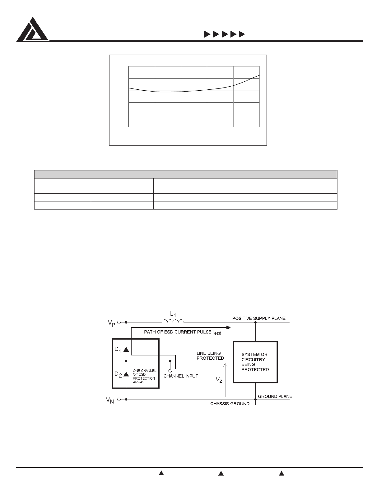
Input Capacita nce vs. Input Voltage
5
4
3
2
1
Input Capacitance (pF
0
012345
Input Voltage
Typical variation of CIN with VIN (VP=5V, VN=0V)
= 5V, V
(V
P
egakcaPrebmuNtraPgniredrO
sniPelytSgnikraMtraP
8CIOSS610NDCAP
8POSMM610NDCAP
When placing an order please specify desired shipping: Tubes or Tape & Reel.
= 0V, 0.1µF chip capacitor between V
N
& VN)
P
PAC DN016
NOITAMROFNIGNIREDROTRAPDRADNATS
Application Information
See also California Micro Devices Application note AP209, Design Considerations for ESD protection.
In order to realize the maximum protection against ESD pulses, care must be taken in the PCB layout to minimize parasitic
series inductances to the Supply and Ground rails. Refer to Figure 1, which illustrates the case of a positive ESD pulse
applied between an input channel and Chassis Ground. The parasitic series inductance back to the power supply is
represented by L1. The voltage VZ on the line being protected is:
V
= Forward voltage drop of D1 + L1 x d(I
Z
where I
is the ESD current pulse, and V
esd
)/dt + V
esd
is the positive supply voltage.
Supply
Supply
An ESD current pulse can rise from zero to its peak value in a very short time. As an example, a level 4 contact discharge per
the IEC 61000-4-2 standard results in a current pulse that rises from zero to 30 Amps in 1nS. Here d(I
approximated by ∆I
©1999 California Micro Devices Corp. All rights reserved.
2
215 Topaz Street, Milpitas, California 95035 Tel: (408) 263-3214 Fax: (408) 263-7846 www.calmicro.com
/∆t, or 30/(1x10
esd
Figure 1
)/dt can be
-9
). So just 10nH of series inductance (L1) will lead to a 300V increment in VZ!
esd
11/99
Page 3

CALIFORNIA MICRO DEVICES
PAC DN016
Similarly for negative ESD pulses, parasitic series inductance from the VN pin to the ground rail will lead to drastically increased
negative voltage on the line being protected.
Another consideration is the output impedance of the power supply for fast transient currents. Most power supplies exhibit a
much higher output impedance to fast transient current spikes. In the V
+ I
x R
by (V
DC
esd
), where VDC and R
out
power supply respectively. As an example, a R
are the nominal supply DC output voltage and effective output impedance of the
out
of 1 ohm would result in a 10V increment in VZ for a peak I
out
equation above, the V
Z
term, in reality, is given
Supply
of 10A.
esd
To mitigate these effects, a Zener diode has been integrated into this Protection Array between V
clamps the maximum voltage of V
it is recommended that V
P
channel clamp voltage, and is especially effective when V
relative to VN at the breakdown voltage of the Zener diode. Although not strictly necessary,
P
be bypassed to the ground plane with a high frequency bypass capacitor. This will lower the
is much lower than the Zener breakdown voltage. The value of this
P
and VN. This Zener diode
P
bypass capacitor should be chosen such that it will absorb the charge transferred by the ESD pulse with minimal change in V
Typically a value in the 0.1 µF to 0.2 µF range is adequate for IEC-61000-4-2 level 4 contact discharge protection (8KV). For
higher ESD voltages, the bypass capacitor should be increased accordingly. Ceramic chip capacitors mounted with short
printed circuit board traces are good choices for this application. Electrolytic capacitors should be avoided as they have poor
high frequency characteristics.
As a general rule, the ESD Protection Array should be located as close as possible to the point of entry of expected electrostatic
discharges. The power supply bypass capacitor mentioned above should be as close to the V
pin of the Protection Array as
P
possible, with minimum PCB trace lengths to the power supply and ground planes to minimize stray series inductance.
.
P
© 1999 Calirornia Micro Devices Corp. All rights reserved.
11/99
4
215 Topaz Street, Milpitas, California 95035 Tel: (408) 263-3214 Fax: (408) 263-7846 www.calmicro.com
Figure 5
8/99
 Loading...