

Page 1
PA7572 PEEL Array™
Programmable Electrically Erasable Logic Array
Commercial/Industrial
Versatile Logic Array Architecture
- 24 I/Os, 14 inputs, 60 registers/latches
- Up to 72 logic cell output functions
- PLA structure with true product-ter m sharing
- Logic functions and registers can be I/O-buried
High-Speed Commercial and Industrial Versions
- As fast as 13ns/20ns (tpdi/tpdx), 66.6MHz (f
-
Industrial grade available for 4.5 to 5.5V V
)
MAX
and -40
CC
to +85 °C temperatures
Ideal for Combinatorial, Synchronous and
Asynchronous Logic Applications
- Integration of multiple PLDs and random logic
- Buried counters, complex state-machines
- Comparators, decoders, other wide-gate functions
General Description
The PA7572 is a m ember of the Pr ogramm able Electr icall y
Erasable Logic (PEEL™) Array family based on ICT’s
CMOS EEPROM technology. PEEL™ Arrays free
designers from the limitations of ordinary PLDs by
providing the arc hitectural flexibilit y and speed needed for
today’s programm able logic designs. T he PA7572 offers a
versatile logic ar ray architecture with 2 4 I/O pins, 14 input
pins and 60 registers/ latche s ( 24 buried logic cells, 12 input
registers/latches, 24 buried I/O registers/latches). Its logic
array implements 100 sum-of-products logic functions
divided into two groups each serving 12 log ic cells. Each
group shares half (60) of the 120 product-terms available.
CMOS Electrically Erasable Technology
-
Reprogrammable in 40-pin DIP,
44-pin PLCC and TQFP packages
Flexible Logic Cell
- Up to 3 output functions per logic cell
- D,T and JK registers with special features
- Independent or global clocks, resets, presets,
clock polarity and output enables
- Sum-of-products logic for output enables
Development and Programmer Support
- ICT PLACE Development Software
- Fitters for ABEL, CUPL and other software
- Programming support by popular third-party
programmers
The PA7572’s logic and I/O cells (LCCs, IOCs) are
extremely flexible with u p to three output functi ons per cell
(a total of 72 for all 24 log ic c ells ) . Cel ls ar e configurable as
D, T, and JK registers with independent or global clocks,
resets, presets, cloc k polarity, and other features, m aking
the PA7572 suitable for a variety of combinatorial,
synchronous and asynchronous logic applications. The
PA7572 supports spee ds as fast as 13ns/20ns (tpdi/tpdx )
and 66.6MHz (f
) at moderate power consumption
MAX
140mA (100mA typical). Packaging includes 40-pin DIP
and 44-pin PLCC (see Figure 1). ICT and popular thirdparty development tool manufacturers provide
development and programming support for the PA7572.
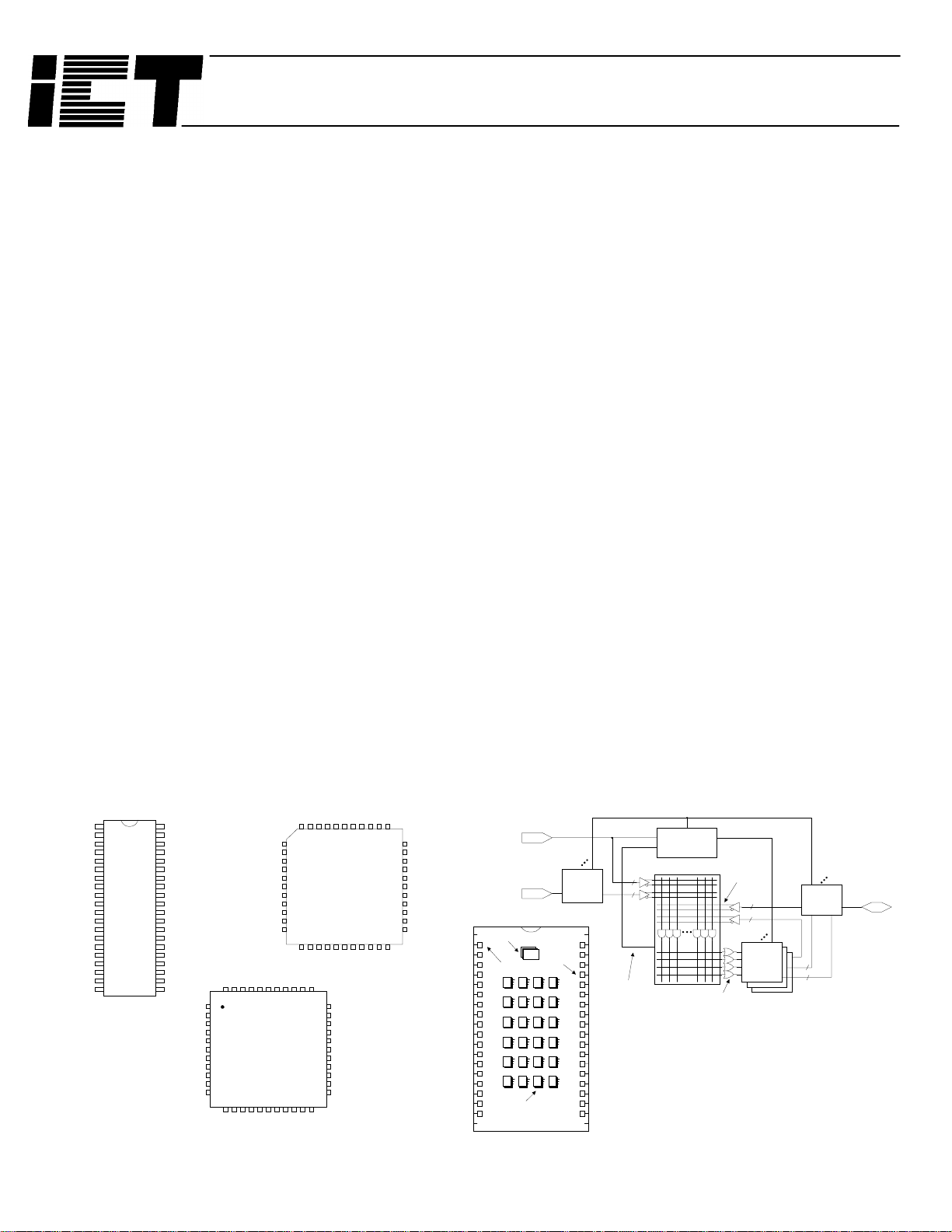
Figure 1. Pin Configuration
I/CL K 1
GND
I/O
I/O
I/O
I/O
I/O
I/O
I/O
I/O
I/O
I/O
I/O
I/O
DIP (600 mil)
1
I
2
I
3
I
4
5
6
7
8
9
10
11
12
13
14
15
16
I
17
I
18
I
19
20
40
39
38
37
36
35
34
33
32
31
30
29
28
27
26
25
24
23
22
21
TQFP
VCC
I
I
I
I/O
I/O
I/O
I/O
I/O
I/O
I/O
I/O
I/O
I/O
I/O
I/O
I
I
I
I/CL K 2
GND
I/O
I/O
I/O
I/O
I/O
I/O
I/O
I/O
I/O
I/O
1
2
3
4
5
6
7
8
9
10
11
12
I/O43I
44
13I14I15I16
I/O
42I41I40
PLCC
GND
I/CL K 1
39
GND17GND
I/O
I/O
I/O
I/O
I/O
I/O
I/O
I/O
I/O
I/O
VCC38VCC37I36I
18
19I20I21I22
I/CL K 2
7
8
9
10
11
12
13
14
15
16
17
I/O5I
6
18
19I20I21I22
I/O
35I34
4I3I2
I/O
33
32
31
30
29
28
27
26
25
24
23
I/O
GND
I/O
I/O
I/O
I/O
I/O
I/O
I/O
I/O
I/O
I/O
I/CL K 1
GND23GND
VCC44VCC43I42I
1
24
25I26I27I28
I/CL K 2
08-15-001A
41I40
Figure 2. Block Diagram
I/O
GND
39
I/O
38
I/O
37
I/O
36
I/O
35
I/O
34
I/O
33
I/O
32
I/O
31
I/O
30
I/O
29
I/O
I/CL K
I
I
I
I/O
I/O
I/O
I/O
I/O
I/O
I/O
I/O
I/O
I/O
I/O
I/O
I
I
I
2 Input/
Global Clock Pins
12 Input Pins
Global Cells
Input Cells
Logic Control Cells
PA7572
I/O C e l ls
Input
Cells
(INC)
VCC
I
I
I
I/O
I/O
I/O
I/O
I/O
I/O
I/O
I/O
I/O
I/O
I/O
I/O
I
I
I
I/CL K 2GND
2
12
4 sum terms
5 product term s
for Global Cells
Global
Cells
Logic
Array
124 (62X2)
Array Inputs
true and
complement
A
B
C
D
96 sum terms
(four per LC C )
I/O
24
24
Logic
Control
Cells
(LCC)
Cells
(IOC)
Buried
logic
24
24
24 Logic Control Cells
up to 3 output functions per cell
(72 total output functions
possible)
08-15-002A
24 I/O Pins
Logic
func tio ns
to I/O cells
1 04-02-050A
Page 2
Commercial/Industrial
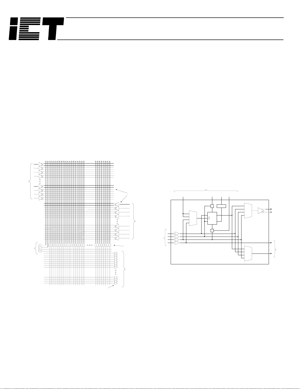
Inside the Logic Array
The heart of the P EEL™ Array architecture is based on a
logic array structur e s imilar to that of a PLA (programmable
AND, programmable OR). The logic array implements all
logic functions and provi des interconnection and contr ol of
the cells. In the PA7572 PEEL™ Array, 62 inputs are
available into the arra y from the I/O cells, inputs cells and
input/global-clock pins.
All inputs provide b oth true and c omplem ent signa ls, which
can be programm ed to any product term in the array. T he
PA7572 PEEL™ Arrays contains 124 product terms. All
product terms ( with the ex ception of c ertain ones f ed t o the
global cells) can be progr ammabl y connected to any of the
sum-terms of the logic control cells (four sum-terms per
logic control cell). Product-terms and sum-terms are also
routed to the global cells for control purposes. Figure 3
shows a detailed view of the logic array structure.
From
IO Cells
(IOC,INC,
I/CLK)
62 Array In puts
products functions pro vided to the logic c ells can be used f or
clocks, resets, presets and output enables instead of just
simple product-term control.
The PEEL™ logic array can also implement logic functions
with many product terms within a single-level delay. For
example a 16-bit c omparator ne eds 32 shared product term s
to implement 16 exclusive-OR functions. The PEEL™ logic
array easily handles this in a single level delay. Other
PLDs/CPLDs either run out of product-terms or require
expanders or additional logic levels that often slow
performance and skew timing.
Logic Control Cell (LCC)
Logic Control Cells (LCC) a re us ed t o a ll oc ate and c on trol th e
logic functions created in the logic array. Each L CC has four
primary inputs and thre e outputs . T he inputs t o each LCC are
complete sum-of - produc t logic f unc tions f rom the array, which
can be used to implem ent combinatoria l and sequential l ogic
functions, and to control LCC registers and I/O cell output
enables.
From G lobal Cell
Preset Reset
System C lock
RegType
From
Logic
Control
Cells
(LCC)
To
Global
Cells
PA7572 Logic Array
Figure 3. PA7572 Logic Array
True Product-Term Sharing
100 Sum Terms
125 Product
Terms
To
Logic Control
Cells
(LCC)
08-15-003A
The PEEL™ logic arra y provides several advantages over
common PLD logic arra ys. First, it allows for true pro ductterm sharing, not simply product-term steering, as commonly found in other CP LD s . Pr oduct ter m sharing ensures
that product-terms are used where they are needed and
not left unutilized or duplicated. Secondly, the sum-of-
From
Array
On/Off
P
Q
D,T,J
MUX
A
B
C
D
K
REG
R
MUX
MUX
08-15-004A
Figure 4. Logic Control Cell Block Diagram
As shown in Figure 4, the LCC is made up of three signal
routing multiplexer s and a versatile reg ister with s ynchronous
or asynchronous D, T , or JK registers (c locked-SR registers,
which are a subset of JK, are also possible). See Figure 5.
EEPROM memory cells are used for programming the
desired configuration. Four sum-of-product logic functions
(SUM terms A, B, C and D) are f ed into each LCC from the
logic array. Each SUM term can be selectively used for
multiple functions as listed below.
To
Array
To
I/O
Cell
2 04-02-050A
Page 3
Commercial/Industrial
Sum-A = D, T, J or Sum-A
Sum-B = Preset, K or Sum-B
Sum-C = Reset, Clock, Sum-C
Sum-D = Clock, Output Enable, Sum-D
D Register
Q = D after clocked
P
D
Q
Best for storage, simple counters,
shifters and state machines with
R
few hold (loop) conditions.
T Register
Q toggles when T = 1
P
Q
T
J
K
Q holds when T = 0
Best for wide binary counters (saves
R
product terms) and state machines
with many hold (loop) conditions.
JK Register
Q toggles when J/K = 1/1
P
Q
Q holds when J/K = 0/0
Q = 1 w h e n J/K = 1/0
Q = 0 w h e n J/K = 0/1
R
Combines features of both D and T
registers.
08-15-005A
Figure 5. LCC Register Types
SUM-A can serve as the D, T, or J input of the reg is ter or a
combinatorial pat h. SUM-B can s erve as th e K inp ut, or the
preset to the register , or a combinator ial path. SUM-C can
be the clock, the reset to the register, or a combinatorial
path. SUM-D can be the clock to the register, the output
enable for the connected I /O cell, or an internal feedback
node. Note that the sums controlling clocks, resets, presets
and output enables ar e co m plete sum -of- product f unctions,
not just product term s as with most other PLDs . This also
means that any inp ut or I/O pin can b e used as a cl ock or
other control function.
Several signals f rom the global cell are provided pr imarily
for synchronous (global) register control. The global cell
signals are routed to all LCCs. These signals include a
high-speed clock of positive or negative polarity, global
preset and reset, and a special register-type control that
selectively allo ws dynam ic switching of register type. This
last feature is especially useful for saving product terms
when implementing loa dable counters and state m achines
by dynamicall y switching from D-type register s to load and
T-type registers to count (see Figure 9).
Multiple Outputs Per Logic Cell
An important feature of the logic c ontrol cell is its c apabilit y
to have multiple output functions per cell, each operating
independently. As shown in Figure 4, two of the three
outputs can select the Q output from the register or the
Sum A, B or C combinatorial paths. Thus, one LCC output
can be registered, one c ombinatorial and the t hird, an output
enable, or an additional buried logic function. The multifunction PEEL™ Array logic cells are equivalent to two or
three macrocells of other PLDs, which have one output per
cell. They also allow regis ters to be truly buri ed from I/O pins
without limiting them to input-only (see Figure 8 & Figure 9).
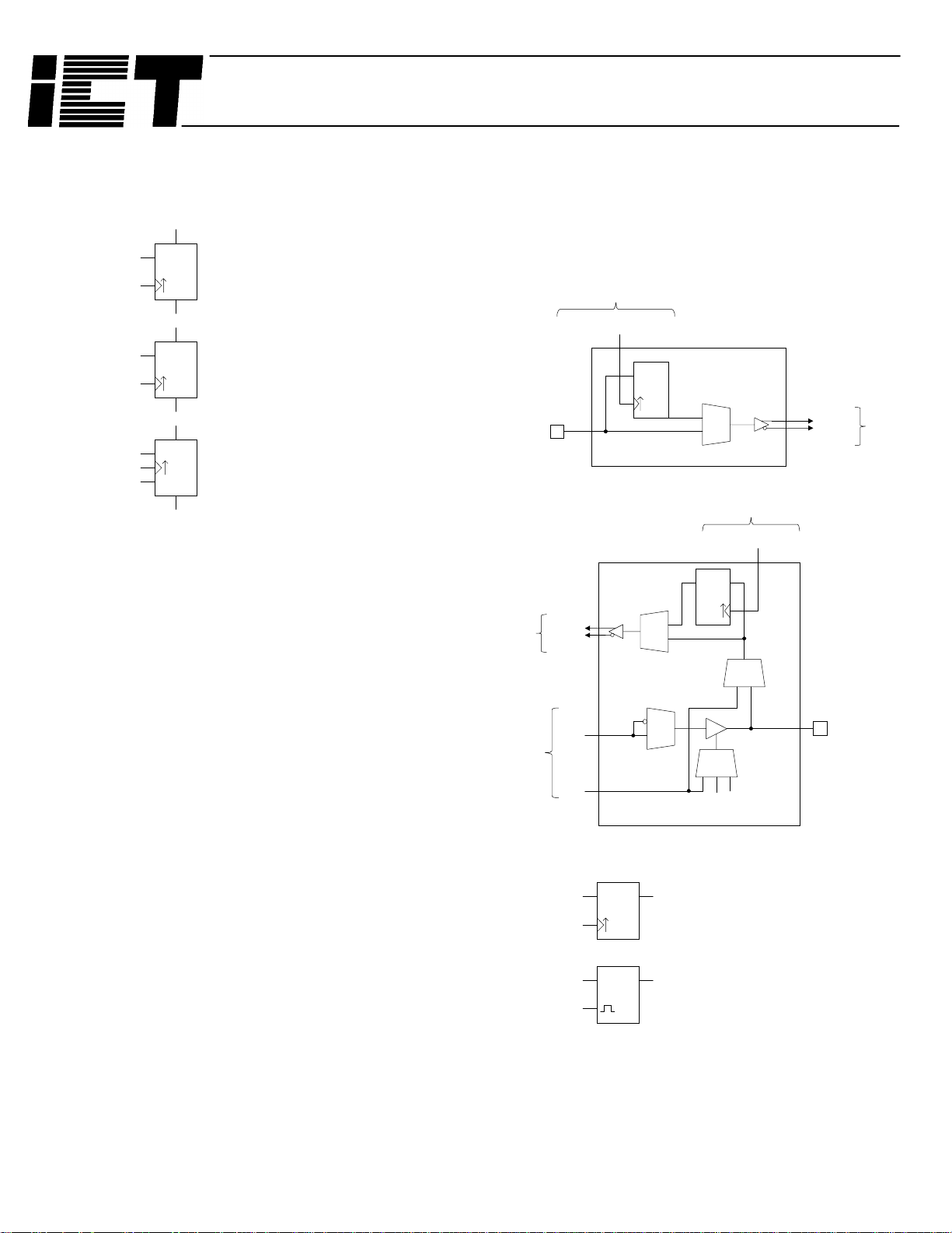
From Global Cell
Inpu t Cell Cloc k
REG/
Latch
Q
Inpu t
To
Array
From
Logic
Control
Cell
Inpu t
A,B,C
MUX
Inpu t Cell (IN C )
From Global Cell
Inpu t Cell Cloc k
REG/
Latch
Q
MUX
MUX
or
Q
D
MUX
I/O Cell (IO C)
MUX
1
0
Inpu t
08-15-006A
Figure 6. Input and I/O Cell Block Diagrams
D Q
LQ
IOC/INC Register
Q = D after rising edge of clock
holds until next rising edge
IOC /IN C La tc h
Q = L when clock is high
holds value when clock is low
08-15-007A
To
Array
I/O Pin
Figure 7. IOC/INC Register Configurations
3 04-02-050A
Page 4

Commercial/Industrial
Input Cells (INC)
Input cells (INC) are inc luded on dedica ted input pins . The
block diagram of the INC is shown in Figure 6. Each INC
consists of a multiplexer and a register/transparent latch,
which can be clock ed fr om various sourc es sel ected by th e
global cell (see Figure 7). The register is rising edge
clocked. The latch is transparent when the clock is high
and latched on the clock ’s falling edge. The register/ latch
can also be bypassed for a non-registered input.
I/O Cell (IOC)
All PEEL™ Arra ys have I/O cells ( IOC) as shown above in
Figure 6. Inputs to the IOCs can be fed from any of the
LCCs in the array. Each IOC cons ists of r outing an d contr ol
multiplexers, an input register/transparent latch, a threestate buffer and an output polarity control. The register/
latch can be clocked f rom a variety of sources determ ined
by the global cell. It can also be bypassed for a nonregistered input. T he PA7572 allows th e use of SUM-D as
a feedback to the array when the I/O pin is a dedicated
output. This allows f or additional buried r egisters and logic
paths. (See Figure 8 and Figure 9).
OE
QD
I/O
I/O wit h
independent
output enable
1
2
08-15-008A
Input with optional
register/latch
DQ
A
B
C
D
Global Cells
The global cells, sho wn in Figure 10 , are used to dir ect globa l
clock signals and/or control terms to the LCCs, IOCs and
INCs. The global cells allo w a clock to be selected from the
CLK1 pin, CLK2 pin, or a product term from the lo gic array
(PCLK). They also provide polarity control for INC and IOC
clocks enabling rising or falling clock edges for input
registers/latches. N ote that each individual LCC clock has its
own polarity control. T he global cell for LCCs include s sumof-products control term s for global reset and preset, and a
fast product term control for LCC regis ter-type, used to s ave
product terms for loada ble counters and s tate machines ( see
Figure 11). The PA75 72 provides two global cel ls that divide
the LCC and IOCs into groups, A and B. Half of the LCCs and
IOCs use global cell A, half use global cel l B. This means that
two high-speed global clocks can be used among the LCCs.
CLK1
CLK2
PCLK
CLK1
CLK2
PCLK
Reg-Type
Preset
Reset
Global Cell: LCC & IOC
MUX
Global Cell: INC
MUX
MUX
INC Clocks
Group A & B
LCC Clocks
IOC Clocks
LCC Reg-Type
LCC Presets
LCC Resets
08-15-010A
Figure 10. Global Cells
Reg-Type from Global Cell
Figure 8. LCC & IOC With Two Outputs
QD
Buried register or
logic paths
DQ
A
B
C
D
1
2
3
Output
08-15-009A
Figure 9. LCC & IOC With Three Outputs
Register Type Change Feature
P
D
R
P
T
R
Global Cell can dynam ically change user-
Q
selected LCC registers from D to T or from D
to JK. This saves product terms for loadable
counters or state machines. Use as D register
to load, use as T or JK to count. Timing
allows dynamic operation.
Example:
Product terms for 10 bit loadable binary counter
Q
D uses 57 product terms (47 count, 10 load)
T uses 30 product terms (10 count, 20 load)
D/T uses 20 product terms (10 count, 10 load)
08-15-011A
Figure 11. Register Type Change Feature
4 04-02-050A
Page 5

Commercial/Industrial
PEEL™ Array Development Support
Development support for PEEL™ Arrays is provided by
ICT and manufactur ers of popular developm ent tools. ICT
offers the powerful PL ACE Development Soft ware (free to
qualified PLD designers).
The PLACE software includes an architec tural editor, logic
compiler, waveform simulator, documentatio n utility and a
programmer interface. The PLACE editor graphically
illustrates and controls the PEEL™ Array’s architecture,
making the overall design easy to understand, while
allowing the eff ectivenes s of boolean logic equations, state
machine design and truth tabl e entr y. T he PLAC E co m piler
performs logic transformation and reduction, making it
possible to specify equat ions in almost any fashion and fit
the most logic possible in every design. PLACE also
provides a multi-le vel logic simulator allowing external and
internal signals to be simulated and analyzed via a
waveform display.(See Figure 12, Figure 13, Figure 14)
unexpected changes to be made quickly and without
waste. Programming of PEEL™ Arrays is supported by
many popular third party programmers.
Design Security and Signature Word
The PEEL™ Arrays provide a special EEPROM securit y bi t
that prevents unauthori zed reading or copying of designs.
Once set, the programmed bits of the PEEL™ Arrays
cannot be accessed until the entire chip has been
electrically erased. Another programming feature,
signature word, allows a user-definable code to be
programmed into the PEEL ™ Arra y. The code can be r ead
back even after the secur it y bit has been s et. T he s ign ature
word can be used to ident if y the patt ern pr o gr am med in the
device or to record the design revision.
Figure 12. PLACE Architectural Editor
PEEL™ Array development is also supported by popular
development tools, such as ABEL and CUPL, via ICT’s
PEEL™ Array fitter s. A special smart translator utility adds
the capability to directly convert JEDEC files for other
devices into equivalent JEDEC files for pin-compatible
PEEL™ Arrays.
Programming
PEEL™ Arrays are EE-reprogrammable in all package
types, plastic-DIP, PLCC and SOIC. This makes them an
ideal development vehicle for the lab. EEreprogrammability is also useful for production, allowing
5 04-02-050A
Figure 13. PLACE LCC and IOC Screen
Figure 14. PLACE Simulator Screen
Page 6

Commercial/Industrial
Table 1. Absolute Maximum Ratings
Symbol Parameter Conditions Ratings Unit
VCC Supply Voltage Relative to Ground -0.5 to + 7.0 V
VI, VO Voltage Applied to Any Pin Relative to Ground1 -0.5 to VCC + 0.6 V
IO Output Current Per pin (IOL, IOH) ±25 mA
TST Storage Temperature -65 to + 150 °C
TLT Lead Temperature Soldering 10 seconds +300 °C
Table 2. Operating Ranges
Symbol Parameter Conditions Min Max Unit
VCC Supply Voltage
TA Ambient Temperature
TR Clock Rise Time See Note 2 20 ns
TF Clock Fall Time See Note 2 20 ns
T
V
RVCC
Rise Time See Note 2 250 ms
CC
Table 3. D.C. Electrical Characteristics
Commercial 4.75 5.2
Industrial 4.5 5.5
Commercial 0 +70
Industrial -40 +85
Over the Operating Range
Symbol Parameter Conditions Min Max Unit
VOH Output HIGH Voltage - TTL VCC = Min, IOH = -4.0mA 2.4 V
V
OHC
VOL Output LOW Voltage - TTL VCC = Min, IOL = 16mA 0.5 V
V
OLC
VIH Input HIGH Level 2.0 VCC + 0.3 V
Output HIGH Voltage CMOS
Output LOW Voltage CMOS
V
= Min, IOH = -10µA VCC - 0.3 V
CC
V
= Min, IOL = -10µA 0.15 V
CC
V
°C
VIL Input LOW Level -0.3 0.8 V
IIL Input Leakage Current
IOZ Out put Leakage Current
ISC
11
I
V
CC
Output Short Circuit
4
Current
Current
CC
= Max, GND
V
CC
I/O = High-Z, GND
= 5V, VO = 0.5V, TA= 25°C -30 -120 mA
V
CC
V
= 0V or V
IN
f = 25MHz
All outputs disabled
7
C
IN
7
C
Output Capacitance5
OUT
Input Capacitance
5
T
= 25°C, VCC = 5.0V @ f = 1 M Hz
A
≤
≤
9
9
IN
CC
≤
≤
9
9
O
CC
3,11
CC
4
-20
I-20
6 04-02-050A
±10 µA
±10 µA
50 (typ.)
18
75
mA
85
6 pF
12 pF
Page 7

Commercial/Industrial
Table 4. A.C Electrical Characteristics Combinatorial
Symbol Parameter
t
PDI
t
PDX
t
t
AL
t
LC
t
LO
tOD, t
t
OX
IA
OE
Propagation delay Internal (tAL + tLC)
Propagation delay External (tIA + tAL +tLC + tLO)
Input or I/O pin to array input
Array input to LCC
LCC input to LCC output10
LCC output to output pin
Output Disable, Enable from LCC output7
Output Disable, Enable from input pin7
6,12
Over the Operating Range
-20/I-20
Min Max
13
20
12
20
2
1
5
5
Unit
ns
ns
ns
ns
ns
ns
ns
ns
This device has bee n designed and tes ted for the recom mended operating c onditions. Proper o peration outs ide of these
levels is not guaranteed. Exposure to absolute maximum ratings may cause permanent damage
Figure 15. Combinatorial Timing - Waveforms and Block Diagram
7 04-02-050A
Page 8

Table 5. A.C. Electrical Characteristics Sequential
COI
- LCC
14
+ tLO)
+ t
SCI
SCX
+ t
SCI
SCX
6,1
(tCK +tLC)
)
COI
+ t
COI
COX
+ t
COX
RTV
2
)
)
9
t
SCI
t
SCX
t
COI
t
COX
t
HX
t
SK
t
AK
t
HK
t
SI
t
HI
t
PK
t
SPI
t
HPI
t
SD
t
HD
t
SDP
t
HDP
t
CK
t
CW
f
MAX1
f
MAX2
f
MAX3
f
MAX4
f
TGL
t
PR
t
ST
t
AW
t
RT
t
RTV
t
RTC
t
RW
t
RESET
Symbol Parameter
Internal set-u p to sy s t em clock8 - LCC14
+ tSK + tLC - tCK)
(t
AL
Input16 (EXT.) set-up to system clock, - LCC (tIA + t
System-clock to Array Int. - LCC/IOC/INC
System-clock to Output Ext. - LCC (t
Input hold time from system clock - LCC
LCC Input set-up to async. clock
Clock at LCC or IOC - LCC output
LCC input hold time from system clock - LCC
Input set-up to system clock - IOC/INC14 (tSK - tCK)
Input hold time from system clock - IOC/INC (tSK - tCK)
Array input to IOC PCLK clock
Input set-up to PCLK clock17 - IOC/INC (tSK-tPK-tIA)
Input hold from PCLK clock17 - IOC/INC (tPK+tIA-tSK)
Input set-up to system clock - IOC/INC Sum-D
(
tIA + tAL + tLC + tSK - tCK)
Input hold time from system clock - IOC Sum-D
Input set-up to PCLK clock - IOC Sum-D15
+ tAL + tLC + tSK - tPK)
(t
IA
Input hold time from PCLK clock - IOC Sum-D
System-clock delay to LCC/IOC/INC
System-clock low or high pulse width
Max. system-clock frequency Int/Int 1/(t
Max. system-clock frequency Ext/Int 1/(t
Max. system-clock frequency Int/Ext 1/(t
Max. system-clock frequency Ext/Ext 1/(t
Max. system-clock toggle frequency 1/(tCW + tCW)
LCC presents/reset to LCC output
Input to Global Cell present/reset (tIA + tAL + tPR)
Asynch. preset/reset pulse width
Input to LCC Reg-Type (RT)
LCC Reg-Type to LCC output register change
Input to Global Cell register-type change (tRT + t
Asynch. Reg-Type pulse width
Power-on reset time for registers in clear state
13
Commercial/Industrial
-20/I-20
Min
8
SCI
)
10
0
1
1
4
0
5
10
10
0
0
7
0
7
)
8
)
10
Max
7
12
9
6
66.6
58.8
50.0
45.4
71.4
1
15
8
1
9
5
Unit
ns
ns
ns
ns
ns
ns
ns
ns
ns
ns
ns
ns
ns
ns
ns
ns
ns
ns
ns
MHz
MHz
MHz
MHz
MHz
ns
ns
ns
ns
ns
ns
ns
µs
8 04-02-050A
Page 9

Commercial/Industrial
Figure 16. Sequential Timing – Waveforms and Block Diagram
Notes
1. Minimum DC input is -0.5V, however inputs may under-shoot to -2.0V
2.Test points for Clock and V
3. I/O pins are 0V or V
4. Test one output at a time for a duration of less than 1 sec.
5. Capacitances are tested on a sample basis.
6. Test conditions assume: signal transition times of 5ns or less from the
7. t
8. DIP: “System-clock” refers to pin 1/21 hi gh speed clocks. PLCC: “Sys-
9. For T or JK registers in toggle (divide by 2) operation only.
10. For combinatorial and async-clock to LCC output delay.
11. ICC for a typical application: This parameter is tested with the device
12. Test loads are specified in Section 5 of this Data Book.
for periods less than 20ns.
10% and 90% levels.
10% and 90% points, timing reference levels of 1.5V (unless
otherwise specified).
OE
is measured from input transition to V
end of Section 6 for V
OH
-0.1V or V
to V
tem-clock” refers to pin 2/24 high speed clocks.
programmed as a 10-bit D-type counter.
OL
CC
.
REF
+0.1V.
CC
in tR,tF,tCL,tCH, and t
OD
value). t
is measured from input transition
are referenced at
RESET
±0.1V (See test loads at
REF
9 04-02-050A
13. “Async. Clock” refers to the clock from the Sum term (OR gate).
14. The “LCC” term indicates that the timing parameter is applied to the
LCC register. The “LCC/IOC” term indicates that the timing
parameter is applied to both the LCC and IOC registers. The
“LCC/IOC/INC” term indicates that the timing parameter is applied to
the LCC, IOC, and INC registers.
15. This refers to the Sum-D gate routed to the IOC register for an
additional buried register.
16. The term “input” without any reference to another term refers to an
(external) input pin.
17. The parameter t
is always slower than the data from the pin or input by the absolute
value of (t
from the pin or input is required, i.e. the external data and clock can
be sent to the device simultaneously. Additionally, the data from the
pin must remain stable for t
arrive at the IOC register.
18. Typical (typ) ICC is measured at T
5V
SK
indicates that the PCLK signal to the IOC register
SPI
-tPK -tIA). This means that no set-up time for the data
time, i.e. to wait for the PCLK signal to
HPI
= 25° C, freq = 25MHZ, VCC =
A
Page 10

Table 6. Ordering Information
Part Number Speed Temperature Package
PA7572P-20 P40
PA7572F-20 F44
PA7572J-20
PA7572PI-20 P40
PA7572FI-20
PA7572JI-20
13/20ns C
13/20ns
I
Figure 17. Part Number
De v ic e S u ffix
PA7572J-20
Commercial/Industrial
J44
F44
J44
Package
P = 600mil DIP
F = Thin Quad Flat Pack (TQFP)
J = Plastic (J) Leaded C hip Carrier (PLCC)
Speed
-20 = 13ns/20ns tpd/tpdx
Temperature Range
(Blank) = Com m ercial 0 to 70° C
I = Industrial -40 to +85° C
08-15-017A
Corporate Office
2123 Ringwood Avenue
San Jose, CA 95131
TEL (408) 434-0678
FAX (408) 432-0815
©2000 Integrated Circuit Technology Corp.
ICT reserves the right to make changes in specifications at any time and without notice. The information furnished by ICT
in this publication is believed to be accurate and reliable. However, no responsibility is assumed by ICT for its use nor for
any infringements of patents or other rights of third parties resulting from its use. No license is granted under any patents
or patent rights of ICT. ICT’s products are not authorized for use as critical components in life support devices or systems.
Marks bearing
©
or ™ are registered trademarks and trademarks of Integrated Circuit Technology Corp.
Email:
sales&marketing@ictpld.com
Website:
http://www.ictpld.com
10 04-02-050A
 Loading...