

Page 1
1 of 6
PA7140 PEEL
TM
Array
Programmable Electrica lly Erasable Logic Array
■
Versatile Logic Array Architecture
- 24 I/Os, 14 inputs, 60 registers/latches
- Up to 72 logic cell output functions
- PLA structure with true product-term sharing
- Logic functions and registers can be I/O-buried
■
High-Speed Commercial and Industrial Versions
- As fast as 13ns/20ns (tpdi/tpdx), 66.6MHz (f
MAX
)
- Industrial grade available for 4.5 to 5.5V Vcc and -40
to +85 °C temperatures Ideal for Combinatorial,
Synchronous and Asynchronous Logic Applications
- Integration of multiple PLDs and random logic
- Buried counters, complex state-machines
- Comparators, decoders, other wide-gate functions
■
CMOS Electrically Erasable Technology
-
Reprogrammable in 40-pin DIP,
44-pin PLCC, and TQFP packages
■
Flexible Logic Cell
- Up to 3 output functions per logic cell
- D,T and JK registers with special features
- Independent or global clocks, resets, presets,
clock polarity and output enables
- Sum-of-products logic for output enables
■
Development and Programmer Support
- ICT PLACE Development Software
-Fitters for ABEL, CUPL and other software
-Programming suppor t for by ICT PDS-3 and popular
third-party programmers
The PA7140 is a member of the Programmable Electrically
Erasable Logic (PEEL™) Array family based on ICT’s
CMOS EEPROM technology. PEEL™ Arrays free designers from the limitations of ordin ary PLDs by providing the
architectural flexibility and speed needed for today’s programmable logic designs. The PA7140 offers a versatile
logic array architecture with 24 I/O pins, 14 input pins and
60 registers/latches (24 buried logic cells, 12 input registers/latches, 24 buried I/O registers/latches). Its l ogic array
implements 100 sum-of-products logic functions divided
into two groups each serving 12 logic cells. Each group
shares half (60) of the 120 product-terms available for logic
cells.
The PA7140’s logic and I/O cells (LCCs, IOCs) are
extremely flexible with up to three output functions per cell
(a total of 72 for all 24 logic cells). Cells are configurable as
D, T, and JK registers with independent or global clocks,
resets, presets, clock polarity, and other features, making
the PA7140 suitable for a variety of combin atorial , synchronous and asynchronous logic applications. The PA7140
supports speeds as fast as 13ns/20ns (tpdi/tpdx) and
66.6MHz (f
MAX
) at moderate power consumption 140mA
(100mA typical). Packaging includes 40-pin DIP and 44-pin
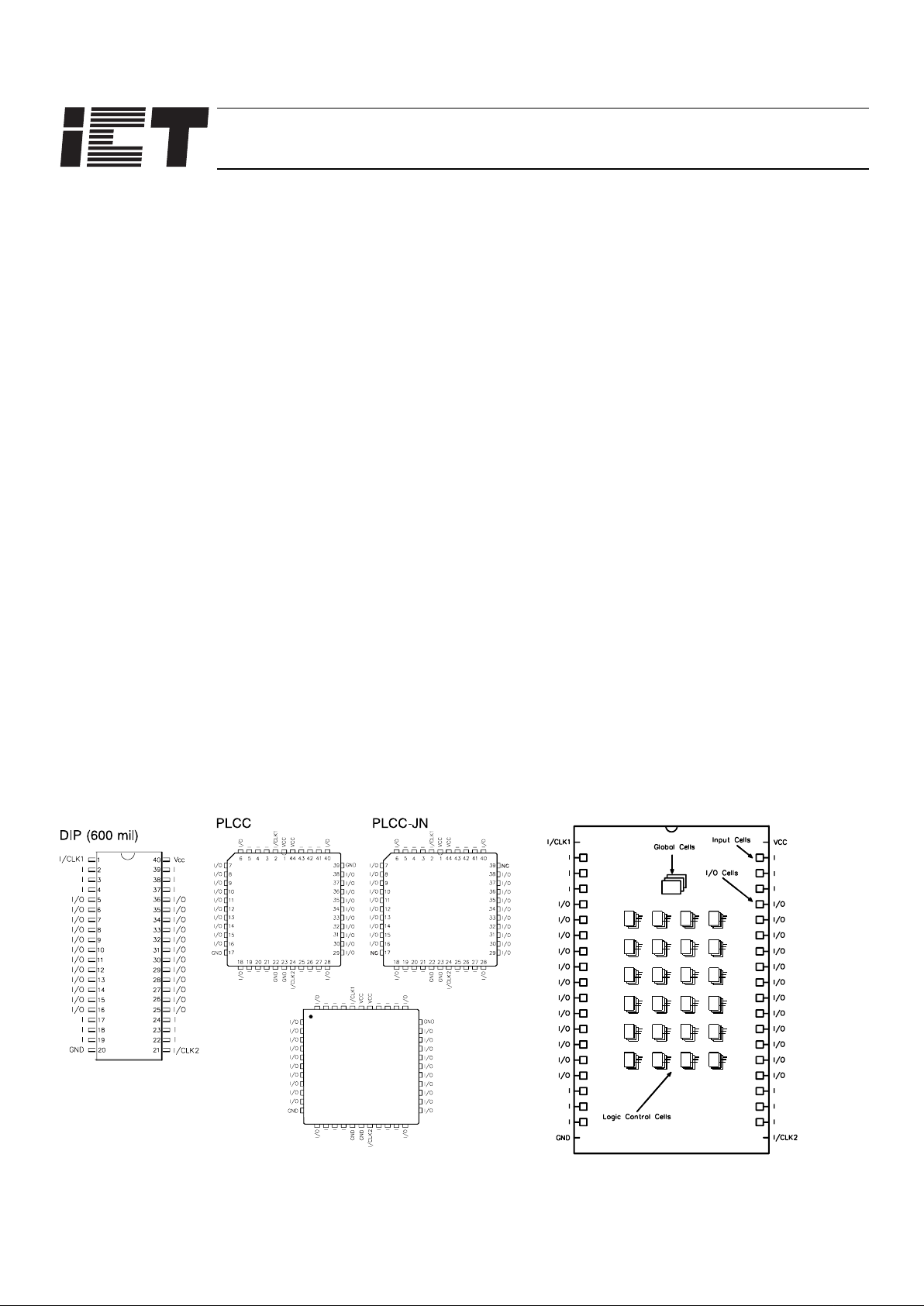
PLCC (see Figure 1). Development and programming support for the PA7140 is provided by ICT and popular thirdparty development tool manufacturers.
General Description
Features
TQFP
1
2
3
4
5
6
7
8
9
10
11
Pin 1
12 13 14 15 16 17 18 19 20 21 22
33
32
31
30
29
28
27
26
25
24
23
44 43 42 41 40 39 38 37 36 35 34
Figure 1: Pin Configuration Figure 2. Block Diagram
Commercial/
Industrial
Page 2
2 of 6
PA7140
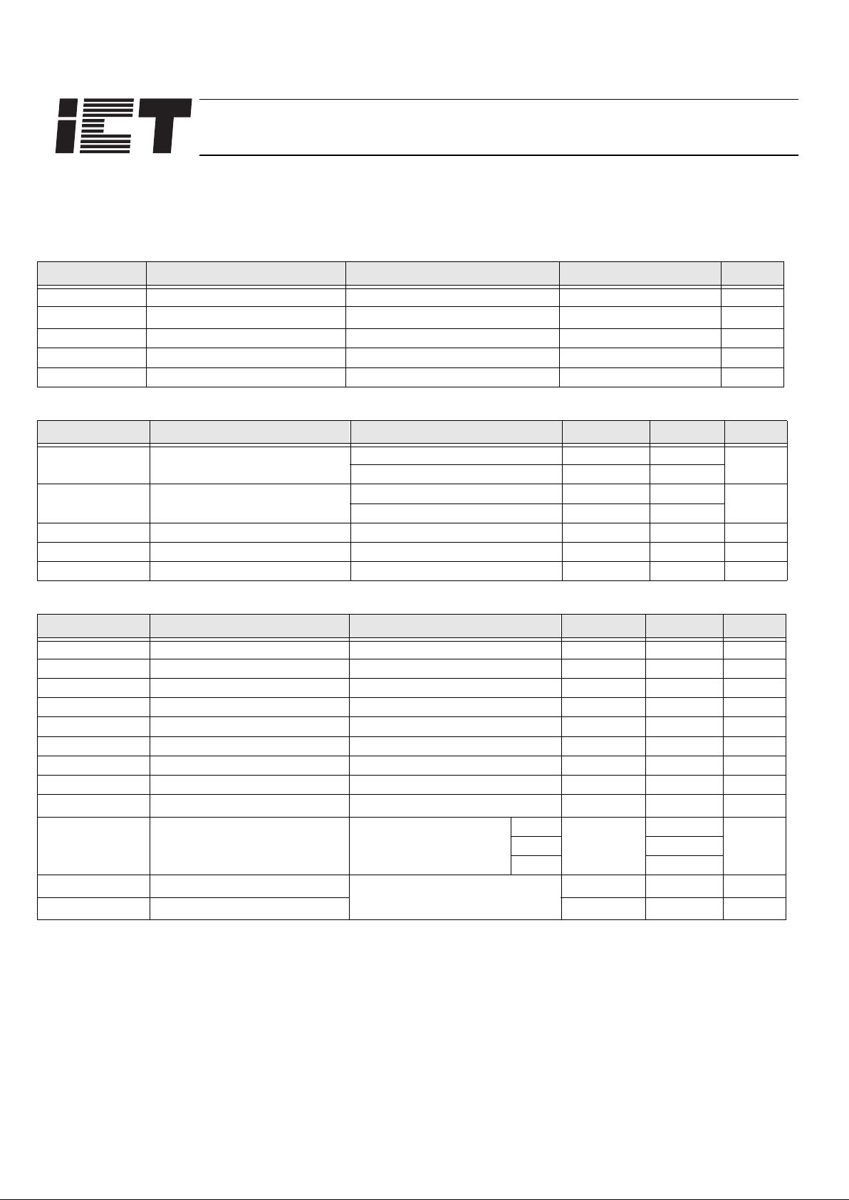
Table 1. Absolute Maximum Ratings
Symbol Parameter Conditions Ratings Unit
V
CC
Suppl y Voltage Relative t o Gr ou nd -0.5 to + 7.0 V
V
I
, V
O
Voltage Applied to Any Pin Relative to Ground
1
-0.5 to VCC + 0.6 V
I
O
Output Current Per pin (IOL, IOH)±25mA
T
ST
Storage Temperature -65 to + 150 °C
T
LT
Lead Temperature Soldering 10 seco nds +300 °C
Table 2. Operating Ranges
Symbol Parameter Conditions Min Max Unit
V
CC
Supply Voltage
Commercial 4.75 5.25
V
Industrial 4.5 5.5
T
A
Ambient Temperature
Commercial 0 +70
°C
Industrial -40 +85
T
R
Clock Rise Time See Note 2 20 ns
T
F
Clock Fall Time See Note 2 20 ns
T
RVCC
V
CC
Rise Time See Note 2 250 ms
Table 3. D.C. Electrical Characteristics over the recommended operating conditions
Symbol Parameter Conditions Min Max Unit
V
OH
Output HIGH Voltage - TTL VCC = Min, IOH = -4.0mA 2.4 V
V
OHC
Output HIGH Voltage - CMO S VCC = Min, IOH = -10µA VCC - 0.3 V
V
OL
Output LOW Voltage - TT L V
CC
= Min, I
OL
= 16mA 0.5 V
V
OLC
Output LOW Voltage - CM OS VCC = Min, IOL = -10µA 0.15 V
V
IH
Input HIGH Level 2.0 VCC + 0.3 V
V
IL
Input LOW Level -0.3 0.8 V
I
IL
Input Leakage Current V
CC
= Max, GND ≤ V
IN
≤
V
CC
±10 µA
I
OZ
Output Leakage Current I/O = High-Z, GND ≤ V
O
≤
V
CC
±10 µA
I
SC
Output Short Circuit Current
4
VCC = 5V, VO = 0.5V, TA= 25°C -30 -120 mA
ICC
11
VCC Current
V
IN
= 0V or V
CC
3,11
f = 25MHz
All outputs disabled
4
-20
100 (typ.)
18
140
mA-25 140
I-25 150
C
IN
7
Input Capacitance
5
TA = 25°C, VCC = 5.0V
@ f = 1 MHz
6pF
C
OUT
7
Output Capacitance
5
12 pF
This device has been designed and tested for the recommended
operating conditions. Proper operation outside of these levels is not
guaranteed. Exposure to absolute maximu m ratings may cause permanent damage.
Page 3

3 of 6
PA7140
Table 5. A.C Electrical Characteristics Combinatorial
Symbol Parameter
6,12
-20 -25 / I -25
UnitMin Max Min Max
t
PDI
Propagation delay Int e rnal (t
AL + tLC)
13 17 ns
t
PDX
Propagation delay External (tIA + tAL +tLC + tLO)2025ns
t
IA
Input or I/O pin to array input 2 2 ns
t
AL
Array input to LCC 12 16 ns
t
LC
LCC input to LCC output
10
11ns
t
LO
LCC output to output pin 5 6 ns
t
OD
, t
OE
Output Disable, Enable from LCC output
7
56ns
t
OX
Output Disable, Enable from input pin
7
20 25 ns
Combinatorial Timing - Waveforms and Block Diagram
Over the Operating Range
Page 4

4 of 6
PA7140
Table 1. A.C. Electrical Characteristics Sequential
Symbol Parameter
6,12
-20 -25 / I-25
Unit
Min Max Min Max
t
SCI
Internal set-up to system clock8 - LCC14
(t
AL
+ tSK + tLC - tCK)
811ns
t
SCX
Input
16
(EXT.) set-up to system clock, - LCC (t
IA + tSCI)
10 14 ns
t
COI
System-clock to Array Int. - LCC/IOC/INC
14
(t
CK +tLC
)
78ns
t
COX
System-clock to Output Ext. - LCC (t
COI
+ tLO)1214ns
t
HX
Input hold time from system cl ock - LCC 0 0 ns
t
SK
LCC Input set-up to async. clock
13
- LCC
11ns
t
AK
Clock at LCC or IOC - LCC output 1 1 ns
t
HK
LCC input hold time from syste m clock - LCC 4 4 ns
t
SI
Input set-up to system clock - IOC/INC14 (tSK - tCK)
00ns
t
HI
Input hold time from system clock - IOC/INC14 (tSK - tCK)
56ns
t
PK
Array input to IOC PCLK clock 9 11 ns
t
SPI
Input set-up to PCLK clock17 - IOC/INC (tSK-tPK-tIA)
00ns
t
HPI
Input hold from PCLK clock17 - IOC/INC (tPK+tIA-tSK)
10 12 ns
t
SD
Input set-up to system clock - IOC/INC Sum-D
15
(tIA + tAL + tLC + tSK - tCK)
10 13 ns
t
HD
Input hold time from system cl ock - IOC Su m-D 0 0 ns
t
SDP
Input set-up to PCLK clock
(t
IA
+ tAL + tLC + tSK - tPK) - IOC Sum-D
79ns
t
HDP
Input hold time from PCLK clock - IOC Sum-D 0 0 ns
t
CK
System-clock delay to LCC/IOCINC 6 7 ns
t
CW
System -clock low or high pulse width 7 8 ns
f
MAX
1 Max. system-clock frequency Int/Int 1/(t
SCI
+ t
COI
) 66.6 52.6 MHz
f
MAX
2 Max. system-clock frequency Ext/Int 1/(t
SCX
+ t
COI
) 58.8 45.4 MHz
f
MAX
3 Max. system-clock frequency Int/Ext 1/(t
SCI
+ t
COX
) 50.0 40.0 MHz
f
MAX
4 Max. system-clock frequency Ext/Ext 1/(t
SCX
+ t
COX
) 45.4 35.7 MHz
f
TGL
Max. system-clock toggle frequency 1/(tCW + tCW) 71.4 62.5 MHz
t
PR
LCC presents/reset to LCC output 1 2 ns
t
ST
Input to Global Cell present/reset (
tIA
+ tAL + tPR)1520ns
t
AW
Asynch . pr e se t /reset puls e w id t h 8 8 ns
t
RT
Input to LCC Reg-Type (RT) 8 10 ns
t
RTV
LCC Reg- Type to LCC outpu t re g is t er ch ange 1 2 ns
t
RTC
Input to Global Cell register-type change (tRT + t
RTV
)912ns
t
RW
Async h. Reg-Type pulse width 10 10 ns
t
RESET
Power-on reset time for registers in clear state
2
55µs
Over the Operating Range
Page 5

5 of 6
PA7140
Sequential Timing - Waveforms and Block Diagram
Notes
1. Mini mu m DC inpu t is - 0.5V, however in pu ts ma y u nd er -s hoo t to - 2 .0V f o r
periods less than 20ns.
2. Test points for Clock and V
CC
in tR,tF,tCL,tCH, and t
RESET
are referenced
at 10% and 90% levels.
3. I/O p ins are 0V or V
CC
.
4. Test one output at a time for a duration of less than 1 sec.
5. Capacitanc es are test ed on a sample basis.
6. Test conditions assume: signal transition times of 5ns or less from the
10% and 90% points, timing reference levels of 1.5V (unless otherwise
specified).
7. t
OE
is measured from input transition to V
REF
±0.1V (See test loads at
end of Secti on 6 for V
REF
value). t
OD
is measured from input tr ansition
to V
OH
-0.1V or V
OL
+0.1V.
8. DIP: “System-clock” refers to pin 1/21 high speed clocks. PLCC: “System-clock” refers to pin 2/24 high speed clocks.
9. For T or JK registers in toggle (divide by 2) operation only.
10. For combi natorial and async-clock to LCC output delay.
11. ICC for a typical application: Th is parameter is tested with the device
programmed as a 10-bit D-type counter.
12. Test loads are specified in Section 5 of this Data Book.
13. “Async. clock” refers to the clock from the Sum term (OR gate).
14. The “LCC” te rm indicates that the timing parame ter is applied to the
LCC register. The “IOC” term indicates that the timing parameter is
applied to the IOC register. The “LCC/IOC” term indicates that the timing parameter is applied to both t he LCC and IOC register s. The “ LCC/
IOC/INC” term indicates that the timing parameter is applied to the
LCC , IOC and INC registers.
15. Thi s refers to th e Sum-D gate routed to the IOC register f or an additional buried register
16. The term “Input” without any referenc e to another term refers to an
(external) input pin.
17. Th e p ar am e ter t
SPI
indicates that the PCLK signal to the IOC register is
always slower than the data from the pin or input by the absolute value
of (t
SK -tPK -tIA
). This means that no set-up time for the data from the
pin or input is requir ed, i.e. the external data and clock can be sent to
the device simultan eously. Additionally, the data from the pin must
remain stable for t
HPI
time, i.e. to wait for the PCLK signal to arrive at
the IOC regist er.
18. Typical ( typ) ICC is measured at T
A
=25° C, Freq = 25MHz, V
CC
=5V.
Page 6

6 of 6
PA7140
Table 5. Ordering Information
Part Number Speed Temperature Package
PA7140P-20
13/20ns C
P40
PA7140F-20 F44
PA7140J-20 J44
PA7140JN-20 JN44
PA7140P-25
17/25ns
CP40
PA7140PI-25 I P40
PA7140F-25
17/25ns
CF44
PA7140FI-25 I F4 4
PA7140J-25
17/25ns
CJ44
PA7140JI-25 I J4 4
PA7140JN-25
17/25ns
CJN44
PA7140JNI-25 I JN4 4
Part Number
Device
PA 7140J -20
Package
P = Plastic 600mil DIP
F= Thin Quad Flat Pack (TQFP)
J = Plastic (J) Leaded Chip Carrier
JN = Alternate pin- out PLCC
Temperature Range
(Blank) = Commercial 0 to 70°C
I = Industrial -40 to +85°C
Speed
-20 = 13ns/20ns tpdi/tpdx
-25 = 17ns/25ns tpdi/tpdx
Suffix
 Loading...