

Page 1

INTEGRATED CIRCUITS
DATA SH EET
P90CE201
16-bit microcontroller
Product specification
File under Integrated Circuits, IC21
August 1993
Page 2

Philips Semiconductors Product specification
16-bit microcontroller P90CE201
CONTENTS
1 FEATURES
2 GENERAL DESCRIPTION
3 ORDERING INFORMATION
4 PINNING INFORMATION
4.1 Pinning
4.2 Pin description
5 CPU FUNCTIONAL DESCRIPTION
5.1 General
5.2 5.2 Programming model and data organization
5.3 Internal and external operation
5.4 Processing states and exception processing
5.5 Stack format
5.6 CPU interrupt processing
6 SYSTEM CONTROL
6.1 Memory mapping
6.2 Interrupt controller
6.3 System Control Registers
6.4 Reset
6.5 Clock circuitry
7 INSTRUCTION SET
7.1 Addressing modes
7.2 Instruction timing
8I
8.1 General
8.2 I2C-bus interface registers
9 UART SERIAL INTERFACE
9.1 General
9.2 Operating modes
9.3 UART registers
2
C-BUS INTERFACE
10 8-BIT GENERAL PORT
10.1 8-bit General Port registers
11 8-BIT AUXILIARY PORT
11.1 8-bit Auxiliary Port registers
12 WATCHDOG TIMER
13 TIMERS
13.1 General
13.2 Timer operating modes
13.3 Timer registers
14 ELECTROMAGNETIC COMPATIBILITY
(EMC) IMPROVEMENTS
15 ELECTRICAL SPECIFICATIONS
15.1 Limiting values
15.2 DC Characteristics
15.3 AC Characteristics
16 REGISTER MAP
17 PACKAGE OUTLINE
18 SOLDERING
18.1 Introduction
18.2 Reflow soldering
18.3 Wave soldering
18.4 Repairing soldered joints
19 DEFINITIONS
20 LIFE SUPPORT APPLICATIONS
21 PURCHASE OF PHILIPS I2C COMPONENTS
August 1993 2
Page 3

Philips Semiconductors Product specification
16-bit microcontroller P90CE201
1 FEATURES
• CMOS technology
• Full 68000 software compatibility
• 32-bit internal structure
• 16-bit internal data transfer
• 8-bit access to external ROM/RAM
• External addressing range 16 Mbytes for ROM and
16 Mbytes for RAM
• Unused address pins can be used as quasi-bidirectional
ports
• On-chip address decoder for ROM/RAM
• 8 edge triggered programmable interrupts that can also
be used as quasi-bidirectional ports
• Reset control
• Built-in clock generator
2
• 2 fully independent fast I
• UART serial interface (4 modes)
• 3 fully independent 16-bit timers
• Watchdog timer
• 8-bit quasi-bidirectional port, 4-bits with high drive
capability
• EMC optimized layout and pinning
• 64-pin QFP package
C-bus serial interfaces
2 GENERAL DESCRIPTION
The P90CE201 is a member of the P9XCXXX family of
highly integrated 16-bit microcontrollers for use in a wide
variety of applications. It is fully software compatible with
the 68070/68000. The complete set of system functions
available on the chip results in reduced system cost.
Additionally, its modular design concept permits future
extension to the family.
3 ORDERING INFORMATION
EXTENDED
TYPE NUMBER
P90CE201AEB 64 QFP plastic SOT319
Note
1. SOT319-2; 1996 November 28.
August 1993 3
PINS PIN POSITION MATERIAL CODE
PACKAGE CLOCK
FREQUENCY
(1)
TEMPERATURE RANGE
(MHz)
24.0 −25 to 85
(°C)
Page 4
Philips Semiconductors Product specification
16-bit microcontroller P90CE201
RESET
XTAL1
XTAL2
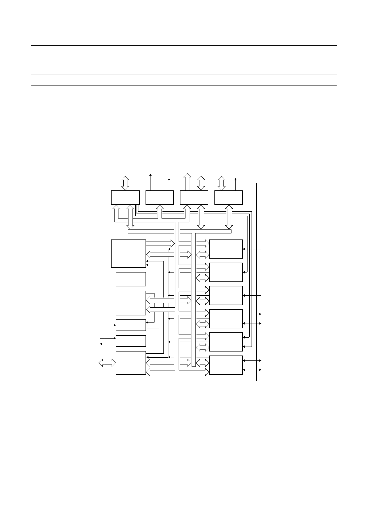
GP0-GP7
(1)
PORT
CPU
SYSTEM
CONTROL
WATCHDOG
TIMER
RESET
LOGIC
CLOCK
CSRAMN
ADDRESS
DECODER
CSROMN
OCA (31 : 0)
A0-A15
ADDRESS
BUFFER
A16-A23
D0-D7
INTERFACE
OCD (15 : 0)
TIMER 0
TIMER 1
TIMER 2
UART
I C 1
R/WN
DATA
T0
T2
TXD
RXD
2
INTN0 INTN7
INTERRUPT
CONTROLLER
1. The General Port lines GP5, GP6 and GP7 have alternate functions for Timer 1, SCL1 and SDA1
respectively; see Table 1.
Fig.1 Block diagram
August 1993 4
2
I C 2
SCL2
SDA2
MLB015
Page 5
Philips Semiconductors Product specification
16-bit microcontroller P90CE201
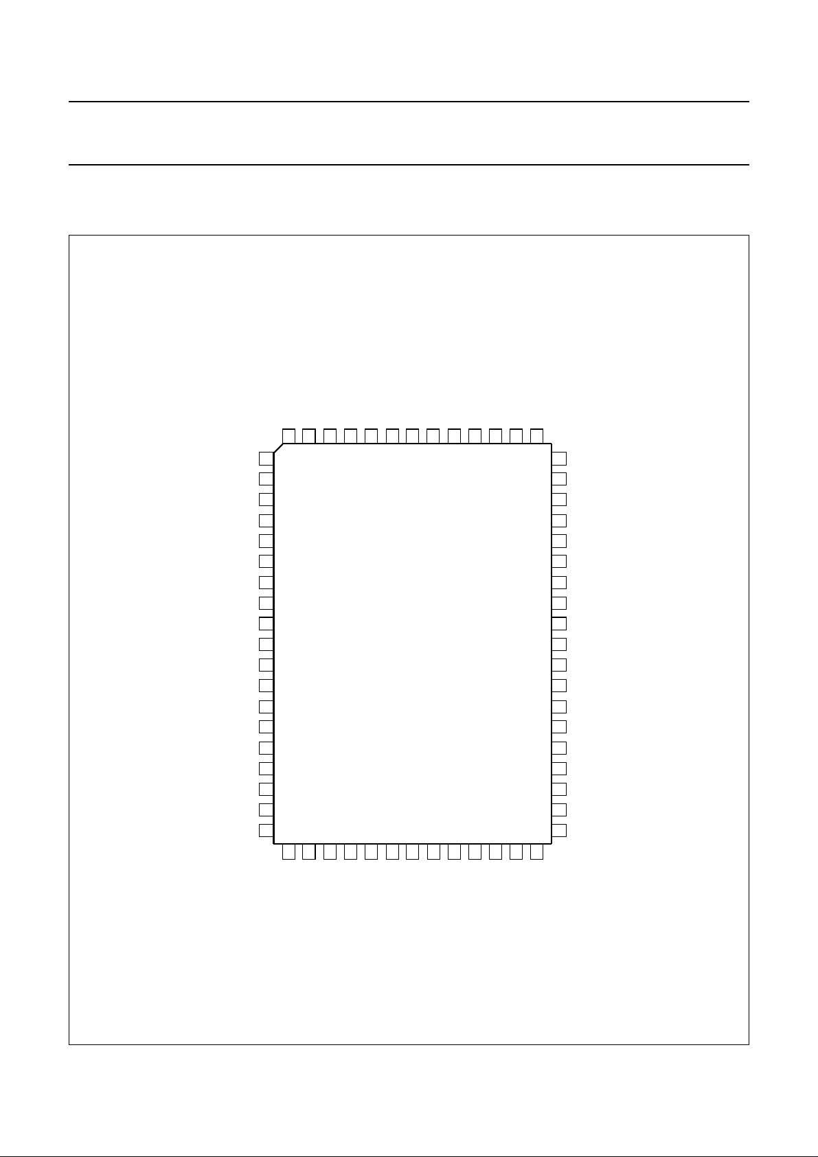
4 PINNING INFORMATION
4.1 Pinning
DD2
V
RESET
T0
27
T2
LP0/INTN0
56
55
28
29
A7
A13
54
53
52
V
51
SS2
CSRAMN
50
49
D3
48
D2
47
D4
46
D1
45
D5
44
D0
43
D6
42
A0
D7
41
40
A1
39
A2
38
A10
A3
37
CSROMN
36
35
A4
34
A11
33
A5
30
31
32
A8
A6
MLB003
A9
handbook, full pagewidth
RXD
SDA2
SCL2
GP7/SDA1
GP6/SCL1
GP0
GP1
GP2
GP3
GP4
GP5/T1
A23/AP7
A22/AP6
A21/AP5
A20/AP4
XTAL2
XTAL1
V
DD1
V
SS1
TXD
LP6/INTN6
LP7/INTN7
64
63
62
1
2
3
4
5
6
7
8
9
10
11
12
13
14
15
16
17
18
19
20
21
R/WN
A19/AP3
LP5/INTN5
61
22
23
A18/AP2
A16/AP0
LP4/INTN4
60
P90CE201
24
A17/AP1
LP2/INTN2
LP3/INTN3
59
58
25
26
A15
A14
LP1/INTN1
57
A12
Fig.2 Pin configuration for QFP64.
August 1993 5
Page 6

Philips Semiconductors Product specification
16-bit microcontroller P90CE201
4.2 Pin description
Table 1 QFP64 package.
MNEMONIC TYPE PIN NO. FUNCTION
RXD I/O 1 Receive Data. RXD is the data input for the UART interface.
SDA2 I/O 2 Serial Data 2 (open drain). SDA2 is the data signal for the second
SCL2 I/O 3 Serial Clock 2 (open drain). SCL2 is the clock signal for the second
GP7/SDA1
GP6/SCL1
GP0
GP1
GP2
GP3
GP4
GP5/T1
A23/AP7
to
I/O 4
5
6
7
8
9
10
11
I/O 12 to 15, 21,
22, 24, 23
A16/AP0
A15 to A0 O 25, 26, 28, 27,
34, 38, 32, 30,
29, 31, 33, 35,
37, 39, 40, 42
XTAL2 O 16 Oscillator output. Not connected if an external clock generator is used.
XTAL1 I 17 Oscillator input. XTAL1 can also be used as an external clock input if
V
V
DD1
SS1
− 18 Supply voltage. For internal logic, address bus, data bus, RWN,
− 19 Ground. For internal logic, address bus, data bus, RWN, CSRAMN,
R/WN O 20 Read (active HIGH)/Write (active LOW). This controls the direction of
CSROMN O 36 Chip Select ROM (active LOW). This signal selects external ROM.
D0 to D7 O 44, 46, 48, 49,
47, 45, 43, 41
CSRAMN O 50 Chip Select RAM (active LOW). This signal enables external RAM.
V
V
SS2
DD2
− 51 Ground. For all other periphery pins (quiet port).
− 52 Supply voltage. For all other periphery pins (quiet port).
RESET I 53 Reset (active HIGH). Input pin for an external reset.
T0 I 54 Timer 0. Input pin for cycle and event counting using Timer 0.
T2 I 55 Timer 2. Input pin for cycle and event counting using Timer 2.
2
I
C-bus serial interface.
2
C-bus serial interface.
I
General Purpose Port (active HIGH, 3-state). The alternative functions
are as follows. SCL1 is the clock signal for the first I
2
C-bus serial
interface. SDA1 is the data signal for the first I2C-bus serial interface.
T1 is the input pin for Timer 1.
Address Bus. Upper 8-bits of the address bus (A23 to A16). The unused
address bits can be selected as a quasi-bidirectional port (AP).
Address Bus. Lower 16-bits of the address bus.
an external clock generator is used.
CSRAMN, CSROMN, XTAL1 and XTAL2.
CSROMN, XTAL1 and XTAL2.
data flow.
Data Bus. 8-bit data bus.
August 1993 6
Page 7

Philips Semiconductors Product specification
16-bit microcontroller P90CE201
MNEMONIC TYPE PIN NO. FUNCTION
LP0/INTN0
LP1/INTN1
LP2/INTN2
LP3/INTN3
LP4/INTN4
LP5/INTN5
LP6/INTN6
LP7/INTN7
TXD O 64 Transmit Data. TXD is the data output for the UART serial interface.
I/O 56
57
58
59
60
61
62
63
Latched Interrupt inputs (active LOW). A LOW level of ≥ 1 clock pulse
will be stored as a pending interrupt request. Priority levels are
programmable. Unused interrupt inputs can be used as a
quasi-bidirectional port (LP).
August 1993 7
Page 8

Philips Semiconductors Product specification
16-bit microcontroller P90CE201
5 CPU FUNCTIONAL DESCRIPTION
5.1 General
The CPU of the P90CE201 is software compatible with the
68000, consequently programs written for the 68000 will
run on the P90CE201 unchanged. However, for certain
applications the following differences between the
processors should be noted:
• The initialization of the System Control Registers.
• Differences exist in the address error exception
processing since the P90CE201 can provide full error
recovery.
• The timing is different because of the P90CE201’s new
architecture and technology. The instruction execution
timing is completely different for the same reason.
31 16 15 8 7 0
handbook, full pagewidth
5.2 5.2 Programming model and data organization
The programming model is identical to that of the 68000
and is shown in Fig.3. It contains seventeen 32-bit
registers, a 32-bit Program Counter and a 16-bit Status
Register. The first eight registers (D0 to D7) are used as
data registers for byte, word and long-word operations.
The second group of registers (A0 to A6) and the System
Stack Pointer (A7) can be used as software stack pointers
and base address registers. In addition, these registers
can be used for word and long-word address operations.
All seventeen registers can be used as Index Registers.
The P90CE201 supports 8, 16 and 32-bit integer data,
BCD data 32-bit addresses. Each data type is arranged in
memory as shown in Fig.4.
DO
D1
D2
Eight
D3
Data
D4
Registers
D5
D6
D7
31 16 15 0
USER STACK POINTER
SUPERVISOR STACK POINTER
31 0
MCD504
Fig.3 Programming model.
August 1993 8
15 8 7 0
SYSTEM
BYTE
USER
BYTE
A0
A1
A2
A3
A4
A5
A6
A7
Seven
Address
Registers
Two Stack
Pointers
Program
Counter
Status
Register
Page 9
Philips Semiconductors Product specification
16-bit microcontroller P90CE201
bit
(a) Bit data (1 Byte = 8 bits).
15 14 13 12 11 10 9 8 7 6 5 4 3 2 1 0bit
MSB BYTE 0
BYTE 2
(b) Integer data (1 Byte = 8 bits).
1514131211109876543210bit
MSB WORD 0
(c) Word data (16 bits).
1514131211109876543210bit
MSB HIGH ORDER
LONG WORD 0
LONG WORD 1
LONG WORD 2
(d) Long-word data (32 bits).
276543 1 0
LSB
WORD 1
WORD 2
BYTE 1
BYTE 3
LOW ORDER LSB
HIGH ORDER
LOW ORDER
HIGH ORDER
LOW ORDER
LSB
1514131211109876543210bit
MSB HIGH ORDER
1514131211109876543210bit
MSB LSB
ADDRESS 0
ADDRESS 1
ADDRESS 2
(e) Addresses (1 address =32 bits).
BCD 0 BCD 1
BCD 4 BCD 5
(f) BCD data (2 BCD digits = 1 Byte).
LOW ORDER LSB
HIGH ORDER
LOW ORDER
HIGH ORDER
LOW ORDER
Fig.4 Memory data organization.
August 1993 9
BCD 2 BCD 3
BCD 6 BCD 7
MCD505
Page 10

Philips Semiconductors Product specification
16-bit microcontroller P90CE201
handbook, full pagewidth
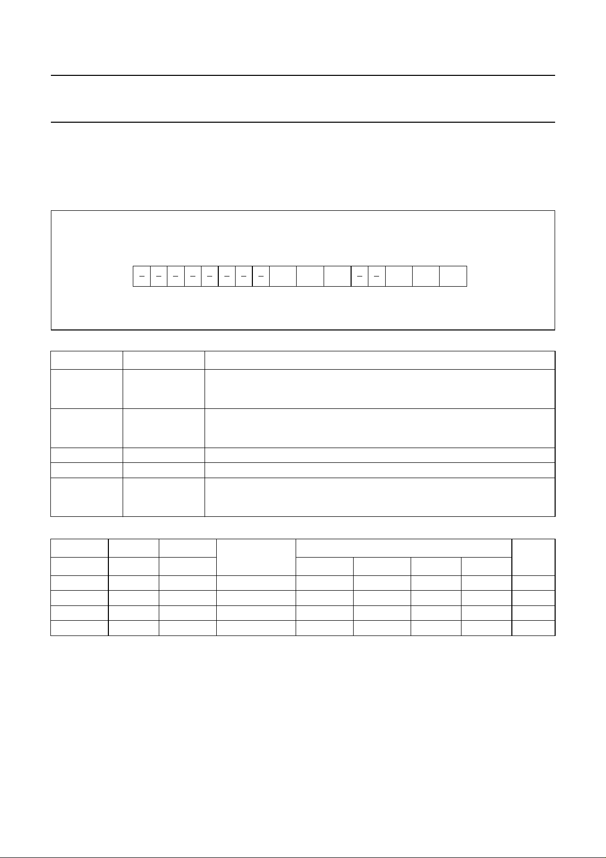
T – S – – 121110 – – – X N Z V C
Trace
Mode
Supervisor
State
Interrupt
Mask
Fig.5 Status Register.
5.3 Internal and external operation
The P90CE201 operates with an internal clock frequency
of half the oscillator frequency (f
/2). Each internal clock
OSC
cycle is divided into 2 states. A non-access machine cycle
has 3 clock cycles or 6 states (S0 to S5). A minimum bus
cycle normally consists of 3 clock cycles (6 states). When
data transfer has not yet been terminated, wait states (SW)
are inserted in multiples of 2. For external memory access,
2 wait states (bus states SB) are added automatically.
5.4 Processing states and exception processing
The CPU is always in one of three processing states:
normal, exception or halted.
The normal processing state is that associated with
instruction execution; the memory references are to fetch
instructions and operands and to store results. A special
case of the normal state is the stopped state which the
processor enters when a STOP instruction is executed. In
this state the CPU makes no further memory references.
048101315BIT
Carry
Overflow
Zero
Negative
Extend
MCD506
The halted processing state is an indication of a
catastrophic hardware failure. For example, if during
exception processing of a bus error another bus error
occurs, the CPU assumes that the system is unusable and
halts. Only an external reset can restart a halted
processor. Note that a CPU in the stopped state is not in
the halted state or vice versa.
The processor can work in the “user” or “supervisor” state
determined by the state of the S-bit in the Status Register.
Accesses to the on-chip peripherals are achieved in the
supervisor state.
All exception processing is performed in the supervisor
state once the current content of the Status Register has
been copied. The exception vector number is then
determined and copies of the Status Register, the
Program Counter value and the format/vector number are
saved on the supervisor stack using the Supervisor Stack
Pointer. Finally, the contents of the exception vector
location is fetched and loaded into the Program Counter.
The exception processing state is associated with
interrupts, trap instructions, tracing and other exceptional
conditions. The exception may be generated internally by
an instruction or by an unusual condition arising during the
execution of an instruction. Externally, exception
processing can be forced by an interrupt or a reset.
August 1993 10
Page 11

Philips Semiconductors Product specification
16-bit microcontroller P90CE201
5.4.1 EXCEPTION VECTORS
Exception vectors are memory locations from which the
CPU fetches the address of a routine that will handle that
exception. All exception vectors are 2 words long (see Fig.6)
except for the reset vector which is made up of 4 words,
containing the Program Counter (PC) and the
Supervisor Stack Pointer (SSP). All exception vectors are
contained in the supervisor data space.
A vector number is an 8-bit number that, when multiplied
by 4, gives the address of an exception vector. Vector
numbers are generated internally. The memory map for
the exception vectors is given in Table 2.
handbook, halfpage
Word 0
Word 1
NEW PROGRAM COUNTER (HIGH)
NEW PROGRAM COUNTER (LOW)
MCD509
Fig.6 Exception vector format.
August 1993 11
Page 12

Philips Semiconductors Product specification
16-bit microcontroller P90CE201
Table 2 Exception vector assignment.
VECTOR NO. DEC HEX ASSIGNMENT
0 0 000 Reset: initial SSP
1 4 004 Reset: initial PC
2 8 008 Bus error
3 12 00C Address error
4 16 010 Illegal instruction
5 20 014 Zero divide
6 24 018 CHK instruction
7 28 01C TRAPV instruction
8 32 020 Privilege violation
9 36 024 Trace
10 40 028 Line 1010 emulator
11 44 02C Line 1111 emulator
12 48 030 Unassigned, reserved
13 (note 1) 52 034 Unassigned, reserved
14 56 038 Format error
15 60 03C Uninitialized interrupt vector
16 to 23 (note 1) 64 − 92 040 − 05C Unassigned, reserved
24 96 060 Spurious interrupt
25 100 064 Level 1 on-chip interrupt autovector
26 104 068 Level 2 on-chip interrupt autovector
27 108 06C Level 3 on-chip interrupt autovector
28 112 070 Level 4 on-chip interrupt autovector
29 116 074 Level 5 on-chip interrupt autovector
30 120 078 Level 6 on-chip interrupt autovector
31 124 07C Level 7 on-chip interrupt autovector
32 to 47 128 − 188 080 − 0BC TRAP instruction vectors
48 to 63 (note 1) 192 − 252 0C0 − 0FC Unassigned, reserved
64 to 255 256 − 1020 100 − 3FC User interrupt vectors
Note
1. Vectors 12, 13, 16 to 23 and 48 to 63 are reserved for future enhancements. No user peripheral devices should be
assigned to these numbers.
August 1993 12
Page 13

Philips Semiconductors Product specification
16-bit microcontroller P90CE201
5.4.2 MULTIPLE EXCEPTIONS
As two or more exceptions can occur simultaneously,
exceptions are grouped in order of priority; as is shown in
Table 3.
5.4.3 I
NSTRUCTION TRAPS
Traps are exceptions caused by instructions arising either
from CPU recognition of abnormal conditions during
instruction execution or from instructions whose normal
behaviour is to cause traps.
Some instructions are used specifically to generate traps.
The TRAP instruction always forces an exception, and is
useful for implementing system calls for user programs.
The TRAPV and CHK instructions force an exception if the
user program detects a run-time error, possibly an
arithmetic overflow or a subscript out of bounds. The
signed divide (DIVS) and unsigned divide (DIVU)
instructions will force an exception if a divide-by-zero
operation is attempted.
5.4.4 I
LLEGAL AND UNIMPLEMENTED INSTRUCTIONS
Illegal instruction is the term used to refer to any word that
is not the first word of a legal instruction. During instruction
execution, if such an instruction is fetched, an illegal
instruction exception occurs. Words with bits 15 to 12
equal to 1010 or 1111 are defined as unimplemented
instructions and separate exception vectors are allocated
to these patterns for efficient emulation. This facility allows
the operating system to detect program errors, or to
emulate unimplemented instructions in software.
• STOP
• RESET
• RTE
• MOVE TO SR
• AND (word) immediate to SR
• EOR (word) immediate to SR
• OR (word) immediate to SR
• MOVE USP.
5.4.6 T
RACING
The CPU includes a facility to trace instructions one by one
to assist in program development. In the trace state, after
each instruction is executed, an exception is forced so that
a debugging program can monitor execution of the
program under test.
The trace facility uses the T-bit in the supervisor part of the
Status Register. If the T-bit is cleared, tracing is disabled
and instructions execute normally. If the T-bit is set at the
beginning of the execution of an instruction, a trace
exception will be generated after that instruction is
executed. If the instruction is not executed, either because
of an interrupt, or because the instruction is illegal or
privileged, the trace exception does not occur. Also, the
trace exception does not occur if the instruction is aborted
by a reset, bus error, or address error exception. If the
instruction is executed and an interrupt is pending, the
trace exception is processed before the interrupt. If the
execution of an instruction forces an exception, the forced
exception is processed before the trace exception.
5.4.5 P
RIVILEGE VIOLATIONS
To provide system security, various instructions are
privileged and any attempt to execute one of the privileged
and any attempt to execute one of the privileged
instructions while the CPU is in the user state causes an
As an extreme illustration of the above rules, consider the
arrival of an interrupt during the execution of a TRAP
instruction while tracing is enabled. First the trap exception
is processed, then the trace exception, and finally the
interrupt is processed. Instruction execution resumes in
the interrupt handling routine.
exception. The privileged instructions are:
Table 3 Exception grouping and priority.
GROUP EXCEPTION PROCESSING
0 RESET, ADDRESS ERROR
Exception processing begins at the next machine cycle.
BUS ERROR
1 TRACE, INTERRUPT,
Exception processing begins before the next instruction.
ILLEGAL, PRIVILEGE
2 TRAP, TRAPV, CHK, ZERO,
DIVIDE, FORMAT ERROR
Exception processing is started through normal instruction
execution.
August 1993 13
Page 14
Philips Semiconductors Product specification
16-bit microcontroller P90CE201
5.5 Stack format
The stack format for exception processing is similar to the 68010 (rather than the 68000) although the information stored
is not the same due to the different architecture. To handle this format the P90CE201 differs from the 68000 in that:
• The stack format has changed.
• The minimum number of words put into, or restored from, the stack is 4 (68010 compatible; not 3 as with the 68000).
• The RTE instruction decides (with the aid of the 4 format bits) whether or not more information has to be restored. The
P90CE201 long format is used for bus error and address error exceptions; all other exceptions use the short format.
• If another format code, other than one of the two listed above, is detected during the restore action, a Format Error
occurs.
If the user wants to finish the instruction in which the bus or address error occurred, the P90CE201 format must be used
on RTE. If no changes to the stack are required during exception processing, the stack format is transparent to the user.
5.5.1 L
handbook, 4 columns
ONG AND SHORT STACK FORMATS
SP
Long
Stack
Format
FORMAT (4 bits) VECTOR NUMBER
SR
PCH
PCL
SSW
MM
INTERNAL INFORMATION
INTERNAL INFORMATION
TPDH
TPDL
TPFH
TPFL
DBINH
DBINL
IR
IRC
INTERNAL INFORMATION
Short
Stack
Format
MCD512
SR Status Register.
PCH/PCL Program Counter High/Low Word.
FORMAT Indicating either a short stack
(only the first 4 words), or the long
stack format for bus and address
error exceptions. See Fig.9.
VECTOR NUMBER The vector number of the
exception in the vector table; e.g.
2 for a bus error and 3 for an
address error. See Fig.9.
SSW Special Status Word; see Fig.8.
MM Current Move Multiple Mask.
TDPH/TDPL In the event of a faulty write cycle,
the data can be found here.
TPFH/TPFL The address used during the faulty
bus cycle.
DBINH/DBINL Data that has been read prior to
the faulty cycle can in some cases
be found here.
IR Holds the current instruction
being executed.
IRC Holds either the present
instruction being executed or the
prefetched instruction.
Fig.7 Stack format.
August 1993 14
Page 15
Philips Semiconductors Product specification
16-bit microcontroller P90CE201
5.5.2 THE SPECIAL STATUS WORD (SSW)
handbook, full pagewidth
15 14 13 12 11 10 9 8 7 6 5 4 3 2 1 0bit
RR
IF DF RM HB BY RW HW LC
*
***
Fig.8 Special Status Word.
Table 4 Description of SSW.
SYMBOL BIT FUNCTION
RR SSW.15 Rerun. By default this bit is a logic 0. If set to a logic 1, the CPU will not re-run the
faulty bus cycle on return from exception (RTE).
− SSW.14 Undefined, reserved
IF SSW.13 The faulty cycle was an instruction fetch.
DF SSW.12 The faulty cycle was a data fetch.
RM SSW.11 The error occurred during a read-modify-write cycle.
HB SSW.10 High Byte
BY SSW.9 The faulty cycle was a byte transfer.
RW SSW.8 Read/Write cycle
HW SSW.7 High Word
LC SSW.6 The faulty cycle was during a long-word access.
− SSW.5 Undefined, reserved
− SSW.4 Undefined, reserved
− SSW.3 Undefined, reserved
FC2
FC1
FC0
SSW.2
SSW.1
SSW.0
Function Code. These three bits hold the internal function code during the faulty
bus cycle. The function codes are the same as for the 68000 and affect the status
of the CPU during the faulty bus cycle. See Table 5.
FC
FC
FC
1
2
0
MCD513
Table 5 Internal function codes.
FC2 FC1 FC0 ADDRESS SPACE
0 0 0 Reserved
0 0 1 User data
0 1 0 User program
0 1 1 Reserved
1 0 0 Reserved
1 0 1 Supervisor data
1 1 0 Supervisor program
1 1 1 Interrupt acknowledge
August 1993 15
Page 16

Philips Semiconductors Product specification
16-bit microcontroller P90CE201
1514131211109876543210bit
VECTOR NUMBERFORMAT CODE 0 0 0 0
FORMAT CODE
either 0000
or 1111
INFORMATION STACKED
Short Format (4 words)
68070 Format (17 words)
Fig.9 Vector number and format code.
5.6 CPU interrupt processing
An Interrupt Controller handles all interrupts, solves any
priority problems and passes the highest level interrupt to
the CPU. The general interrupt handling mechanism and
the Interrupt Controller are described in section 6.2.
The CPU interrupt handling follows the same basic rules
as in the 68000. However, the following changes have
been made to simplify system development:
• Interrupts with a priority level equal to or less than the
priority level actually running will not be accepted.
• During the acknowledge cycle of an interrupt, the IPL
bits of the Status Register are set to the priority level of
the acknowledged interrupt. An exception to this is when
the IM bit in SYSCON2 is a logic 0. In this case level 7
is loaded into the Status Register. See section 6.1.2.
MCD514
The processor then starts normal exception processing by
saving the format word, Program Counter, and Status
Register in the supervisor stack. The value of the vector in
the format word is either supplied externally by the
requesting device or is an internally generated vector
number multiplied by four (format is all zeros). The
Program Counter value is the address of the instruction
that would have been executed if the interrupt had not
been present. Then the interrupt vector contents are
fetched and loaded into the Program Counter. The
interrupt handling routine starts with normal instruction
execution.
Priority level 7 is a special case; it can only be detected if
the priority level was set to a lower value in between.
If the priority of the interrupt pending is greater than the
current processor priority then:
• The exception processing sequence is started.
• A copy of the Status Register is saved.
• The privilege level is set to supervisor state.
• Tracing is suppressed.
• The priority level of the processor is set to that of the
interrupt being acknowledged.
The processor then gets the vector number from the
interrupting device, classifies it as an interrupt
acknowledge, and displays the interrupt level number
being acknowledged on the address bus.
If autovectoring is requested by the interrupting device, the
processor internally generates a vector number that
corresponds to the interrupt level number.
August 1993 16
Page 17
Philips Semiconductors Product specification
16-bit microcontroller P90CE201
6 SYSTEM CONTROL
6.1 Memory mapping
The P90CE201 accesses the external ROM and RAM via
8 data lines and up to 24 address lines. Data access to or
from the memories is bytewise. The data will be split or
restructured internally to match the internal 16-bit data
format. The upper byte (bits 15 to 8) of the data is taken
from the even address, the lower byte (bits 7 to 0) from the
odd address (MSB address + 1).
For external memory control the device provides the R/WN
signal together with chip enable signals for ROM
(CSROMN) and RAM (CSRAMN). CSROMN is activated
in the internal address range 0H to FFFFFFH. The
CSRAMN signal is activated in the internal address range
1000000H to 1FFFFFFH. In the external world RAM and
ROM are wired in parallel with a maximum address range
of 16 Mbytes each. If the larger memory of RAM or ROM
is smaller than 16 Mbytes the unused address pins can be
used as port pins. The advantages of this addressing
scheme are:
• Maximum flexibility for RAM and ROM sizes.
• The full physical memory size can be used without any
restrictions.
• The minimum number of address pins are used.
The validity of data is signalled to the CPU by the internal
signal DTACKN. This signal is generated internally after a
programmable delay (wait states). By programming the
number of wait cycles the user can adapt the program
execution times to his memory access times. After reset
the delay for the DTACKN signal is set to its maximum
value. Programming the number of wait cycles is
described in section 6.3.2.
handbook, full pagewidth
A0 A23
D0 D7
CSRxMN
(Additional
Wait States)
S0 S1 S2 S3 SB SB S4 S5 S0 S1 S2 S3 SB SB S4 S5 S0 S1
PHI1
R/WN
Fig.10 External memory interface timing - Word access.
August 1993 17
byte readbyte write
MLB004
Page 18
Philips Semiconductors Product specification
16-bit microcontroller P90CE201
handbook, full pagewidth
PHI1
A0 A23
D0 D7
R/WN
CSRxMN
(Additional
Wait States)
S0 S1 S2 S3 SB SB S4 S5 S0 S1 S2 S3 SB SB S4 S5 S0 S1
byte readbyte write
MLB005
Fig.11 External memory interface timing - Byte access.
August 1993 18
Page 19

Philips Semiconductors Product specification
16-bit microcontroller P90CE201
6.2 Interrupt controller
An interrupt controller handles all internal and external
interrupts. It passes the interrupt with the highest level
priority to the CPU.
The following interrupt requests are generated by the
on-chip peripherals.
• I2C1
• I2C2
• UART receiver
• UART transmitter
• Timer 2
• Timer 1
• Timer 0.
The following interrupt requests are sent via external pins.
• INTN0 to INTN7
6.2.1 I
NTERRUPT ARBITRATION
The priority level of all interrupts are programmable and
each may be allocated a value between 0 and 7. Level 7
has the highest priority, level 0 disables the corresponding
interrupt source. In the event of interrupt requests of equal
priority level occurring at the same time, then a hardware
mechanism gives the following order.
• INTN7
• INTN6
• INTN5
• INTN4
• INTN3
• INTN2
• INTN1
• INTN0
• Timer 2
• Timer 1
• Timer 0
• UART receiver
• UART transmitter
• I2C2
• I2C1.
The execution of interrupt routines may be interrupted by
another higher priority level interrupt request (nested
interrupts). In the 68070 mode (SYSCON2.7 = 1), when an
interrupt is serviced by the CPU, the corresponding level is
loaded into the Status Register. This prevents the current
interrupt from getting interrupted by another interrupt
request with the same or lower priority level. If
SYSCON2.7 = 0, priority level 7 will always be loaded into
the Status Register and therefore the current interrupt
cannot be interrupted by any other interrupt request.
6.2.2 A
CKNOWLEDGE AND INTERRUPT VECTORS
When the CPU is ready to service a particular interrupt
request, it initiates an “interrupt acknowledge cycle” in
order to obtain the interrupt vector from the requesting
device. When the device recognizes that its interrupt
request has been accepted it either provides an 8-bit
interrupt vector together with an internal DTACKN signal
(vector mode), or it asserts an internal AVN signal and the
interrupt vector is calculated from the interrupt level.
6.2.3 E
XTERNAL LATCHED INTERRUPTS
INTN7 to INTN0 are 8 external interrupt inputs; each
triggered on the falling edge of the input. Their priority
levels as well as their interrupt vectors are programmable.
As an alternative function INTN7 to INTN0 may be used as
I/O ports. When an interrupt pin is programmed as a port,
the corresponding bit in the Port Control Register LPCRH
(or LPCRL) is used for port I/O. A read from either of these
two registers reads the value from the corresponding bit in
the Port Control Register. A read from the Port Pad Control
Register LPPH (or LPPL) reads the value from the
corresponding port input pin. A write to LPCRH (or LPCRL)
or to LPPH (or LPPL) writes the value to the corresponding
port register, from where it is driven to the corresponding
port pin.
The port function is configured as a quasi-bidirectional
port. A bit is set to input mode by writing a logic 1 to the
corresponding Port Control Register bit. This drives a
“weak” logic 1 to the corresponding output pin, which can
be overwritten by an external signal.
In the following register descriptions “n” represents the
external interrupt number (0 to 7), its associated registers
are identified using the same number.
August 1993 19
Page 20
Philips Semiconductors Product specification
16-bit microcontroller P90CE201
6.2.4 LATCHED INTERRUPT REGISTER n (LIRn)
bit 7 bit 6 bit 5 bit 4 bit 3 bit 2 bit 1 bit 0
INTNC1 INTNC0 AVN − PIR IPL2 IPL1 IPL0
Fig.12 Latched Interrupt Register n (LIRn).
Table 6 Description of LIRn bits.
SYMBOL BIT FUNCTION
INTNC1
INTNC0
AVN LIRn.5 Autovector. When AVN = 0; INTNn is an autovectored interrupt and the processor
− LIRn.4 Not used; reserved
PIR LIRn.3 Pending Interrupt Request. If PIR = 1; then a valid interrupt request has been
IPL2
IPL1
IPL0
LIRn.7
LIRn.6
LIRn.2
LIRn.1
LIRn.0
Interrupt Control. These two bits enable/disable the external interrupt INTNn, or
select the pin as an I/O port. See Table 7.
calculates the appropriate vector from a fixed vector table. This is also the default
value. When AVN = 1; INTNn is a vectored interrupt and the peripheral must provide
an 8-bit vector number.
detected. It is automatically reset by the interrupt acknowledge cycle from the
CPU. If PIR = 0; there is no pending interrupt request; this is also the default value.
PIR can be set or reset by software by writing a logic 1 or logic 0 respectively to PIRn.
Interrupt Priority Level. These three bits select the interrupt priority level for the
external interrupt INTNn. See Table 8.
Table 7 Interrupt INTNn control.
INTNC1 INTNC0 INTERRUPT CONTROL
0 0 Interrupt disabled; this is also the default value.
0 1 interrupt enabled
1 0 Interrupt pin is selected as an I/O port.
1 1 Reserved
Table 8 Selection of interrupt priority level.
IPL2 IPL1 IPL0 PRIORITY LEVEL
0 0 0 Interrupt inhibited; this is also the default value.
0 0 1 Level 1
0 1 0 Level 2
0 1 1 Level 3
1 0 0 Level 4
1 0 1 Level 5
1 1 0 Level 6
1 1 1 Level 7
August 1993 20
Page 21

Philips Semiconductors Product specification
16-bit microcontroller P90CE201
6.2.5 LATCHED INTERRUPT VECTOR n (LIVn)
bit 7 bit 6 bit 5 bit 4 bit 3 bit 2 bit 1 bit 0
IV.7 IV.6 IV.5 IV.4 IV.3 IV.2 IV.1 IV.0
Fig.13 Latched Interrupt Vector n (LIVn).
Table 9 Description of LIVn bits.
SYMBOL BIT FUNCTION
IV.7 to IV.0 LIVn.7 to LIVn.0 8-bit interrupt vector number. The default value of this register is 0FH.
6.2.6 L
6.2.7 LATCHED PORT CONTROL REGISTER LOW (LPCRL)
ATCHED PORT CONTROL REGISTER HIGH (LPCRH)
bit 7 bit 6 bit 5 bit 4 bit 3 bit 2 bit 1 bit 0
INTN7 − INTN6 − INTN5 − INTN4 −
Fig.14 Latched Port Control Register High (LPCRH).
bit 7 bit 6 bit 5 bit 4 bit 3 bit 2 bit 1 bit 0
INTN3 − INTN2 − INTN1 − INTN0 −
Fig.15 Latched Port Control Register Low (LPCRL).
August 1993 21
Page 22

Philips Semiconductors Product specification
16-bit microcontroller P90CE201
6.2.8 LATCHED PORT PIN REGISTER HIGH (LPPH)
bit 7 bit 6 bit 5 bit 4 bit 3 bit 2 bit 1 bit 0
INTN7 − INTN6 − INTN5 − INTN4 −
Fig.16 Latched Port Pin Register High (LPPH).
6.2.9 L
ATCHED PORT PIN REGISTER LOW (LPPL)
bit 7 bit 6 bit 5 bit 4 bit 3 bit 2 bit 1 bit 0
INTN3 − INTN2 − INTN1 − INTN0 −
Fig.17 Latched Port Pin Register Low (LPPL).
August 1993 22
Page 23
Philips Semiconductors Product specification
16-bit microcontroller P90CE201
6.3 System Control Registers
The P90CE201 has two System Control Registers SYSCON1 and SYSCON2 which allow system parameters to be
selected.
6.3.1 S
handbook, full pagewidth
YSTEM CONTROL REGISTER 1 (SYSCON1)
15 14 13 12 11 10 9 8 7 6 5 4 3 2 1 0bit
Fig.18 System Control Register 1 (SYSCON1).
Table 10 Description of SYSCON1 bits.
SYMBOL BIT FUNCTION
− SYSCON1.15
These eight bits are not used.
to
SYSCON1.8
NROD2
NROD1
NROD0
SYSCON1.7
SYSCON1.6
SYSCON1.5
These three bits select the access time for the ROM area. After a reset operation
these bits are logic 0’s. See Table 11.
− SYSCON1.4 not used
− SYSCON1.3 not used
NRAD2
NRAD1
NRAD0
SYSCON1.2
SYSCON1.1
SYSCON1.0
These three bits select the access time for the RAM area. After a reset operation
these bits are logic 0’s. See Table 11
NRAD1NROD2 NROD1 NROD0 NRAD0NRAD2
MLB011
Table 11 Selection of memory access times for ROM and RAM areas.
NROD2 NROD1 NROD0
NRAD2 NRAD1 NRAD0 24 20 16 12
ADD WAIT
STATES
f
XTAL
(MHz)
0 0 0 8 185 235 310 435 ns
0 0 1 4 101 135 185 268 ns
0 1 0 2 60 85 122 185 ns
0 1 1 0 18 35 60 101 ns
Notes
1. 1 internal clock cycle contains 2 wait states.
2. All other states are undefined and reserved.
August 1993 23
UNIT
Page 24

Philips Semiconductors Product specification
16-bit microcontroller P90CE201
6.3.2 SYSTEM CONTROL REGISTER 2 (SYSCON2)
handbook, full pagewidth
2
I C2
CON
2
I C1
CON
915 14 13 12 11 10bit
T2
PSBPCLK1PSBPCLK
SEL
254 3876
2
TOPSTOED
IM WD
0
I C1
PO
TOED
0
1
1
T1PST1
PO
MLB012
0
Fig.19 System Control Register 2 (SYSCON2).
Table 12 Description of SYSCON2 bits.
SYMBOL BIT FUNCTION
− SYSCON2.15
These three bits are not used.
to
SYSCON2.13
I2C2CON SYSCON2.12 This bit along with the three bits CR0, CR1 and CR2 held in the Serial Control
Register (S2CON), are used to select the bitrate of the I2C-bus 2 interface.
If I2C2CON = 0; the interface operates with a high bitrate. If I2C2CON = 1; the
interface operates with a low bitrate.
2
I
C1CON SYSCON2.11 This bit along with the three bits CR0, CR1 and CR2 held in the Serial Control
Register (S1CON), are used to select the bitrate of the I
2
C-bus 1 interface.
If I2C1CON = 0; the interface operates with a high bitrate. If I2C1CON = 1; the
interface operates with a low bitrate.
T2SEL SYSCON2.10 This bit selects the frequency of the clock for Timer 2. If T2SEL = 0; the timer
operates at a frequency of f
/2. If T2SEL = 1; the timer operates at a frequency
XTAL
of BPCLK/4.
PSBPCLK1
PSBPCLK0
SYSCON2.9
SYSCON2.8
These two bits control the prescaler for the basic peripheral clock. See Table 13.
IM SYSCON2.7 If IM = 0; level 7 is loaded into the Status Register during interrupt processing to
prevent the CPU from being interrupted by another interrupt source. If IM = 1; the
current interrupt level is loaded into the Status Register allowing nested interrupts.
WD SYSCON2.6 This bit enables or disables the Watchdog timer for bus error (internal) detection.
If WD = 0; the timer is disabled. If WD = 1; the timer is enabled for bus error
detection. If no acknowledge has been sent by the addressed device after 128 × 16
internal clock cycles the on-chip bus error signal is activated.
2
I
C1PO SYSCON2.5 The state of this bit determines whether general port pins GP.7/SDA1 and
GP.6/SCL1 are used as port pins or in their I2C-bus function. When I2C1P0 = 0; the
port function is selected. When I2C1P0 = 1; the I2C-bus is selected.
T0PS SYSCON2.4 This bit enables or disables the prescaler for Timer 0. If T0PS = 0; the prescaler is
T0ED1
T0ED0
SYSCON2.3
SYSCON2.2
disabled and the timer operates at a frequency of f
is enabled and the timer operates at a frequency of f
These two bits select which transition at the external input will trigger an increment
of Timer 0. See Table 14.
/2. If T0PS = 1; the prescaler
XTAL
/32.
XTAL
August 1993 24
Page 25

Philips Semiconductors Product specification
16-bit microcontroller P90CE201
SYMBOL BIT FUNCTION
T1PS SYSCON2.1 This bit enables or disables the prescaler for Timer 1. If T1PS = 0; the prescaler is
disabled and the timer operates at a frequency of f
is enabled and the timer operates at a frequency of f
T1PO SYSCON2.0 This bit selects whether bit 5 of the general purpose port acts as a port or as an
input to Timer 1. If T1PO = 0; bit 5 of the general purpose port acts as a port. If
T1PO = 1; bit 5 of the general purpose port acts as an input to Timer 1.
Note
1. All bits of this register have a default value of logic 0 except TOED1 which has a default value of logic 1.
Table 13 Selection of basic peripheral clock for BPCLK = 4 MHz.
/2. If T1PS = 1; the prescaler
XTAL
/32.
XTAL
PSBPCLK1 PSBPCLK0 DIVISOR f
0 0 3.0 24
0 1 2.5 20
1 0 2.0 16
1 1 1.5 12
Table 14 Selection of input trigger for T0.
TOED1 TOED0 TRANSITION
0 0 Edge detection disabled
0 1 LOW-to-HIGH transitions will be monitored.
1 0 HIGH-to-LOW transitions will be monitored. This is the default value after a reset
operation.
1 1 Any transition will be monitored.
XTAL
(MHz)
August 1993 25
Page 26

Philips Semiconductors Product specification
16-bit microcontroller P90CE201
6.4 Reset
The reset input for the P90CE201 is RESET (pin 53). A
Schmitt trigger is used at the input for noise rejection. The
output of the Schmitt trigger is sampled by the reset
circuitry every machine cycle. The internal reset circuitry
has an additional input which is activated by an overflow of
the Watchdog Timer (WDTIM). The On-chip Reset
configuration is shown in Fig.20.
A global reset may be performed by three different
methods:
• Applying an external signal to the RESET pin
• Automatic Power-on-reset circuitry
• Activated by an overflow of the Watchdog Timer.
During the reset operation the CPU and peripherals are
reset. After an internal start-up time, the CPU reads the
reset vectors (the reset vectors are four words long).
Address 000000H is loaded into the Supervisor Stack
Pointer (SSP), and address 000004H is loaded into the
Program Counter (PC). As soon as the SSP and PC have
been loaded, the CPU initializes the Status Register to
interrupt level 7. Instruction execution then starts at the
address indicated by the Program Counter.
6.4.3 R
ESET ACTIVATED BY AN OVERFLOW OF THE
WATCHDOG TIMER
A reset can also be initiated by an overflow of the
Watchdog Timer (see Fig.20). After a reset operation the
Watchdog Timer is disabled.
Note that when the CPU executes a RESET instruction,
the CPU is not affected, only the on-chip peripherals are
reset.
Watchdog
timer overflow
MLB007
RESET
on-chip
resistor
SCHMITT
TRIGGER
RESET
CIRCUITRY
6.4.1 E
XTERNAL RESET USING THE RESET PIN
An external reset is accomplished by applying an external
signal to the RESET pin. To ensure that the oscillator is
stable before the controller starts, the external signal must
be held HIGH for at least 100 ms.
6.4.2 A
UTOMATIC POWER-ON RESET
Providing the rise time of VDD does not exceed 10 ms, an
automatic reset can be obtained by connecting the RESET
pin to VDD, via a 2.2 µF capacitor. When the power is
switched on, the voltage on the RESET pin is equal to V
DD
minus the capacitor voltage, and decreases from VDD as
the capacitor charges through the internal resistor
(R
slowly V
) to ground. The larger the capacitor, the more
RESET
RESET
decreases. V
must remain above the
RESET
lower threshold of the Schmitt trigger long enough to effect
a complete reset. The time required is the oscillator
start-up time, plus 2 machine cycles. The Power-on reset
circuitry is shown in Fig.21.
Fig.20 On-chip reset configuration.
V
handbook, halfpage
DD
V
R
RESET
DD
MLB006
2.2 µF
P90CE201
RESET
Fig.21 Power-on reset circuitry.
August 1993 26
Page 27

Philips Semiconductors Product specification
16-bit microcontroller P90CE201
6.5 Clock circuitry
The oscillator circuit of the P90CE201 is a single-stage
inverting amplifier in a Pierce oscillator configuration. The
circuitry between XTAL1 and XTAL2 is basically an
inverter biased to the transfer point. Either a crystal or
ceramic resonator can be used as the feedback element to
complete the oscillator circuitry. Both are operated in
parallel resonance. XTAL1 is the high gain amplifier input,
and XTAL2 is the input; see Fig.22. To drive the
P90CE201 externally, XTAL1 is driven from an external
source and XTAL2 left open-circuit; see Fig.23.
Table 15 Basic peripheral clock frequencies.
(MHz) f
f
XTAL
INT
(MHz)
3 2.5 2 1.5
24 12 4.00 4.80 6.00 8.00
20 10 3.33 4.00 5.00 6.66
16 8 2.66 3.20 4.00 5.33
12 6 2.00 2.40 3.00 4.00
The P90CE201 is specified for a maximum crystal
frequency of 24 MHz. The internal clock frequency is the
crystal frequency (f
) divided by 2. For some
XTAL
peripherals such as the UART and Watchdog Timer, a
main prescaler generates a basic peripheral clock.
Frequencies other than the basic peripheral clock will be
generated within the peripherals. The prescaler is
programmed by register SYSCON2. Table 15 shows the
frequencies of the basic peripheral clock generated by the
main prescaler.
f
DIVISOR (MHz)
INT
handbook, halfpage
C1
20 pF
C2
20 pF
XTAL1
XTAL2
MLA763
Fig.22 Oscillator circuit.
August 1993 27
handbook, halfpage
Fig.23 Driving from an external source.
external clock
(not TTL compatible)
not connected
XTAL1
XTAL2
MLA764
Page 28

Philips Semiconductors Product specification
16-bit microcontroller P90CE201
7 INSTRUCTION SET
The P90CE201 is completely code compatible with the 68000. Consequently, programs developed for the 68000 will
run on the P90CE201. This applies to both the source and object codes. The instruction set was designed to minimize
the number of mnemonics that the programmer has to remember.
MNEMONIC DESCRIPTION OPERATION
CONDITION CODES
XNZVC
ABCD Add Decimal with Extend (Destination)
+ (Source)10+X→Destination * U * U *
10
ADD Add Binary (Destination) + (Source) → Destination *****
ADDA Add Address (Destination) + (Source) →Destination −−−−−
ADDI Add Immediate (Destination)+Immediate Data → Destination *****
ADDQ Add Quick (Destination) + Immediate Data → Destination *****
ADDX Add Extended (Destination) + (Source) +X → Destination *****
AND AND Logical (Destination) Λ (Source) → Destination − **00
ANDI AND Immediate (Destination) Λ Immediate Data → Destination − **00
ASL, ASR Arithmetic Shift (Destination) Shifted by < count > → Destination *****
B
CC
BCHG Test a Bit and Change ~(< bit number >) of Destination → Z
Branch Conditionally If CC then PC + d → PC −−−−−
−−*−−
~(< bit number >) of Destination →
< bit number > of Destination
BCLR Test a Bit and Clear ~(< bit number >) of Destination → Z −−*−−
BRA Branch Always PC + d → PC −−−−−
BSET Test a Bit and Set ~(< bit number >) of Destination → Z
−−*−−
1 → < bit number > of Destination
BSR Branch to Subroutine PC → SP @ −; PC + d → PC −−−−−
BTST Test a Bit ~(< bit number >) of Destination → Z −−*−−
CHK Check Register against
If Dn < 0 or Dn > (< source >) then TRAP − *UUU
Bounds
CLR Clear an Operand 0 → Destination − 0100
CMP Compare (Destination) − (Source) − ****
CMPA Compare Address (Destination)− (Source) − ****
CMPI Compare Immediate (Destination) − Immediate Data − ****
CMPM Compare Memory (Destination) − (Source) − ****
DB
CC
Test Condition,
Decrement & Branch
If (not CC) then Dn − 1 → Dn; if Dn ≠−1 then PC
+d → PC
−−−−−
DIVS Signed Divide (Destination) / (Source) → Destination − ***0
DIVU Unsigned Divide (Destination) / (Source) → Destination − ***0
August 1993 28
Page 29

Philips Semiconductors Product specification
16-bit microcontroller P90CE201
MNEMONIC DESCRIPTION OPERATION
EOR Exclusive OR Logical (Destination) ⊕ (Source) → Destination − **00
EORI Exclusive OR Immediate (Destination) ⊕ Immediate Data → Destination − **00
EXG Exchange Register Rx ↔ Ry −−−−−
EXT Sign Extend (Destination) Sign − extended → Destination − **00
JMP Jump Destination → PC −−−−−
JSR Jump to Subroutine PC → SP @ − ; Destination → PC −−−−−
LEA Load Effective Address Destination → An −−−−−
LINK Link and Allocate An → SP @ − ; SP → An; SP + d → SP −−−−−
LSL, LSR Logical Shift (Destination) Shifted by < count > → Destination * * * 0 *
MOVE Move Data from Source
to Destination
MOVE to
CCR
MOVE to
SR
MOVE fromSRMove from the Status
MOVE USP Move User Stack Pointer USP → An; An → USP −−−−−
MOVEA Move Address (Source) → Destination −−−−−
MOVEM Move Multiple Registers Registers → Destination; (Source) → Registers −−−−−
MOVEP Move Peripheral Data (Source) → Destination −−−−−
MOVEQ Move Quick Immediate Data → Destination − **00
MULS Signed Multiply (Destination) * (Source) → Destination − ***0
MULU Unsigned Multiply (Destination) * (Source) → Destination − ***0
NBCD Negate Decimal with
NEG Negate 0 − (Destination) → Destination *****
NEGX Negate with Extend 0 − (Destination) − X → Destination *****
NOP No Operation − −−−−−
Move to Condition Code (Source) → CCR *****
Move to the Status
Register
Register
Extend
(Source) → Destination − **00
(Source) → SR *****
SR → Destination −−−−−
0 − (Destination)
− X → Destination * U * U *
10
CONDITION CODES
XNZVC
August 1993 29
Page 30

Philips Semiconductors Product specification
16-bit microcontroller P90CE201
MNEMONIC DESCRIPTION OPERATION
CONDITION CODES
XNZVC
NOT Logical Complement ~(Destination) → Destination − **00
OR Inclusive OR Logical (Destination) v (Source) → Destination − **00
ORI Inclusive OR Immediate (Destination) v Immediate Data → Destination − **00
PEA Push Effective Address Destination → SP @− −−−−−
RESET Reset External Devices − −−−−−
ROL, ROR Rotate (Without Extend) (Destination) Rotated by < count > → Destination − **0*
ROXL,
Rotate with Extend (Destination) Rotated by < count > → Destination * * * 0 *
ROXR
RTE Return from Exception SP @ +→SR; SP @ +→PC *****
RTR Return and Restore
SP @ +→SR; SP @ +→PC *****
Condition Codes
RTS Return from Subroutine SP @ +→PC −−−−−
SBCD Subtract Decimal with
(Destination)
− (Source)10− X → Destination * U * U *
10
Extend
S
CC
Set According to
if CC then 1 → Destination; else 0 → Destination −−−−−
Condition
STOP Load Status Register
Immediate Data → SR; STOP *****
and Stop
SUB Subtract Binary (Destination) − (Source) → Destination *****
SUBA Subtract Address (Destination) − (Source) → Destination −−−−−
SUBI Subtract Immediate (Destination)− Immediate Data → Destination *****
SUBQ Subtract Quick (Destination)− Immediate Data → Destination *****
SUBX Subtract with Extend (Destination) − (Source) − X → Destination *****
SWAP Swap Register Halves Register [ 31:16 ]↔ Register [ 15:0 ] − **00
TAS Test and Set an Operand (Destination) Tested → CC; 1 → [ 7 ] of
− **00
Destination
TRAP Trap PC → SSP @ − ; SR → SSP @ − ; (Vector)→PC −−−−−
TRAPV Trap on Overflow If V then TRAP −−−−−
TST Test and Operand (Destination) Tested → CC − **00
UNLK Unlink An→SP; SP @ +→An −−−−−
Notes
1. [ ] = bit number
2. * = affected
3. − = unaffected
4. 0 = cleared
5. 1 = set
6. U = defined
7. @ = location addressed by
August 1993 30
Page 31

Philips Semiconductors Product specification
16-bit microcontroller P90CE201
7.1 Addressing modes
Table 16 Data addressing modes.
MODE GENERATION
Register Direct Addressing
Data Register Direct EA = Dn
Address Register Direct EA = An
Absolute Data Addressing
Absolute Short EA = (Next Words)
Absolute Long EA = (Next Two Words)
Program Counter Relative Addressing
Relative with Offset EA = (PC) + d
Relative with Index and Offset EA = (PC) + (Xn) + d
Register Indirect Addressing
Register Indirect EA = (An)
Postincrement Register Indirect EA = (An), An ← An + N
Predecrement Register Indirect An ← An − N, EA = (An)
Register Indirect with Offset EA = (An) + d
Indexed Register Indirect with Offset EA = (An) + (Xn) + d
Immediate Data Addressing
Immediate DATA = Next Word(s)
Quick Immediate Inherent Data
16
8
16
8
Implied Addressing
Implied Register EA = SR, USP, SSP, PC, SP
Notes
1. EA = Effective Address
2. An = Address Register
3. Dn = Data Register
4. Xn = Address or Data Register used as Index Register
5. N = 1 for bytes; 2 for words; 4 for long words
6. ← = Replaces
7. SR = Status Register
8. PC = Program Counter
9. () = Contents of
= 8-bit offset (displacement)
10. d
8
11. d16= 16-bit offset (displacement)
12. SP = Stack Pointer
13. SSP = System Stack Pointer
14. USP = User Stack Pointer
August 1993 31
Page 32

Philips Semiconductors Product specification
16-bit microcontroller P90CE201
7.2 Instruction timing
This data assumes that both memory read and write cycle times are four internal clock periods (no additional wait states).
Additional wait states for memory accesses have to be added to the total instruction time.
Accesses to registers listed in the Register Map are only three clock periods, therefore one clock period can be
subtracted for each access to such a register. However, access to the UART registers takes up to ten clock periods due
to synchronization. Consequently, ten clock periods have to be added for UART register accesses.
Table 17 Effective address calculation times.
SOURCE ADDRESSING MODE BYTE, WORD LONG
Rn Data Address Register Direct 0 (0/0) 0 (0/0)
(An) Address Register Indirect 4 (1/0) 8 (2/0)
(An)+ Address Register Indirect postincrement 4 (1/0) 8 (2/0)
−(An) Address Register Indirect predecrement 7 (1/0) 11 (2/0)
d(An) Address Register Indirect Displacement 11 (2/0) 15 (3/0)
d(An, Xi) Address Register Indirect with Index 14 (2/0) 18 (3/0)
xxx.S Absolute Short 8 (2/0) 12 (3/0)
xxx.L Absolute Long 12 (3/0) 16 (4/0)
d(PC) Program Counter with Displacement 11 (2/0) 15 (3/0)
d(PC, Xi) Program Counter with Index 14 (2/0) 18 (3/0)
#xxx Immediate 4 (1/0) 8 (2/0)
Note
1. The number of bus read and write cycles are shown in parentheses as (R/W).
Table 18 MOVE Byte and Move Word instruction clock periods.
SOURCE Rn (An) (An)+−(An) d(An) d(An,Xi) xxx.S xxx.L
Rn 7 (1/0) 11 (1/1) 11 (1/1) 14 (1/1) 18 (1/1) 21 (1/1) 15 (1/1) 19 (1/1)
(An) 11 (2/0) 15 (2/1) 15 (2/1) 18 (2/1) 22 (2/1) 25 (2/1) 19 (2/1) 23 (2/1)
(An)+ 11 (2/0) 15 (2/1) 15 (2/1) 18 (2/1) 22 (2/1) 25 (2/1) 19 (2/1) 23 (2/1)
−(An) 14 (2/0) 18 (2/1) 18 (2/1) 22 (2/1) 25 (2/1) 28 (2/1) 22 (2/1) 26 (2/1)
d(An) 18 (3/0) 22 (3/1) 22 (3/1) 25 (3/1) 29 (3/1) 32 (3/1) 26 (3/1) 30 (3/1)
d(An,Xi) 21 (3/0) 25 (3/1) 25 (3/1) 28 (3/1) 32 (3/1) 35 (3/1) 29 (3/1) 33 (3/1)
xxx.S 15 (3/0) 19 (3/1) 19 (3/1) 22 (3/1) 26 (3/1) 29 (3/1) 23 (3/1) 27 (3/1)
xxx.L 19 (4/0) 23 (4/1) 23 (4/1) 26 (4/1) 30 (4/1) 33 (4/1) 27 (4/1) 31 (4/1)
d(PC) 18 (3/0) 22 (3/1) 22 (3/1) 25 (3/1) 29 (3/1) 32 (3/1) 26 (3/1) 30 (3/1)
d(PC,Xi) 21 (3/0) 25 (3/1) 25 (3/1) 28 (3/1) 32 (3/1) 35 (3/1) 29 (3/1) 33 (3/1)
#xxx 11 (2/0) 15 (2/1) 15 (2/1) 18 (2/1) 22 (2/1) 25 (2/1) 19 (2/1) 23 (2/1)
August 1993 32
Page 33

Philips Semiconductors Product specification
16-bit microcontroller P90CE201
Table 19 MOVE Long instruction clock periods.
SOURCE Rn (An) (An)+−(An) d(An) d(An,Xi) xxx.S xxx.L
Rn 7 (1/0) 15 (1/2) 15 (1/2) 18 (1/2) 22 (2/2) 25 (2/2) 19 (2/2) 23 (3/2)
(An) 15 (3/0) 23 (3/2) 23 (3/2) 26 (3/2) 30 (4/2) 33 (4/2) 27 (4/2) 31 (5/2)
(An)+ 15 (3/0) 23 (3/2) 23 (3/2) 26 (3/2) 30 (4/2) 33 (4/2) 27 (4/2) 31 (5/2)
−(An) 18 (3/0) 26 (3/2) 26 (3/2) 29 (3/2) 33 (4/2) 36 (4/2) 30 (4/2) 34 (5/2)
d(An) 22 (4/0) 30 (4/2) 30 (4/2) 33 (4/2) 37 (5/2) 40 (5/2) 34 (5/2) 38 (6/2)
d(An,Xi) 25 (4/0) 33 (4/2) 33 (4/2) 36 (4/2) 40 (5/2) 43 (5/2) 37 (5/2) 41 (6/2)
xxx.S 19 (4/0) 27 (4/2) 27 (4/2) 30 (4/2) 34 (5/2) 37 (5/2) 31 (5/2) 35 (6/2)
xxx.L 23 (5/0) 31 (5/2) 31 (5/2) 34 (5/2) 38 (6/2) 41 (6/2) 35 (6/2) 39 (7/2)
d(PC) 22 (4/0) 30 (4/2) 30 (4/2) 33 (4/2) 37 (5/2) 40 (5/2) 34 (5/2) 38 (6/2)
d(PC,Xi) 25 (4/0) 33 (4/2) 33 (4/2) 36 (4/2) 40 (5/2) 43 (5/2) 37 (5/2) 41 (6/2)
#xxx 15 (3/0) 23 (3/2) 23 (3/2) 26 (3/2) 30 (4/2) 33 (4/2) 27 (4/2) 31 (5/2)
Table 20 Standard instruction clock periods.
INSTR SIZE op < ea > ,An op < ea > ,Dn op < Dn > ,M
ADD Byte, Word 7 + (1/0) 7 + (1/0) 11 + (1/1)
Long 7+ (1/0) 7 + (1/0) 15 + (1/2)
AND Byte, Word − 7 + (1/0) 11 + (1/1)
Long − 7 + (1/0) 15 + (1/2)
CMP Byte, Word 7 + (1/0) 7 + (1/0) −
Long 7+ (1/0) 7 + (1/0) −
DIVS −−169 +
DIVU −−130 +
**
(1/0)
*
(1/0)
(3)
(2)
EOR Byte, Word − 7 + (1/0) 11+ (1/1)
Long − 7 + (1/0) 15 + (1/2)
*
MULS −−76 +
MULU −−76 +
(1/0)
*
(1/0)
(2)
(2)
OR Byte, Word − 7 + (1/0) 11+ (1/1)
Long − 7 + (1/0) 15 + (1/2)
SUB Byte, Word 7 + (1/0) 7 + (1/0) 11 + (1/1)
Long 7+ (1/0) 7 + (1/0) 15 + (1/2)
Notes
1. + = add effective address calculation time
2. * = the duration of the instruction is constant
3. ** = indicates maximum value.
−
−
−
August 1993 33
Page 34

Philips Semiconductors Product specification
16-bit microcontroller P90CE201
Table 21 Immediate instruction clock periods.
INSTR. SIZE op < # > ,Dn op < # > ,An op < # > ,< M >
ADDI Byte, Word 14 (2/0) − 18 + (2/1)
Long 18 (3/0) − 26 + (3/2)
ADDQ Byte, Word 7 (1/0) 7 (1/0) 11 + (1/1)
Long 7 (1/0) 7 (1/0) 15 + (1/2)
ANDI Byte, Word 14 (2/0) − 18 + (2/1)
Long 18 (3/0) − 24 + (3/2)
CMPI Byte, Word 14 (2/0) − 14 + (2/0)
Long 18 (3/0) − 18 + (3/0)
EORI Byte, Word 14 (2/0) − 18 + (2/1)
Long 18 (3/0) − 26 + (3/2)
MOVEQ Long 7 (1/0) −−
ORI Byte, Word 14 (2/0) − 18 + (2/1)
Long 18 (3/0) − 26 + (3/2)
SUBI Byte, Word 14 (2/0) − 18 + (2/1)
Long 18 (3/0) − 26 + (3/2)
SUBQ Byte, Word 7 (1/0) 7 (1/0) 11 + (1/1)
Long 7 (1/0) 7 (1/0) 15 + (1/2)
Note
1. + = add effective calculation time.
August 1993 34
Page 35

Philips Semiconductors Product specification
16-bit microcontroller P90CE201
Table 22 Single operand instruction clock periods.
INSTRUCTION SIZE REGISTER MEMORY
CLR Byte, Word 7 (1/0) 11 (1/1)+ *
Long 7 (1/0) 15 (1/2)+ **
NBCD Byte 10 (1/0) 14 (1/1)
NEG Byte, Word 7 (1/0) 11 (1/1)+
Long 7 (1/0) 15 (1/2)+
NEGX Byte, Word 7 (1/0) 11 (1/1)+
Long 7 (1/0) 15 (1/2)+
NOT Byte, Word 7 (1/0) 11 (1/1)+
Long 7 (1/0) 15 (1/2)+
Scc Byte, Word 13 (1/0) 17 (1/1)+
Long 13 (1/0) 14 (1/1)+
TAS Byte, Word 10 (1/0) 15 (2/1)+ *
TST Byte, Word 7 (1/0) 7 (1/0)+
Long 7 (1/0) 7 (1/0)+
(2)
(3)
(2)
(2)
Notes
1. + = add effective calculation time
2. * = subtract one read cycle (−4(1/0)) from effective address calculation
3. ** = subtract two read cycles (−8(2/0)) from effective address calculation.
Table 23 Shift/rotate instruction clock periods.
INSTRUCTION SIZE REGISTER MEMORY
ASR,ASL Byte, Word 13 + 3n (1/0) 14 (1/1)+
Long 13 + 3n (1/0) −
LSR,LSL Byte, Word 13 + 3n (1/0) 14 (1/1)+
Long 13 + 3n (1/0) −
ROR,ROL Byte, Word 13 + 3n (1/0) 14 (1/1)+
Long 13 + 3n (1/0) −
ROXR,ROXL Byte, Word 13 + 3n (1/0) 14 (1/1)+
Long 13 + 3n (1/0) −
Note
1. + = add effective calculation time.
August 1993 35
Page 36

Philips Semiconductors Product specification
16-bit microcontroller P90CE201
Table 24 Bit manipulation instruction clock periods.
INSTRUCTION SIZE
REGISTER MEMORY REGISTER MEMORY
BCHG Byte − 14 (1/1)+− 21 (2/1)+
Long 10 (1/0) − 17 (2/0) −
BCLR Byte − 14 (1/1)+− 21 (2/1)+
Long 10 (1/0) − 17 (2/0) −
BSET Byte − 14 (1/1)+− 21 (2/1)+
Long 10 (1/0) − 17 (2/0) −
BTST Byte − 7 (1/0)+− 14 (2/0)+
Long 7 (1/0) − 14 (2/0) −
Note
1. + = add effective calculation time.
Table 25 Conditional instruction clock periods.
INSTRUCTION DISPLACEMENT TRAP/BRANCH TAKEN TRAP/BRANCH NOT TAKEN
Bcc .B 13 (1/0) 13 (1/0)
.W 14 (2/0) 14 (2/0)
BRA .B 13 (1/0) −
.W 14 (2/0) −
BSR .B 21 (1/2) −
.W 25 (2/2) −
DBcc cc True − 14 (2/0)
cc False 17 (2/0) 17 (3/2)
CHK − 70 (3/4) 19 (1/0)+
TRAPV − 55 (3/4) 10 (1/0)
DYNAMIC STATIC
Note
1. + = add effective calculation time.
August 1993 36
Page 37

Philips Semiconductors Product specification
16-bit microcontroller P90CE201
Table 26 JMP, JSR, LEA, PEA, MOVEM instruction clock periods.
INSTR Size (An) (An)+−(An) d(An) d(An, Xi) xxx.S xxx.L d(PC) d(PC,Xi)
JMP − 7 −−14 17 14 18 14 17
− (1/0) −−(2/0) (2/0) (2/0) (3/0) (2/0) (2/0)
JSR − 18 −−25 28 25 29 25 28
− (1/2) −−(2/2) (2/2) (2/2) (3/2) (2/2) (2/2)
LEA − 7 −− 14 17 14 18 14 17
− (1/0) −−(2/0) (2/0) (2/0) (3/0) (2/0) (2/0)
PEA − 18 −− 25 28 25 29 25 28
− (1/2) −−(2/2) (2/2) (2/2) (3/2) (2/2) (2/2)
MOVEM
M → R
MOVEM
R → M
.W 26 + 7n
(2+n/0)
.L 26 + 11n
(2+2n/0)
.W 23 + 7n
(2/n)
.L 23 + 11n
(2/2N)
26 + 7n
(2+n/0)−−
26 + 11n
(2+2n/0)
−
−
−
−
30 + 7n
(3+n/0)
− 30 + 11n
(3+2n/0)
23 + 7n
(2/n)
23 + 11n
(2/2n)
27 + 7n
(3/n)
27 + 11n
(3/2n)
33 + 7n
(3+n/0)
33 + 11n
(3+2n/0)
30 + 7n
(3/n)
30 + 11n
(3/2n)
30 + 7n
(3+n/0)
30 + 11n
(3+2n/0)
27 + 7n
(3/n)
27 + 11n
(3/2n)
34 + 7n
(4+n/0)
34 + 11n
(4+2n/0)
31 + 7n
(4/n)
31 + 11n
(4/2n)−−
30 + 7n
(3+n/0)
30 + 11n
(3+2n/0)
−
−
33 + 7n
(3+n/0)
33 + 11n
(3+2n/0)
−
−
−
−
Note
1. n = number of registers to move.
Table 27 Multi-precision instruction clock periods.
INSTRUCTION SIZE op Dn, Dn op M, M
ADDX Byte, Word 7 (1/0) 28 (3/1)
Long 7 (1/0) 40 (5/2)
CMPM Byte, Word − 18 (3/0)
Long − 26 (5/0)
SUBX Byte, Word 7 (1/0) 28 (3/1)
Long 7 (1/0) 40 (5/2)
ABCD Byte 10 (1/0) 31 (3/1)
SBCD Byte 10 (1/0) 31 (3/1)
August 1993 37
Page 38

Philips Semiconductors Product specification
16-bit microcontroller P90CE201
Table 28 Miscellaneous clock periods.
INSTRUCTION SIZE REGISTER MEMORY
ANDI to CCR − 14 (2/0) −−−
ANDI to SR − 14 (2/0) −−−
EORI to CCR − 14 (2/0) −−−
EORI to SR − 14 (2/0) −−−
EXG − 13 (1/0) −−−
EXT WORD 7 (1/0) −−−
LONG 7 (1/0) −−−
LINK − 25 (2/2) −−−
MOVE from SR − 7 (1/0) 11 (1/1)+− −
MOVE to CCR − 10 (1/0) 10 (1/0)+− −
MOVE to SR − 10 (1/0) 10 (1/0)+− −
MOVE from USP − 7 (1/0) −−−
MOVE to USP − 7 (1/0) −−−
MOVEP WORD −−− 25 (2/2) 22 (4/0)
LONG −−− 39 (2/4) 36 (6/0)
NOP − 7 (1/0) −−−
ORI to CCR − 14 (2/0) −−−
ORI to SR − 14 (2/0) −−−
RESET − 154 (1/0) −−−
RTE - short format − 39 (5/0) −−−
RTE - long format −−−−
no rerun − 140 (18/0) −−−
with rerun − 146 (18/0) −−−
return of TAS − 151 (19/0) −−−
RTR − 22 (4/0) −−−
RTS − 15 (3/0) −−−
STOP − 17 (2/0) −−−
SWAP − 7 (1/0) −−−
UNLK − 15 (3/0) −−−
REGISTER to
MEMORY
MEMORY to
REGISTER
Note
1. + = add effective address calculation time.
August 1993 38
Page 39

Philips Semiconductors Product specification
16-bit microcontroller P90CE201
Table 29 Exception processing clock periods.
EXCEPTION NUMBER OF CLOCK PERIODS
Address error 158 (3/17)
Interrupt 65 (4/4), note 1
Illegal instruction 55 (3/4)
Privilege instruction 55 (3/4)
Trace 55 (3/4)
Trap 52 (3/4)
Divide by Zero 64 (3/4)+
RESET (note 2) 43 (4/0)
Note
1. The interrupt acknowledge bus cycle is assumed to take four clock periods.
2. The maximum time from when RESET is first sampled as released to first instruction fetch.
August 1993 39
Page 40

Philips Semiconductors Product specification
16-bit microcontroller P90CE201
8I2C-BUS INTERFACE
8.1 General
2
The P90CE201 contains two fully independent I
identical. The I2C-bus interfaces can operate in four modes:
1. Master transmitter
2. Master receiver
3. Slave transmitter
4. Slave receiver.
The I2C-bus interface is connected to the I2C-bus by a data pin (SDA) and by a clock pin (SCL). Data transport, clock
generation, address recognition and bus arbitration are all controlled by hardware. Each I2C-bus interface is controlled
by a set of six registers.
C-bus serial interfaces (I2C1 and I2C2); the functionality of both is
handbook, full pagewidth
SLAVE ADDRESS
SnADR
SDAn
SnDAT
ARBITRATION LOGIC
SCLn BUS CLOCK GENERATOR
76543210
SnCON
76543210
SnSTA
SHIFT REGISTER
Fig.24 Block diagram of I2C-bus serial interface.
GC
INTERNAL BUS
MLB252
August 1993 40
Page 41

Philips Semiconductors Product specification
16-bit microcontroller P90CE201
8.2 I2C-bus interface registers
In the following register descriptions “n” represents the I2C-bus serial interface number (1 or 2); its associated registers
are identified using the same number.
8.2.1 S
ERIAL CONTROL REGISTER (SnCON)
S1CON is located at address 8000 2007H; S2CON is located at address 8000 2017H. These registers have a default
value of 00H.
bit 7 bit 6 bit 5 bit 4 bit 3 bit 2 bit 1 bit 0
CR2 ENS STA STO SI AA CR1 CR0
Fig.25 Serial Control Register (SnCON)
Table 30 Description of SnCON bits.
SYMBOL BIT FUNCTION
CR2
CR1
CR0
SnCON.7
SnCON.1
SnCON.0
Clock Rate. These three bits along with bit SYSCON2.12 (or SYSCON2.1 1) determine
the serial clock frequency that is generated in the master mode of operation. The
frequencies of 100 kHz and 400 kHz can be selected for the oscillators frequencies of
12, 16, 20 and 24 MHz, as shown in Table 31.
ENS SnCON.6 Enable Serial I/O. When ENS = 0; the serial interface I/O is disabled and reset. When
ENS = 1; the serial interface is enabled.
STA SnCON.5 Start flag. When this bit is set in slave mode, the hardware checks the I
2
C-bus and
generates a START condition if the bus is free or after the bus becomes free. If the
device operates in Master Mode it will generate a repeated START condition.
STO SnCON.4 Stop flag. If this bit is set in the master mode a STOP condition is generated. A STOP
condition detected on the I
2
C-bus clears this bit. The STOP bit may also be set in Slave
Mode in order to recover from an error condition. In this case no STOP condition is
generated to the I2C-bus, but the hardware releases the SDA and SCL lines and
switches to the not selected slave receiver mode. The STOP flag is cleared by the
hardware.
SI SnCON.3 Serial Interrupt flag. This flag is set, and an interrupt is generated, after any of the
following events occur:
- A START condition is generated in Master Mode
- The own slave address has been received during AA = 1
- The general call address has been received while SnADR.0 = 1 and AA = 1
- A data byte has been received or transmitted in master mode
- A data byte has been received or transmitted as selected slave
- A STOP or START condition is received as selected slave receiver or transmitter.
While the SI flag is set, SCL remains LOW and the serial transfer is suspended. SI must
be reset by software.
August 1993 41
Page 42

Philips Semiconductors Product specification
16-bit microcontroller P90CE201
SYMBOL BIT FUNCTION
AA SnCON.2 Assert Acknowledge. When this bit is set, an acknowledge is returned after any one of
the following conditions:
- Own slave address is received
- The general call address is received (S1ADR.0 = 1)
- A data byte is received, while the device is programmed to be a master receiver
- A data byte is received, while the device is a selected slave receiver.
When this bit is reset, no acknowledge is returned. Consequently, no interrupt is
requested when the own slave address or general call address is received.
Table 31 Selection of I2C-bus bit rate.
CR3
(note 1)
CR2 CR1 CR0
BIT RATE at f
12 16 20 24
CLK
(MHz)
UNIT DEVICE
0 0 0 0 200 266.66 333.33 400 kHz Fast I
0 0 0 1 240 320 400 − kHz
0 0 1 0 300 400 −−kHz
0 011400 −− −kHz
0 1 0 0 50 66.67 83.33 100 kHz Standard I
0 1 0 1 60 80 100 − kHz
0 1 1 0 75 100 −−kHz
0 111100 −− −kHz
1 0 0 0 6.25 8.33 10.42 12.5 kHz
1 0 0 1 7.5 10 12.5 15 kHz
1 0 1 0 9.38 12.5 15.63 18.75 kHz
1 0 1 1 12.5 16.67 20.83 25 kHz
1 1 0 0 3.13 4.17 5.21 6.25 kHz
1 1 0 1 3.75 5 6.25 7.5 kHz
1 1 1 0 4.69 6.25 7.81 9.38 kHz
1 1 1 1 6.25 8.33 10.42 12.5 kHz
Note
1. CR3 is defined by SYSCON2.12 (or SYSCON2.11).
2
C-bus
2
C-bus
August 1993 42
Page 43

Philips Semiconductors Product specification
16-bit microcontroller P90CE201
8.2.2 SERIAL STATUS REGISTER (SnSTA)
S1STA resides at address 8000 2005H; S2STA resides at address 8000 2015H. The contents of the Serial Status
Registers may be used as vectors to service routines. This optimizes the response time of the software and consequently
that of the I2C-bus. S1STA and S2STA are read-only registers. These registers have a default value of F8H.
bit 7 bit 6 bit 5 bit 4 bit 3 bit 2 bit 1 bit 0
SC4 SC3 SC2 SC1 SC0 0 0 0
Fig.26 Serial Status Register (SnSTA).
Table 32 Description of SnSTA bits.
SYMBOL BIT FUNCTION
SC4
SC3
SC2
SC1
SC0
−
−
−
SnSTA.7
SnSTA.6
SnSTA.5
SnSTA.4
SnSTA.3
S1STA.2
S1STA.1
S1STA.0
Status Code. These 5 bits may be read in order to determine the status of the
2
I
C-bus. Tables 33 to 37 show all the status codes.
These three bits are held LOW and allow the user to use the status code directly
as a vector to a service routine.
Table 33 Master Transmitter Mode.
S1STA VALUE DESCRIPTION
08H A START condition has been transmitted
10H A repeated START condition has been transmitted
18H SLA and W have been transmitted, ACK has been received
20H SLA and W have been transmitted,
28H DATA of SnDAT has been transmitted, ACK received
30H DATA of SnDAT has been transmitted,
38H Arbitration lost in SLA, R/W or DATA
Table 34 Master Receiver Mode.
S1STA VALUE DESCRIPTION
08H A START condition has been transmitted
10H A repeated START condition has been transmitted
38H Arbitration lost while returning
40H SLA and R have been transmitted, ACK received
48H SLA and R have been transmitted,
50H DATA has been received, ACK returned
58H DATA has been received,
ACK returned
ACK received
ACK received
ACK
ACK received
August 1993 43
Page 44

Philips Semiconductors Product specification
16-bit microcontroller P90CE201
Table 35 Slave Receiver Mode.
S1STA VALUE DESCRIPTION
60H Own SLA and W have been received, ACK returned
68H Arbitration lost in SLA, R/W as MST. Own SLA and W have been received, ACK returned
70H General call has been received, ACK returned
78H Arbitration lost in SLA, R/W as MST. General call received, ACK returned
80H Previously addressed with own SLA. DATA byte received, ACK returned
88H Previously addressed with own SLA. DATA byte received,
90H Previously addressed with general call. DATA byte received, ACK has been returned
98H Previously addressed with general call. DATA byte received,
A0H A STOP condition or repeated START condition received while still addressed as SLV/REC or
SLV/TRX
Table 36 Slave Transmitter Mode.
S1STA VALUE DESCRIPTION
A8H Own SLA and R received, ACK returned
B0H Arbitration lost in SLA, R/W as MST. Own SLA and R received, ACK returned
B8H DATA byte has been transmitted, ACK received
C0H DATA byte has been transmitted,
C8H Last DATA byte has been transmitted, ACK received
ACK received
ACK returned
ACK has been returned
Table 37 Miscellaneous.
S1STA VALUE DESCRIPTION
00H Bus error during MST mode or selected SLV mode, due to an erroneous START or STOP
condition
F8H No relevant information available, SI not set
BBREVIATIONS USED:
A
SLA: 7-bit slave address
R: Read bit
W: Write bit
ACK: Acknowledgement (acknowledge bit = logic 0)
ACK: No acknowledgement (acknowledge bit = logic 1)
DATA: 8-bit data byte to or from I
MST: Master
SLV: Slave
TRX: Transmitter
REC: Receiver.
2
C-bus
August 1993 44
Page 45

Philips Semiconductors Product specification
16-bit microcontroller P90CE201
8.2.3 DATA SHIFT REGISTER (SnDAT)
S1DAT is located at address 8000 2001H; S2DAT is located at address 8000 2011H. These two identical registers
contain the serial data to be transmitted or data that has just been received. Bit 7 is transmitted or received first; i.e. data
shifted from right to left. These registers have a default value of 00H.
bit 7 bit 6 bit 5 bit 4 bit 3 bit 2 bit 1 bit 0
DATA.7 DATA.6 DATA.5 DATA.4 DATA.3 DATA.2 DATA.1 DATA.0
Fig.27 Data Shift Register (SnDAT).
8.2.4 A
S1ADR resides at address 8000 2003H; S2ADR resides at address 8000 2013H. These two identical 8-bit registers may
be loaded with the 7-bit slave address to which the controller will respond when programmed as a slave
receiver/transmitter. The LSB (GC) is used to determine whether the general call address is recognized. These registers
have a default value of 00H.
Table 38 Description of SnADR bits.
SLA6 to SLA0 SnADR.7 to SnADR.1 Own slave address
GC SnADR.0 When a logic 0, the general call address is not recognized. When a logic 1,
DDRESS REGISTER (SnADR)
bit 7 bit 6 bit 5 bit 4 bit 3 bit 2 bit 1 bit 0
SLA6 SLA5 SLA4 SLA3 SLA2 SLA1 SLA0 GC
Fig.28 Address Register (SnADR).
SYMBOL BIT FUNCTION
the general call address is recognized
August 1993 45
Page 46

Philips Semiconductors Product specification
16-bit microcontroller P90CE201
8.2.5 INTERRUPT REGISTERS
The I2C-bus interface contains four registers for the control of I2C-bus interrupts. One pair of registers (S1IR and S1IV)
provide independent control of the I2C1 interface interrupts; the other pair of registers (S2IR and S2IV) provide
independent control of the I2C2 interface interrupts.
In the following register descriptions “n” represents the I2C-bus interface number (1 or 2), its associated registers are
identified using the same number.
8.2.6 I
These registers have a default value of XX0X0000b.
Table 39 Description of SnIR bits.
NTERRUPT REGISTERS (SnIR)
bit 7 bit 6 bit 5 bit 4 bit 3 bit 2 bit 1 bit 0
−−AVN − PIR IPL2 IPL1 IPL0
Fig.29 Interrupt Register (SnIR).
SYMBOL BIT FUNCTION
− SnIR.7 Reserved
− SnIR.6 Reserved
AVN SnIR.5 Autovector. When AVN = 0; the interrupt is an autovectored interrupt and the processor
calculates the appropriate vector from a fixed vector table. AVN = 0 is also the default
value. When A VN = 1; the interrupt is a vectored interrupt and the peripheral must provide
an 8-bit vector number.
− SnIR.4 Reserved
PIR SnIR.3 Pending Interrupt Request. This bit is set to a logic 1 when a valid interrupt request has
been detected. It is automatically reset by the interrupt acknowledge cycle from the CPU.
If PIR = 0, there is no pending interrupt request; this is also the default value. The PIR bit
can also be reset by software by writing a logic 0 to this location.
IPL2
IPL1
IPL0
SnIR.2
SnIR.1
SnIR.1
Interrupt Priority Level. These three bits select the interrupt priority level. See Table 40.
Table 40 Selection of interrupt priority level.
IPL2 IPL1 IPL0 PRIORITY LEVEL
0 0 0 Interrupt inhibited; this is also the default value.
0 0 1 Level 1
0 1 0 Level 2
0 1 1 Level 3
1 0 0 Level 4
1 0 1 Level 5
1 1 0 Level 6
1 1 1 Level 7
August 1993 46
Page 47

Philips Semiconductors Product specification
16-bit microcontroller P90CE201
8.2.7 INTERRUPT VECTOR (SnIV)
These registers have a default value of 0FH.
bit 7 bit 6 bit 5 bit 4 bit 3 bit 2 bit 1 bit 0
IV.7 IV.6 IV.5 IV.4 IV.3 IV.2 IV.1 IV.0
Fig.30 Interrupt Vector (SnIV).
Table 41 Description of SnIV bits.
SYMBOL BIT FUNCTION
IV.7 to IV.0 SnIV.7 to SnIV.0 8-bit interrupt vector number. The default value of this register is 0FH.
August 1993 47
Page 48

Philips Semiconductors Product specification
16-bit microcontroller P90CE201
9 UART SERIAL INTERFACE
9.1 General
This serial port is full duplex which means that it can
transmit and receive simultaneously. It is also
receive-buffered and can commence reception of a
second byte before a previously received byte has been
read from the receive register. (However, if the first byte
has not been read by the time the reception of the second
byte is complete, one of the bytes will be lost). The serial
port receive and transmit registers are both accessed as
register SBUF. Writing to SBUF loads the Transmit
Register and reading SBUF accesses the physically
separate Receive Register. The baud rate for receiver and
transmitter can be generated by any timer using its baud
rate generator output.
9.2 Operating modes
The serial port can operate in one of four modes:
Mode 0: Serial data enters and exits through RXD.
TXD outputs the shift clock. 8 data bits are
transmitted or received (LSB first).
The baud rate is fixed at 1/4 the basic
peripheral clock.
Mode 1: 10 bits are transmitted (through TXD) or
received (through RXD): a start bit (0),
8 data bits (LSB first), and a stop bit (1).
On receive, the stop bit is stored in RB8 in
register SCON. The baud rate is variable.
Mode 2: 11 bits are transmitted (through TXD) or
received (through RXD): a start bit (0),
8 data bits (LSB first), a programmable 9th
data bit, and a stop bit (1). On transmit, the
9th data bit (TB8 in SCON) usually
represents the parity bit. On receive, the 9th
data bit is stored in RB8 in SCON, while the
stop bit is ignored. The baud rate is fixed at
3/32 of the BPCLK frequency.
Mode 3: 11 bits are transmitted (through TXD) or
received (through RXD): a start bit (0), 8
data bits (LSB first), a programmable 9th
data bit and a stop bit (1). Mode 3 is the
same as Mode 2 except that the baud rate
in Mode 3 is variable.
In all four modes, transmission is initiated by any
instruction that uses SBUF as a destination register.
Reception is initiated in Mode 0 by the condition RI = 0 and
REN = 1. Reception is initiated in the other modes by the
incoming start bit if REN = 1.
9.3 UART registers
9.3.1 UART S
The UART Shift Register resides at address 8000 2021H. SBUF contains the serial data to be transmitted or data just
being received. Bit 0 is transmitted or received first; i.e data is shifted from left to right.
bit 7 bit 6 bit 5 bit 4 bit 3 bit 2 bit 1 bit 0
SBUF.7 SBUF.6 SBUF.5 SBUF.4 SBUF.3 SBUF.2 SBUF.1 SBUF.0
August 1993 48
HIFT REGISTER (SBUF)
Fig.31 UART Shift Register (SBUF).
Page 49

Philips Semiconductors Product specification
16-bit microcontroller P90CE201
9.3.2 UART CONTROL REGISTER (SCON)
The Serial Port Control Register and Status Register (SCON) contains not only the mode selection bits, but also the 9th
data bit for transmit and receive (TB8 and RB8), and the serial port interrupt bits (TI and RI). SCON has a default value
of 00H.
bit 7 bit 6 bit 5 bit 4 bit 3 bit 2 bit 1 bit 0
SM0 SM1 SM2 REN TB8 RB8 TI RI
Fig.32 UART Control Register (SCON).
Table 42 Description of SCON bits.
SYMBOL BIT FUNCTION
SM0
SM1
SM2 SCON.5 Enables the multiprocessor communication feature in Modes 2 and 3. In Modes 2
REN SCON.4 Enables serial reception and is set by software to enable reception, and cleared
TB8 SCON.3 The 9th data bit that will be transmitted in Modes 2 and 3. Set or cleared by
RB8 SCON.2 In Modes 2 and 3, RB8 is the 9th data bit that is received. In Mode 1, if SM2 = 0,
TI SCON.1 Transmit Interrupt flag. Set by hardware at the end of the 8th bit time in Mode 0, or
RI SCON.0 Receive Interrupt flag. Set by hardware at the end of the 8th bit time in Mode 0, or
SCON.7
SCON.6
These two bits are used to select the serial port mode. See Table 43.
and 3, if SM2 = 1, then RI will not be activated if the received 9th data bit (RB8) is
a logic 0. In Mode 1, if SM2 = 1, then RI will not be activated unless a valid stop bit
was received. In Mode 0, SM2 should be a logic 0.
by software to disable reception.
software as required.
then RB8 is the stop bit that was received. In Mode 0, RB8 is not used.
at the beginning of the stop bit time in the other modes, in any serial transmission.
Must be cleared by software.
halfway through the stop bit time in the other modes, in any serial transmission
(however see SM2). Must be cleared by software.
Table 43 Selection of the serial port modes.
SM0 SM1 MODE DESCRIPTION BAUD RATE
0 0 0 Shift register BPCLK/4
0 1 1 8-bit UART variable
1 0 2 9-bit UART 3/32 BPCLK
1 1 3 9-bit UART variable
August 1993 49
Page 50

Philips Semiconductors Product specification
16-bit microcontroller P90CE201
9.3.3 UART INTERRUPT REGISTERS
The UART interface contains four registers for the control of the transmitter and receiver interrupts. One pair of registers
(UTIR and UTIV) provide independent control of transmitter interrupts; the other pair of registers (URIR and URIV)
provide independent control of receiver interrupts.
In the following register descriptions “x” can be replaced by “T” for transmitter, or “R” for receiver.
9.3.4 UART T
These registers have a default value of XX0X0000b.
bit 7 bit 6 bit 5 bit 4 bit 3 bit 2 bit 1 bit 0
−−AVN − PIR IPL2 IPL1 IPL0
Table 44 Description of UxIR bits.
SYMBOL BIT FUNCTION
− UxIR.7 Reserved
− UxIR.6 Reserved
AVN UxIR.5 Autovector. When AVN = 0; the transmitter/receiver interrupt is an autovectored
− UxIR.4 Reserved
PIR UxIR.3 Pending Interrupt Request. This bit is set to a logic 1 when a valid interrupt request
IPL2
IPL1
IPL0
RANSMITTER/RECEIVER INTERRUPT REGISTER (UXIR)
Fig.33 UART Transmitter/Receiver Interrupt Register (UxIR).
interrupt and the processor calculates the appropriate vector from a fixed vector
table. AVN = 0 is also the default value. When AVN = 1; the transmitter/receiver
interrupt is a vectored interrupt and the peripheral must provide an 8-bit vector
number.
has been detected. It is automatically reset by the interrupt acknowledge cycle from
the CPU. If PIR = 0; there is no pending interrupt request; this is also the default
value. PIR can be reset by software by writing a logic 0 to this location.
UxIR.2
UxIR.1
UXIR.0
Interrupt Priority Level. These three bits determine the interrupt priority level of the
interrupt requested by the transmitter/receiver. See Table 45.
August 1993 50
Page 51

Philips Semiconductors Product specification
16-bit microcontroller P90CE201
Table 45 Selection of transmitter/receiver interrupt priority level.
IPL2 IPL1 IPL0 PRIORITY LEVEL
0 0 0 Interrupt inhibited; this is also the default value.
0 0 1 Level 1
0 1 0 Level 2
0 1 1 Level 3
1 0 0 Level 4
1 0 1 Level 5
1 1 0 Level 6
1 1 1 Level 7
9.3.5 UART T
These registers have a default value of 0FH.
bit 7 bit 6 bit 5 bit 4 bit 3 bit 2 bit 1 bit 0
IV.7 IV.6 IV.5 IV.4 IV.3 IV.2 IV.1 IV.0
Table 46 Description of UxIV bits.
SYMBOL BIT FUNCTION
IV.7 to IV.0 UTIV.7 to UTIV.0 8-bit interrupt vector number. The default value of this register is 0FH.
RANSMITTER/RECEIVER INTERRUPT VECTOR (UXIV)
Fig.34 UART Transmitter/Receiver Interrupt Vector (UxIV).
August 1993 51
Page 52

Philips Semiconductors Product specification
16-bit microcontroller P90CE201
10 8-BIT GENERAL PORT
The port is configured as a quasi-bidirectional port. A port
pin is set to input mode by writing a logic 1 to the
corresponding General Port Register (GP) bit. This drives a
“hard” logic 1 to the corresponding output pin for a short
period. After this period the logic 1 level is maintained by a
weak pull-up transistor, which can be overwritten by an
external signal.
A read from GP reads the value from the corresponding
General Port Register bit. A read from the General Port
Pad/Register (GPP) reads the value from the corresponding
port input pin. A write to either GP or GPP writes the value
to the port register (GP) from where it is driven to the
corresponding port pins. After RESET the port is set to input
mode. Bits 0 to 3 can be used as high current drive outputs
at a logic 0. Bits 6 and 7 may also be used for I
therefore no internal pull-ups are implemented.
2
C1 and
10.1 8-bit General Port registers
10.1.1 G
ENERAL PORT REGISTER (GP)
This register is located at address 8000 2073H.
bit 7 bit 6 bit 5 bit 4 bit 3 bit 2 bit 1 bit 0
GP7 GP6 GP5 GP4 GP3 GP2 GP1 GP0
Fig.35 General Port Register (GP).
10.1.2 G
ENERAL PORT PAD/REGISTER (GPP)
This register is located at address 8000 2071H.
bit 7 bit 6 bit 5 bit 4 bit 3 bit 2 bit 1 bit 0
GPP7 GPP6 GPP5 GPP4 GPP3 GPP2 GPP1 GPP0
Fig.36 General Port Pad/Register (GPP).
August 1993 52
Page 53

Philips Semiconductors Product specification
16-bit microcontroller P90CE201
11 8-bit AUXILIARY PORT
Unused address pins can be used as auxiliary ports. The
selection of unused address pins (A23 to A16) for use as
auxiliary ports is controlled by the Auxiliary Port Control
Register (APCON).
Each bit in APCON controls one address pin. A logic 1
written to APCON.n enables the auxiliary port function of
the address pin A(n + 16). The APCON bits and their
associated address pins are shown in Fig.37. A logic 0
written to APCON.n disables the auxiliary port function and
drives the internal address bus to A(n + 16).
If bit APCON.n is set, a read from the corresponding bit
APP.n in the Auxiliary Port Pad/Register (APP), reads the
value from the address pin A(n + 16). A write to APP.n
when APCON.n is set, drives the value of APP.n to the
address pin A(n + 16). After RESET the auxiliary port
function is disabled (APCON = 00H).
11.1 8-bit Auxiliary Port registers
11.1.1 A
This register is located at address 8000 2083H.
UXILIARY PORT CONTROL REGISTER (APCON)
The Auxiliary Port is configured as a quasi-bidirectional
port in the same way as described for the 8-bit General
Port. A port pin is set to input mode by writing a logic 1 to
the corresponding port register bit. This drives a “hard”
logic 1 to the corresponding output pin for a short period.
After this period the logic 1 level is maintained by a weak
pull-up transistor, which can be overwritten by an external
signal.
bit 7 bit 6 bit 5 bit 4 bit 3 bit 2 bit 1 bit 0
APCON.7
(A23)
11.1.2 A
This register is located at address 8000 2081H.
bit 7 bit 6 bit 5 bit 4 bit 3 bit 2 bit 1 bit 0
APP7 APP6 APP5 APP4 APP3 APP2 APP1 APP0
APCON.6
(A22)
UXILIARY PORT PAD/REGISTER (APP)
APCON.5
(A21)
Fig.37 Auxiliary Port Control Register (APCON).
Fig.38 Auxiliary Port/Pad Register (APP).
APCON.4
(A20)
APCON.3
(A19)
APCON.2
(A18)
APCON.1
(A17)
APCON.0
(A16)
August 1993 53
Page 54

Philips Semiconductors Product specification
16-bit microcontroller P90CE201
12 WATCHDOG TIMER
The P90CE201 contains a Watchdog Timer. Its purpose is
to reset the microcontroller, after a programmable time
interval, in the event of the microcontroller entering an
erroneous processor state. Erroneous processor states
can be caused by noise or RFI.
The Watchdog Timer consists of a 14-bit prescaler and an
8-bit timer (WDTIM). The prescaler is incremented by the
basic peripheral clock. WDTIM is incremented every
16384 cycles of the basic peripheral clock. It is the value
written to WDTIM that determines the Watchdog Timer
interval. If the timer interval is exceeded, the Watchdog
Timer overflows and the microcontroller is reset. In order
to prevent a timer overflow, the user program must reload
the Watchdog Timer within a time period shorter than the
programmed Watchdog Timer interval.
The Watchdog Timer is controlled by the Watchdog
Control Register (WDCON). WDCON can be read and
written to by software. After RESET, the Watchdog Timer
is disabled and WDCON contains A5H which clears both
the prescaler and WDTIM. The Watchdog Timer is
enabled by the first write operation to WDCON after
RESET. A running Watchdog Timer can only be disabled
by resetting the device.
WDTIM can be read on the fly but can only be written to if
WDCON has been loaded with 5AH. A successful write
operation to WDTIM also clears the prescaler and sets
WDCON to 00H in order to prevent further, unintentional,
write operations to WDTIM.
The Watchdog Timer interval (t) may be calculated as
follows:
256 WDTIM value–()16384×
t
=
--------------------------------------------------------------------------------------basic peripheral clock frequency
For example, if the basic peripheral clock frequency is 4
MHz, the Watchdog Timer interval will be within the range
4.1 ms to 1 second.
handbook, full pagewidth
BPCLK
write
WDTIM
PRESCALER
(14-BIT)
CLEAREN
CLEAR
INTERNAL BUS
WDTIM
(8-BIT)
LOAD
LOADEN
CLEAR
WDCON
INTERNAL BUS
Fig.39 Watchdog Timer.
to reset circuitry
from reset circuitry
MLB253
August 1993 54
Page 55

Philips Semiconductors Product specification
16-bit microcontroller P90CE201
13 TIMERS
13.1 General
The P90CE201 contains three almost identical, fully
independent 16-bit timers (T0, T1 and T2). In the following
general description of the timer block, “n” represents the
number of the Timer (0, 1 or 2).
Timer n is a 16-bit timer/counter which is formed by the two
8-bit registers TLn and THn. Another pair of registers,
RCAPLn and RCAPHn, form a 16-bit capture register or a
16-bit reload register. The timers can operate either as a
timer or as an event counter. The selection of the clock
source for each timer is done in register SYSCON2 (see
Table 12). The timers have three operation modes.
Mode 1: Timer/counter in capture mode
Mode 2: Timer/counter in auto-reload mode
mode 3: Timer/counter in baud rate generator mode
for UART
The differences between the three timers are listed below:
Timer 0: Operates in all modes with the internal
frequency of f
XTAL
/2 or f
XTAL
/32.
Timer 0 contains a transition detection
circuit for the external input. The detection
circuitry is controlled by two bits in
SYSCON2; all possible transitions can be
monitored. Table 47 shows the selection of
the trigger pulse.
13.2 Timer operating modes
The Timer Control Register (TnCON) controls the
selection of the timer operating modes; this is described in
section 13.3.1 Timer Control Register (TnCON).
13.2.1 C
APTURE MODE
In the Capture mode there are two options which are
selected by the EXENn bit in TnCON. If EXENn = 0, then
Timer n is a 16-bit timer/counter which on overflow sets the
Overflow bit TFn. The overflow can be used to generate an
interrupt. If EXENn = 1, then Timer n operates in the same
way as EXENn = 0 but with the additional feature that a
valid transition at the external input Tn causes the current
value in Timer n registers (TLn and THn) to be captured
into registers RCAPLn and RCAPHn, respectively. The
transition at input Tn also causes the EXFn bit in TnCON
to be set; this can also be used to generate an interrupt.
13.2.2 A
UTO-RELOAD MODE
In the Auto-reload mode there are two options which are
selected by the EXENn bit in TnCON. If EXENn = 0, then
a Timer n overflow sets the TFn bit and causes the Timer
n registers to be reloaded with the 16-bit value held in
registers RCAPLn and RCAPHn. This 16-bit value is
preset by software. The overflow can be used to generate
an interrupt. If EXENn = 1, then Timer n operates as above
but with the additional feature that a valid transition at the
external input Tn triggers the 16-bit reload and sets the
EXFn bit. The transition can also be used to generate an
interrupt.
Table 47 Selection of the trigger pulse.
SYSCON2.3 SYSCON2.2 TRANSITION
0 0 no edge detection
0 1 rising edge detection
1 0 falling edge detection
(default value)
1 1 falling and rising edge
detection
Timer 1: Operates in all modes with the internal
frequency of f
XTAL
/2 or f
/32. Transition
XTAL
detection for the external input is fixed to
falling edge detection.
Timer 2: Operates in all modes with the internal
frequency of f
/2 or BPCLK/4. Transition
XTAL
detection for the external input is fixed to
falling edge detection.
August 1993 55
13.2.3 B
AUD RATE GENERATOR MODE
The baud rate generator mode for the UART is selected by
RCLKn and/or TCLKn in TnCON. Overflows of Timer n can
be used or generating baud rates for transmit and receive
of the UART in its Modes 1 and 3. See Table 50. The baud
rate generation mode is similar to the auto-reload mode, in
that a rollover in THn causes the Timer n registers to be
reloaded with the 16-bit value held in registers RCAPLn
and RCAPHn, which are preset by software. The baud rate
for the UART is determined by Timer n’s overflow rate as
specified below.
Baud rate
Timer n overflow rate
=
---------------------------------------------------------16
Page 56

Philips Semiconductors Product specification
16-bit microcontroller P90CE201
Timer n can be configured for either timer or counter
operation. In timer operation the internal timer frequency
(f
) is given by f
INT
rate may be calculated as
follows:
Baud rate
=
------------------------------------------------------------------------------------------------------16 65536 RCAPnH, RCAPnL()–()×
In this mode an overflow of Timer n does not set TFn and
does not generate an interrupt. If EXENn = 1, a valid
transition at input pin Tn sets EXFn and can be used to
generate an interrupt.
XTAL
/2, f
/32 or BPCLK/4. The baud
XTAL
f
INT
handbook, full pagewidth
external
pin Tn
PRESCALEROSC
transition
detector
C/Tn = 0
THn
(8 BITS)
C/Tn = 1
control
EXENn
control
TRn
capture
TLn
(8 BITS)
RCAPnL RCAPnH
Fig.40 Timer/Counter in Capture Mode - Mode 1.
TFn
EXFn
MLB008
timer n
interrupt
August 1993 56
Page 57

Philips Semiconductors Product specification
16-bit microcontroller P90CE201
handbook, full pagewidth
external
pin Tn
handbook, full pagewidth
external
pin Tn
PRESCALEROSC
transition
detector
PRESCALEROSC
transition
detector
C/Tn = 0
THn
(8 BITS)
C/Tn = 1
control
EXENn
control
TRn
reload
TLn
(8 BITS)
RCAPnL RCAPnH
Fig.41 Timer/Counter in Auto-reload Mode - Mode 2.
C/Tn = 0
THn
(8 BITS)
C/Tn = 1
control
EXENn
control
TRn
reload
TLn
(8 BITS)
RCAPnL RCAPnH
TFn
EXFn
EXFn
MLB009
UART clock
timer n
interrupt
MLB010
timer n
interrupt
Fig.42 Timer/Counter in Baud rate generator Mode - Mode 3.
August 1993 57
Page 58

Philips Semiconductors Product specification
16-bit microcontroller P90CE201
13.3 Timer registers
13.3.1 T
The Timer Control Register (TnCON) controls the selection of the timer operating modes and the UART clock source.
Table 48 Description of TnCON bits.
IMER CONTROL REGISTER (TnCON)
bit 7 bit 6 bit 5 bit 4 bit 3 bit 2 bit 1 bit 0
TFn EXFn RCLKn TCLKn EXENn TRn C/
Fig.43 Timer Control Registers (TnCON).
SYMBOL BIT FUNCTION
TFn TnCON.7 Timer n overflow flag. Set by a Timer n overflow and must be cleared by software.
TFn will not be set when either RCLKn = 1 or TCLKn = 1.
EXFn TnCON.6 Timer n external flag. Set when either a capture or reload is caused by a negative
transition on external input Tn and when EXENn = 1. EXFn must be cleared by
software.
RCLKn TnCON.5 Receive Clock flag. When set, causes the UART to use Timer n overflow pulses
for its receive clock in Modes 1 and 3. See Table 50.
TCLKn TnCON.4 Transmit Clock flag. When set, causes the UART to use Timer n overflow pulses
for its transmit clock in Modes 1 and 3. See Table 50.
EXENn TnCON.3 Timer n external enable flag. When set, allows a capture or reload to occur as a
result of a negative transition on external input Tn, if Timer n is not being used to
clock the UART. EXENn = 0 causes Timer 2 to ignore events at external input Tn.
TRn TnCON.2 Start/Stop control. TRn = 1 starts Timer n; TRn = 0 stops the timer.
C/
Tn TnCON.1 Timer or Counter select. C/Tn = 0 selects the internal timer. C/Tn = 1 selects the
external event counter (edge triggered).
CP/
RLn TnCON.0 Capture/Reload flag. When set, captures will occur on valid transitions at external
input Tn, if EXEn2 = 1. When cleared, auto-reloads will occur upon either Timer n
overflows or valid transitions at Tn, if EXENn = 1. When either RCLKn = 1 or
TCLKn = 1, this bit is ignored and the timer is forced to auto-reload on a Timer n
overflow.
Tn CP/RLn
August 1993 58
Page 59

Philips Semiconductors Product specification
16-bit microcontroller P90CE201
Table 49 Selection of Timer n operating modes.
RCLKn + TCLKn CP/RLn TRn MODE
0 0 1 16-bit automatic reload
0 1 1 16-bit capture
1 X 1 Baud rate generator
XX0off
Table 50 UART clock source for Receive and Transmit - Modes 1 and 3.
RCLK2 RCLK1 RCLK0
TCLK2 TCLK1 TCLK0
0 0 0 None
0 0 1 Timer 0
0 1 0 Timer 1
1 0 0 Timer 2
X 1 1 Not usable, see note 1
1 X 1 Not usable, see note 1
1 1 X Not usable, see note 1
Note
1. These combinations lead to the addition of clock pulses from different timers giving an irregular baud rate clock and
therefore should not be used.
UART CLOCK SOURCE
August 1993 59
Page 60

Philips Semiconductors Product specification
16-bit microcontroller P90CE201
13.3.2 TIMER INTERRUPT REGISTER (TnIR)
Each Timer contains a register for the control of interrupts.
bit 7 bit 6 bit 5 bit 4 bit 3 bit 2 bit 1 bit 0
−−AVN − PIR IPL2 IPL1 IPL0
Fig.44 Timer Interrupt Register (TnIR).
Table 51 Description of TnIR bits.
SYMBOL BIT FUNCTION
− TnIR.7 Reserved
− TnIR.6 Reserved
A VN TnIR.5 Autovector. When AVN = 0; the timer interrupt is an autovectored interrupt and the
processor calculates the appropriate vector from a fixed vector table. AVN = 0 is
also the default value. When AVN = 1; the timer interrupt is a vectored interrupt
and the peripheral must provide an 8-bit vectored interrupt.
− TnIR.4 Reserved
PIR TnIR.3 Pending Interrupt Request. This bit is set to a logic 1 when a valid interrupt
request has been detected. It is automatically reset by the interrupt acknowledge
cycle from the CPU. If PIR = 0, there is no pending interrupt request; this is also
the default value. The PIR bit can be reset by software by writing a logic 0 to this
location.
IPL2
IPL1
IPL0
TnIR.2
TnIR.1
TnIR.0
Interrupt Priority Level. These three bits determine the interrupt priority level of the
interrupt requested by the timer. See Table 52.
Table 52 Selection of interrupt priority level.
IPL2 IPL1 IPL0 PRIORITY LEVEL
0 0 0 Interrupt inhibited; this is also the default value.
0 0 1 Level 1
0 1 0 Level 2
0 1 1 Level 3
1 0 0 Level 4
1 0 1 Level 5
1 1 0 Level 6
1 1 1 Level 7
August 1993 60
Page 61

Philips Semiconductors Product specification
16-bit microcontroller P90CE201
13.3.3 TIMER INTERRUPT VECTOR (TnIV)
bit 7 bit 6 bit 5 bit 4 bit 3 bit 2 bit 1 bit 0
IV.7 IV.6 IV.5 IV.4 IV.3 IV.2 IV.1 IV.0
Fig.45 Interrupt Vector Register (TnIV).
Table 53 Description of TnIV bits.
SYMBOL BIT FUNCTION
IV.7 to IV.0 TnIV.7 to TnIV.0 8-bit interrupt vector number. The default value of this register is 0FH.
August 1993 61
Page 62

Philips Semiconductors Product specification
16-bit microcontroller P90CE201
14 ELECTROMAGNETIC COMPATIBILITY (EMC) IMPROVEMENTS
Primary attention has been paid to the reduction of electromagnetic emission of the microcontroller. The following
features result in a reduction of the electromagnetic emission and additionally improve the electromagnetic susceptibility:
• Two supply voltage pins (V
adjacent pins located on one side of the package; V
the V
DD1
and V
SS1
pins.
• Separate power supply pins for internal logic/memory interface and peripheral pins (quiet port)
• Internal decoupling capacitance improves the EMC radiation behaviour and the EMC immunity
• External capacitors are to be connected as close as possible between pins V
Ceramic chip capacitors are recommended (100 nF).
15 ELECTRICAL SPECIFICATIONS
15.1 Limiting values
In accordance with the Absolute Maximum Rating System (IEC 134).
DD1
and V
) and two ground pins (V
DD2
and V
DD2
and V
SS1
are also adjacent pins located diagonally opposite
SS2
) are provided. V
SS2
and V
DD1
and also V
SS1
DD1
and V
DD2
SS1
and V
are
SS2
.
SYMBOL PARAMETER MIN. MAX. UNIT
T
V
P
T
DD
V
tot
stg
amb
I
supply voltage −0.5 +6.5 V
input voltage on any pin with respect to ground (VSS) −0.5 VDD+ 0.5 V
total power dissipation; see note 1 − 0.75 W
storage temperature −65 +150 °C
operating ambient temperature −25 + 85 °C
Note
1. This value is based on the maximum allowable die temperature and the thermal resistance of the package; not on
device power consumption.
August 1993 62
Page 63

Philips Semiconductors Product specification
16-bit microcontroller P90CE201
15.2 DC Characteristics
V
=5V±10%; VSS=0V; T
DD
SYMBOL PARAMETER CONDITIONS MIN. MAX. UNIT
Supply
V
I
R
DD
DD
RST
supply voltage 4.5 5.5 V
supply current operating VDD= 5.5 V; f
RESET pull-down resistor 50 150 kΩ
Inputs
V
IL
LOW level input voltage
(except SCLn and SDAn)
V
IL1
LOW level input voltage
SCLn and SDAn
V
IH
HIGH level input voltage
(except RESET, XTAL1, SCLn,
SDAn)
V
IH1
HIGH level input voltage
RESET, XTAL1
V
IH2
HIGH level input voltage
SCLn, SDAn
I
IL
LOW level input current
GP0-5, A16-23 in port mode,
INTN0 - 7
I
TL
input current HIGH-to-LOW
transition for externally driven
port pins
(except GP6 and GP7)
I
LI
input leakage current
D0 to D7
I
LI1
input leakage current
SCLn, SDAn
= −25 to +85 °C; all voltages with respect to VSS unless otherwise specified.
amb
= 24 MHz
CLK
− 70 mA
note 1
−0.5 0.8 V
note 2 −0.5 1.5 V
2.0 VDD+ 0.5 V
0.7VDD+ 0.1 VDD+ 0.5 V
note 2 3.0 6.0 V
VIN= 0.45 V −−50 µA
VIN= 2.0 V −−650 µA
0.45 V ≤ VIN≤ V
DD
0.4 V ≤ VIN≤ 4.95 V
−±10 µA
−±10 µA
note 2
Outputs
V
OL
LOW level output voltage
IOL= 1.6 mA; note 3 − 0.45 V
(except GP0-3, SCLn,SDAn)
V
OL1
LOW level output voltage
GP0-3
V
OL2
LOW level output voltage
SCLn, SDAn
V
OH
HIGH level output voltage
IOL= 6.4 mA; note 3
IIOL= 20 mA; note 3
IOL= 3.0 mA; notes 2 and 3
IOL= 60 mA; notes 2 and 3
IOH= −60 µA 2.4 − V
(except SCLn,SDAn)
August 1993 63
− 0.45
1.2
−
−
0.4
0.6
V
V
V
V
Page 64

Philips Semiconductors Product specification
16-bit microcontroller P90CE201
Notes
1. The operating supply current is measured during the STOP instruction executed immediately after RESET. All inputs
are driven HIGH and outputs are loaded with CL= 50 pF, R = 1 MΩ; XTAL1 is driven with tr =tf= 5 ns;
VIL=VSS+ 0.5 V; V
IH1=VDD
2. The parameter meets the I2C-bus specification for standard mode and fast mode devices.
3. Under steady state (non-transient) conditions, IOL must be externally limited as shown in Table 54. If IOLexceeds the
test conditions, VOLmay exceed the related specification. Pins are not guaranteed to sink current greater than the
listed test conditions.
− 0.5 V; XTAL2 not connected.
Table 54 Maximum I
OL
values.
PARAMETER MAX UNIT
Maximum IOLper port pin 10 mA
Maximum I
Maximum total I
per high drive port pin (GP0 - GP3) 20 mA
OL
for all output pins 100 mA
OL
15.3 AC Characteristics
V
=5V±10%; VSS= 0 V; T
DD
15.3.1 AC
TESTING INPUT AND OUTPUT WAVEFORMS.
CLCLmin
= 1/f
CLKmax
= 42 ns; T
= −25 to +85 °C.
amb
AC test inputs are driven at 2.4 V for a logic 1 and 0.45 V for a logic 0. Timing measurements are taken at 2.0 V for a
logic 1 and 0.8 V for a logic 0. See Fig.46(a).
The float state is defined as the point at which the pin sinks 3.2 mA or sources 400 µA at the voltage test levels. See
Fig.46(b).
handbook, full pagewidth
2.0 V
2.4 V
test points
2.0 V
0.45 V
0.8 V
2.4 V
0.45 V
2.0 V
0.8 V
Fig.46 AC testing input, output waveform (a) and float waveform (b).
August 1993 64
(a)
float
(b)
0.8 V
2.0 V
0.8 V
MLA769
Page 65

Philips Semiconductors Product specification
16-bit microcontroller P90CE201
15.3.2 EXTERNAL CLOCK DRIVE XTAL1
Table 55 External clock drive XTAL1.
SYMBOL PARAMETER MIN. MAX. UNIT
t
CLCL
t
CHCX
t
CLCX
t
CLCH
t
CHCL
clock period 42 250 ns
HIGH time 15 t
LOW time 15 t
CLCL −tCLCX
CLCL −tCHCX
ns
ns
rise time − 20 ns
fall time − 20 ns
handbook, full pagewidth
t
CHCX
V
IH1VIH1
0.8 V 0.8 V
t
t
CLCX
CLCH
Fig.47 External clock drive XTAL1.
V
IH1VIH1
0.8 V 0.8 V
t
CLCL
t
CHCL
MLA856
August 1993 65
Page 66

Philips Semiconductors Product specification
16-bit microcontroller P90CE201
15.3.3 EXTERNAL MEMORY INTERFACE
Table 56 External memory read cycle timing.
SYMBOL PARAMETER MIN. MAX. UNIT
t
AVSL
t
SLDV
t
AXDX
t
AVDV
t
SHAX
t
SHDX
Note
1. WS is the number of additional wait states access time values. See Table 11 in section 6.
address valid to CSROMN/CSRAMN LOW t
CSROMN/CSRAMN LOW to data valid; note 1 − (2+ WS/2)t
− 25 − ns
CLCL
− 65 ns
CLCL
address invalid to data invalid 0 − ns
address valid to data valid; note 1 − (2 + WS/2)t
CSROMN/CSRAMN HIGH to address invalid t
− 15 − ns
CLCL
− 65 ns
CLCL
CSROMN/CSRAMN HIGH to data invalid 0 − ns
handbook, full pagewidth
Address
R/WN
CSRAMN
CSROMN
D0 D7
even address
t
AVSL
t
SLDV
MSB data
Fig.48 External memory read cycle.
t
t
AXDX
AVDV
address 1
LSB data
t
SHAX
t
SHDX
MLB013
August 1993 66
Page 67

Philips Semiconductors Product specification
16-bit microcontroller P90CE201
Table 57 External memory write cycle timing.
SYMBOL PARAMETER MIN. UNIT
t
AVSL
t
WLSL
t
SHWH
t
SLSH
t
SHAX
t
QVSH
t
SHQX
address valid to CSROMN/CSRAMN LOW t
RWN LOW to CSROMN/CSRAMN LOW t
CSROMN/CSRAMN HIGH to RWN HIGH t
CSROMN/CSRAMN LOW; note 1 (2 + WS/2)t
CSROMN/CSRAMN HIGH to address invalid t
data set-up to CSROMN/CSRAMN HIGH; note 1 (2 + WS/2)t
CSROMN/CSRAMN HIGH to data invalid t
Note
1. WS is the number of additional wait states access time values. See Table 11 in section 6.
− 25 ns
CLCL
− 25 ns
CLCL
− 15 ns
CLCL
− 15 ns
CLCL
− 15 ns
CLCL
− 20 ns
CLCL
− 15 ns
CLCL
handbook, full pagewidth
Address
CSRAMN
CSROMN
R/WN
D0 D7
t
AVSL
t
WLSL
t
t
SLSH
t
QVSH
SHAX
t
SHQX
Fig.49 External memory write cycle.
LSB addressMSB address
t
SHWH
MLB123
August 1993 67
Page 68

Philips Semiconductors Product specification
16-bit microcontroller P90CE201
15.3.4 FAST I2C-BUS TIMING.
2
Table 58 Fast I
SYMBOL PARAMETER MIN. MAX. UNIT
f
SCL
t
BUF
t
HD; STA
t
LOW
t
HIGH
t
SU; STA
t
HD; DAT
t
SU; DAT
t
RC;tRD
t
FC;tFD
t
SU; STO
C
b
C-bus timing.
SCL clock frequency 0 400 kHz
bus free time between a STOP and START condition 1300 − ns
hold time (repeated) START condition 600 − ns
LOW period of the SCL clock 1300 − ns
HIGH period of the SCL clock 600 − ns
set-up time (repeated) START 600 − ns
data hold time (note 1) 0 900 ns
data set-up time (note 2) 100 − ns
rise time of both SDA and SCL lines (note 3) (20 + 0.1Cb) 300 ns
fall time of both SDA and SCL lines (note 3) (20+ 0.1Cb) 300 ns
set-up time for STOP condition 600 − ns
capacitive load of each bus line − 400 pF
Notes
1. A device must internally provide a hold time of at least 300 ns for the SDA signal, referenced to V
signal, in order to bridge the undefined region of the falling edge of SCL. The maximum t
the device does not stretch the SCL LOW period (t
LOW
).
has to be met only if
HD;DAT
of the SCL
IHmin
2. A fast-mode I2C-bus device can be used in a “0-to-100 kbit/s” I2C-bus system and then the requirement
t
> 250 ns must be fulfilled. This will automatically be the case if the device does not stretch the LOW period
SU;DAT
of the SCL signal. But if such a device stretches the LOW period of the SCL signal, it must output the next data bit
to the SDA line (t
RDmax
+ t
) = 1000 + 250 = 1250 ns before the SCL line is released according to the existing
SU;DAT
“0-to-100 kbit/s” I2C-bus specification.
3. Cb= Total capacitance value of one bus line in pF.
August 1993 68
Page 69

Philips Semiconductors Product specification
16-bit microcontroller P90CE201
DD
START condition
SU;STA
t
0.7 VDD0.3 V
BUF
t
SU;STO
t
DD
0.7 VDD0.3 V
MBC482
SU;DAT3
t
SU;DAT2
t
repeated START condition
STOP condition
RD
t
t
t
t
FC
RC
FD
HD;DAT
t
SU;DAT1
t
HIGH
t
LOW
t
HD;STA
t
handbook, full pagewidth
C-bus interface timing.
2
Fig.50 Fast I
START or repeated START condition
SDA
(input / output)
August 1993 69
SCL
(input / output)
Page 70

Philips Semiconductors Product specification
16-bit microcontroller P90CE201
15.3.5 UART SHIFT REGISTER MODE TIMING
Table 59 Basic peripheral clock set to 4 MHz; CL=80pF.
SYMBOL PARAMETER MIN. MAX. UNIT
t
XLXL
t
QVXH
t
XHQX
t
XHDX
t
XHDV
handbook, full pagewidth
serial port clock cycle time 1000 − ns
output data set-up to clock rising edge 700 − ns
output data hold after clock rising edge 50 − ns
input data hold after clock rising edge 0 − ns
clock rising edge to input data valid − 700 ns
t
XLXL
CLOCK
t
t
QVXH
XHQX
OUTPUT DATA
WRITE TO SBUF
INPUT DATA
CLEAR RI
76543210
t
VALID
XHDX
MLB124
SET TI
SET RI
t
XHDV
VALID VALID VALID VALID VALID VALID VALID
Fig.51 UART Shift Register mode timing.
August 1993 70
Page 71

Philips Semiconductors Product specification
16-bit microcontroller P90CE201
16 REGISTER MAP
The internal register map of the P90CE201 is summarized in the following tables.
ADDRESS (HEX) SYMBOL REGISTER
System registers
8000 1000 SYSCON1H SYSCON1 System Control Register 1 High R/W
8000 1001 SYSCON1L System Control Register 1 Low R/W
8000 1002 SYSCON2H SYSCON2 System Control Register 2 High R/W
8000 1003 SYSCON1L System Control Register 2 Low R/W
8000 1004 to 800 101F Reserved
Interrupt registers
8000 1020 Reserved
8000 1021 LIR7 Latched Interrupt 7 Register R/W
8000 1022 Reserved
8000 1023 LIV7 Latched Interrupt 7 vector R/W
8000 1024 Reserved
8000 1025 LIR6 Latched Interrupt 6 Register R/W
8000 1026 Reserved
8000 1027 LIV6 Latched Interrupt 6 vector R/W
8000 1028 Reserved
8000 1029 LIR5 Latched Interrupt 5 Register R/W
8000 102A Reserved
8000 102B LIV5 Latched Interrupt 5 vector R/W
8000 102C Reserved
8000 102D LIR4 Latched Interrupt 4 Register R/W
8000 102E Reserved
8000 102F LIV4 Latched Interrupt 4 vector R/W
8000 1030 Reserved
8000 1031 LPCRH Port Control Register bit 7 to 4 R/W
8000 1032 Reserved
8000 1033 LPPH Port Pad/Control Register bit 7 to 4 R/W
8000 1034 to 8000 1040 Reserved
8000 1041 LIR3 Latched Interrupt 3 Register R/W
8000 1042 Reserved
8000 1043 LIV3 Latched Interrupt 3 vector R/W
8000 1044 Reserved
8000 1045 LIR2 Latched Interrupt 2 Register R/W
8000 1046 Reserved
8000 1047 LIV2 Latched Interrupt 2 vector R/W
August 1993 71
Page 72

Philips Semiconductors Product specification
16-bit microcontroller P90CE201
ADDRESS (HEX) SYMBOL REGISTER
8000 1048 Reserved
8000 1049 LIR1 Latched Interrupt 1 Register R/W
8000 104A Reserved
8000 104B LIV1 Latched Interrupt 1 vector R/W
8000 104C Reserved
8000 104D LIR0 Latched Interrupt 0 Register R/W
8000 104E Reserved
8000 104F LIV0 Latched Interrupt 0 vector R/W
8000 1050 Reserved
8000 1051 LPCRL Port Control Register bit 3 to 0 R/W
8000 1052 Reserved
8000 1053 LPPL Port Pad/Control Register bit 3 to 0 R/W
8000 1054 to 8000 105F Reserved
2
I
C Registers
8000 2000 Reserved
8000 2001 S1DAT I2C1 Data Register R/W
8000 2002 Reserved
8000 2003 S1ADR I
8000 2004 Reserved
8000 2005 S1STA I
8000 2006 Reserved
8000 2007 S1CON I
8000 2008 Reserved
8000 2009 S1IR I
8000 200A Reserved
8000 200B S1IV I
8000 200C to 8000 2010 Reserved
8000 2011 S2DAT I
8000 2012 Reserved
8000 2013 S2ADR I
8000 2014 Reserved
8000 2015 S2STA I
8000 2016 Reserved
8000 2017 S2CON I
8000 2018 Reserved
8000 2019 S2IR I
8000 201A Reserved
8000 201B S2IV I
8000 201C to 8000 201F Reserved
2
C1 Address Register R/W
2
C1 Status Register R
2
C1 Control Register R/W
2
C1 Interrupt Register R/W
2
C1 Interrupt vector R/W
2
C2 Data Register R/W
2
C2 Address Register R/W
2
C2 Status Register R
2
C2 Control Register R/W
2
C2 Interrupt Register R/W
2
C2 Interrupt vector R/W
August 1993 72
Page 73

Philips Semiconductors Product specification
16-bit microcontroller P90CE201
ADDRESS (HEX) SYMBOL REGISTER
UART registers
8000 2020 Reserved
8000 2021 SBUF UART Transmit/Receive Register R/W
8000 2022 Reserved
8000 2023 SCON UART Control Register R/W
8000 2024 Reserved
8000 2025 URIR UART Receiver Interrupt Register R/W
8000 2026 Reserved
8000 2027 URIV UART Receiver Interrupt vector R/W
8000 2028 Reserved
8000 2029 UTIR UART Transmitter Interrupt Register R/W
8000 202A Reserved
8000 202B UTIV UART Transmitter Interrupt vector R/W
8000 202C to 8000 202F Reserved
Timers registers
8000 2030 TH0 T0 Timer 0 High Order Register R/W
8000 2031 TL0 Timer 0 Low Order Register R/W
8000 2032 RCAPH0 RCAP0 Timer 0 Reload/Capture High Order Register R/W
8000 2033 RCAPL0 Timer 0 Reload/Capture Low Order Register R/W
8000 2034 Reserved
8000 2035 T0CON Timer 0 Control Register R/W
8000 2036 Reserved
8000 2037 T0IR Timer 0 Interrupt Register R/W
8000 2038 Reserved
8000 2039 T0IV Timer 0 Interrupt vector R/W
8000 203A to 800 203F Reserved
8000 2040 TH1 T1 Timer 1 High Order Register R/W
8000 2041 TL0 Timer 1 Low Order Register R/W
8000 2042 RCAPH1 RCAP1 Timer 1 Reload/Capture High Order Register R/W
8000 2043 RCAPL1 Timer 1 Reload/Capture Low Order Register R/W
8000 2044 Reserved
8000 2045 T1CON Timer 1 Control Register R/W
8000 2046 Reserved
8000 2047 T1IR Timer 1 Interrupt Register R/W
8000 2048 Reserved
8000 2049 T1IV Timer 1 Interrupt vector R/W
8000 204A to 8000 204F Reserved
8000 2050 TH2 T2 Timer 2 High Order Register R/W
8000 2051 TL2 Timer 2 Low Order Register R/W
August 1993 73
Page 74

Philips Semiconductors Product specification
16-bit microcontroller P90CE201
ADDRESS (HEX) SYMBOL REGISTER
8000 2052 RCAPH2 RCAP2 Timer 2 Reload/Capture Low Order Register R/W
8000 2053 RCAPL2 Timer 2 Reload/Capture Low Order Register R/W
8000 2054 Reserved
8000 2055 T2CON Timer 2 Control Register R/W
8000 2056 Reserved
8000 2057 T2IR Timer 2 Interrupt Register R/W
8000 2058 Reserved
8000 2059 T2IV Timer 2 Interrupt vector R/W
8000 205A to 8000 205F Reserved
Watchdog registers
8000 2060 Reserved
8000 2061 WDTIM Watchdog Timer Register R/W
8000 2062 Reserved
8000 2063 WDCON Watchdog Control Register R/W
8000 2064 to 8000 206F Reserved
General Port registers
8000 2070 Reserved
8000 2071 GPP Port Pad/Register R/W
8000 2072 Reserved
8000 2073 GP Port Register R/W
8000 2074 to 8000 207F Reserved
Auxiliary Port registers
8000 2080 Reserved
8000 2081 APP Auxiliary Port Pad/Register R/W
8000 2082 Reserved
8000 2083 APCON Auxiliary Port Control Register R/W
8000 2084 to 8000 208F Reserved
August 1993 74
Page 75

Philips Semiconductors Product specification
16-bit microcontroller P90CE201
17 PACKAGE OUTLINE
QFP64: plastic quad flat package; 64 leads (lead length 1.95 mm); body 14 x 20 x 2.8 mm
c
y
X
51 33
52
pin 1 index
64
1
32
Z
e
w M
b
p
20
19
A
E
A
H
E
E
2
A
A
1
detail X
L
p
L
SOT319-2
(A )
3
θ
w M
b
e
p
Z
D
D
H
D
0 5 10 mm
scale
DIMENSIONS (mm are the original dimensions)
mm
A
max.
3.20
0.25
0.05
2.90
2.65
0.25
UNIT A1A2A3b
cE
p
0.50
0.25
0.35
0.14
(1)
(1) (1)(1)
D
20.1
19.9
eH
H
14.1
13.9
24.2
1
23.6
Note
1. Plastic or metal protrusions of 0.25 mm maximum per side are not included.
OUTLINE
VERSION
IEC JEDEC EIAJ
REFERENCES
SOT319-2
August 1993 75
D
B
E
18.2
17.6
v M
A
v M
B
LL
p
1.0
0.6
0.2 0.10.21.95
EUROPEAN
PROJECTION
Z
D
1.2
0.8
Zywv θ
E
o
1.2
7
o
0.8
0
ISSUE DATE
95-02-04
97-08-01
Page 76

Philips Semiconductors Product specification
16-bit microcontroller P90CE201
18 SOLDERING
18.1 Introduction
There is no soldering method that is ideal for all IC
packages. Wave soldering is often preferred when
through-hole and surface mounted components are mixed
on one printed-circuit board. However, wave soldering is
not always suitable for surface mounted ICs, or for
printed-circuits with high population densities. In these
situations reflow soldering is often used.
This text gives a very brief insight to a complex technology.
A more in-depth account of soldering ICs can be found in
our
“IC Package Databook”
18.2 Reflow soldering
Reflow soldering techniques are suitable for all QFP
packages.
The choice of heating method may be influenced by larger
plastic QFP packages (44 leads, or more). If infrared or
vapour phase heating is used and the large packages are
not absolutely dry (less than 0.1% moisture content by
weight), vaporization of the small amount of moisture in
them can cause cracking of the plastic body. For more
information, refer to the Drypack chapter in our
Reference Handbook”
Reflow soldering requires solder paste (a suspension of
fine solder particles, flux and binding agent) to be applied
to the printed-circuit board by screen printing, stencilling or
pressure-syringe dispensing before package placement.
Several techniques exist for reflowing; for example,
thermal conduction by heated belt. Dwell times vary
between 50 and 300 seconds depending on heating
method. Typical reflow temperatures range from
215 to 250 °C.
(order code 9398 652 90011).
“Quality
(order code 9397 750 00192).
If wave soldering cannot be avoided, the following
conditions must be observed:
• A double-wave (a turbulent wave with high upward
pressure followed by a smooth laminar wave)
soldering technique should be used.
• The footprint must be at an angle of 45° to the board
direction and must incorporate solder thieves
downstream and at the side corners.
Even with these conditions, do not consider wave
soldering the following packages: QFP52 (SOT379-1),
QFP100 (SOT317-1), QFP100 (SOT317-2),
QFP100 (SOT382-1) or QFP160 (SOT322-1).
During placement and before soldering, the package must
be fixed with a droplet of adhesive. The adhesive can be
applied by screen printing, pin transfer or syringe
dispensing. The package can be soldered after the
adhesive is cured.
Maximum permissible solder temperature is 260 °C, and
maximum duration of package immersion in solder is
10 seconds, if cooled to less than 150 °C within
6 seconds. Typical dwell time is 4 seconds at 250 °C.
A mildly-activated flux will eliminate the need for removal
of corrosive residues in most applications.
18.4 Repairing soldered joints
Fix the component by first soldering two diagonallyopposite end leads. Use only a low voltage soldering iron
(less than 24 V) applied to the flat part of the lead. Contact
time must be limited to 10 seconds at up to 300 °C. When
using a dedicated tool, all other leads can be soldered in
one operation within 2 to 5 seconds between
270 and 320 °C.
Preheating is necessary to dry the paste and evaporate
the binding agent. Preheating duration: 45 minutes at
45 °C.
18.3 Wave soldering
Wave soldering is not recommended for QFP packages.
This is because of the likelihood of solder bridging due to
closely-spaced leads and the possibility of incomplete
solder penetration in multi-lead devices.
August 1993 76
Page 77

Philips Semiconductors Product specification
16-bit microcontroller P90CE201
19 DEFINITIONS
Data sheet status
Objective specification This data sheet contains target or goal specifications for product development.
Preliminary specification This data sheet contains preliminary data; supplementary data may be published later.
Product specification This data sheet contains final product specifications.
Limiting values
Limiting values given are in accordance with the Absolute Maximum Rating System (IEC 134). Stress above one or
more of the limiting values may cause permanent damage to the device. These are stress ratings only and operation
of the device at these or at any other conditions above those given in the Characteristics sections of the specification
is not implied. Exposure to limiting values for extended periods may affect device reliability.
Application information
Where application information is given, it is advisory and does not form part of the specification.
20 LIFE SUPPORT APPLICATIONS
These products are not designed for use in life support appliances, devices, or systems where malfunction of these
products can reasonably be expected to result in personal injury. Philips customers using or selling these products for
use in such applications do so at their own risk and agree to fully indemnify Philips for any damages resulting from such
improper use or sale.
21 PURCHASE OF PHILIPS I
Purchase of Philips I
components in the I2C system provided the system conforms to the I2C specification defined by
Philips. This specification can be ordered using the code 9398 393 40011.
2
C COMPONENTS
2
C components conveys a license under the Philips’ I2C patent to use the
August 1993 77
 Loading...